
 Open Access Article
 This Open Access Article is licensed under a
 Creative Commons Attribution 3.0 Unported Licence
Unravelling the formation of carbyne nanocrystals from graphene nanoconstrictions through the hydrothermal treatment of agro-industrial waste molasses†
Sampathkumar
Jeevanandham
 a,
Dakshi
Kochhar‡
a,
Omnarayan
Agrawal‡
a,
Siddhartha
Pahari
b,
Chirantan
Kar
c,
Tamal
Goswami
d,
Indra
Sulania
e and
Monalisa
Mukherjee
*a
a,
Dakshi
Kochhar‡
a,
Omnarayan
Agrawal‡
a,
Siddhartha
Pahari
b,
Chirantan
Kar
c,
Tamal
Goswami
d,
Indra
Sulania
e and
Monalisa
Mukherjee
*a
aAmity Institute of Click Chemistry Research and Studies, Amity University Uttar Pradesh, Noida 201301, India. E-mail: mmukherjee@amity.edu
bDepartment of Chemical Engineering & Applied Chemistry, 200 College Street, Toronto, ON M5S 3E5, Canada
cAmity Institute of Applied Science, Amity University Kolkata, Kolkata, West Bengal 700135, India
dDepartment of Chemistry, Raiganj University, Uttar Dinajpur, Raiganj, West Bengal 733134, India
eInter University Accelerator Centre, Vasant Kunj, New Delhi, Delhi 110067, India
First published on 28th March 2024
Abstract
The delicate synthesis of one-dimensional (1D) carbon nanostructures from two-dimensional (2D) graphene moiré layers holds tremendous interest in materials science owing to its unique physiochemical properties exhibited during the formation of hybrid configurations with sp–sp2 hybridization. However, the controlled synthesis of such hybrid sp–sp2 configurations remains highly challenging. Therefore, we employed a simple hydrothermal technique using agro-industrial waste as the carbon source to synthesize 1D carbyne nanocrystals from the nanoconstricted zones of 2D graphene moiré layers. By employing suite of characterization techniques, we delineated the mechanism of carbyne nanocrystal formation, wherein the origin of carbyne nanochains was deciphered from graphene intermediates due to the presence of a hydrothermally cut nanoconstriction regime engendered over well-oriented graphene moiré patterns. The autogenous hydrothermal pressurization of agro-industrial waste under controlled conditions led to the generation of epoxy-rich graphene intermediates, which concomitantly gave rise to carbyne nanocrystal formation in oriented moiré layers with nanogaps. The unique growth of carbyne nanocrystals over a few layers of holey graphene exhibits excellent paramagnetic properties, the predominant localization of electrons and interfacial polarization effects. Further, we extended the application of the as-synthesized carbyne product (Cp) for real-time electrochemical-based toxic metal (As3+) sensing in groundwater samples (from riverbanks), which depicted superior sensitivity (0.22 mA μM−1) even at extremely lower concentrations (0.0001 μM), corroborating the impedance spectroscopy analysis.
1. Introduction
Inspired by monolayer thick graphene,1 the controlled synthesis of sp–sp2 hybridized monolayer nanostructures acknowledging certain extra degree of freedom fetch paradigm shift towards new age 2D nanomaterials2,3 that has attracted great attention among scientists. The ‘flat-and-twist’ nature of graphene moiré layers has several significant characteristic properties, including sizeable band gaps,4 giant electron delocalization,5 superconductivity,6,7 interfacial charge transfer and surface reactivity.8,9 More precisely, the presence of vital defects and edge sites acts as building blocks in the design of customizable 2D van der Waals (vdW) heteronanostructures via the deterministic assembly of multiple layers possessing weak interlayer interactions.10,11 Integrating sp2-hybridized 2D graphene moiré layers with 1D sp-hybridized carbyne nanostructures features a scope beyond parent graphene for a plethora of applications owing to their exceptionally manipulable structural modifications.12,13 Such an intricate growth of 1D nanostructures constructed in linear atomic arrangement from 2D carbon rich-nanostructures with extended sp2-hybridization such as graphene, carbon nanotubes (CNTs), and fullerenes14 exhibits excellent physico-chemical properties.15Carbyne, the unique yet much unexplored reactive intermediate of carbon species,16–18 lays the foundation for the generation of 1D sp-carbon linear chains, mostly exhibiting closer similarity with graphene and diamonds.19 Typically, the design of carbyne nanochains requires precise control over reaction conditions,19–21 where its formation is assisted via the support of a metal19,22 or metal complexes21 in an aqueous solution. The rapid functionalization of carbyne chains has also been a key strategy for the generation of stable reactive moieties, releasing distinct free radicals21 and constructing other intermediates with atomic reorientation. However, efforts to form a more stable growth of carbyne chains have often relied on completely confined growth within CNTs where precisely controlled growth offers tunability in optical and electronic properties.23 Additionally, there is a persistent demand for more simple yet stable synthetic strategies for the generation of carbyne.
Interestingly, several attempts have been made since 2004 to chemically synthesize finite-length carbyne chains in the solution phase using high-temperature experimental conditions like the laser ablation technique (LAL method), especially by utilizing predefined templates such as nanostructured carbon films, polymers or other metal deposited carbon matrices.24–28 Pan et al., for the first time, synthesized the finite length carbyne nanochains consisting of alternate single and triple bonds under the LAL method.29 Also, Cao et al. recently reported the experimental evidence for the formation of kinked carbon chains and interchain van der Waals interactions in carbyne nanocrystals.30 Intriguingly, Chalifoux et al. described the synthesis of the longest series of conjugated polyynes as a potential model for determining the sp-hybridized carbon atoms in a linear fashion.25,31 On the other hand, by using the most familiar graphene layers or CNTs as the sp2 hybridized templates, numerous attempts have been made to control the formation of linear sp-hybridized carbyne chains within the nanostructured sp2 matrices in the presence or absence of metal supports.32–35 More specifically, Casari et al. explored the formation of sp chains (polyynes and polycumulenes) embedded within the sp2 matrix using a facile cluster beam deposition technique.15,24 Similarly, Kano et al. utilized a clean monolayer graphene with well-dispersed Pt atoms on its surface, which can trap free carbon adatoms and serve as a critical nucleation site for the carbyne chain formation.36 Such intricately grown carbyne chains are terminated by a Pt atom, which eventually results in diverse orientations such as straight, curved, and ringed shapes. Henceforth, the coexistence of sp–sp2 hybridization attracted enormous interest in the field of material science, physics and chemistry, wherein the stabilization of sp carbon atoms (carbyne) within sp2 matrices still remains highly challenging.
Moreover, there have also been reports of structural transformations of carbon, such as energetically controlled removal of carbon chains in a row-by-row fashion from the graphene layers33 by Jin et al. and the transition of graphene ribbon to a single carbon chain by Chuvilin et al.,34 suggesting that the graphene bridges or ribbons have the potential to reconstruct freely with the creation of holes in the same plane at closer proximity to each other. Specifically, these phenomena open numerous possibilities for the formation, migration and nucleation of intermediate chain-type configurations, which can be ultimately constrained down to a few-nm or even one-atom thickness. Intriguingly, the edge atom reconstructions via continuous migration of adatoms or internal atomic reorientation have majorly led to the formation of the thinnest carbon bridge, which ultimately converts into two or three parallel chains with energetically favourable conformations.23,37
Despite the emergence of numerous top-down and bottom-up strategies for the synthesis of carbyne nanochains,15,21–25 metal-free or template-free high-throughput synthesis of carbyne nanostructures with effective utilization of sp–sp2 hybridized platform remains highly elusive (Table 1). Nevertheless, heterogeneous hydrothermal chemistry offers industrial scale51 high-throughput synthesis of nanostructures with controlled structural manipulation under mild operating conditions. Henceforth, we employed a simple hydrothermal route for the first time to transform agro-industrial wastes into carbyne nanocrystals and holey graphene with moiré patterns by a nanoconstriction phenomenon. Herein, the utilization of agro-industrial waste molasses as the potential carbon source establishes next-generation processing of sustainable and recyclable biomass, which remains one of the biggest concerns related to environmental sustainability in the modern era. The growth of carbyne nanocrystals from graphene nanoconstrictions specifies the coexistence of sp–sp2 hybridized carbon nanostructures. Carbyne chain formation involves hydrothermal cutting of graphene intermediates at the nanoscale, where the presence of intrinsic planar epoxy functional groups undergoes reorientation, leading to the generation of nanoconstriction regions exhibiting a change in defects and geometry of graphene. In addition, the dominance of localized electrons and interfacial polarization effects of these sp–sp2 hybridized nanostructures are significantly applicable to tailorable sensor devices, particularly in the case of electrochemical-based sensing techniques.
| Nanomaterial classification | Method of synthesis | Characteristic properties | References |
|---|---|---|---|
| Hexagonal carbyne crystal | Laser ablation in liquid | Opto-electronic | 29 |
| Carbyne quasi-crystals | Laser fragmentation | Dipole polarization, electronic properties | 38 |
| Carbyne nanocrystals | Laser ablation in liquid | Electronic | 39 |
| Metalated carbyne | Surface chemistry | Electronic | 40 |
| Carbyne nanocrystals | Laser ablation in liquid | Optoelectronic sensing | 41 |
| Confined carbyne | Direct injection pyrolytic synthesis method | Optoelectronic | 42 |
| Formation of amorphous carbyne | PVDF with synchrotron radiation | Electronic, energy storage, spintronics | 43 |
| Carbyne from graphene | Sputtering process | Conducting channels | 44 |
| Carbyne from graphene constrictions | Electron irradiation | Thermoelectric | 45 |
| Carbyne on graphene | In situ TEM irradiation | Electronic, mechanical | 46 |
| Carbyne enriched carbon film | Chemical dehydrohalogenation | Mechanical energy harvesting | 47 |
| Carbon atom wire | Nanosecond pulsed laser deposition | Energy storage, electronic | 48 |
| Long chain carbyne | Multilevel pulse-voltage injection | Electronic | 49 |
| Carbyne material | Low temperature pyrolysis | Optoelectronic | 50 |
| Carbyne nanocrystal from graphene nanoconstrictions | Low-temperature hydrothermal carbonization | Dielectric permittivity, opto-electronic and electrochemical sensitivity | Our work |
2. Materials & methods
Agro-industrial waste molasses were obtained from a sugarcane mill at Shamli (Uttar Pradesh) as well as from Lucknow, India. Double deionized water was used throughout all the experimental conditions.2.1 Synthesis of sp–sp2 hybridized graphene nanosheets
Graphene nanosheets (Cp comprising sp–sp2 hybridization) were synthesized under hydrothermal conditions using agro-industrial waste molasses as the source. Around 5 mL of the precursor molasses was continuously stirred for 2 h and then transferred to a 40 mL PTFE-lined stainless-steel autoclave. The hydrothermal conditions were set at 200 °C for 4 h, modified from our earlier report.52 Subsequently, the resulting crude product, referred to as ‘molasses cake’ (Mc), was subjected to continuous flushing with de-ionized water for 3 h (volume = 500 mL). Commercial dialysis membranes 100–500 Da and 500–1000 Da (Spectrum Lab CE Spectra Por) were utilized for purifying graphene nanosheets from Mc. Comparatively, 500–1000 Da membranes resulted in a higher percentage yield (>70%). The time for rinsing with the dialysis membranes was around 20–30 min, followed by vacuum drying the resultant at 60 °C overnight. Later, around 10 μL of the as-obtained sample was spin-coated on the silicon wafer (area = 1 cm2) and vacuum-dried overnight for STM characterization. Solid-state powdered materials were utilized for dielectric measurements.2.2 Morphological characterization
The X-ray diffraction (XRD) patterns were recorded using a Cu Kα radiation (1.5406 Å) M/S Philips X'Pert Pro instrument in the 2θ range of 5–60°. High-resolution transmission electron microscopy (HRTEM) images were captured at an acceleration voltage of 200 kV on a JEOL, JEM-2100F electron microscope from the Inter-University Accelerator Centre (IUAC), New Delhi. The samples for HRTEM characterization were prepared by drop casting the material onto a carbon-coated copper grid followed by drying for more than 8 h at room temperature. Scanning Tunneling Microscopy (STM) images were obtained using a multi-mode probe microscopy system with Nanoscope IIIa controller from IUAC, New Delhi.2.3 Chemical characterization
A Raman spectrometer (Varian 7000 FT-Raman and Varian 600 UMA) connected with a microscope was utilized for the analysis. Raman analyses were conducted using integrated micro-Raman-AFM assembly to differentiate the graphene-rich and carbyne-rich regions. FTIR spectra were recorded at a fixed resolution of 4 cm−1 in the wavenumber range 4000–500 cm−1 using an ATR-FTIR model Nicolet-5DX FTIR spectroscopy instrument. (The samples for FTIR were prepared on glass slides.) All analyses were carried out in Origin Pro 8.1 software.X-ray photoelectron spectroscopy (XPS) measurements were performed at the BL-14 beamline of the Indus 2 synchrotron radiation source, Indore. XPS measurements were carried out with a double crystal monochromator (DCM) using a pair of Si (111) crystals. The samples for XPS were coated on silicon wafers, and the stoichiometry was determined from the relative areas of C, N, and O peaks.
Beamline specifications: source bending magnet (1.5 T), length of the beamline – 39 m from the tangent point, energy range – 2–15 keV, acceptance – 0.4 mrad (V) × 3.0 (H), pre-mirror – 1.1 m long, Pt coated horizontal toroid shape mirror monochromator DCM using pair of Si (111) crystals, spot size at sample – 1.0 mm (H) × 2.0 mm (V), Detector Phoibos 225 hemispherical analyser with MCP detector photon flux [pH s−1] – 1010. XPS analysis and deconvolution of the peaks were carried out using XPS peak fit 4.1 software using Gaussian–Lorentzian line shapes. All asymmetric fitting procedures were followed based on the previously reported standard literature.53–56
Liquid NMR data were recorded on Bruker Avance AV-III (400 MHz for 1H) at IIT Delhi in CDCl3. Solid state NMR was analysed using Bruker, Avance II (500 MHz for 1H) at CSMCRI, Bhavnagar. Solid state 13C NMR was recorded on JEOL, model ECX 400 at 400 MHz. HRMS was performed on Shimadzu, QP-2010, at IISC, Bangalore. Electron paramagnetic resonance (EPR) spectrometry was analysed using a Bruker Model EMX MicroX instrument at AIRF, JNU, New Delhi. Elemental analysis was performed using a PerkinElmer 2400 Series CHNS/O Analyser.
2.4 Dielectric measurements
The solid powder samples in EPR tubes were flushed before use with gaseous helium/liquid nitrogen before insertion into the cryostat and kept in airtight conditions. The measurements were performed in the transmission/reflection network analyzer, Agilent 4294A precision impedance analyzer.2.5 Electrochemical As3+ sensing applications
2.6 Molecular dynamics simulations
To investigate the mechanism involved in the production of carbyne chains formed from the nanoconstricted regions of holey graphene, we have resorted to density functional theoretical (DFT) and molecular dynamics (MD) simulations. The decomposition of holey graphene to carbyne has been modelled by ReaxFF57 reactive force field-based MD simulation. For an accurate description of the chemistry of hydrocarbons, ReaxFFCHO has been developed from an extensive analysis of a good number of training sets of atomic charges, bond lengths, bond, valence and torsion angle energies,58 heats of formation, and various hydrocarbon reaction energies, and has been utilised to explain a plethora of phenomena such as the oxidation of graphite, combustion and pyrolysis of coal and other hydrocarbons etc. A good account of the performance of this force field, compared against DFT, can be found in ref. 59. A good agreement between DFT and MD with the ReaxFFCHO force field encouraged us to utilise ReaxFF MD simulation to study the thermal decomposition of holey graphene for a larger graphene chunk than a smaller model for which DFT could be performed. We conducted a 200 ps NVT simulation at 2000 K temperature, which is much higher than the experimental temperature, to make the simulation accessible within a 200 ps timescale (Fig. 6a). It is also to be noted that during the experiment, the graphitic material did not encounter such high temperatures due to the dissipation of heat.60 A Berendsen–Anderson temperature thermostat with a damping constant of 100 fs was used during the simulation and the timestep was kept at 0.2 fs. Post-processing of the MD output is carried out through Fortran programs, and the visualizations are done by Visual Molecular Dynamics (VMD) software.61A finer insight into the mechanism of carbyne chain formation from the zigzag end was gained from density functional theoretical (DFT) calculation on a model system consisting of a single polyacene chain capped by a larger benzenoid system from two ends. For the sake of minimising the complexity of the computation, the end benzene rings were hydrogenated except for the central polyacene system. The system is represented in Fig. S4a.† The DFT calculation was done in the Quantum Espresso suite of software62 using the ultrasoft Vanderbilt pseudopotential method with BLYP exchange–correlation function.63 The Monkhorst–Pack scheme is used for sampling the Brillouin zone.64 On subsequent optimization, the formation of two single carbon chains was realized, and the alternative single and triple bonds in Fig. S4b† represent a carbyne chain formation.
A single-layer rectangular graphene carved from the longer end confined in a 75 Å × 35 Å × 40 Å periodic box has been used to construct our simulation system (Fig. S5†). The cut-in from the longer end has been made to model the nano-confinement generated in such holey graphene sheets. The system was first energy minimized and then used for NVT MD simulation. The MD simulation was carried out using the LAMMPS atomic simulation package.65
The various steps of the formation of carbyne chains from holey graphene strips modelled by molecular dynamics simulation are presented in Fig. 6a. It can be readily observed that the number of bonds broken increases with time and thereby facilitates the formation of single carbon chains. This can be envisaged from the plot of the potential energy of the entire system with time (Fig. S3a†). The number of bonds broken is also calculated from the post-processing of the MD output by programs developed by our group. The percentage of broken bonds is presented in Fig. S3b,† which clearly advocates for the observed trends in the reaction path. The mechanism of the process also dictates that the bond breaking takes place preferably from the zigzag ends to make carbyne chains.
It has been a matter of large debate whether the carbyne chains are preferably linear or kinked. Although kinked structure has been predicted for carbyne chains by laser ablation in liquid (LAL) from graphite,29 electron irradiation on graphene membranes also reports the preferential formation of bent carbon chains (kinked) under conditions of low density.34 DFT calculations have shown that the carbon chains have the least effect of bending on the strain energies, thus advocating their high flexibility to form bent/kinked structures.66 Our DFT result also indicates that short carbon chains are preferably formed from the edges in conditions of constriction and are preferably bent in the optimized structure. Molecular dynamics simulation also suggests that the flexibility of the carbyne chains leads to the formation of wavy chains (circled in red in Fig. 6a).
3. Results and discussion
3.1 Formation of sp–sp2 hybridized configuration in holey graphene nanosheets
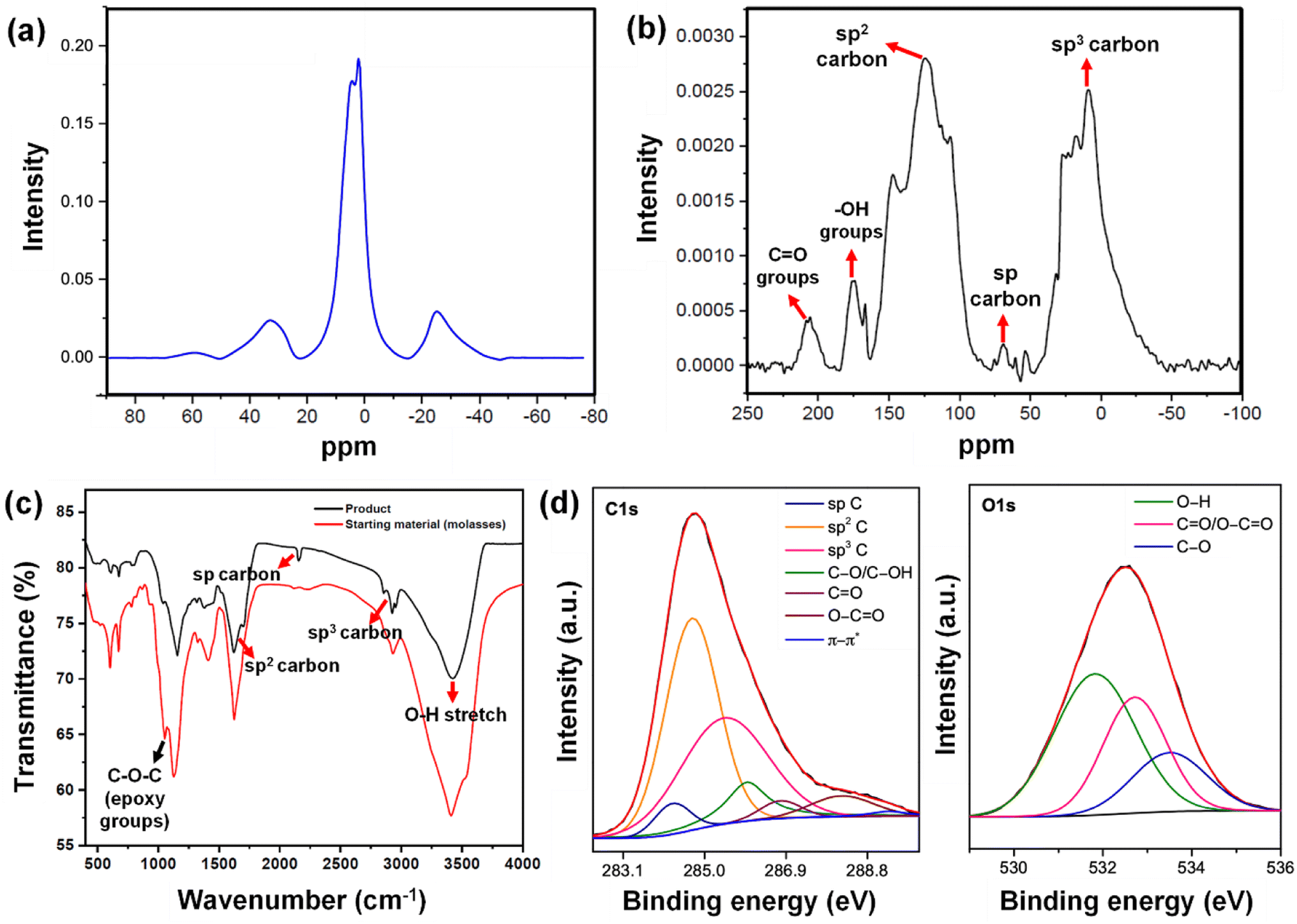
To elucidate a clear insight into the emergence of 1D carbyne nanocrystals from nano-constricted zones of 2D graphene nanolayers, a simple yet effective synthetic protocol for the formation of such intricate nanostructures has been studied by hydrothermal cutting of agro-industrial wastes (AW) and categorized into three major parts: crystal reorientation, hydrothermal cutting, and nanoconstriction formation. As reported in an earlier study,52 agro-industrial wastes are composed of a combination of major amorphous carbon phases with small crystalline domains. Hydrothermally treating AW resulted in a drastic decrease of cyclohexane monoclinic carbon phases, giving rise to largely graphene hexagonal phases and textured growth. The crystal reorientation from amorphous carbon phases towards graphene hexagonal phases is attributable to the dominating periodic arrangement of atoms under autogenous pressure and controlled temperature conditions.52 Here, Raman spectroscopy was employed to confirm the presence of graphene, depicting typical graphene features in most regions: the G band around 1580 cm−1, signifying the E2g phonon at the Brillouin zone (BZ) centre, and the D band around 1360 cm−1 due to the breathing modes of 6-atom rings (Fig. 1a).67,68 A broad hump at ∼2670 cm−1 characteristic of the 2D band is also evident in Fig. 1a. Intriguingly, the second-order Raman scattering process involving two intervalley inelastic scatterings with iTO phonon near the K point can be effectively interpreted to estimate the number of layers in graphene by scrutinizing the line shape and intensity.69 The broadened 2D band indicates the presence of multi-layer graphene.70 As a result, there are numerous possible double resonance scattering processes for 2D bands in multi-layer graphene. The 2D band located at ∼2670 cm−1 can be fitted by four Lorentzian peaks for AB stacked bilayer graphene71 (Fig. 1b (2D deconvoluted)). The wide band of the 2D peak in the Raman spectra can be attributed to the increase in defects and disorders caused by the formation of in-plane nanogaps on graphene layers72 (owing to hydrothermal-cutting of epoxy groups) during the autogenous pressurized hydrothermal-carbonization process.73 Interestingly, a band at ∼3300 cm−1 appears denoting the second order of D′ band termed as the 2D′ peak (Fig. 1c). Although this particular peak was less studied in the past, it originates from a Raman scattering process where momentum conservation is obtained by the participation of two phonons with opposite wave vectors to further confirm the presence of bilayer graphene.74 On further region-specific inspection of the sample using Raman spectroscopy, we found contrasting results, wherein both G and D bands possessed sizeable linewidths. This may be attributed to a conspicuous disorder in the latter case justified by the tendency of both G and D band linewidths to increase monotonously with disorder within the graphene matrix, although not in the same way since the G band could be affected by merging with the D′ band (Fig. 1d).75 The D′ band originates from a double resonance process; however, the double-resonance process is within the same Dirac cone unlike the D band for which the double resonance occurs in adjacent K and K′ Dirac cones in the Brillouin zone. Hence, it can be used to probe the nature of defects through the intensity criterion (Fig. 1e (G/D′ deconvoluted)).68,76 | ||
| Fig. 1 (a) Raman spectrum of Cp with a holey graphene-rich region. (b and c) Deconvoluted spectrum of the 2D and 2D′ band corresponding to (a). (d) Raman spectrum of Cp with a carbyne-rich region. (e) Deconvoluted spectrum of the G/D′ band along with (f) characteristic carbyne peak corresponding to (d). | ||
The presence of highly defective graphene in certain regions leads to non-hexagonal sp2 defects, which can be attributed to the occurrence of intrinsic defects that were formed to accommodate the edge states and strains.77 With narrowing nanoconstriction regions, energetically stable elongated carbyne chains may transpire from 2D graphene nanolayers. This accounts for the emergence of a stark carbyne peak while also retaining G and D bands indicative of disordered graphene. Bolstering the same, we observe a drop in I(D) in the Raman spectra (Fig. 1d), corresponding to an increase in the number of defects in graphene alongside a sharp decrease in I(2D), which can also be used as an indicator of disordered graphene.78 Remarkably, the emergence of a sharp Raman peak at ∼2100 cm−1 is observed around the disordered graphene regions generated by carbon triple bonds and offers strong evidence for the presence of carbyne crystals.29 The full-widths at half maximum (FWHM) value of this Raman peak becomes narrow, corresponding to the high purity and crystallinity of the carbyne nanocrystals that can be asserted to its significant presence in the sample. Notably, the characteristic carbyne peak (Fig. 1f) existing around 2145 cm−1 (FWHM = 7.966) affirms the presence of carbyne nanocrystals (peak width stretching around ∼30 cm−1 vibrations). These results were in good agreement with the photoluminescence spectra of the obtained Cp (Fig. S10†). The formation mechanism of carbyne nanochains from epoxy-rich graphene nanolayers were shown in Scheme 1.
 | ||
| Scheme 1 Schematic illustration of carbyne chain formation from the hydrothermal cutting of epoxy-rich graphene layers. | ||
3.2 Morphological characteristics of the nanomaterial
Corresponding to the contrasting compositional regions indicated by Raman spectroscopy, we performed high-resolution transmission electron microscopy (HRTEM) to recognize the basis of carbyne formation from graphene-rich AB bilayer sheets and its underlying mechanism. Consistent with the Raman findings, layered and highly porous holey graphene sheets guiding the origin of nanoconstricted lattices were observed in Fig. 2a (insets showing nanoconstrictions (1 and 2)). On further inspection of the graphene-rich areas, we found superimposed and close-packed sheets with maximized areal molecular density representing stacked moiré patterns (Fig. 2b–d). Few degrees of twist arising between the assembly of stacked layers of graphene nanosheets gives rise to moiré patterns, and such intricate domains show the existence of nanoconstrictions, which act as a preferential site for the formation of 1D carbyne nanochains.79 The magnified views of a selected region of Fig. 2a and FFT patterns corresponding to occurrences of unique lattice fringes are shown in Fig. 2b–d. HRTEM images at these edges of graphene demonstrate that there exist parallel fringes (Fig. 2b and c) and hexagonal patterns (Fig. 2d and e), which are possibly interrelated and originate through a similar mechanism: while the hexagonal patterns are from vdW interactions of graphene layers with rotational mismatches that are vertical to the microscope lens, the observation of parallel fringes comes from the projection of a similar superstructure but with a slight tilt in plane. A closer inspection of Fig. 2c also reveals variation in the widths of the stacking boundaries, indicating the probable occurrence of nanometre-wide transition areas between stacking domains. Moreover, we observe that these stacking boundaries typically consist of random alignments and exhibit a larger extent of regional contrast wherein few regions appear lighter than others, representing that the stacked boundaries can have distinct morphologies based on their specific synthesis conditions. Meanwhile, the light lines are absent in regions of graphene stacking. This selective induction of intensity decline at stacking regions can be described by the obstruction of electron beam diffraction during transmittance through bilayer graphene. Since HRTEM images are generated by electron scattering, the regional intensity is largely based on the diffraction peaks being utilized, consequent to a periodic lattice. In the case of bilayer graphene, as opposed to monolayer graphene, two layers assume a similar crystal orientation, leading to diffraction interference of layers with one another. Thus, the HRTEM intensity is influenced by phase differences or lattice periodicity shifts between the electron wave scattering by bilayer graphene.80,81 Intriguingly, the edges of these graphene layers depict a clear formation of (highlighted region in Fig. 2c) moiré patterns. The reduced image contrast at the stacking boundaries (dark lines in Fig. 2b–e), thus, indicates a phase difference in the transition areas (Δx1 is nonzero). We propose that this shift in phase can be explained by either relative shifting continuously between the layers due to strain on one of the layers or it can exist due to reconstructed graphene domains attributable to the formation of sharper stacking boundaries. Moreover, contrast variability in images insinuates a difference in the amounts of the shift in the lattice at the transitional areas, which may lead to different morphologies. | ||
| Fig. 2 (a) HRTEM images representing the orientation of layered holey graphene sheets (insets 1 and 2) depicting highly porous holey graphene regions with nanoconstricted lattice fringes, followed by (b–f) superimposed and close-packed sheets with maximized areal molecular density representing stacked graphene moiré patterns (with clear moiré images highlighted in (c)) and its corresponding FFT images ((b–e) scale bar: 5 nm−1). Further, the hierarchical nano-to-micro (g–k) structures are represented from scrolled layers of graphene (g) to the presence of intrinsic carbyne nanocrystals decoded from its characteristic hexagonal lattice packing system with the corresponding SAED pattern (l). | ||
3.3 Interfacial electronic properties of the material
Several topographical orientations of graphene moiré patterns with preferable defect densities were investigated using Scanning Tunneling Microscopy (STM) (Fig. 3a–f). To detect the magnetic fingerprints and electronic distribution states on graphene moiré patterns, differential conductance was observed at ambient conditions using STM, restricting their distribution closer to the Fermi energy (bias voltage of 20 mV). The STM measurements featuring dI/dV spectra probe the local density of electronic states (LDOS) along with the generation of periodic potential for graphene that can also be analysed for the determination of surface states of Dirac fermions. A sequence of STM measurements was conducted to analyse the interatomic distances at different parts of the observed moiré patterns since there is a variation in lattice extension for selective domain areas with respect to the other parts of the moiré pattern. A higher order of symmetry in the distribution of dI/dV curves can be attributed to the nearest-neighbour interlayer coupling induced by the hopping of electrons at the graphene sublattices breaking electron–hole symmetry. Generally, at the higher-energy regimes, the spectroscopy (dI/dV) tends to be smoothened, minimizing the graphene quasiparticle excitations, which eventually affects the identification of dips over dI/dV curves. Henceforth, we focused only on the low-energy regimes of graphene moiré patterns where the intervalley scattering gets neglected, showing the uniform distribution of dips along with apparent current density ranging from 0.01–0.03 nA, as shown in Fig. S1a–c.† The dI/dV curves were linear for most of the region (small dI/dV gradient), indicating a relatively small variation in LDOS that can be ascribed to the metallic nature in the closer proximity of defect centers. From the STM measurements, the origin of topological defects can be examined via typical meadows/cavities within the highly oriented protrusions (3D images) in a wide bias range (−400 mV to +400 mV), which strongly depends on the generated tunnelling current (i.e., from the tip–sample distance). The STM image in Fig. 3a–f shows a transition of crystalline ‘ripple’ domain boundaries to an extended regime of topological defects that can be attributed to the delocalized conduction electrons in graphene moiré edges and the presence of several magnetic impurities localized near the defect centers. The left corner of Fig. 3a, possessing a large protrusion in the form of a hillock, corresponds to the origin of defective sites leading to intricate vacancies majorly influenced by the lattice strain caused by out-of-plane carbon adatoms. Atomic force microscopy (AFM) also demonstrates the ‘ripple’ domains of graphene moiré edges (Fig. S1d†). The migration of carbon adatoms that are oriented in an out-of-plane symmetry from the graphene basal plane can affect the original planar structure to form a bridge configuration (on the top of the C–C bond in the basal plane).82 Subsequently, the change in the hybridization state at these lattice-constrained regimes can facilitate the intrusive formation of carbon linear chains due to nanoconstriction. The disappearance of periodicity at the edges of crystalline domains observed in Fig. 3a–f can be ascribed to the emergence of the nanoconstriction zone from the defective sites and at the edge states of the moiré pattern. Both the crest and trough regions of STM images (Fig. 3a–f) reveal the sublattice polarization by the arrangement of the uniform honeycomb structure of graphene. Some of the linear atomic orientation of carbyne nanochains with an interatomic distance of 0.31 nm was also observed (Fig. S8†). | ||
| Fig. 3 (a–f) Topographical orientations of graphene moiré patterns measured using scanning tunnelling microscopy. (g and h) Dielectric spectroscopic analysis of (g) the localization of electrons, (h) interfacial polarization effect, CV measurements of (i) Cp/SPCE at various concentrations of As3+ from 0.0001 μM to 100 μM with 5 mM K3Fe(CN)6/5 mM K4Fe(CN)6 as the electrolyte solution at a scan rate of 50 mV s−1, (j) EIS analysis of Cp representing the wide range of sensitivity depicting very high sensitivity even at the lowermost As3+ concentration. | ||
3.4 Electrochemical sensitivity and performance
Furthermore, the dielectric spectroscopic analysis suggests the accumulation of conduction electrons at the edge of the grain boundaries, improving the overall polarization as well as dielectric permittivity of the nanomaterial. Such predominant localization of electrons (Fig. 3g) and interfacial polarization effect (Fig. 3h) can offer greater potential for the fabrication of tailorable dielectric sensor devices. Later, we extended the scope of the sensor application by engaging the Cp for electrochemical-based As3+ sensing technique. By comparative current response, we observed that the bare SPCE current range was only ∼0.081 mA; however, using Cp-modified SPCE resulted in a much higher current profile of 0.091 mA. Subsequently, upon further addition of 100 μM As3+ solution, the current response carried a progressive jump to 0.096 mA (Fig. 3i). This phenomenon indicates that the carbyne-modified electrode demonstrated a significant increase in the peak current compared to the bare electrode. The proposed sensor showed a linear range from 0.0001 μM to 100 μM with an increased sensitivity of 0.22 mA μM−1. The Nyquist plot of the EIS spectra explains the electron transfer nature of the deposited film. The resistance created in the electrochemical system varies with an increase in the concentration of the analyte (arsenic solution) depending on the mobility of the electrons from the electrode to the electrolyte solution or vice versa. The results in Fig. 3j demonstrate that the Cp exhibits lower electron transfer resistance at lower concentrations (0.0001 μM) of the arsenic solution, which enhances the overall electron-transfer kinetics process correlating with higher sensitivity response.Furthermore, to investigate the real-time electrochemical sensing performance, Cp was modified with a Pt electrode (Pt–Cp) and examined by recording the linear sweep voltammetry (LSV) at diverse As3+ concentrations (Fig. 4a), detecting the As3+ presence in highly interfering electrolyte species (Na+, Hg2+, Cd2+ and Pb2+) using CV (Fig. 4b) and real-time sensing of As3+ in river water samples (Fig. 4c). LSV plots in Fig. 4a depicted the electrochemical sensing behaviour of various As3+ concentrations using the Pt–Cp electrode. Later, CV plots were examined under the same buffer solution composed of other interfering species (Na+, Hg2+, Cd2+ and Pb2+) along with As3+ species. Intriguingly, there was no pronounced decline in the As3+ peak intensity, indicating high selectivity and sensitivity of the electrocatalysts even in the presence of high concentrations of interfering species. A slight change in the peak intensity could be associated with resistance engendered by the larger ionic radii of divalent cations (Pb2+, Cd2+, Hg2+) in the buffer metal ions possessing larger ionic radii generating strong attraction towards the functionalities of Pt–Cp (Fig. 4b). To evaluate its environmental susceptibility in real time, we performed real-time measurements by collecting the groundwater samples at multiple source points along the banks of the Yamuna river (i.e. Hindon river traversing through Saharanpur, Muzaffarnagar, Meerut, and Baghpat districts in Uttar Pradesh India). The Hindon river sample was compared with the regular tap water sample. The river sample displayed a concentration of ca. 45 μg L−1 of As3+, while the regular tap water tested from the lab displayed no peak response for As3+. Subsequently, 100 μg L−1 of As3+ was added to the tap water and sensed for the presence of As3+via electrochemical studies (Fig. 4c). There was a very marginal amperometric drop with a relative standard deviation (RSD) of 2.7% while maintaining 97.3% of the initial peak current response. This indicates the high stability and reproducibility of the modified sensor for real-time As3+ determination.
 | ||
| Fig. 4 (a) LSV plots of Pt–Cp at different concentrations of As3+ (ranging from 5–200 μg L−1). (b) CV plots of Pt–Cp for As3+ detection in the presence of interfering species (Na+, Hg2+, Cd2+, and Pb2+). (c) Real-time sensing of Hindon river water for As3+ detection. | ||
3.5 Defect oriented magnetic response and polarization
The low frequency EPR (X-band (9.763 GHz)) technique has been utilized to investigate the origin of highly defective centres of graphene moiré patterns, which not only provides an insight into spin properties but also includes the presence of conduction electrons, unpaired spins, and dangling bonds generated due to the electronic states of different forms of carbon (Fig. S2†).83,84 Generally, the intensity of the D band in Raman data can be correlated with the presence of defect centers in the sample. In our experiment, the coupled D and G bands in the Raman spectra lie in accordance with the single broad EPR resonance shown in Fig. S2,† where the contribution of defects to the conductivity is consistent with unique crystallographic and electronic properties as shown in STM results (Fig. S1a–c†). To understand the intricate mechanism of the dependency of carbon-related defects on the microwave power, we determined the saturated behaviour of EPR spectra by qualitatively comparing the relaxation rates of paramagnetic centers keeping the frequency fixed at the resonance frequency of the resonator and sweeping the magnetic field over 200 G. However, only the EPR measurements taken at 2.965 mW indicate the in-phase steady saturation with an inhomogeneous broadening of the Gaussian line shape. Henceforth, the existence of such a single EPR signal can be attributed to the distinct zones of defects formed in the graphene moiré layers, particularly on the surface of graphene planes, edges, in-plane lattice defects along with oxygen-containing functional groups and no significant areas of planar sp2 carbon atoms.1,85Intriguingly, the sp3 hybridized defect centers are chemically active, causing strong charge carrier localization that may lead to the enhanced magnetism generated in graphene moiré patterns.86 Furthermore, the EPR spectrum and Raman bands follow the Kohn anomaly, which is evident from the broadening of D and G bands, indicating anharmonicity prevailing over the defect-related electron-phonon or phonon-mediated defect (inelastic scattering) interactions.87 This phenomenon can be correlated to the increase in the ID/IG ratio from 0.7976 to 0.9532 for the carbyne sample and also lies in accordance with the inelastic scattering of electrons corresponding to iTO phonons (A1g and E2g phonons) near the Brillouin center. The competing spin dynamic mechanisms can be understood via analysing the hyperfine splitting with anisotropic g-tensors possessing the value of 2.0068, which is quite higher than other related reports,88–90 indicating a sequence of a high degree of magnetic interactions from oxygen-centered radicals in association with carbon radicals.91 Additionally, the line widths in the EPR signal also confirm the major contribution of paramagnetic centers from the sp3 hybridized carbon network as affirmed by the measured value of resonance ranging less than 1 mT of the Gaussian line shape. This is also confirmed by the dramatic shifts in 1H NMR peaks indicating paramagnetism (Fig. 5a).92
 | ||
| Fig. 5 (a) 1H NMR spectrum of the Cp. (b) 13C NMR spectrum of the Cp. (c) FTIR spectra of the Cp and the starting material (molasses–AW). (d) Deconvoluted C 1s & O 1s XPS spectra of Cp. | ||
3.6 Spectroscopic analysis and MD simulation studies
In addition to the strain-induced lattice shifts and reassembled moiré patterns, we observed several nanogaps in the graphene sheets, giving rise to holey graphene. The 13C NMR analysis (Fig. 5b) shows a peak in the region of 124.2 ppm arising due to intact graphene regions. The chemical shift region between 75 and 65 ppm indicates the presence of acetylenic carbon –C![[triple bond, length as m-dash]](https://www.rsc.org/images/entities/char_e002.gif) C–. Furthermore, the NMR signal at around 69 ppm validates the presence of sp carbon, depicting the generation of the carbyne phase. The presence of a peak near 147.2 ppm indicates single vacancy defects in graphene, which reduces the shielding of these carbon nuclei.93 Consistent with the holey graphene, sp3 carbon peaks centering 9 ppm to 30 ppm are attributable to edge carbon atom chains in graphene generated by hydrothermal cutting. We also observed the retention of ketone groups and hydroxyl groups, which were indicated by the peaks at 205 ppm and 175 ppm, respectively. Bearing in mind the existence of reconstructed graphene domains, these nanogaps uphold the phenomenon of phase difference and strain between layers. The occurrence of the holey graphene layer calls for further mechanistic insights into its formation. The carbon–carbon triple bonds of carbyne (–CC– bonds) are commonly identified using Fourier transform infrared (FTIR) spectroscopy. The signal in the FTIR spectrum at ∼2150 cm−1 (Fig. 5c) was in good agreement with the previous reports, wherein a similar value for carbon–carbon triple bonds was observed (between 2000 and 2200 cm−1).94 This phenomenon is a clear identification of the asymmetric CC stretching IR vibration bands. Also, these results clearly depicted the presence of carbyne with one-dimensional sp hybridization, consisting of alternating single bonds and triple bonds. The spectra also indicated the presence of other bonds (e.g., epoxy at 1053 cm−1, alkoxy C–O at 1153 cm−1, and C
C–. Furthermore, the NMR signal at around 69 ppm validates the presence of sp carbon, depicting the generation of the carbyne phase. The presence of a peak near 147.2 ppm indicates single vacancy defects in graphene, which reduces the shielding of these carbon nuclei.93 Consistent with the holey graphene, sp3 carbon peaks centering 9 ppm to 30 ppm are attributable to edge carbon atom chains in graphene generated by hydrothermal cutting. We also observed the retention of ketone groups and hydroxyl groups, which were indicated by the peaks at 205 ppm and 175 ppm, respectively. Bearing in mind the existence of reconstructed graphene domains, these nanogaps uphold the phenomenon of phase difference and strain between layers. The occurrence of the holey graphene layer calls for further mechanistic insights into its formation. The carbon–carbon triple bonds of carbyne (–CC– bonds) are commonly identified using Fourier transform infrared (FTIR) spectroscopy. The signal in the FTIR spectrum at ∼2150 cm−1 (Fig. 5c) was in good agreement with the previous reports, wherein a similar value for carbon–carbon triple bonds was observed (between 2000 and 2200 cm−1).94 This phenomenon is a clear identification of the asymmetric CC stretching IR vibration bands. Also, these results clearly depicted the presence of carbyne with one-dimensional sp hybridization, consisting of alternating single bonds and triple bonds. The spectra also indicated the presence of other bonds (e.g., epoxy at 1053 cm−1, alkoxy C–O at 1153 cm−1, and C![[double bond, length as m-dash]](https://www.rsc.org/images/entities/char_e001.gif) O stretch at 1662 cm−1, etc.). The intensity of the OH band at ∼3414 cm−1 is reduced after the hydrothermal treatment, yielding a broad peak at ∼3428 cm−1. The FTIR peaks near ∼2925 cm−1 and ∼2956 cm−1 depicts sp3 C–H, corresponding to asymmetrical stretching and symmetrical stretching of methylene groups appearing post hydrothermal treatment. Plausibly, their formation is a consequence of hydrothermal cutting and validates the nanoconstriction phenomenon, finally forming a nanogap. The FTIR results were consistent with results from NMR and Raman spectroscopy. FTIR analyses (Fig. 5c) revealed the disappearance of the vibrational band of epoxy groups at 1054 cm−1 in the Cp obtained after the hydrothermal reaction. This can be attributed to the hydrothermal-assisted cleavage of epoxy edges in the precursor, which are fragile and susceptible to attack.95 The disappearance of the epoxy band suggests that they break up during the hydrothermal process, through which the bridging O atoms in the epoxy edges are removed. The resultant “unzipped” epoxy edges likely underwent expansion, leading to nanoconstricted areas by the merger of holes facilitated by hydrothermal cutting. The intensity of the OH band at 3414 cm−1 is reduced after the hydrothermal treatment, yielding a broad peak at 3428 cm−1. The peaks near 2925 cm−1 and 2956 cm−1, corresponding to asymmetrical stretching and symmetrical stretching of methylene groups appear post hydrothermal treatment. Plausibly, their formation is a consequence of hydrothermal cutting and validates the nanoconstriction phenomenon, finally forming a nanogap.
O stretch at 1662 cm−1, etc.). The intensity of the OH band at ∼3414 cm−1 is reduced after the hydrothermal treatment, yielding a broad peak at ∼3428 cm−1. The FTIR peaks near ∼2925 cm−1 and ∼2956 cm−1 depicts sp3 C–H, corresponding to asymmetrical stretching and symmetrical stretching of methylene groups appearing post hydrothermal treatment. Plausibly, their formation is a consequence of hydrothermal cutting and validates the nanoconstriction phenomenon, finally forming a nanogap. The FTIR results were consistent with results from NMR and Raman spectroscopy. FTIR analyses (Fig. 5c) revealed the disappearance of the vibrational band of epoxy groups at 1054 cm−1 in the Cp obtained after the hydrothermal reaction. This can be attributed to the hydrothermal-assisted cleavage of epoxy edges in the precursor, which are fragile and susceptible to attack.95 The disappearance of the epoxy band suggests that they break up during the hydrothermal process, through which the bridging O atoms in the epoxy edges are removed. The resultant “unzipped” epoxy edges likely underwent expansion, leading to nanoconstricted areas by the merger of holes facilitated by hydrothermal cutting. The intensity of the OH band at 3414 cm−1 is reduced after the hydrothermal treatment, yielding a broad peak at 3428 cm−1. The peaks near 2925 cm−1 and 2956 cm−1, corresponding to asymmetrical stretching and symmetrical stretching of methylene groups appear post hydrothermal treatment. Plausibly, their formation is a consequence of hydrothermal cutting and validates the nanoconstriction phenomenon, finally forming a nanogap.
HRTEM analysis revealed a highly crystalline cylindrical structure along with sheets of graphene in Fig. 2g–i. On closely inspecting the lattice structure, we observed a rectangular arrangement with a lattice spacing of 0.49 nm and (100) plane in one region, indicating crystalline carbyne (Fig. 2i).29 In other regions, rectangular and hexagonal lattice spacings of 0.165 nm, 0.31 nm, and 0.28 nm corresponding to planes (113), (203), and (210) confirmed the presence of carbyne (Fig. 2j).96 To further analyse the orientation of crystal planes and to interpret the concomitant emergence of carbyne crystals from periodically arranged graphene moiré patterns, XRD analysis was carried out. As shown in Fig. 6b, graphene exhibits a characteristic peak at 2θ = 25.58°, depicting the reflection planes (002) of the hexagonal phase of graphene (FWHM = 0.3967), which is correlated to an interlayer spacing of 3.47 Å. These dominating 2D hexagonal reflections were observed using the scattered peaks at 41.43°, 43.55°, and 55.86°, which indexed to (004), (101), and (222) planes, respectively (Fig. 6c). The higher angle (2θ) scattered peak at 55.86° with an in-plane lattice spacing of 0.164 nm confirms the stability of the graphene hexagonal phase over the other plausible phases. The narrow width of graphene peaks may be ascribed to two factors: (1) the large sheet size and (2) a relatively high domain order. However, the structural stability of the sp2 hybridized system is affected in due course of nanoconstriction experienced at the graphene hexagonal edges. Therefore, the emergence of the sp2–sp system is facilitated by nanoconstriction at the basal planes of graphene.
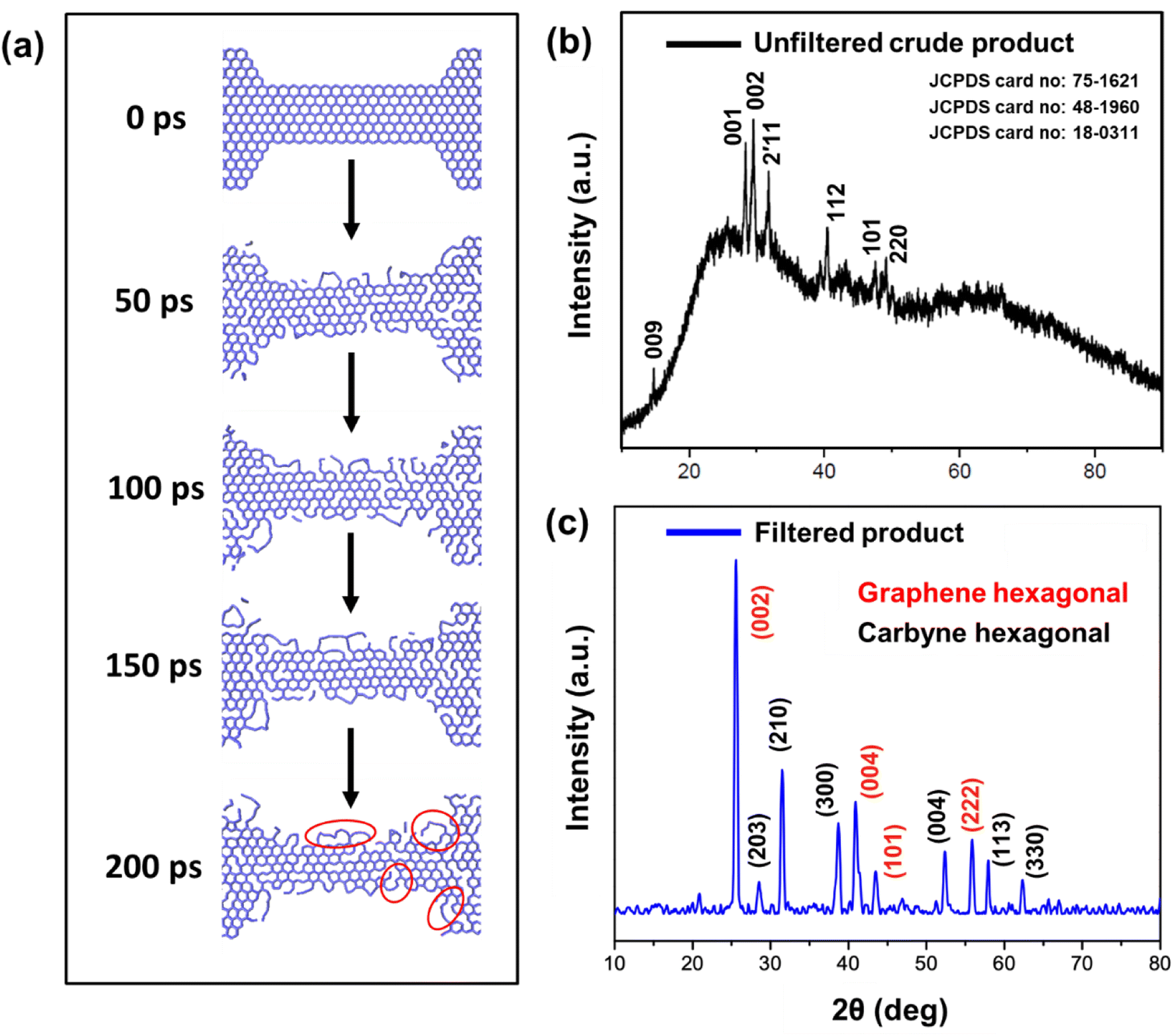 | ||
| Fig. 6 (a) Time course evolution study of the formation of carbyne nanochains from holey graphene strips calculated through MD simulation. The portions circled in red color show bent carbon chains (kinked) formed from graphene. (b) X-ray diffraction analysis for the unfiltered hydrothermal Cp, and (c) XRD patterns of the Cp (carbyne within graphene nanoconstriction) depicting the presence of graphene hexagonal (marked in red colour) and carbyne hexagonal phases (marked in black colour) after filtration treatment. | ||
X-ray photoelectron spectroscopy (XPS) and XRD analyses validate the formation of nanogaps in graphene owing to nanoconstriction. In the deconvoluted C 1s spectra (Fig. 5d), fitted with six peaks, the broadening effect of sp3 hybridized carbon at 285.4 eV indicates the local rehybridization of carbon atoms from sp2 to sp3 C atoms. This manifests highly reactive graphene defect sites such as edges, single vacancies, and grain boundaries.97 The broadening phenomenon of sp3 C atoms (FWHM = 2.39 eV) can be directly correlated to the increase in the concentration of defects,98 plausibly causing a zone of nano-constriction, and ultimately nanogaps (Fig. 2a).
The nanoconstriction-facilitated sp2–sp emergence, giving rise to carbyne nanocrystals is also indicated by XPS and XRD analyses. The low binding energy peak at 284.2 eV corresponds to the enhanced stability of sp hybridized carbyne nanochains nucleating from the dominating sp2 graphitic domains (284.7 eV), where the bridging of sp–sp2 clusters is the origin of molecular conductivity.99 The XRD pattern shows clean, shaped, strong peaks at 28.54°, 31.49°, 38.71°, 52.87°, 57.91°, and 62.33° depicted by the planes (203), (210), (300), (004), (113), and (330), respectively, which can be indexed to the hexagonal structure of carbyne (Fig. 6c and S7†). The predominance of highly crystalline carbyne peaks over graphene can be attributed to the existence of strong π electron delocalization of sp carbon atoms in comparison to the sp2 carbon atoms. Notably, the supremacy of sp2–sp hybridization is governed by the intricate Peierls distortion, resulting in the formation of finite carbyne nanochains and decreasing the degree of amorphization of crystalline carbyne domains.100 A minimum response of shake-up (0.9% of the total carbon content) of the valence electrons by the core hole expands the possible degeneracy of π sub-bands possessing minimum interband transitions within the confines of the Brillouin zone101 and the absence of inter-chain interactions, which is interpreted via higher in-plane lattice spacing of 0.148 nm (330) of α-carbyne as observed in XRD. The stability of carbyne nanochains relies concomitantly on the generation of periodic defects in graphene moiré patterns, causing periodic deformation/alteration on the bond lengths of sp-bonded C in the crystal lattices forming internal kinked structures similar to the effect of Peierls transition.101 The separation of carbyne chains from nanoconstricted graphene layers was modelled via simulation studies and represented using Visual Molecular Dynamics (Fig. 6a, S3 and S4) (ESI Video 1).† Similar to the methodology utilized in previous reports,60,102 we have also conducted a 200 ps NVT simulation using the Berendsen–Anderson temperature thermostat with a timestep of 0.2 fs. We also plotted the potential energy of the system with time and percentage of bonds broken to understand the trends in the reaction path (Fig. S3†).
4. Conclusion
In conclusion, we equipped a simple yet effective hydrothermal synthesis route using agro-industrial waste molasses to synthesize 1D carbyne nanocrystals within 2D graphene moiré nanolayers as a unique sp–sp2 hybridized system. The mechanism of carbyne nanocrystal formation in graphene moiré nanolayers accompanied by holey graphene packets occurs within a nanoconstricted zone, wherein we explored the hydrothermal cutting of epoxy-rich functional groups at graphene nanolayers. By deciphering the topographical properties of the nanomaterial using AFM and STM characterizations along with the dielectric measurements, the rich presence of hybridized defect sites, polarizability, and dielectric permittivity of holey graphene nanolayers with strong charge carrier localization were observed. Selected domains of electron diffraction in HRTEM analysis depicted a rectangular arrangement with a lattice spacing of 0.49 nm and (100) plane, indicating crystalline carbyne presence within graphene nanolayers. Furthermore, XRD patterns confirmed the presence of carbyne nanocrystals with characteristic peak (330) of the α-carbyne phase and dominating reflection planes (002) of the hexagonal phase of graphene (FWHM = 0.3967) with an interlayer spacing of 3.47 Å, ensuring the coexistence of carbyne nanocrystals and graphene moiré nanolayers. The separation of carbyne chains from nanoconstricted graphene layers was modelled via MD simulation studies to showcase a clear understanding of carbyne formation from graphene nanoconstriction. Excellent intrinsic properties of Cp, such as predominant localization of electrons, paramagnetic nature, dielectric permittivity, and real-time electrochemical sensitivity, especially in the case of As3+ sensing, explore a new arena in the development of sustainable next-generation electronic/sensor devices.Data availability
The raw/processed data required to reproduce these findings cannot be shared at this time as the data also forms part of an ongoing study.Author contributions
Sampathkumar Jeevanandham: methodology, investigation, visualization, data curation, validation, writing-original draft, writing-review & editing. Dakshi Kochhar: methodology, investigation, writing-original draft. Omnarayan Agrawal: investigation, data curation. Siddhartha Pahari: resources, visualization. Tamal Goswami: software, formal analysis. Chirantan Kar: methodology. Indra Sulania: investigation, validation. Monalisa Mukherjee: conceptualization, supervision, visualization, methodology, writing-original draft, writing-review & editing, project administration, funding acquisition.Conflicts of interest
All authors declare no conflicts of interest.Acknowledgements
Monalisa Mukherjee thanks the Department of Science and Technology (DST), Science and Engineering Research Board (SERB) (EMR/2016/005611) for funding and Amity University Uttar Pradesh (AUUP, Noida) for providing research infrastructure and library facility. We also acknowledge Ms Sujata Sangam for getting Raman spectra from JNU, New Delhi, and Inter-University Accelerator Centre (IUAC, Delhi) for providing instrumentation facilities.References
- A. K. Geim and K. S. Novoselov, Nat. Mater., 2007, 6, 183–191 CrossRef CAS PubMed.
- H. Ago, S. Okada, Y. Miyata, K. Matsuda, M. Koshino, K. Ueno and K. Nagashio, Sci. Technol. Adv. Mater., 2022, 23, 275–299 CrossRef PubMed.
- Y.-F. Huang, C.-Y. Chen, L.-C. Chen, K.-H. Chen and S. Chattopadhyay, NPG Asia Mater., 2014, 6, e123 CrossRef CAS.
- X.-C. Jiang, Y.-Y. Zhao and Y.-Z. Zhang, Phys. Rev. B, 2022, 105, 115106 CrossRef CAS.
- M. Yankowitz, J. Xue, D. Cormode, J. D. Sanchez-Yamagishi, K. Watanabe, T. Taniguchi, P. Jarillo-Herrero, P. Jacquod and B. J. LeRoy, Nat. Phys., 2012, 8, 382–386 Search PubMed.
- Y. Cao, V. Fatemi, S. Fang, K. Watanabe, T. Taniguchi, E. Kaxiras and P. Jarillo-Herrero, Nature, 2018, 556, 43–50 CrossRef CAS.
- A. K. Paul, A. Ghosh, S. Chakraborty, U. Roy, R. Dutta, K. Watanabe, T. Taniguchi, A. Panda, A. Agarwala, S. Mukerjee, S. Banerjee and A. Das, Nat. Phys., 2022, 1–8 Search PubMed.
- D. Deng, K. S. Novoselov, Q. Fu, N. Zheng, Z. Tian and X. Bao, Nat. Nanotechnol., 2016, 11, 218–230 CrossRef CAS PubMed.
- H. Jin, C. Guo, X. Liu, J. Liu, A. Vasileff, Y. Jiao, Y. Zheng and S.-Z. Qiao, Chem. Rev., 2018, 118, 6337–6408 CrossRef CAS.
- H. Yoo, R. Engelke, S. Carr, S. Fang, K. Zhang, P. Cazeaux, S. H. Sung, R. Hovden, A. W. Tsen, T. Taniguchi, K. Watanabe, G.-C. Yi, M. Kim, M. Luskin, E. B. Tadmor, E. Kaxiras and P. Kim, Nat. Mater., 2019, 18, 448–453 CrossRef CAS PubMed.
- A. K. Geim and I. V. Grigorieva, Nature, 2013, 499, 419–425 CrossRef CAS PubMed.
- J.-H. Zhong, J. Zhang, X. Jin, J.-Y. Liu, Q. Li, M.-H. Li, W. Cai, D.-Y. Wu, D. Zhan and B. Ren, J. Am. Chem. Soc., 2014, 136, 16609–16617 CrossRef CAS PubMed.
- L. Liao, H. Peng and Z. Liu, J. Am. Chem. Soc., 2014, 136, 12194–12200 CrossRef CAS PubMed.
- V. Meunier, A. G. S. Filho, E. B. Barros and M. S. Dresselhaus, Rev. Mod. Phys., 2016, 88, 025005 CrossRef.
- C. S. Casari, M. Tommasini, R. R. Tykwinski and A. Milani, Nanoscale, 2016, 8, 4414–4435 RSC.
- T. Do Minh, H. E. Gunning and O. P. Strausz, J. Am. Chem. Soc., 1967, 89, 6785–6787 CrossRef.
- O. P. Strausz, D. M. Thap and J. Font, J. Am. Chem. Soc., 1968, 90, 1930–1931 CrossRef CAS.
- O. P. Strausz, G. J. A. Kennepohl, F. X. Garneau, T. Do Minh, B. Kim, S. Valenty and P. S. Skell, J. Am. Chem. Soc., 1974, 96, 5723–5732 CrossRef CAS.
- F. Yang, C. Li, J. Li, P. Liu and G. Yang, ACS Nano, 2021, 15, 16769–16776 CrossRef CAS PubMed.
- A. Bino, M. Ardon and E. Shirman, Science, 2005, 308, 234–235 CrossRef CAS PubMed.
- B. Bogoslavsky, O. Levy, A. Kotlyar, M. Salem, F. Gelman and A. Bino, Angew. Chem., Int. Ed., 2012, 51, 90–94 CrossRef CAS PubMed.
- Q. Sun, L. Cai, S. Wang, R. Widmer, H. Ju, J. Zhu, L. Li, Y. He, P. Ruffieux, R. Fasel and W. Xu, J. Am. Chem. Soc., 2016, 138, 1106–1109 CrossRef CAS PubMed.
- L. Shi, R. Senga, K. Suenaga, H. Kataura, T. Saito, A. P. Paz, A. Rubio, P. Ayala and T. Pichler, Nano Lett., 2021, 21, 1096–1101 CrossRef CAS PubMed.
- C. S. Casari, A. Li Bassi, L. Ravagnan, F. Siviero, C. Lenardi, P. Piseri, G. Bongiorno, C. E. Bottani and P. Milani, Phys. Rev. B: Condens. Matter Mater. Phys., 2004, 69, 075422 CrossRef.
- W. A. Chalifoux and R. R. Tykwinski, Nat. Chem., 2010, 2, 967–971 CrossRef CAS PubMed.
- M. Brzhezinskaya and V. E. Zhivulin, Polym. Degrad. Stab., 2022, 203, 110054 CrossRef CAS.
- V. E. Zhivulin, L. A. Pesin, E. A. Belenkov, V. A. Greshnyakov, N. Zlobina and M. Brzhezinskaya, Polym. Degrad. Stab., 2020, 172, 109059 CrossRef CAS.
- M. M. Brzhezinskaya, V. M. Morilova, E. M. Baitinger, S. E. Evsyukov and L. A. Pesin, Polym. Degrad. Stab., 2014, 99, 176–179 CrossRef CAS.
- B. Pan, J. Xiao, J. Li, P. Liu, C. Wang and G. Yang, Sci. Adv., 2015, 1, e1500857 CrossRef PubMed.
- W. Cao, H. Xu, P. Liu, Y. He and G. Yang, Chem. Sci., 2023, 14, 338–344 RSC.
- Polyynes: Synthesis, Properties, and Applications, ed. F. Cataldo, CRC Press, Boca Raton, 2005 Search PubMed.
- H. E. Troiani, M. Miki-Yoshida, G. A. Camacho-Bragado, M. A. L. Marques, A. Rubio, J. A. Ascencio and M. Jose-Yacaman, Nano Lett., 2003, 3, 751–755 CrossRef CAS.
- C. Jin, H. Lan, L. Peng, K. Suenaga and S. Iijima, Phys. Rev. Lett., 2009, 102, 205501 CrossRef PubMed.
- A. Chuvilin, J. C. Meyer, G. Algara-Siller and U. Kaiser, New J. Phys., 2009, 11, 083019 CrossRef.
- G. Casillas, A. Mayoral, M. Liu, A. Ponce, V. I. Artyukhov, B. I. Yakobson and M. Jose-Yacaman, Carbon, 2014, 66, 436–441 CrossRef CAS PubMed.
- E. Kano, M. Takeguchi, J. Fujita and A. Hashimoto, Carbon, 2014, 80, 382–386 CrossRef CAS.
- M. T. Lusk and L. D. Carr, Phys. Rev. Lett., 2008, 100, 175503 CrossRef PubMed.
- S. Kutrovskaya, I. Chestnov, A. Osipov, V. Samyshkin, I. Sapegina, A. Kavokin and A. Kucherik, Sci. Rep., 2020, 10, 1–7 CrossRef PubMed.
- W. Cao, H. Xu, P. Liu, Y. He and G. Yang, Chem. Sci., 2023, 14, 338–344 RSC.
- Q. Sun, L. Cai, S. Wang, R. Widmer, H. Ju, J. Zhu, L. Li, Y. He, P. Ruffieux, R. Fasel and W. Xu, J. Am. Chem. Soc., 2016, 138, 1106–1109 CrossRef CAS PubMed.
- F. Yang, C. Li, J. Li, P. Liu and G. Yang, ACS Nano, 2021, 15, 16769–16776 CrossRef CAS PubMed.
- L. Shi, R. Senga, K. Suenaga, H. Kataura, T. Saito, A. P. Paz, A. Rubio, P. Ayala and T. Pichler, Nano Lett., 2021, 21, 1096–1101 CrossRef CAS PubMed.
- M. Brzhezinskaya and V. E. Zhivulin, Polym. Degrad. Stab., 2022, 203, 110054 CrossRef CAS.
- C. Jin, H. Lan, L. Peng, K. Suenaga and S. Iijima, Phys. Rev. Lett., 2009, 102, 205501 CrossRef.
- A. Chuvilin, J. C. Meyer, G. Algara-Siller and U. Kaiser, New J. Phys., 2009, 11, 83019 CrossRef.
- E. Kano, M. Takeguchi, J. Fujita and A. Hashimoto, Carbon, 2014, 80, 382–386 CrossRef CAS.
- K. Krishnamoorthy, V. K. Mariappan, P. Pazhamalai, S. Sahoo and S.-J. Kim, Nano Energy, 2019, 59, 453–463 CrossRef CAS.
- C. S. Casari, C. S. Giannuzzi and V. Russo, Carbon, 2016, 104, 190–195 CrossRef CAS.
- J. H. Scheidt, J. Nanomater., 2019, 2019, 1–8 CrossRef.
- R. Khanna, M. Ikram-Ul-Haq, A. Rawal, R. Rajarao, V. Sahajwalla, R. Cayumil and P. S. Mukherjee, Sci. Rep., 2017, 7, 16832 CrossRef PubMed.
- D. O'Hare, in Encyclopedia of Materials: Science and Technology, ed. K. H. J. Buschow, R. W. Cahn, M. C. Flemings, B. Ilschner, E. J. Kramer, S. Mahajan and P. Veyssière, Elsevier, Oxford, 2001, pp. 3989–3992 Search PubMed.
- S. Sangam, A. Gupta, A. Shakeel, R. Bhattacharya, A. K. Sharma, D. Suhag, S. Chakrabarti, S. K. Garg, S. Chattopadhyay, B. Basu, V. Kumar, S. K. Rajput, M. K. Dutta and M. Mukherjee, Green Chem., 2018, 20, 4245–4259 RSC.
- G. H. Major, N. Fairley, P. M. A. Sherwood, M. R. Linford, J. Terry, V. Fernandez and K. Artyushkova, J. Vac. Sci. Technol., A, 2020, 38, 061203 CrossRef CAS.
- M. Sobaszek, M. Brzhezinskaya, A. Olejnik, V. Mortet, M. Alam, M. Sawczak, M. Ficek, M. Gazda, Z. Weiss and R. Bogdanowicz, Small, 2023, 19, 2208265 CrossRef CAS PubMed.
- M. Brzhezinskaya, I. V. Mishakov, Y. I. Bauman, Y. V. Shubin, T. A. Maksimova, V. O. Stoyanovskii, E. Y. Gerasimov and A. A. Vedyagin, Appl. Surf. Sci., 2022, 590, 153055 CrossRef CAS.
- M. Brzhezinskaya, O. O. Kapitanova, O. V. Kononenko, S. Koveshnikov, V. Korepanov and D. Roshchupkin, J. Alloys Compd., 2020, 849, 156699 CrossRef CAS.
- A. C. T. van Duin, S. Dasgupta, F. Lorant and W. A. Goddard, J. Phys. Chem. A, 2001, 105, 9396–9409 CrossRef CAS.
- K. Chenoweth, A. C. T. van Duin and W. A. Goddard, J. Phys. Chem. A, 2008, 112, 1040–1053 CrossRef CAS.
- S. G. Srinivasan, A. C. T. van Duin and P. Ganesh, J. Phys. Chem. A, 2015, 119, 571–580 CrossRef CAS PubMed.
- S. G. Srinivasan and A. C. T. van Duin, J. Phys. Chem. A, 2011, 115, 13269–13280 CrossRef PubMed.
- W. Humphrey, A. Dalke and K. Schulten, J. Mol. Graph., 1996, 14, 33–38 CrossRef CAS PubMed.
- P. Giannozzi, S. Baroni, N. Bonini, M. Calandra, R. Car, C. Cavazzoni, D. Ceresoli, G. L. Chiarotti, M. Cococcioni, I. Dabo, A. D. Corso, S. de Gironcoli, S. Fabris, G. Fratesi, R. Gebauer, U. Gerstmann, C. Gougoussis, A. Kokalj, M. Lazzeri, L. Martin-Samos, N. Marzari, F. Mauri, R. Mazzarello, S. Paolini, A. Pasquarello, L. Paulatto, C. Sbraccia, S. Scandolo, G. Sclauzero, A. P. Seitsonen, A. Smogunov, P. Umari and R. M. Wentzcovitch, J. Phys.: Condens. Matter, 2009, 21, 395502 CrossRef PubMed.
- D. Vanderbilt, Phys. Rev. B: Condens. Matter Mater. Phys., 1990, 41, 7892–7895 CrossRef.
- H. J. Monkhorst and J. D. Pack, Phys. Rev. B: Solid State, 1976, 13, 5188–5192 CrossRef.
- S. Plimpton and J. Comput, Physics, 1995, 117, 1–19 CAS.
- Y. H. Hu, J. Phys. Chem. C, 2011, 115, 1843–1850 CrossRef CAS.
- F. Tuinstra and J. L. Koenig, J. Chem. Phys., 1970, 53, 1126–1130 CrossRef CAS.
- K. Krishnamoorthy, V. K. Mariappan, P. Pazhamalai, S. Sahoo and S.-J. Kim, Nano Energy, 2019, 59, 453–463 CrossRef CAS.
- L. M. Malard, M. A. Pimenta, G. Dresselhaus and M. S. Dresselhaus, Phys. Rep., 2009, 473, 51–87 CrossRef CAS.
- D. Graf, F. Molitor, K. Ensslin, C. Stampfer, A. Jungen, C. Hierold and L. Wirtz, Nano Lett., 2007, 7, 238–242 CrossRef CAS PubMed.
- C. S. Casari, C. S. Giannuzzi and V. Russo, Carbon, 2016, 104, 190–195 CrossRef CAS.
- Y. Bai, X. Yang, Y. He, J. Zhang, L. Kang, H. Xu, F. Shi, Z. Lei and Z.-H. Liu, Electrochim. Acta, 2016, 187, 543–551 CrossRef CAS.
- A. Milani, M. Tommasini, V. Russo, A. L. Bassi, A. Lucotti, F. Cataldo and C. S. Casari, Beilstein J. Nanotechnol., 2015, 6, 480–491 CrossRef PubMed.
- J. Zabel, R. R. Nair, A. Ott, T. Georgiou, A. K. Geim, K. S. Novoselov and C. Casiraghi, Nano Lett., 2012, 12, 617–621 CrossRef CAS.
- G. Pillet, A. Sapelkin, W. Bacsa, M. Monthioux and P. Puech, J. Raman Spectrosc., 2019, 50, 1861–1866 CrossRef CAS.
- A. Eckmann, A. Felten, A. Mishchenko, L. Britnell, R. Krupke, K. S. Novoselov and C. Casiraghi, Nano Lett., 2012, 12, 3925–3930 CrossRef CAS PubMed.
- J. K. Lee, G.-D. Lee, S. Lee, E. Yoon, H. L. Anderson, G. A. D. Briggs and J. H. Warner, ACS Nano, 2019, 13, 2379–2388 CAS.
- J.-B. Wu, M.-L. Lin, X. Cong, H.-N. Liu and P.-H. Tan, Chem. Soc. Rev., 2018, 47, 1822–1873 RSC.
- R. Bistritzer and A. H. MacDonald, Proc. Natl. Acad. Sci. U. S. A., 2011, 108, 12233–12237 CrossRef CAS PubMed.
- J. Lin, W. Fang, W. Zhou, A. R. Lupini, J. C. Idrobo, J. Kong, S. J. Pennycook and S. T. Pantelides, Nano Lett., 2013, 13, 3262–3268 CrossRef CAS PubMed.
- D. B. Williams and C. B. Carter, in Transmission Electron Microscopy: A Textbook for Materials Science, ed. D. B. Williams and C. B. Carter, Springer US, Boston, MA, 2009, pp. 23–38 Search PubMed.
- C. Cong, K. Li, X. X. Zhang and T. Yu, Sci. Rep., 2013, 3, 1195 CrossRef PubMed.
- A. Bateni, E. Erdem, S. Repp, S. Acar, I. Kokal, W. Häßler, S. Weber and M. Somer, J. Appl. Phys., 2015, 117, 153905 CrossRef.
- C. V. Pham, S. Repp, R. Thomann, M. Krueger, S. Weber and E. Erdem, Nanoscale, 2016, 8, 9682–9687 RSC.
- M. Kempiński, P. Florczak, S. Jurga, M. Śliwińska-Bartkowiak and W. Kempiński, Appl. Phys. Lett., 2017, 111, 084102 CrossRef.
- G. Z. Magda, X. Jin, I. Hagymási, P. Vancsó, Z. Osváth, P. Nemes-Incze, C. Hwang, L. P. Biró and L. Tapasztó, Nature, 2014, 514, 608–611 CrossRef CAS PubMed.
- S. Kasap, I. I. Kaya, S. Repp and E. Erdem, Nanoscale Adv., 2019, 1, 2586–2597 RSC.
- P. Stathi, D. Gournis, Y. Deligiannakis and P. Rudolf, Langmuir, 2015, 31, 10508–10516 CrossRef CAS PubMed.
- O. Marciano, S. Gonen, N. Levy, E. Teblum, R. Yemini, G. D. Nessim, S. Ruthstein and L. Elbaz, Langmuir, 2016, 32, 11672–11680 CrossRef CAS PubMed.
- C. V. Pham, M. Krueger, M. Eck, S. Weber and E. Erdem, Appl. Phys. Lett., 2014, 104, 132102 CrossRef.
- J. Kausteklis, P. Cevc, D. Arčon, L. Nasi, D. Pontiroli, M. Mazzani and M. Riccò, Phys. Rev. B: Condens. Matter Mater. Phys., 2011, 84, 125406 CrossRef.
- F. H. Köhler, in eMagRes, John Wiley & Sons, Ltd, 2011 Search PubMed.
- W. Qiu, Z. Chen and S. Zheng, Phys. E, 2020, 115, 113693 CrossRef CAS.
- Carbyne and Carbynoid Structures, ed. R. B. Heimann, S. E. Evsyukov and L. Kavan, Kluwer Academic, Dordrecht, Boston, 1999 Search PubMed.
- D. Pan, J. Zhang, Z. Li and M. Wu, Adv. Mater., 2010, 22, 734–738 CrossRef CAS PubMed.
- X.-Y. Chuan, Z. Zheng and J. Chen, Carbon, 2003, 41, 1877–1880 CrossRef CAS.
- Y.-C. Lin, C.-C. Lu, C.-H. Yeh, C. Jin, K. Suenaga and P.-W. Chiu, Nano Lett., 2012, 12, 414–419 CrossRef CAS.
- K. Ganesan, S. Ghosh, N. G. Krishna, S. Ilango, M. Kamruddin and A. K. Tyagi, Phys. Chem. Chem. Phys., 2016, 18, 22160–22167 RSC.
- A. Hu, S. Griesing, M. Rybachuk, Q.-B. Lu and W. W. Duley, J. Appl. Phys., 2007, 102, 074311 CrossRef.
- V. I. Artyukhov, M. Liu and B. I. Yakobson, Nano Lett., 2014, 14, 4224–4229 CrossRef CAS PubMed.
- Y. P. Kudryavtsev, E. M. Baytinger, F. F. Kugeev, Y. V. Korshak and S. E. Evsyukov, J. Electron Spectrosc. Relat. Phenom., 1990, 50, 295–307 CrossRef CAS.
- K. T. Nicholson, T. K. Minton and S. J. Sibener, J. Phys. Chem. B, 2005, 109, 8476–8480 CrossRef CAS PubMed.
Footnotes |
| † Electronic supplementary information (ESI) available. See DOI: https://doi.org/10.1039/d4na00076e |
| ‡ Equal contribution from authors. |
| This journal is © The Royal Society of Chemistry 2024 |