
 Open Access Article
 This Open Access Article is licensed under a Creative Commons Attribution-Non Commercial 3.0 Unported Licence
Multinary light absorbing semiconductor nanocrystals with diversified electronic and optical properties†
Soubantika
Palchoudhury
 *a,
Benjamin T.
Diroll
b,
Panchapakesan
Ganesh
c,
Jessica
Cobos
d,
Sohini
Sengupta
a and
Jingsong
Huang
*c
*a,
Benjamin T.
Diroll
b,
Panchapakesan
Ganesh
c,
Jessica
Cobos
d,
Sohini
Sengupta
a and
Jingsong
Huang
*c
aDepartment of Chemical and Materials Engineering, University of Dayton, Dayton, Ohio 45469, USA. E-mail: spalchoudhury1@udayton.edu; Tel: +1-937-229-3194
bCenter for Nanoscale Materials, Argonne National Laboratory, Lemont, Illinois 60439, USA
cCenter for Nanophase Materials Sciences, Oak Ridge National Laboratory, Oak Ridge, Tennessee 37831, USA. E-mail: huangj3@ornl.gov; Tel: +1-865-576-3991
dDepartment of Aerospace and Mechanical Engineering, University of Texas at El Paso, El Paso, Texas 79968, USA
First published on 4th June 2024
Abstract
We report multinary CuZn2ASxSe4−x semiconductor nanocrystals in a wurtzite phase, achieved via hot-injection synthesis. These nanocrystals exhibit a tunable bandgap and photoluminescence in the visible range. We employ density functional theory and virtual crystal approximation to reveal the bandgap trends influenced by the main group metals and S/Se alloying.
Introduction
There is an increasing demand for sustainable light absorbing as well as light emitting materials, crucial for next-generation clean energy devices and deep tissue bioimaging applications.1–3 Material choice in thin film solar cells, one of the most attractive solar energy conversion technologies, can greatly impact their performance. Although widely used as the absorber layer, Si is an indirect bandgap material with weak near-infrared (IR) absorption of the solar spectrum, which necessitates the thin film design of solar cells.4,5 In comparison, Cu-based chalcogenide semiconductor nanocrystals, which exhibit direct bandgap and absorption in the larger visible regime of the solar spectrum, have been explored to maximize the efficiency of thin film solar cells.6 Cu(In,Ga)Se2 (CIGS) thin film photovoltaics, for instance, have achieved an efficiency of ∼23%, the highest so far.7,8 There has been a continued search for materials composed of earth-abundant elements like Cu2ZnSnS4 (CZTS) to achieve desired grid parity, although at the cost of sacrificing the overall efficiency of the solar cell.9–12 To this end, multinary Cu-chalcogenide compositions have been explored as they offer a higher level of flexibility in terms of tunable bandgap and structure–property relation.13–16 Similarly, advanced materials play a pivotal role in biomedical imaging. Current research in this field focuses on deep tissue imaging and early-stage cancer detection,17,18 both of which require tunable light-emitting materials in the IR and visible regimes. However, most of the imaging agents currently used for deep tissue and early cancer diagnostics consist of toxic heavy metals like Hg, Cd, and Pb.19–21 Recently, Cu-based CuInSexS2−x/ZnS nanocrystals have shown great promise in bioimaging applications and are more biocompatible as compared to the heavy metal-based imaging agents.22,23 To this end, multinary Cu-chalcogenide semiconductor nanocrystals can offer a wider range of flexibility in emissive properties. However, these multinary semiconductor nanocrystal compositions are synthetically challenging to achieve.Herein, we report the colloidal synthesis of a new class of multinary CuZn2ASxSe4−x (A: Al, Ga, In; 0 < x< 4; CZASSe) chalcogenide semiconductor nanocrystals and a combined experimental and theoretical investigation of their composition-dependent optical and emissive properties. The composition, morphology, and crystal structure of the new semiconductor nanocrystals have been explored in detail via transmission electron microscopy (TEM), scanning electron microscopy energy dispersive X-ray (SEM-EDX), and X-ray diffraction (XRD), while the optical bandgap and emission properties of the corresponding chalcogenide compositions have been investigated via ultraviolet-visible spectroscopy (UV-vis) and photoluminescence (PL). Synergistic ab initio density functional theory (DFT) calculations employing both the Strongly Constrained and Appropriately Normed (SCAN) meta-Generalized Gradient Approximation (GGA) and Heyd–Scuseria–Ernzerhof (HSE06) hybrid functionals, in conjunction with the virtual crystal approximation (VCA), are used to elucidate the bandgap trends associated with the main group metals and S/Se alloying.24–26
Experimental and theoretical methods
We report in this section the synthesis and characterization of CuZn2ASxSe4−x (CZASSe, A: Al, Ga, In, 0 < x< 4) nanocrystals and the computational studies of the electronic properties using density functional theory.![[thin space (1/6-em)]](https://www.rsc.org/images/entities/char_2009.gif) 000 rpm, 30 min, Sorval™ Legend™ Micro 17 microcentrifuge, Fisher) for further characterization.
000 rpm, 30 min, Sorval™ Legend™ Micro 17 microcentrifuge, Fisher) for further characterization.
All the other compositions of CZASSe nanocrystals were synthesized using a similar process with stoichiometric quantities of the respective cationic and chalcogen precursors, keeping all other conditions the same. The reaction mixtures were heated to 300 °C for the CZAlSSe and CZGaSSe semiconductor nanocrystals.
Results and discussion
The novel CZASSe semiconductor nanocrystals have been synthesized via a modified hot-injection approach where the respective metal acetylacetonate salts serve as the multiple cationic precursors while a mixture of n-dodecanethiol (n-DDT)/tert-dodecanethiol (tert-DDT) and diphenyl diselenide serve as precursors for the multiple chalcogen anions. This is the first report of the synthesis of multinary Cu-chalcogenide nanocrystals of composition CuZn2ASxSe4−x containing both the S and Se chalcogens. Additionally, a comprehensive series of the CZASSe nanocrystals has been achieved in this study for the first time, where the substitution of S with Se has been varied from 0 to 100% (i.e., 0, 25, 50, 75, and 100%) and these five different S/Se substitutions have been realized for three different group III cations (i.e., Al, Ga, and In). It is not trivial to achieve multinary nanocrystals containing different cations and chalcogen anions within the same lattice. Therefore, the study provides a key achievement from the perspective of nanochemical synthesis. Fig. 1a shows the TEM image of a sample CZASSe composition, CuZn2InS2Se2 nanocrystals, which exhibit a plate-like morphology of ∼9 × 6 × 2 nm dimensions. The high crystallinity of the nanocrystal is evident from the regular lattice fringes in the high-resolution TEM (HRTEM) image (Fig. 1b). The lattice spacing of 0.24 nm correspond to (102) crystal plane of the wurtzite phase. The chemical composition of the nanocrystals based on the SEM-EDX analysis, Cu1.0Zn2.0In0.8S0.7Se1.1, is close to the stoichiometric composition in terms of the Cu:Zn:In and S:Se ratios, although it is deficient in anion composition (Fig. 1c). The deviations from stoichiometries suggest possible defects present on the surface of the nanocrystals. The core compositions for all synthesized nanocrystals can be identified to be stoichiometric CuZn2ASxSe4−x based on subsequent XRD measurements and DFT calculations.
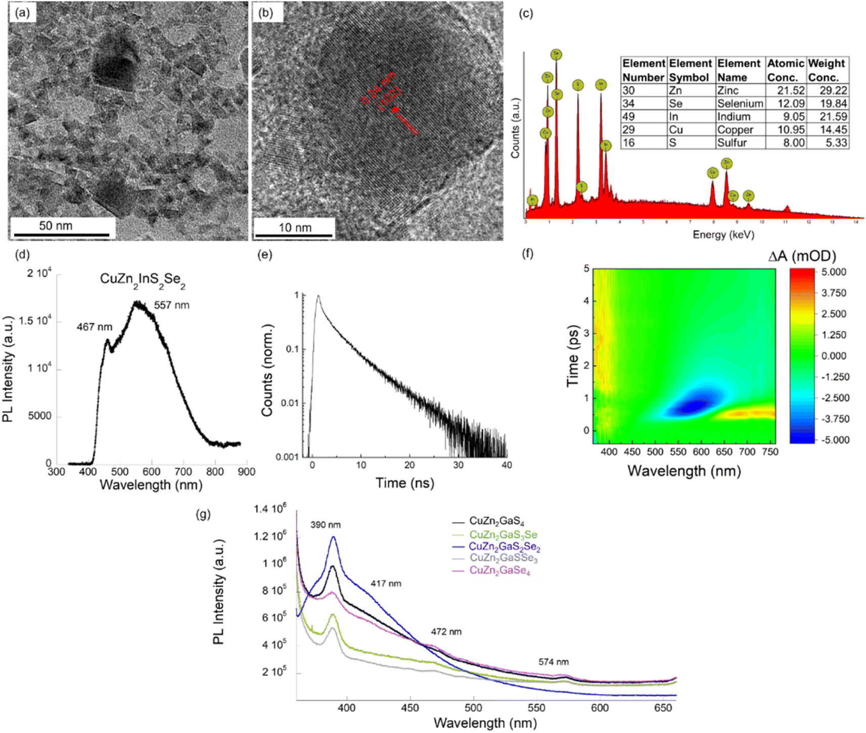 | ||
| Fig. 1 Characterization of CZASSe nanocrystals. (a) TEM image, (b) HRTEM image, (c) SEM-EDX characterization, (d) PL spectrum, (e) TRPL plot, (f) transient absorption, all for CuZn2InS2Se2 nanocrystals, and (g) PL spectra of various CuZn2GaSxSe4−x nanocrystal compositions. The results for other compositions are deposited in the ESI.† | ||
The CuZn2InS2Se2 nanocrystals also exhibit PL emissions in the blue (467 nm) and green (557 nm) visible ranges with an excitation at 350 nm (Fig. 1d). The emission in the blue region is attributed to organic materials such as the ligand, oleylamine and the S/Se sources. The representative time-resolved photoluminescence (TRPL) of the nanocrystals at room temperature, measured with a weak 405 nm pulsed laser source, 435 nm long-pass filter, and collected through a spectrometer is shown in Fig. 1e. The photoluminescence lifetime of the green emission is 4 ns. Transient absorption measurements (350 nm pump, visible probe) of the same sample show a bleach feature from 500–650 nm, which provides another measure of the direct band gap (Fig. 1f). The transient absorption signal decays rapidly, showing a substantial reduction in absorbance within a few ps, which is an indication of ultrafast charge trapping. The charge carriers are expected to be electrons, as revealed by subsequent electronic structure calculations. The SEM, EDX, and PL results for the other CZASSe compositions are shown in detail in the ESI (Fig. S1–S16†).
The composition-dependent change in the light-emitting properties of the CZASSe semiconductor nanocrystals has also been investigated. Fig. 1g shows the representative PL spectra of various compositions of the CuZn2GaSxSe4−x nanocrystals. Emissions in the violet region, i.e., peak at 390 nm with a broad shoulder at 417 nm, blue (472 nm), and yellow (574 nm) regions of the visible spectrum are observed for all CZGaSSe compositions without significant peak shifts. However, the PL intensities at 390 nm and 417 nm decreased progressively with increased Se substitution with the exceptions of CuZn2GaS2Se2 and CuZn2GaSe4. This can be attributed to the sizes of the respective nanocrystal compositions, i.e., the smaller size of 7.66 nm for CuZn2GaS2Se2 and the largest size of 13.17 nm for CuZn2GaSe4 (Table S1 and Fig. S17 ESI†). The PL intensity is the highest for the CuZn2GaS2Se2 composition that can be attributed to the reduced size of the nanocrystals. The peak height at 390 nm (violet regime) decreased consistently with Se substitution with the exceptions of CuZn2GaS2Se2 and CuZn2GaSe4, suggesting that the S chalcogen anion which decreased with Se substitution in the nanocrystal lattice may contribute to the emission at 390 nm.
The XRD structure of the CZASSe nanocrystals shows a pure wurtzite phase (space group: P63mc, no. 186).32 The XRD plots for two representative CZASSe compositions, CuZn2GaS3Se and CuZn2GaSe4, are shown in Fig. 2a and b, respectively. The major diffraction peaks at 2θ angles of 27.5°, 28.3°, 30.3°, 38.9°, 47°, 51.6°, 53.6°, 55.8°, and 59.4° for the CuZn2GaS3Se nanocrystals can be indexed to (100), (002), (101), (102), (110), (103), (200), (112), and (201) crystal planes of the pure wurtzite phase. The average particle size of the nanocrystals is estimated using the Debye–Scherrer formula, which relates the size of the nanocrystallites in a solid to the broadening of a peak in the diffraction pattern:33,34
 :Se atomic compositions of CuZn2AlSxSe4−x, CuZn2GaSxSe4−x, and CuZn2InSxSe4−x nanocrystals show a close match between the values calculated based on the experimental XRD of pure wurtzite phase, the DFT calculated crystal structures of CZASSe compositions, as well as the lattice parameters of CuZn2AS4 that we reported earlier (Fig. 2c).
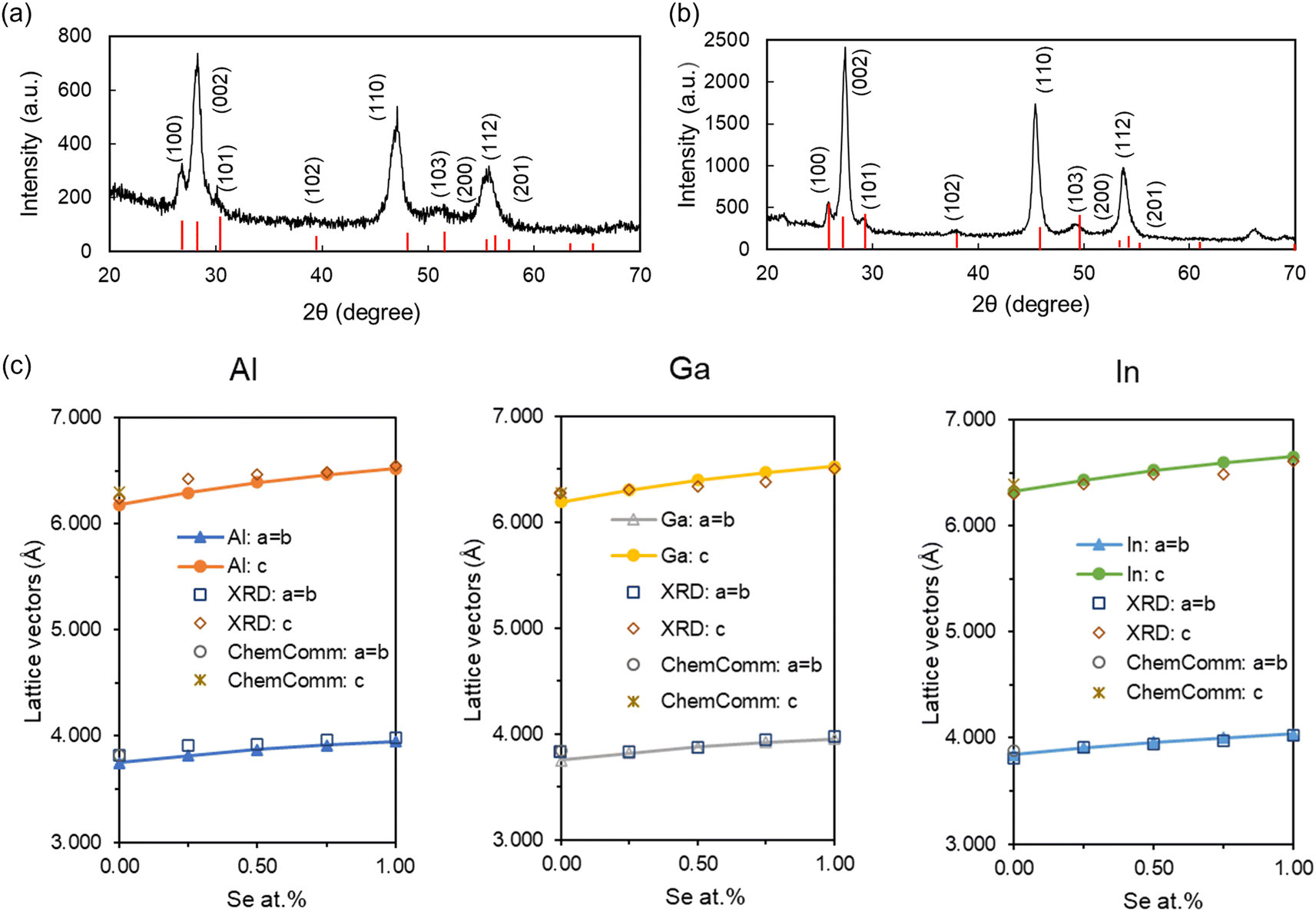 | ||
| Fig. 2 XRD characterization of pure wurtzite phase CZASSe semiconductor nanocrystals. (a) XRD plots of CuZn2GaS3Se nanocrystals and (b) XRD plot of CuZn2GaSe4 nanocrystals, where vertical lines represent peak positions obtained from theoretically relaxed crystal structures, and (c) plot showing a comparison of lattice parameters from theoretical three-dimensional structures, experimental XRD structures, and our previously reported CZAS nanocrystals in Chem. Commun.13 | ||
Both experimental and theoretical results indicate that the lattice parameters show an increasing trend with the progressive substitution of S atoms with the larger Se anion in the multinary chalcogenide compositions, as expected. The agreements of the diffraction peak positions and the lattice parameters validate the theoretically calculated crystal and atomic structures for all of the multinary chalcogenide compositions.
Using the theoretically relaxed geometries, we further calculated the electronic structures using both the SCAN meta-GGA and the HSE06 hybrid functionals for all of the multinary Cu-chalcogenide semiconductors synthesized in this work. Fig. 3a shows the unit cells of two representative CuZn2GaSxSe4−x compositions (i.e., CuZn2GaS4 and CuZn2GaSe4) that have been used for the electronic structure calculations. The unit cells of the other CZGaSSe compositions are shown in Fig. S22 (ESI†). Fig. 3b shows the band structure and density of state (DOS) calculated with HSE06 functional for two representative compositions of CuZn2GaSxSe4−x, one with S and other with Se. The electronic structures of the other S/Se and other CZASSe (A = Al and In) compositions are presented in the ESI (Fig. S23–S25†). All of these band structures display a direct bandgap at the Γ-point between valence and conduction bands with Dirac band characteristics.36 It is also worth noting that the conduction band is more dispersive than the valence bands; therefore, the mobility of electrons is expected to be higher than that of holes, making the former the dominant charge carriers, which are observed in the transient absorption signals (Fig. 1f). The bands with S and Se as the anions are similar but the bandgap is reduced upon replacement of S with Se. The bandgaps calculated by both SCAN meta-GGA and HSE06 hybrid functionals of the multinary CZASSe compositions decrease with increased size of the group III cation i.e., Al > Ga > In (Fig. 3c, d and S23–S25, ESI†). In addition, the bandgaps of the S/Se alloying compositions also show a clear trend of decrease with increased substitution of S with Se anions in the multinary unit cell until x = 0.75–1.00, where the bandgap becomes comparable (Fig. 3c and d). These trends align with observations in other materials where both chemical doping or mechanical stretching have been demonstrated to induce lattice expansions (as shown in Fig. 2c, 3c and d), consequently leading to reduced orbital overlaps and narrower spacings between bands.37 Between the results calculated with the two different functionals, the HSE06 bandgaps are significantly enhanced from the SCAN results. Nevertheless, they show the same trends with the compositional changes, in particular induced by the S/Se alloying, which significantly broadens and diversifies the electronic and optical absorption properties of CZASSe nanocrystals. It is worth pointing out that the HSE06 exchange–correlation functional, which is known for accuracy in bandgap predictions, produces bandgaps that fall in the visible range of ca. 1.5–3.2 eV, which are relevant for practical applications such as photovoltaics, photocatalysts, sensors, and light emitting diodes.
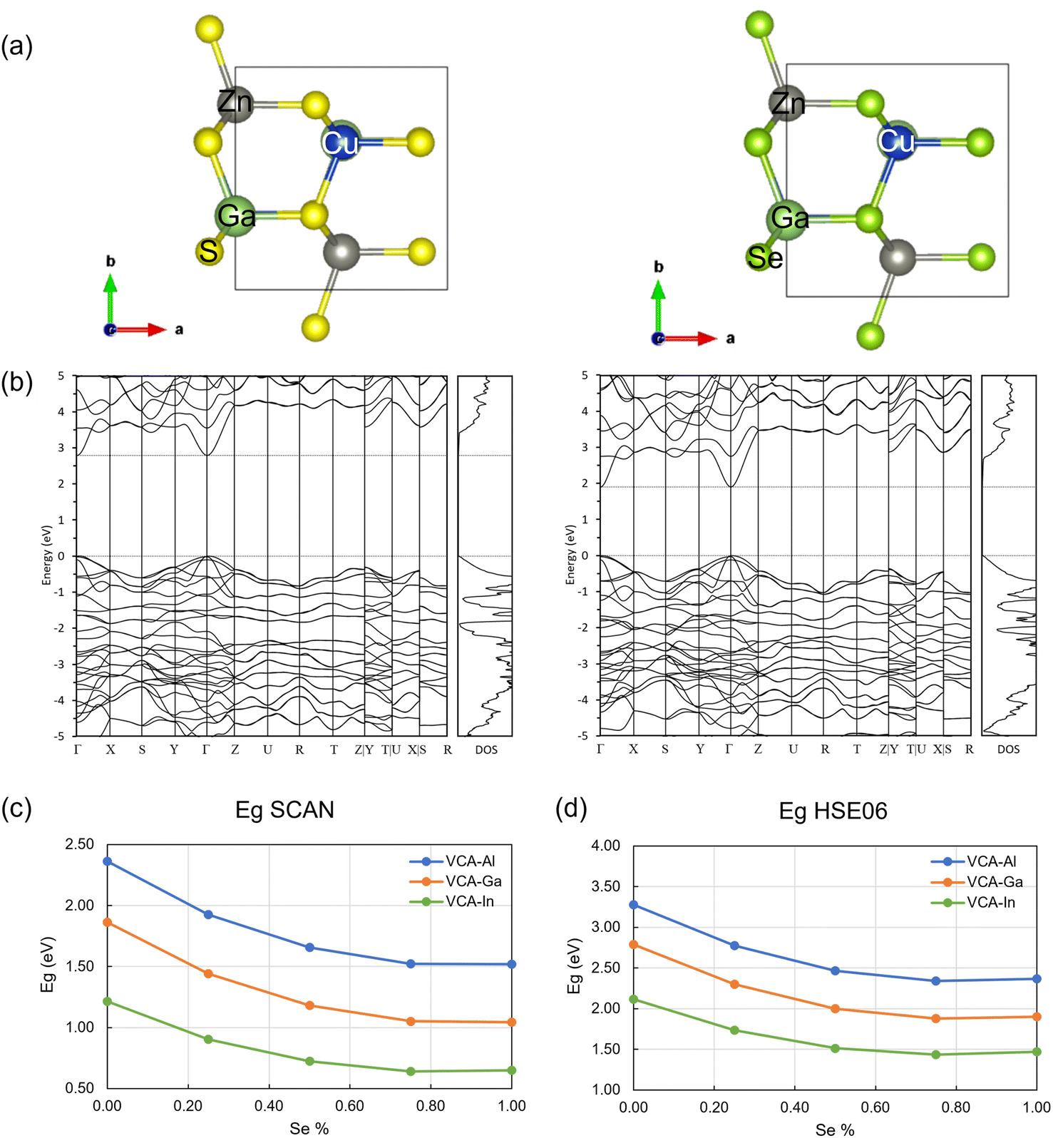 | ||
| Fig. 3 Theoretical bandgap predictions of CuZn2ASxSe4−x nanocrystals via SCAN and HSE06 hybrid functionals along with virtual crystal approximation. (a) Unit cells of wurtzite phase CuZn2GaS4 (left) and CuZn2GaSe4 (right) used for electronic structure calculations, (b) plots showing HSE06 band structures and density of states of CuZn2GaS4 (left) and CuZn2GaSe4 (right), respectively. (c) SCAN and (d) HSE06 calculated direct bandgaps of CZAlSSe, CZGaSSe, and CZInSSe as a function of atomic% of Se. | ||
The corresponding experimental optical properties of the CZASSe semiconductor nanocrystals are investigated via UV-vis spectroscopy of the well dispersed colloidal solutions of the nanocrystals in hexane. Fig. 4a shows the UV-vis spectrum of a representative CZASSe composition, CuZn2AlS2Se2 nanocrystals. The direct optical bandgap (Eg) of the semiconductor nanocrystals is determined by extrapolating the linear region of the Tauc i.e., (Aℏν)2versus ℏν plot, where A is the absorbance, ℏ is Planck's constant, and ν is the frequency of absorbed light. CuZn2AlS2Se2 nanocrystals exhibit a direct bandgap of 2.41 eV in the visible cyan regime of the visible solar spectrum, making it highly attractive for photovoltaic applications (Fig. 4b). Detailed experimental direct bandgap of each of the CZASSe nanocrystals is shown in the ESI (Fig. S26–S28†) and summarized in Table S1, ESI.† In general, the bandgap trend agrees with the theoretical ab initio predictions. However, the theoretical bandgaps have been calculated for bulk materials to reveal the general trends to be used as a reference, while experimental factors such as the size of nanocrystals, morphology, and defects can also play a role in the experimental bandgap of the semiconductor nanocrystals in addition to the S:Se composition.38–40 Therefore, the deviations from theory can be attributed to the variations of size, morphology, and defects in the CZASSe nanocrystals.
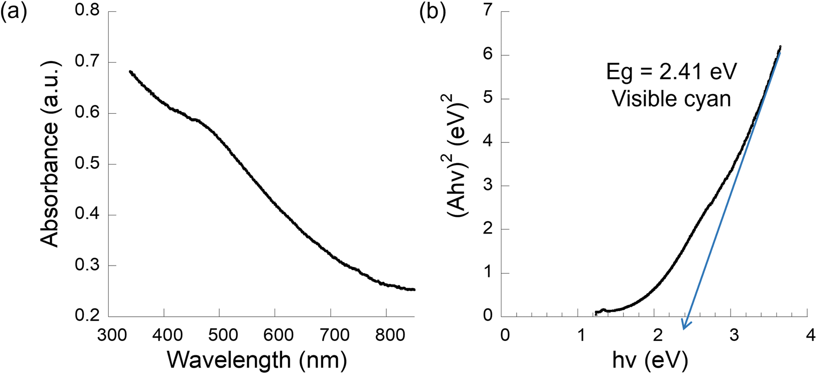 | ||
| Fig. 4 Experimental bandgap measurements of pure wurtzite phase CuZn2AlS2Se2 nanocrystals. (a) UV-vis plot and (b) Tauc plot showing direct bandgap. | ||
In this work, a novel class of multinary Cu-chalcogenide nanocrystals, CuZn2ASxSe4−x has been synthesized for the first time as new and more sustainable semiconductor materials with diversified electronic and optical properties for light absorbing and light-emitting applications. The new chalcogenide nanocrystals exhibit a wurtzite phase, as seen from the XRD structures and Rietveld refinement. The size and morphology of the nanocrystals have been characterized via TEM and SEM and show a highly crystalline wurtzite phase structure. The multinary semiconductor nanocrystals exhibit composition-dependent tunable direct bandgap and photoluminescence in the visible range, as suggested by the experimental UV-vis, Tauc, and PL plots. We also report the TRPL characterization of the new nanocrystals. Additionally, three-dimensional unit cells of the various multinary compositions have been modeled using DFT calculations employing the SCAN meta-GGA and HSE06 hybrid functionals, in conjunction with VCA approximation, which show close match with the experimental lattice parameters and diffractions from our XRD structures. A decrease in bandgap with increased size of the group III cation and increased substitution of S with the larger Se anion is predicted from the theoretical measurements. Size, morphology, and defect may also affect the physical properties of the multinary nanocrystals. For example, Fig. S17 (ESI†) shows the trend of experimental bandgap of the CZASSe nanocrystals. A comparison of the experimentally derived bandgap with that obtained using the two theoretical methods is shown in Table S1 (ESI†). In general, the HSE06 shows a closer match with experimentally derived bandgap. The calculations for CuZn2AS4 and CuZn2AS3Se compositions agree closely with experiment and larger deviations from experiment are observed with increased substitution of Se in the nanocrystal compositions. The deviation from experiment also increases with increased size of the group III cation in the CZASSe compositions (Table S1, ESI†). The experimental results display a general trend of decreasing bandgap with increasing amount of Se, which is confirmed by calculations. However, the effects of group III elements is not clear, which should be ascribed to other factors including particle sizes. In comparison, theoretical calculations also show the trend for group III elements. The bandgaps calculated with hybrid functional all fall in the visible range rendering them relevant for practical applications.
Author contributions
SP conceptualized the experiments, conducted the experiments, analyzed the results, and wrote the manuscript, SS conducted the syntheses and SEM characterization, JC contributed to the synthesis and manuscript revision, BD conducted the advanced TEM and PL analyses and wrote the manuscript, PG contributed to discussion and analysis of results and manuscript revision, and JH conceptualized the theory, conducted the theoretical calculations, analyzed the results, and wrote the manuscript.Conflicts of interest
There are no conflicts to declare.Acknowledgements
This work was supported by the Intel Ohio-southwest Alliance on Semiconductors and Integrated Scalable Manufacturing (OASIS) grant, and National Science Foundation REU Award #2244146, CNM ANL user project, and CNMS ORNL user project. TEM and TRPL were performed at the Center for Nanoscale Materials (CNM), a US Department of Energy Office of Science User Facility at Argonne National Laboratory, supported by the Office of Basic Energy Sciences under contract no. DE-AC02-06CH11357. DFT calculations were conducted at the Center for Nanophase Materials Sciences (CNMS), which is a US Department of Energy Office of Science User Facility at Oak Ridge National Laboratory.Notes and references
- L.-X. Yang, S. Zhang, B. Xu, J. Jiang, B. Cai, X. Lv, Y. Zou, Z. Fan, H. Yang and H. Zeng, Nano Lett., 2023, 23, 2443 CrossRef CAS PubMed.
- T. Todorov, O. Gunawan, S. Chey, T.-G. de Monsabert, A. Prabhakar and D.-B. Mitzi, Thin Solid Films, 2011, 519, 7378 CrossRef CAS.
- U. Ghorpade, M. Suryawanshi, S. Shin, K. Gurav, P. Patil, S. Pawar, C. Hong, J. Kim and S. Kolekar, Chem. Commun., 2014, 50, 11258 RSC.
- M.-A. Green, K. Emery, Y. Hishikawa, W. Warta and E.-D. Dunlop, Prog. Photovoltaics, 2016, 24, 3 Search PubMed.
- J. Zhou, X. Su, Q. Huang, B. Zhang, J. Yang, Y. Zhao and G. Hou, J. Mater. Chem. A, 2022, 10, 20147 RSC.
- S. Hadke, M.-L. Huang, C. Chen, Y. Tay, S. Chen, J. Tang and L. Wong, Chem. Rev., 2022, 122, 10170 CrossRef CAS PubMed.
- A. Kumar, A. K. Goyal, U. Gupta, Tanya, N. Gupta and R. Chaujar, Mater. Today: Proc., 2020, 28, 361 CAS.
- T.-S. Lopes, J.-P. Teixeira, M.-A. Curado, B.-R. Ferreira, A.-J.-N. Oliveira, J.-M. Cunha, M. Monteiro, A. Violas, J.-R.-S. Barbosa and P.-C. Sousa, et al. , npj Flexible Electron., 2023, 7, 4 CrossRef CAS.
- R.-B. Wexler, G.-S. Gautam and E.-A. Carter, J. Mater. Chem. A, 2021, 9, 9882 RSC.
- D.-B. Mitzi and Y. Kim, Faraday Discuss., 2022, 239, 9–37 RSC.
- J. Li, J. Huang, F. Ma, H. Sun, J. Cong, K. Privat, R.-F. Webster, S. Cheong, Y. Yao and R.-L. Chin, et al. , Nat. Energy, 2022, 7, 754 CrossRef CAS.
- W. Wang, M.-T. Winkler, O. Gunawan, T. Gokmen, T.-K. Todorov, Y. Zhu and D.-B. Mitzi, Adv. Energy Mater., 2014, 4, 1301465 CrossRef.
- A. Ghosh, S. Palchoudhury, T. Rajalingam, Z. Zhou, N. Naghibolashrafi, K. Ramasamy and A. Gupta, Chem. Commun., 2016, 52, 264 RSC.
- S. Palchoudhury, K. Ramasamy and A. Gupta, Nanoscale Adv., 2020, 2, 3069 RSC.
- S. Palchoudhury, K. Ramasamy, J. Han, P. Chen and A. Gupta, Nanoscale Adv., 2023, 5, 2724 RSC.
- F. Wang, Y. Han, C. Lim, Y. Lu, J. Wang, J. Xu, H. Chen, C. Zhang, M. Hong and X. Liu, Nature, 2010, 463, 1061 CrossRef CAS PubMed.
- Y. Li, Z. Li, X. Wang, F. Liu, Y. Cheng, B. Zhang and D.-L. Shi, Theranostics, 2012, 2, 769 CrossRef CAS PubMed.
- Quantum Leaps, Nat. Biotechnol., 2006, 24, 305 Search PubMed.
- A. Kamath, C. Melnychuk and P. Guyot-Sionnest, J. Am. Chem. Soc., 2021, 143, 19567 CrossRef CAS PubMed.
- S.-E. Keuleyan, P. Guyot-Sionnest, C. Delerue and G. Allan, ACS Nano, 2014, 8, 8676 CrossRef CAS PubMed.
- X. Liang, E.-G. Durmusoglu, M. Lunina, P.-L. Hernandez-Martinez, V. Valuckas, F. Yan, Y. Lekina, V.-K. Sharma, T. Yin and S.-T. Ha, et al. , ACS Nano, 2023, 17, 19981 CrossRef CAS PubMed.
- J.-Z. Kubicek-Sutherland, N.-S. Makarov, Z.-R. Stromberg, K.-D. Lenz, C. Castañeda, A.-N. Mercer, H. Mukundan, H. McDaniel and K. Ramasamy, ACS Appl. Bio Mater., 2020, 3, 8567 CrossRef CAS PubMed.
- Y.-T. Zhong, Z.-R. Ma, S.-J. Zhu, J.-Y. Yue, M.-X. Zhang, A.-L. Antaris, J. Yuan, R. Cui, H. Wan, Y. Zhou and W.-Z. Wang, et al. , Nat. Commun., 2017, 8, 737 CrossRef PubMed.
- J. Sun, A. Ruzsinszky and J.-P. Perdew, Phys. Rev. Lett., 2015, 115, 036402 CrossRef PubMed.
- J. Heyd, J.-E. Peralta, G.-E. Scuseria and R.-L. Martin, J. Chem. Phys., 2005, 123, 174101 CrossRef PubMed.
- L. Bellaiche and D. Vanderbilt, Phys. Rev. B: Condens. Matter Mater. Phys., 2000, 61, 7877 CrossRef CAS.
- G. Kresse, J. Non-Cryst. Solids, 1995, 193, 222 CrossRef.
- G. Kresse and J. Furthmuller, Phys. Rev. B: Condens. Matter Mater. Phys., 1996, 54, 11169 CrossRef CAS PubMed.
- P.-E. Blochl, Phys. Rev. B: Condens. Matter Mater. Phys., 1994, 50, 17953 CrossRef PubMed.
- G. Kresse and D. Joubert, Phys. Rev. B: Condens. Matter Mater. Phys., 1999, 59, 1758 CrossRef CAS.
- W. Setyawan and S. Curtarolo, Comput. Mater. Sci., 2010, 49, 299 CrossRef.
- X. Shen, E.-A. Hernandez-Pagan, W. Zhou, Y.-S. Puzyrev, J.-C. Idrobo, J.-E. Macdonald, S.-J. Pennycook and S.-T. Pantelides, Nat. Commun., 2014, 5, 5431 CrossRef CAS PubMed.
- A. O. Bokuniaeva and A. S. Vorokh, J. Phys.: Conf. Ser., 2019, 1410, 012057 CrossRef CAS.
- J.-M. Wu and Y.-R. Chen, J. Phys. Chem. C, 2011, 115, 2235 CrossRef CAS.
- T. Ratz, J.-Y. Raty, G. Brammertz, B. Vermang and N.-D. Nguyen, J. Phys.: Energy, 2021, 3, 035005 CAS.
- C. Hu, X. Zeng, Y. Liu, M. Zhou, H. Zhao, T. Tritt, J. He, J. Jakowski, P.-R.-C. Kent and J. Huang, et al. , Phys. Rev. B, 2017, 95, 165204 CrossRef.
- A. Chaves, J.-G. Azadani, H. Alsalman, D.-R. da Costa, R. Frisenda, A.-J. Chaves, S. Song, Y. Kim, D. He and J. Zhou, et al. , npj 2D Mater. Appl., 2020, 4, 29 CrossRef CAS.
- L. Brus, J. Phys. Chem., 1986, 90, 2555 CrossRef CAS.
- A.-M. Smith and S. Nie, Acc. Chem. Res., 2010, 43, 190 CrossRef CAS PubMed.
- T. Kippeny, L.-A. Swafford and S.-J. Rosenthal, J. Chem. Educ., 2002, 79, 1094 CrossRef CAS.
Footnote |
| † Electronic supplementary information (ESI) available: Experimental details for synthesis and characterization of the CZASSe nanocrystals, details of the computational studies, SEM and EDX analysis of the CZASSe nanocrystals, PL analysis of the CuZn2AlSSe and CuZn2InSSe nanocrystals, XRD analysis and Rietveld fit of the CZASSe nanocrystals, experimental bandgap and a table summarizing the bandgaps of CZASSe nanocrystals, and band structure and density of states of the CuZn2AlSSe and CuZn2InSSe nanocrystals. See DOI: https://doi.org/10.1039/d4na00043a |
| This journal is © The Royal Society of Chemistry 2024 |