DOI:
10.1039/D4NA00039K
(Review Article)
Nanoscale Adv., 2024,
6, 3251-3284
Frictional behavior of one-dimensional materials: an experimental perspective
Received
15th January 2024
, Accepted 8th May 2024
First published on 9th May 2024
Abstract
The frictional behavior of one-dimensional (1D) materials, including nanotubes, nanowires, and nanofibers, significantly influences the efficient fabrication, functionality, and reliability of innovative devices integrating 1D components. Such devices comprise piezoelectric and triboelectric nanogenerators, biosensing and implantable devices, along with biomimetic adhesives based on 1D arrays. This review compiles and critically assesses recent experimental techniques for exploring the frictional behavior of 1D materials. Specifically, it underscores various measurement methods and technologies employing atomic force microscopy, electron microscopy, and optical microscopy nanomanipulation. The emphasis is on their primary applications and challenges in measuring and characterizing the frictional behavior of 1D materials. Additionally, we discuss key accomplishments over the past two decades in comprehending the frictional behaviors of 1D materials, with a focus on factors such as materials combination, interface roughness, environmental humidity, and non-uniformity. Finally, we offer a brief perspective on ongoing challenges and future directions, encompassing the systematic investigation of the testing environment and conditions, as well as the modification of surface friction through surface alterations.
 Tursunay Yibibulla | Tursunay Yibibulla received her PhD degree in physics from Central South University in 2022. She currently works as a lecture at Nanning Normal University. Her primary research focuses on the synthesis and mechanical characterization of nanomaterials. |
 Lizhen Hou | Lizhen Hou received her PhD degree in School of Physics and Electronics from Hunan Normal University in 2008. She worked as a postdoctoral fellow at Central South University from 2012 to 2015 and at the University of Queensland in Australia from 2016 to 2018. She is currently a Professor at Hunan Normal University. Her research areas include the synthesis, manipulation, mechanical characterization, and applications of nanomaterials. |
 James L. Mead | James L. Mead received his PhD in 2019 from the University of Queensland (UQ), Australia, and was awarded the Dean's Award for Outstanding Research Thesis. He had also received his Bachelor of Mechanical Engineering & Material Science (Honours. Class I) from UQ. In 2020, he joined the Division for Microrobotics & Control Engineering at the University of Oldenburg, Germany, as a postgraduate researcher. His research interests include the mechanical characterisation of nanomaterials and nanoscale assembly, where he employs advance electron microscopy techniques. To date, he has authored more than 25 papers in international journals with a H-index of 11. |
 Han Huang | Huang Han received his PhD in 1995 from Western Australia University. He is serving as the Dean of the School of Advanced Manufacturing at Sun Yat-sen University and holding the esteemed position of Honorary Lifetime Professor at Queensland University, Australia. With a focus on areas like Nanomanufacturing, Additive Manufacturing, Ultra-Precision Machining, and Smart Manufacturing, he has contributed significantly, publishing nearly 300 academic papers in international journals. Notably, his invention of the Three-Dimensional Blade Automatic Grinding and Polishing System earned him the prestigious Singapore National Technology Award. |
 Sergej Fatikow | Sergej Fatikow received his PhD from Ufa Aviation Technical University (Russia) in 1988. In 1990, he initiated microrobotics research at University of Karlsruhe, Germany. He became a professor at University of Kassel in 2000 and established a new Division for Micro-robotics and Control Engineering (AMiR) at University of Oldenburg in 2001. As a full professor since 2001, his research spans microrobotics, industrial robotics, and nanohandling. Fatikow authored three books and over 150 papers and is the Founding Chair of the conference on Manipulation, Automation & Robotics at Small Scales (MARSS). |
 Shiliang Wang | Shiliang Wang received his PhD degree in Materials Science from Central South University (CSU) in 2008. He worked as an associate professor at CSU in 2009, and then he moved to the University of Queensland (UQ) in 2013 after being awarded the UQ Postdoctoral Research Fellowships. He is currently a Professor in the School of Physics at CSU. His research areas include nanomaterials, nanomechanics, nanomanipulation, biomimetic materials and technologies. To date, he has authored more than 120 academic papers in international journals. |
1. Introduction
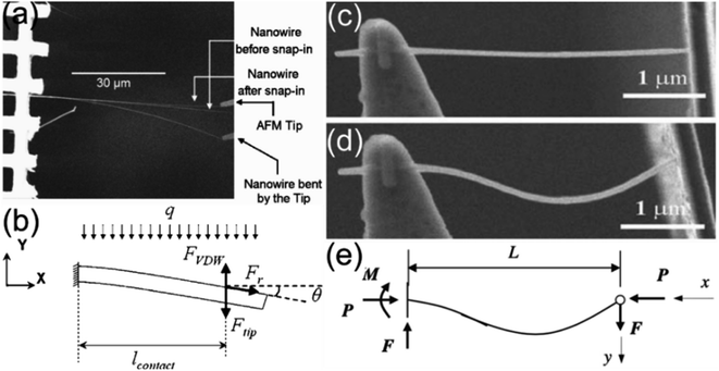
The outstanding mechanical,1–6 electrical,7–9 and optical10–13 properties of one-dimensional (1D) materials including nanofibers (NFs), nanowires (NWs), nanotubes (NTs), and nanorods (NRs), along with their high aspect ratio, large surface-to-volume ratio, and low defect density, have unlocked a plethora of exciting possibilities across various applications. These materials unlock tremendous potential across a wide array of applications, ranging from the micro/nanoelectromechanical systems (MEMS/NEMS) design14–17 to the development of nanogenerators for energy harvesting,18–25 and advanced material innovation26,27 to groundbreaking advancements in biomedical research.28–34 It is vital to underscore that the design, manufacturing, and utilization of these devices are intricately linked to a deep understanding of their surface frictional behavior, as it profoundly influences their performance across various domains.
Many nanogenerators, specifically piezoelectric and triboelectric nanogenerators (PENGs and TENGs), rely heavily on the intricate interplay between friction and energy harvesting efficiency.18–21,35–37 TENGs use electrostatic friction for charge transfer, where mechanical movement between different materials causes charge separation. Metal NWs, such as silver (Ag)38–42 and copper (Cu)43,44 showed best charge transfer efficiency, improving performance, as schematically shown in Fig. 1(a). A schematic diagram is presented to the operation of contact-mode TENG using a composite of polyvinylidene fluoride (PVDF)-Ag NW and nylon fibers. In PENGs, utilizing the piezoelectric effect, pressure or strain leads to mechanical deformation of piezoelectric materials, causing charge separation, so far semiconductor NWs, including zinc oxide (ZnO),45–47 silicon (Si),48,49 gallium nitride (GaN)50–52 and cadmium sulfide (CdS)53–55 have emerged as pivotal contributions in optimizing the energy conversion process. Their unique 1D structure renders them exceptionally well-suited for enhancing the efficiency of energy conversion. This is evident from the schematic setup for Fig. 1(b). However, practical applications pose a significant challenge for TENGs and PENGs due to unavoidable external mechanical contact on the triboelectric materials, leading to substantial wear and material adhesion. This results in nanogenerators being prone to wearing out by friction forces, causing a substantial decrease in durability that urgently needs to be addressed.56 To mitigate these friction-related issues, researchers are exploring some alternative 1D materials or new hybrid materials with high Young's modulus, hardness, and strength, or those possessing anti-wear properties and effective lubrication. For instance, such as carbon (C) NTs,57–61 which exhibit robust mechanical strength and low interlayer friction, effectively mitigating sliding friction between contacting surfaces. Mixing 0D62–69 and 2D materials with CNT leads to substantial reduction in friction across various surfaces,26,70–72 and thus have demonstrated the ability to effectively improve or partially alleviate the issues, as illustrated in Fig. 1(c). Therefore, the meticulous consideration of the frictional behavior exhibited by 1D materials becomes crucial in the optimization of nanogenerators. Understanding and harnessing the unique frictional properties of 1D materials play a pivotal role in fine-tuning TENGs for enhanced performance and efficiency in energy conversion processes.
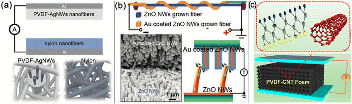 |
| | Fig. 1 Schematic diagram for nanogenerators based on 1D materials: (a) PVDF–Ag NW composite and nylon fibers based TENG. Reproduced with permission.41 Copyright 2017, Wiley. (b) ZnO NW based PENG. Reprinted with permission.73 Copyright 2008, Springer Nature. (c) Generating piezoelectric charges from a PVDF-CNT foam device. Reprinted with permission.61 Copyright 2019, Springer Nature. | |
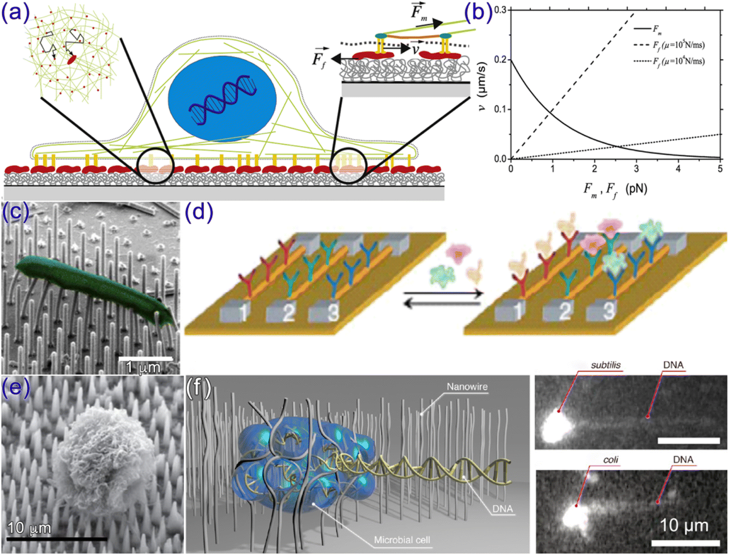
The role of friction in biomedical research is paramount when considering 1D materials. Specifically, the frictional forces between 1D materials and biological cells usually exert significantly influence over crucial cellular processes such as adhesion, spreading, and movement, as illustrated in Fig. 2(a)–(c).74–77 Meanwhile, the ability to control the frictional properties of 1D materials emerges as a guiding factor in shaping cell behavior, impacting fundamental cellular processes like differentiation, proliferation, and tissue regeneration.31,78,79 For example, in the tissue engineering and regenerative medicine, when designing scaffolds or substrates, the consideration of frictional properties becomes integral in replicating the native tissue environment. Optimized friction facilitates cell attachment, alignment, and tissue formation, thereby enhancing the success of tissue engineering approaches.80–82 Also, in drug delivery systems utilizing 1D materials as carriers for therapeutic molecules, the friction between these materials and the surrounding biological environment can crucially impact stability, release kinetics, and interactions with cells or tissues. A nuanced understanding and control of the friction of 1D materials could effectively contribute to enhancing the efficacy and specificity of drug delivery systems.83–85 Moreover, 1D materials have successfully found wide applications in the development of biointerfaces and biosensors, as shown in Fig. 2(d)–(f). In these applications, the frictional interaction between 1D materials and biological molecules or analytes directly influences their detection or sensing capabilities. Precision in controlling friction enhances the sensitivity, selectivity, and reliability of biosensing platforms, opening avenues for applications in diagnostics, monitoring, and biomarker detection of biosensing platforms, enabling applications in diagnostics, monitoring, and biomarker detection.86–88 Clearly, in-depth investigation, understanding, and controllable modulating of the friction behavior of 1D materials in biomedical research provide scientists and engineers with the opportunity to enhance their understanding of interactions with biological systems. This enables the development of innovative biomedical applications and advances the fields of tissue engineering, drug delivery, biosensing, and implantable devices.
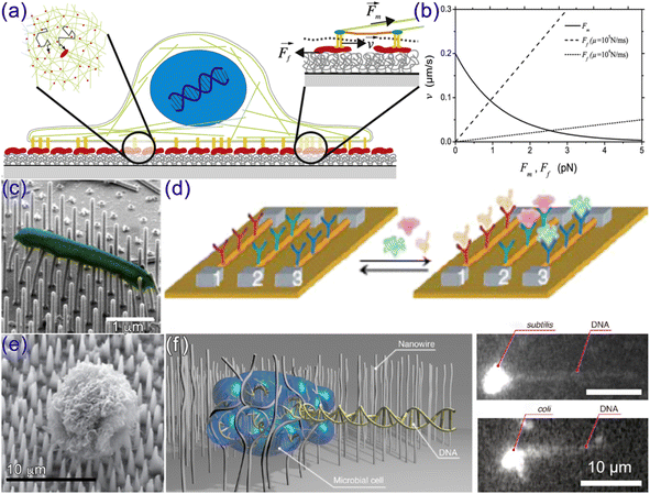 |
| | Fig. 2 (a and b) Frictional control model of traction forces of adherent cells by adhesion ligands on surfaces: (a) controlled movement of integrin–fibronectin complexes as they move directionally within the interlayer situated between the cell membrane and the substrate surface; (b) the relationship curve between velocity and the myosin motor characteristic force Fm (solid line) and sliding friction Ff (dashed lines) for ligand surface mobilities from 104 to 105 N ms−1. Reproduced with permission.74 Copyright 2011, Elsevier. (c) Scanning electron microscopy (SEM) image depicting the deformation of NWs upon direct contact with the attached cell body. Reproduced with permission.76 Copyright 2016, ACS. (d) Schematic of the multiplexed detection for cancer marker proteins using an Si NW array. Reproduced with permission.89 Copyright 2005, Springer Nature. (e) SEM image of NW interface with cell membrane. Reproduced with permission.84 Copyright 2015, ACS. (f) A schematic illustration of DNA extraction from microbial cells using NW in a microchannel. A fluorescence images of DNA extraction from a single cell of subtilis (Upper right) and coli (Bottom right). Reproduced with permission.34 Copyright 2019, ACS. | |
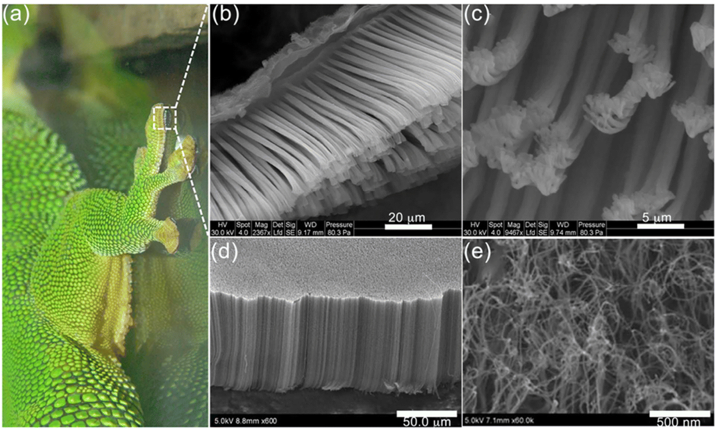
The exceptional adhesive capabilities demonstrated by geckos, as well as some spiders, beetles, and flies, has been ascribed to the compliance of the hierarchical fibrillar structures that exist on their toes or extremities. The compliance of these structures, which resemble a 1D array, is strongly influenced by the friction behavior associated with individual 1D fibrils as they contact adjacent fibrils or to the surface they are brought in contact with. The hierarchical structure of a gecko's foot consists of setae with thousands of nanoscale spatulae, as shown in the SEM micrographs in Fig. 3(a)–(c). These spatulae have specialized geometry and are also extremely compliant, permitting them to conform to a surface as it is brought into contact, maximizing the total area in contact, and therefore generating strong shear friction as well as strong adhesion force through van der Waals (vdW) interactions.90–97 Fundamental research into the frictional behavior of 1D materials has significantly improved our understanding of the high adhesion/friction strength, self-cleaning capability, and rapid attachment/detachment transition of hierarchical fibrillar structures. This understanding has also catalyzed the development of high-performance reversible dry adhesives. The development is exemplified by CNT-based adhesives that have demonstrated a tenfold increase in frictional force compared to a gecko's foot.47,92,98,99 A variety of optimized artificial adhesive systems that offer reversible adhesion have been demonstrating, facilitating reusability, repositionability, and damage-free removal.100–102
 |
| | Fig. 3 (a) Gecko foot attached to a glass substrate, (b) SEM images of setal array, and (c) spatulae at the tip. Reproduced with permission.103 Copyright 2004, Elsevier. (d) The vertically aligned CNT array and (e) the entangled top layer. Reproduced with permission.99 Copyright 2008, AAAS. | |
The fabrication and assembly of many of the devices and artificial adhesives outlined in this introduction requires the dedicated synthesis of 1D materials and customized integration strategies. Additional modification steps for the 1D material may also be required. A large quantity of literature that comprehensive reviews the application-specific synthesis, modification, and integration of 1D materials already exist, and therefore are considered to lay outside the scope of this review.98,104–112
To date, several reviews have been directly associated with the frictional characteristics of nanomaterials. For example, Schirmeisen et al. focused on the frictional behavior of nanoparticles on substrates using atomic force microscopy (AFM)-based manipulation techniques.113 Guo et al. discussed the advancements in friction research concerning low-dimensional materials, encompassing 1D and 2D materials.114 Additionally, Polyakov et al. focused on the friction of 1D materials on flat substrates under vacuum conditions, where real-time observation was provided by the SEM.115 These reviews collectively offer a valuable overview of experimental methodologies available for study the frictional behavior of 1D materials, and a deeper understanding of the underlying mechanisms. Nevertheless, the reviewed 1D friction studies are carried out on a limited variety of flat substrates and under specific test environment conditions. Furthermore, the most recently developed testing methodologies and the latest research findings on the frictional behavior of 1D materials have not yet been systematically compiled into a comprehensive review. Recognizing this deficit, this review has been composed to provide a thorough overview of experimental techniques developed over the past two decades for characterizing the frictional behavior of 1D materials. In the Second section, the review concisely clarifies the unique characteristics of 1D materials and also addressing the challenges in further developing our understanding. In the Third section, recent experimental strategies for measuring the frictional behavior of 1D nanomaterials are defined, their experimental results are summarized, and the associated experimental challenges are elucidated. In the Fourth section, a systematic analysis is provided on how the frictional behavior of 1D materials depends on various factors, including materials combinations, interface roughness, environmental humidity, and non-uniformity. Finally, the Last section discusses ongoing challenges and potential future directions in the field from our perspective.
2. Unique characteristics of the frictional behavior of 1D materials
Friction is the resistance force that arises at the interface when two contacting objects either undergo relative motion or exhibit a tendency for such motion. As researchers begin to investigate the friction behavior of nanoscale objects and between surfaces containing nanoscale features, the atomic spacing between the interacting surfaces diminishes to several Angstroms, and the discrete atomic structure inherent to each surface invariably influences the behavior of friction. As a result, friction behavior at the nanoscale can exhibit some unique characteristics or phenomena, for example, ultra-low friction nearing zero,116 negative friction coefficients,117,118 and the tendency for friction force to decrease with increasing normal load.118 The existence of such intricate phenomena has coined the term micro/nanofriction.119 The discovery of micro/nanofriction has brought into question our commonly held understanding of macroscale friction behavior. Consequently, to develop a full understanding of friction, it is imperative that researchers scrutinize the frictional dynamics of surfaces and interfacial molecular layers at the nanoscale by considering their molecular and atomic structures.
When discussing macroscopic friction and nanoscale friction, we are primarily addressing the manifestation of friction phenomena at different scales. Macroscopic friction, commonly observed in everyday life, is typically associated with the bulk properties of the volume of material within the interfacial region of interest, as depicted in Fig. 4(a). The fundamental assumption of macroscopic friction theories is that the objects or volumes of interest are continuous, dense entities that behave in a manner that can be described by continuum mechanics. Under such assumptions, the friction force is directly proportional to the applied normal load and can be described by Amonton's law:120–122F = µN, where F, µ and N are the friction force, friction coefficient, and external applied normal load, respectively. It is independent of the apparent contact area Aapparent. At the micro/nanoscale, however, friction is explained through single and multi-asperity models where the friction force primarily depends on the real or true contact area Atrue (defining the true contact area is nontrivial), and is suggested to express as F = σAxture, where σ is the interfacial shear strength, Atrue is the true contact area, and x is a exponent factor ranged from ranges from 0.25 to 1 depending on the commensurability of the surfaces.123,124
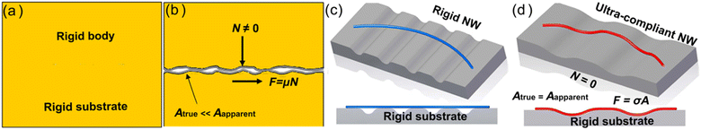 |
| | Fig. 4 Differences and similarities between macro and nanoscale friction: (a) macroscale contact and (b) microscale contact of rigid bodies. Reproduced with permission.125 Copyright 2009, IOP. (c) Rigid NW contact with rigid substrate and (d) ultra-compliant NW contact with rigid substrate. Here N is the applied normal force, Atrue is the true contact area, Aapparent is the apparent contact area, µ is the friction coefficient, and σ is the shear strength. Reproduced with permission.126 Copyright 2017, Springer Nature. | |
1D materials can exhibit unique friction characteristics due to their distinct structure; namely their high-aspect ratios and small diameters. Such unique friction characteristics can be observed when dragging or pulling a 1D material across a substrate. Depending on the mechanical compliance of the 1D material, it may either remain rigid or conform to the topography of the surface it is contact with, as shown in Fig. 4(c) and (d), respectively. The tendency of the 1D material to conform is dictated by the balance between the interfacial adhesion energy (the driving force for conformation) and the elastic energy associated with deflection of the 1D material (the resistance to conformation).127–131 The tendency of a 1D material to conform or not conform during sliding can lead to a non-constant friction force with respect to time, revealing distinctive frictional behavior.125,132,133 The ease at which a 1D material can conform can also give rise to novel “electro-capillary-elastic” coupling behavior, deviating from the conventional theory that frictional forces originate from electrostatic and capillary forces alone.134,135 In addition to the usual “static” friction and “kinetic” friction, there is also unique “rolling” friction, which has been found to significantly affect the frictional behavior of 1D material on a substrate.133,136–138 Numerous studies has shown that the structural geometry (primarily, length139 and diameter137,140) and conformability (either remaining rigid125,132,133 or conforming126) of a 1D material, as well as the anisotropic nature137,141 and time dependency142–144 of the interface motion can introduce further complexity in the frictional response. Nevertheless, the underlying mechanisms for such unique frictional behavior exhibited by 1D materials remain far from fully clarified.
Fundamentally, the single-asperity models have successfully explained frictional phenomena at the atomic-level, validated through an extensive range of AFM tests, theoretical calculations, and simulations over the past few decades.145–149 However, this idealized model is insufficient when applied to mesoscopic and macroscopic scales due to the increasing complexity of contact and friction behavior, leaving numerous questions unanswered. The unique geometric structures of 1D materials can result in distinct contact and friction behavior compared to traditional mesoscales. Therefore, investigating the frictional behavior of 1D material surfaces holds the potential to bridge the gap between the existing single-asperity models and real-world observations at mesoscopic and macroscopic scales. This, in turn, will not only guide the optimization of nanomaterial-based coatings,150–156 lubricants,157 and tribological systems,157 leading to improved performance and durability in various engineering applications, but will also benefit the design and development of nanoscale devices such as nanosensors,158–162 MEMS/NEMS,15,16,21,163 and nanorobots.164–167
3. Methods for characterizing the frictional behavior of 1D nanomaterials
Characterizing the frictional behavior of 1D materials necessitates addressing at least two specific technical challenges: (i) a means of inducing the 1D material to slip or exhibit the tendency to slip with respect to its contacting substrate surface, and (ii) a means of directly or indirectly measuring the lateral force responsible for inducing slip at the 1D interface. The first technical challenge is commonly accomplished through a contact-based nanomanipulation technique. In this approach, the slipping behavior of a targeted 1D material is induced by one or more nanoprobes, such as an etched W or Si cantilever tip. The position and movement of the tip as well as the induced movement of the 1D material itself can be visually monitored using a variety of microscopy techniques, AFM, SEM, transmission electron microscopy (TEM), or optical microscopy (OM). However, the second technical challenge generally demands sophisticated and intricate measurement devices and methods. In most cases, lateral forces in the range of µN to nN are measured directly, either by (1) an optical lever-based readout of an AFM cantilever, or (2) via dedicated force sensors which utilize piezoresistive, electrostatic, or capacitive mechanisms in combination with SEM, TEM, or OM. In recent years, a comparatively simpler indirect measurement strategy has been successfully developed, assessing frictional forces by directly observing the induced deformation of the targeted 1D materials using AFM, SEM, TEM, or OM.
3.1. AFM-based measurements
AFM can precisely generate the relative slip between 1D materials and substrates through the manipulation of a sensitive cantilever with a tip. The applied manipulation force can be determined from the cantilever deflection measured using a laser beam and a position-sensitive detector. The unique working principle of AFM makes it a powerful tool for studying the frictional behavior at nanoscale. Various AFM-based strategies have been developed to date for measuring the frictional behavior of 1D materials.
3.1.1. Direct measurement strategies.
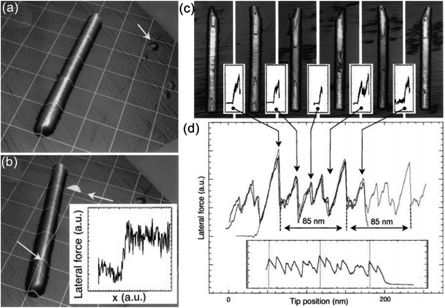
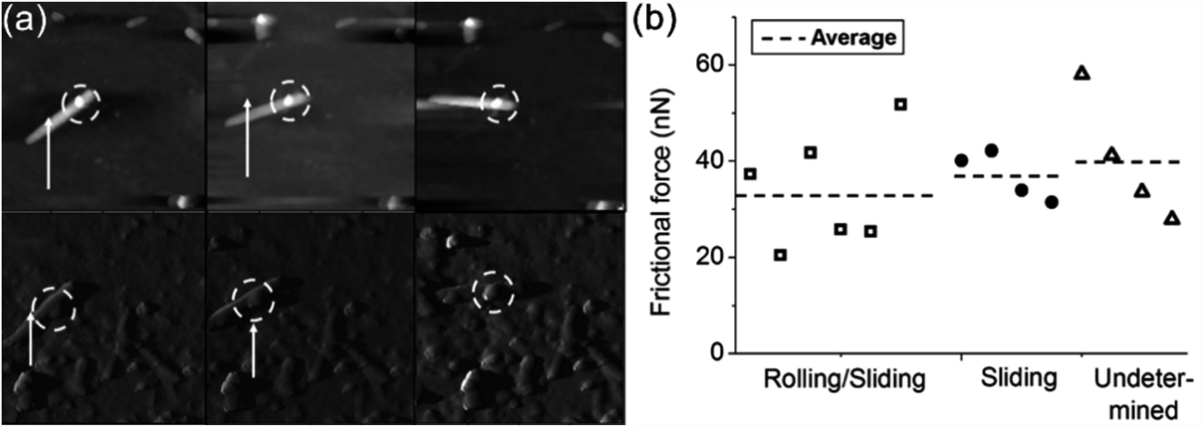
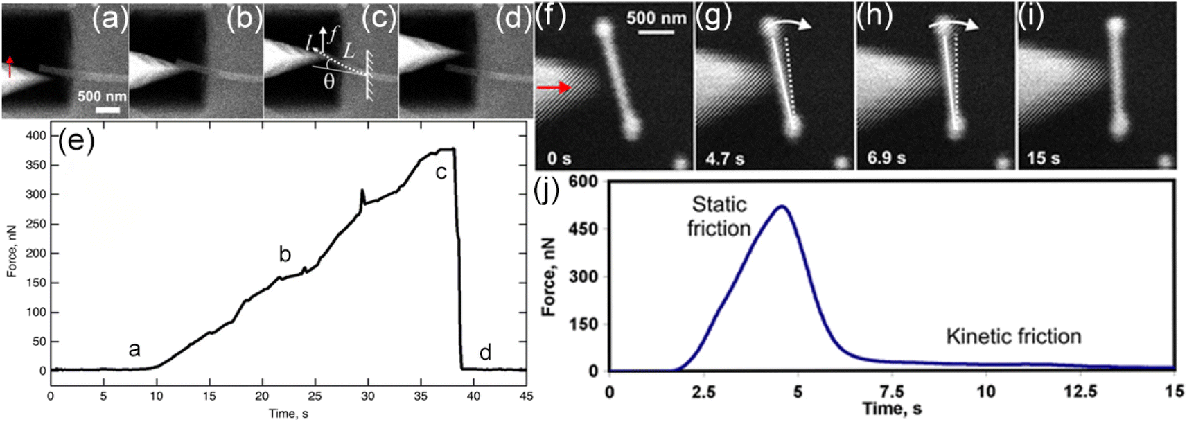
In 1999, Falvo et al. tested the frictional behavior of CNTs on mica and graphite substrates by the push forces collected from the AFM tip leading to the sliding or rolling of the CNTs (Fig. 5).136 In their study, a sliding friction force per unit length of 0.006 nN nm−1 and a sliding friction force per unit area of 2 MPa for a CNT with the average radius of 13.5 nm was obtained. Moreover, distinct behaviors were identified for a CNT sliding on mica and graphite substrates by end and side, respectively. On mica, when the CNT slid from its end, end-on pushes resulted in a noticeable initial stick–slip peak in the lateral force trace, as depicted in Fig. 5(b). In contrast, side pushes on mica produced a smooth lateral force trace accompanied by an in-plane rotation of the NT, and no initial stick–slip peak was observed, as depicted in Fig. 5(b). However, on graphite, during the side-on pushes, they not only observed the smooth lateral force trace with in-plane rotation (indicating sliding) but also instances where the CNT displayed a pronounced periodic stick–slip modulation, which they termed rolling, as shown in Fig. 5(c) and (d). Subsequently, Kim et al. further investigated the rolling and sliding behavior of short ZnO NWs on Si substrate by the manipulation technique using a Si AFM tip. Both sliding and rolling behaviors of the NWs were detected using the lateral mode of AFM, as depicted in Fig. 6(a) and (b). Furthermore, they also identified a coexistence of rolling and sliding during the manipulation, with some areas exhibiting indistinguishable characteristics. Their analysis yielded unprecedented high friction coefficients of 242 and 462.138
 |
| | Fig. 5 (a and b) AFM images of CNT's original position and after sliding. Inset in (b) shows the lateral force profile during the sliding manipulation. (c and d) AFM images of the during rolling and corresponding lateral force profile of a CNT. Reproduced with permission.136 Copyright 1999, Springer Nature. | |
 |
| | Fig. 6 (a) AFM images of the translation motion of ZnO NW during manipulation when both pure sliding and rolling sliding. The arrow indicates the motion of the probe tip, while the dotted circle indicates the marker on the NW used to assess the degree of rolling. (b) Average dynamic frictional forces measured during the manipulation. Reproduced with permission.138 Copyright 2013, RSC. | |
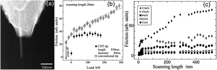
In 2002, Ishikawa et al. affixed a MWCNT onto the tip apex of a commercial silicon nitride (SiN) cantilever, as depicted in Fig. 7(a) and subsequently tested the friction behavior between the CNT and mica substrate by sliding the CNT on the mica surface. Despite the challenges in directly measuring the absolute values of frictional forces, they chose to gauge the output voltage proportional to the frictional force. Fig. 7(b) and (c) shows the dependences of frictional force on the external load and scanning length. It was found that the CNT tip exhibited a completely different behavior from that of conventional tip, attributed to the unique shape of CNT. Furthermore, a notable scanning length dependency of the friction force is observed due to the deformation of CNT.168
 |
| | Fig. 7 (a) MWCNT attached to AFM tip. (b) Friction versus load curves for both conventional and CNT probes were generated through the analysis of a scanning length set at 20 nm. (c) Friction and scanning length relationship diagram at various applied loads. Reproduced with permission.168 Copyright 2002, Elsevier. | |
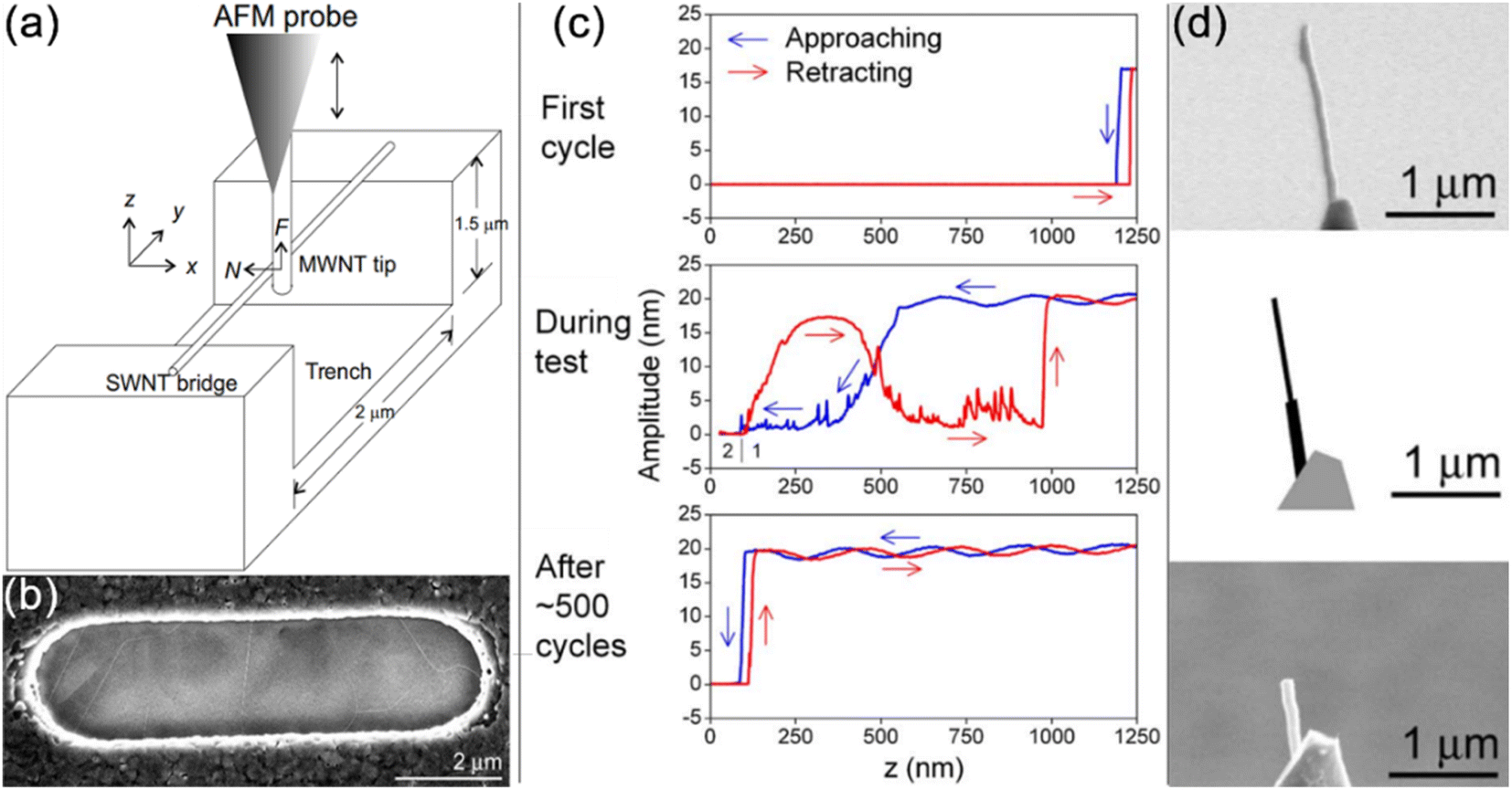
In 2008, Bhushan et al. developed a new method for measuring the friction between two individual CNTs, by sliding a CNT welded onto the Si AFM tip over another CNT suspended over a microtrench, as schematically shown in Fig. 8(a). They used the MWCNT-tipped probe to continually scanned horizontally169 and vertically170 over the SWCNT in a crossed geometry, as depicted in Fig. 8(a) and (b). In their first horizontal scanning experiments, they employed tapping mode of the AFM, calculated the experimental value of friction coefficient 0.006 ± 0.003 resulting from the interaction between the two CNTs, which caused changes in tapping amplitude. The tapping amplitudes and corresponding SEM images of the CNT tip during different cycles of scanning are illustrated in Fig. 8(c) and (d). Additionally kinetic shear strength 4 ± 1 MPa by using continuum mechanic model.169 And found remarkably unexpected results with a friction coefficient of 0.2 and a kinetic shear strength of 1.4 GPa during their vertical scanning experiments conducted in force-calibrated mode.170 Their experiments mark the pioneering endeavors in the historical pursuit of determining the frictional properties of individual 1D materials. But the substantial difference between the results of the two experiments may be attributed to the lack of visualization in the AFM operating process or the isotropic feature of the CNTs.
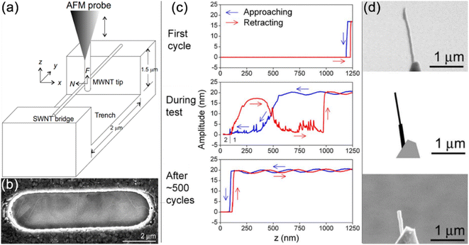 |
| | Fig. 8 (a) Experimental schema for testing the frictional behavior between two individual CNTs. (b) SEM image of CNTs suspended on the top of a microtrench made of polycrystalline Si. (c) Cantilever tapping amplitude and (d) SEM profiles of the MWCNT tip during the first cycle, during the test, and after ∼500 cycles. Reproduced with permission.169 Copyright 2008, APS. | |
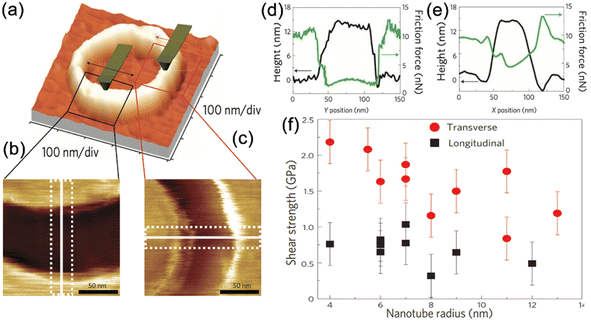
In 2009, Lucas et al. further investigated the rolling and sliding friction behavior of Si-supported CNTs by scanning the MWCNT with the Si AFM tip along the longitudinal and transversal directions, as depicted in Fig. 9(a)–(c). They observed completely different with Bhushan's results,169,170 a higher friction coefficient in the transverse direction compared to the parallel direction, according to the detected friction force profiles presented in Fig. 9(d) and (e). As illustrated in Fig. 9(f), the transverse direction exhibited independence from the CNT radius, whereas in the longitudinal direction demonstrates an inversely proportional relationship to the CNT radius.137
 |
| | Fig. 9 (a) AFM topography image of a CNT. The fast-scanning direction of the AFM tip is indicated by an arrow (x direction). (b and c) Friction images of the highlighted longitudinal and transverse sections of the CNT. (d and e) Position and friction force profile across the CNT. The topography profile (black solid line) is along the white solid lines in (d) and (e). (f) Diagram of longitudinal and transversal shear strength as a function of CNT radius. Reproduced with permission.137 Copyright 2009, Springer Nature. | |
3.1.2. Indirect measurement strategies.
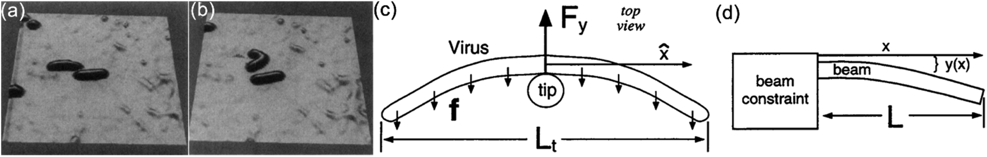
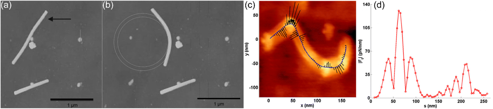
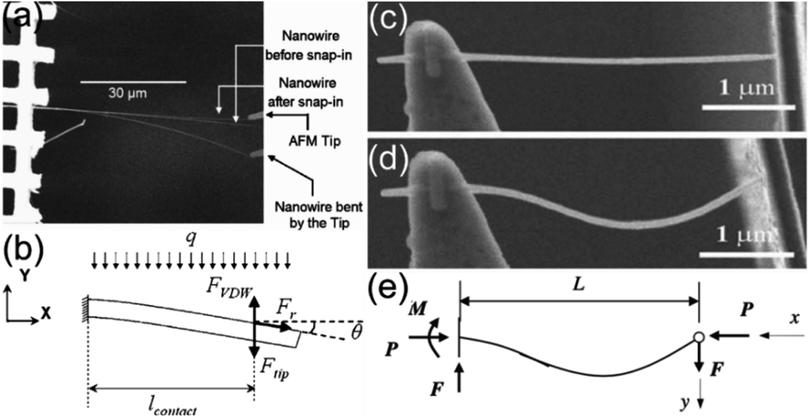
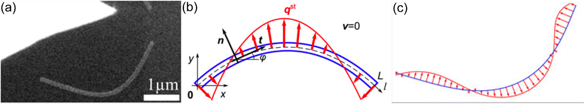
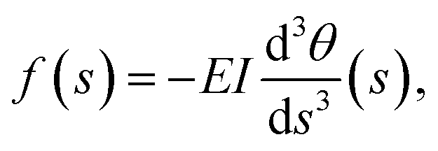
Although direct AFM measurement strategies have yielded some remarkable results, and the detailed techniques of the measurement have seen significantly improvement, they remain time-consuming and inaccurate. This is attributed to the complex mechanical relationship involving contact forces and contact areas among the AFM-tip, the targeted 1D materials, and the supporting substrate. Consequently, simpler indirect measurement strategies have been developed. Falvo et al. initially proposed an indirect strategy to measure the frictional force between an individual 1D virus and a supporting substrate by using AFM-based nanomanipulation.171 In this method, they manipulated an initially straight individual 1D virus on a graphite substrate, and bent it into arc shape, as illustrated in Fig. 10(a) and (b). By using the small deflection cantilever beam model with one end fixed, as shown in Fig. 10(c) and (d), the interfacial frictional shear force per unit length between the 1D virus and graphite substrate was estimated to be 5 mN m−1 by using eqn (1),| |  | (1) |
where, qn is the lateral static friction per unit length acting on the 1D virus, E and I are the Young's modulus and second moment of inertia of the 1D virus, y(x) is the deflection of the longitudinal deflection of the virus cantilever.
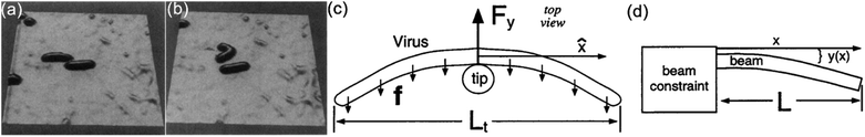 |
| | Fig. 10 (a and b) AFM images of the tobacco mosaic virus on graphite before and after AFM manipulation, respectively. (c and d) Schematic illustrations of the mechanical model for calculating frictional forces between a virus and a graphite substrate. Reproduced with permission.171 Copyright 1997, Elsevier. | |
Subsequently, Bordag et al. applied this indirect strategy to further measure the static friction between NWs and substrates, showcasing significant improvements and extensions in AFM-based nanomanipulation.172 In their experiment, an initially straight InAs NW attached to a SiO2 substrate was manipulated to its most bent state using an AFM tip, as illustrated in Fig. 11(a) and (b). Once equilibrium was reached between the static friction and the elastic restoring force of the bent NW, the static friction could be indirectly determined from the bending curvature of the NW, based on the elastic beam theory, Bordag et al. derived a simple equation,172
| |  | (2) |
where
k is curvature of the bend profile of the NW, to calculating the static friction force. Consequently, the average shear frictional force per unit area of 0.99 ± 0.25 MPa was estimated for the InAs NWs on Si substrates by using
eqn (2).
172
 |
| | Fig. 11 (a and b) AFM micrographs of InAs NWs on SiO2 substrate before and after manipulation, respectively. The black arrow in (a) denotes the force vector to be applied to the NW, and the circles in (b) are the inner and outer curvature radii. Reproduced with permission.172 Copyright 2007, Wiley. (c) AFM image of a SWCNT manipulated into an S shape. The arrows in (c) are the frictional forces act on the SWCNT to prevent it from returning to its undeformed position. The forces have been normalized by the maximum frictional force per unit length. (d) Friction force distributions along the length of SWCNT. Reproduced with permission.173 Copyright 2009, IOP. | |
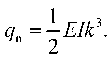
Although the new indirect strategy is simple and can significantly reduce the effect of the contact uncertainties from the direct AFM measurement,173–175 it was found that the proposed mechanical models are overly simplified, which might lead to significant errors in certain practical calculations. To achieve a more complete and accurate description, some more sophisticated mechanical models were developed for the calculation of the static friction distribution along the whole 1D materials.133,173,175–181 For example, Strus et al. considered the bending of the 1D material as a pure bending state, found that the normal static friction force along the 1D material could be expressed as,173
| |  | (3) |
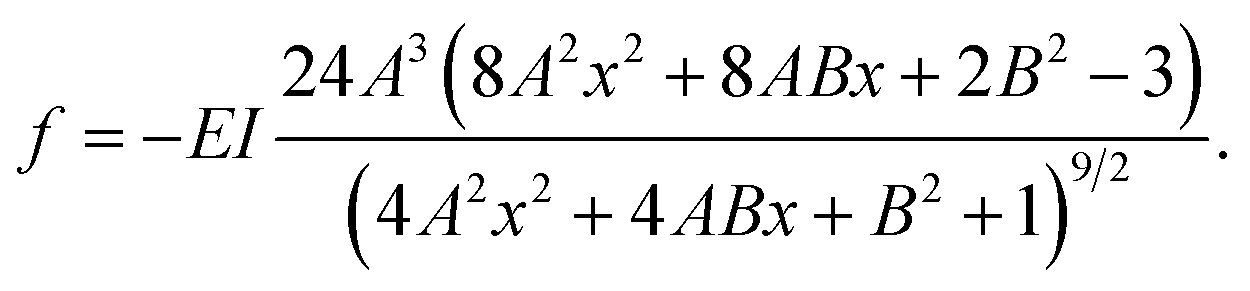
Based on this model, Strus et al.173 investigated the interfacial friction force distribution along the length of a supported SWCNT, which was manipulated into various shapes on the Si substrate using AFM, as illustrated in Fig. 11(c) and (d). Later on, Stan et al. proposed another route to calculate the static friction force along the NW, by fitting the NW skeleton using a parabola in the form, y = Ax2 − Bx + C. In terms of the coefficients A, B, and C of the fitting parabola, the local friction force per unit length could be obtained by,175
| |  | (4) |
Fig. 12 depicts the AFM image of a Si NW manipulated in the most bent state by the AFM tip as well as the static friction force along NW calculated by using eqn (4).
 |
| | Fig. 12 (a) The most bent segment of a Si NW hook. The bending stress profile along the white middle line of the NW is shown. (b) The friction force per unit length necessary to balance the elastic forces in the bent NW. The length and orientation of the line segments give the amplitude and direction of the friction force from outside and inside of the hook toward the NW. (c) The profile of the friction force per unit length, f, shear force, V, and bending moment, M, as a function of distance, s, along the NW. Reproduced with permission.175 Copyright 2012, Springer Nature. | |
As indirect measurement strategies are considerably simpler in experiments compared to direct strategies, and can significantly reduce uncertainties associated with the complex contact relationships in the direct approaches, many researchers have employed these indirect strategies for further studies on the frictional behaviors between 1D materials and substrates, each yielding commendable results.133,175–181 Nevertheless, it is crucial to emphasize that indirect measurement strategies relying on eqn (1)–(3) exhibit significant sensitivity to the bending profile of the targeted 1D materials. Importantly, the approximate treatment of boundary conditions for the derivation of eqn (2) and (3) could introduce considerable inaccuracy in actual measurements, likely contributing to the extremely high static friction stress values, approximately two orders of magnitude higher compared to the kinetic friction stress, reported in certain earlier studies.176–178
3.1.3. Achievements and challenges in AFM-based measurements techniques.
Direct measurement strategies have been employed to investigate frictional behavior, entailing the manipulation of 1D materials with an AFM tip to gain insights into sliding and rolling behaviors. Concurrently, researchers have introduced innovative manipulation techniques, such as attaching MWCNT to AFM tips or utilizing AFM-based nanomanipulation, facilitating controlled experiments to comprehend the distinctive frictional properties of individual 1D materials. The broad applicability of AFM-based measurements is demonstrated through the exploration of diverse material systems, including CNTs, ZnO NWs, and Si NWs. In addressing the limitations of direct measurements, advancements in indirect measurement strategies have emerged, involving the manipulation of 1D material's shape and estimation of frictional forces based on resulting deformations, offering a simpler and potentially more accurate alternative. AFM-based measurements have the potential to explore the dependences of the frictional behaviors of 1D materials on the testing and environmental parameters, including relative humidity, temperature, normal loading, sliding velocity, and interface potential difference. This not only significantly improves our understanding of the frictional behaviors of 1D materials but also contributes to the design and applications of micro/nano devices based on the friction of 1D materials.
However, due to their inherent characteristics, AFM measurements also unavoidably confront some inevitable issues and challenges. (a) Lack of real-time direct visual feedback: AFM cannot provide real-time direct visual feedback and can only monitor the initial and final states of the dynamic testing process. This “blind manipulation” characteristic not only severely impacts testing efficiency but also introduces considerable uncertainty in actual measurements. For example, lateral forces measured by AFM may originate from interactions between the AFM tip and 1D materials, between 1D materials and the substrate, or between the AFM tip and the substrate, making it challenging to differentiate.182–185 Additionally, the frictional forces experienced by flexible 1D materials during movement on the substrate, especially static frictional forces, are often non-uniform along the length direction of the 1D materials. As AFM measurements lack real-time visual characteristics, complex mechanical models must be used for derivation, potentially leading to significant errors in the obtained results.176–178 Moreover, distinguishing between sliding and rolling of 1D materials on the substrate remains a challenge.136,138 (b) Unpredictable deformations and damages: friction forces between 1D materials and the substrate are often substantial, and the sharp AFM tip used in manipulation and measurement processes may cause deformations or damages on the sample surface. The tip itself may undergo significant deformations or damages, affecting the final measurement accuracy and reliability.186,187 The experimental results for 1D materials obtained by AFM-based methods are outlined in Table 1.
Table 1 List of experimentally determined frictional properties of 1D materials with substrates and between two individual 1D materials measured by AFM-based techniquesa
| Techniques |
Interfaces |
Friction parameters |
Notes |
Ref |
f
s: Static friction force, fk: kinetic friction force, qs: static friction force per unit length, qk: kinetic friction force per unit length, σs: static shear stress or strength, σk: kinetic shear stress or strength, µs: static shear coefficient, µk: kinetic shear coefficient, L: length, A: contact areal, ![[D with combining macron]](https://www.rsc.org/images/entities/i_char_0044_0304.gif) : average diameter, R: radius, T: temperature, RT: room temperature, RH: relative humidity, The notations such as “rectangular, hexagonal, circular” written in the list of notes, represent the cross-sectional shapes of 1D materials. : average diameter, R: radius, T: temperature, RT: room temperature, RH: relative humidity, The notations such as “rectangular, hexagonal, circular” written in the list of notes, represent the cross-sectional shapes of 1D materials.
|
| AFM-direct measurement |
MWCNT-graphite substrate and mica |
q
k = 0.006 nN nm−1; σk = 2 MPa |
R = 13.5 nm; L = 590 µm; A = 7 nm2; ambient |
136
|
| AFM-direct measurement |
MWCNT-mica |
— |
L = 20–500 nm; ambient |
168
|
| AFM-direct measurement |
MWCNT-SWCNT |
µ
k = 0.006 ± 0.003 MPa; σk = 4±1 MPa |
D
1 (MWCNT) = 75 nm; D2 (SWCNT) = 1.43 nm; L1 (MWCNT) = 0.88 µm; A = 0.9 nm2; T ≈ 21 ± 1 °C; RH ≈ 30 ± 5% |
169
|
| AFM-direct measurement |
MWCNT-SWCNT |
µ
s = 0.2; σs = 1.4 GPa |
D
1 (MWCNT) = 70 nm; D2 (SWCNT) = 1.43 nm; A = 0.85 nm2; T ≈ 21 ± 1 °C; RH ≈ 30 ± 5% |
170
|
| AFM-direct measurement |
MWCNT-Si tip |
σ
k (longitidunal) = 0.5Gpa; σk (transversal) = 0.845–1.781 GPa |
D = 4–12 nm; RT |
137
|
| AFM-direct measurement |
ZnO NW-Si substrate |
f
s = 69.3 nN; fk = 36.4 nN; µs = 462; µk = 242 |
D = 67 nm; L = 0.95 µm; T ≈ 25 °C; RH ≈ 30% |
138
|
| AFM-manipulation |
MWCNT-hydrogenated Si surface |
σ
k = 10 MPa |
A = 5 × 10⁻¹⁶ nm2 |
188
|
| AFM-indirect measurement |
Tobacco mosaic virus-graphite |
q
s = 5 mN m; σs = 1 MPa |
Shell, D1 (outer) = 18 nm; D2 (inner) = 5 nm; L = 0.3 µm; ambient conditions; RH ≈ 30% |
171
|
| AFM-indirect measurement |
MWCNT-Si substrate |
f
k = 5 nN; σk = 10 MPa |
D = 39–123 nm; A = 5 × 10⁻¹⁶ nm2 |
189
|
| AFM-indirect measurement |
InAs NW-SiO2 substrate |
q
s = 28 pN nm; σs = 0.99 MPa |
Hexagonal; D ≈ 50 nm; L ≈ 3 µm |
172
|
| AFM-indirect measurement |
SWCNT-SiO2 substrate |
q
s = 230 pN nm−1 |
D = 1.6 nm; L = 0.265 µm; ambient; RH ≈ 30% |
173
|
| AFM-indirect measurement |
InAs NW-Si3N4 substrate |
— |
D = 20–80 nm; L = 3–4 µm; T ≈ 17 °C; RH ≈ 24% |
176
|
| AFM-indirect measurement |
InAs NW-Si3N4 substrate |
— |
D = 40–70 nm; L = 3–4 µm; T ≈ 17 ± 0.5 °C; RH ≈ 24 ± 3% |
178
|
| AFM- indirect measurement |
InAs NW-SiO2;InAs NW-silanized SiO2; InAs NW-Si3N4 substrate |
— |
D = 20–80 nm; L = 3–4 µm; T ≈ 17 ± 0.5 °C; RH ≈ 24 ± 3% |
177
|
| AFM- indirect measurement |
SiO NW-Si substrate |
q
s = 0.15–0.68 N m−1 |
Circular; D = 120–140 nm; L ≈ 1.18–2.55 µm; T ≈ 25 °C; RH ≈ 40% |
179
|
| AFM- indirect measurement |
Oxidized Si NW-SiO2 substrate; oxidized Si NW-graphene substrates |
σ
k (on SiO2) = 7.5–12.3 MPa; σk (on graphene) = 4.7–7.0 MPa; qs (on SiO2) = 0.04–0.12 N m−1; qs (on graphene) = 0.034–0.09 N m−1; qk (on SiO2) = 0.034–0.07 N m−1; qk (on graphene) = 0.02–0.054 N m−1 |
Circular; D = 42–178 nm; L = 0.85–11.2 µm; T ≈ 25 °C; RH ≈ 40% |
180
|
| AFM-manipulation |
Ag NW-SiO2/Si substrate |
µ
s = 0.03; µk = 0.015 |
D ≈ 65 nm; L = 0.8 µm; T ≈ 20–25 °C; RH ≈ 30–40% |
133
|
| AFM-manipulation |
Ag NW-graphite substrate; Ag NW-MoS2 substrate |
f
s (on graphite) = 36.7 ± 1.8 nN; fs (on MoS2) = 23.2 ± 1.2 nN |
Cylindrical; D = 60 nm; L (on MoS2) = 1.2 µm; L (on graphene) = 1.0 µm; T ≈ 20–25 °C; RH ≈ 30–40% |
190
|
| AFM- manipulation |
Ag NW-SiO2 substrate |
q
s = 1.07 N m−1; qk = 0.56 N m−1 |
D = 50 nm |
191
|
3.2. SEM based measurements
The necessity for precise real-time visualization in the investigation of interfacial forces at the nanoscale has driven the integration of SEM into the examination of the frictional properties of 1D materials. Currently, the incorporation of SEM with advanced manipulation and force-sensing techniques, provided a powerful method, specifically in situ SEM nanomanipulation, for the real-time characterization of the frictional behavior of 1D materials in a visualization mode.
3.2.1. Indirect measurement strategies based on SEM manipulation.
In 2007, Desai et al. firstly used this strategy for observing the interfacial friction and adhesion of NWs.192 As shown in Fig. 13(a), one end of the targeted ZnO NW was fastened at the edge of a TEM Grid, the Si AFM tip, moistened on the manipulator arm, was attached to the end of the NW to deflect. Based on the mechanical model can be represented in Fig. 13(b), the bending profile of the NW could be described by using,192| | 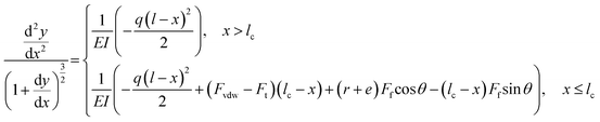 | (5) |
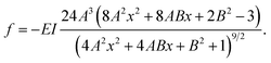
where l and lc are the total and force acting lengths of NW respectively, q is the force per unit length induced by ion-beam, Fvdw and Ff are the vdW adhesion force and friction force between Si AFM Tip and ZnO NW respectively, Ft is extracted force by AFM tip, and θ is the slope angle. According to eqn (5), a friction force of 7.7 nN between the NW and AFM tip was obtained by numerically solving eqn (4).192
 |
| | Fig. 13 (a) NW snap in due to the adhesion from the AFM tip (three different stages of NW loading are superimposed), (b) mechanical model for calculating forces acting on the NW in (a). Reproduced with permission.192 Copyright 2007, AIP. (c and d) SEM images of an individual NW before buckling and after buckling and just prior to sliding on the right end, respectively. (e) Mechanical model for calculating forces acting on the NW in (d). Reproduced with permission.193 Copyright 2010, Springer Nature. | |
In 2010, Zhu et al. reported the experimental measurement on the frictional shear stress of ZnO and Ag NWs over Au substrate using the in situ SEM manipulation strategy. In their experiment, an initially straight NW affixed to a tungsten (W) tip underwent buckling when the W tip was pushed from a manipulator arm towards an Au substrate, as shown in Fig. 13(c) and (d). As the loading on the NW increases, the NW undergoes buckling until it reaches the point of sliding. Applying the buckling theory with one end fixed and the other end pinned, the friction force on the NW could derived from the bending profile of the NW using the following equation,
| |  | (6) |
where
P and
F are the normal and friction forces, respectively, as depicted in
Fig. 13(e). In their study, the friction coefficients and shear strengths between Ag NWs and Au substrates, ZnO NWs and Au substrates as 0.09–0.12, 134–139 MPa, 0.1–0.15 and 78.9–95.3 MPa were obtained by numerically solving
eqn (6).
193
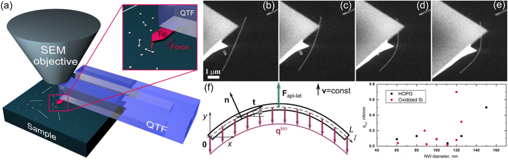
The methods proposed by Desai et al.192 and Zhu et al.193 presented a novel perspective for investigating the interfacial frictional behavior of 1D materials on substrates. However, both methods employed relatively intricate mechanical models requiring numerical solutions and, notably, did not explicitly differentiate between static and kinetic forces. Subsequently, Polyakov et al. developed a nanomanipulation techniques based on an in situ SEM strategy for visual observation and perform a comprehensive characterization on the frictional behavior of 1D NWs over substrates.132,144,194–197 In their study, the 1D materials on substrates were manipulated by an AFM tip glued to a quartz tuning fork (QTF), which is driven by a 3D nanomanipulator inside the SEM, as depicted in Fig. 14(a). The friction forces on the targeted NWs could be derived from the lateral forces recorded by the AFM tip or from the bending NW profiles using the Timoshenko beam theory. Fig. 14(b)–(e) shows the SEM images of an NW pushed to slide along the HOPG substrate by AFM tip with constant velocity.197 After sliding a few microns, the NW curved into an arc shape with a distinct curvature, attributed to the equilibrium maintained between NW-substrate kinetic friction and internal elastic forces within the NW. According to these equilibrium conditions shown in Fig. 14(f), the bending shape of the NW could be described by,197
| | 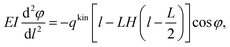 | (7) |
where
φ is the tangent angle function of the NW axis
l,
qkin is the distributed kinetic force on the length,
H(
x) is Heaviside step function. Consequently, by numerically solving
eqn (7) with initial condition
φ′ = 0, the kinetic friction per unit length 0.04–0.5 nN nm
−1 for ZnO NWs on HOPG substrate and 0.03–0.7 nN nm
−1 for ZnO NWs on Si substrate, as depicted in
Fig. 14(f).
197
 |
| | Fig. 14 (a) Experimental scheme of the nanomanipulation of NW with AFM tip glued inside the AFM tip QTF inside the SEM. Reproduced with permission.198 Copyright 2015, IOP. (b–e) SEM images of a ZnO NW on the HOPG pushed to slide by the AFM tip from the initial to final shape. (f) Mechanical model for calculating the kinetic frictional force on the NW, and kinetic frictions measured as a function of NW diameter on HOPG and oxidized Si wafer. Reproduced with permission.197 Copyright 2012, Wiley. | |
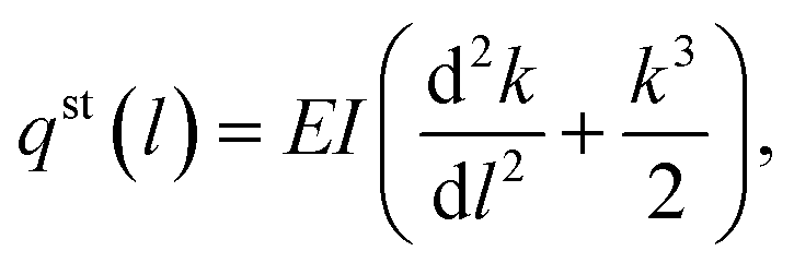
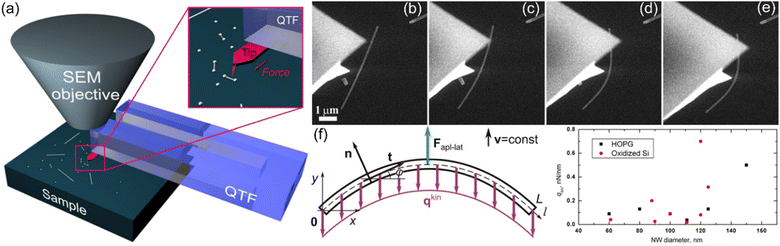
In their above mentioned technique,197 even after the external force is extracted, Polyakov et al. found that, after removing the external force, the bent NW usually spring back slightly and would find a new balance shape due to the elastically restored force and the static frictional force from the substrate (Fig. 15). By neglecting the tangential component of static friction, they obtained,195
| |  | (8) |
for calculating the static friction on NW with the boundary conditions, d
k/d
l|
l=0 = d
k/d
l|
l=L = 0 and
k|
l=0 =
k|
l=L = 0, where
k and
qst(
l) are the curvature and the static frictional force along the NW, respectively. Based on
eqn (8), it was found that the static friction force per unit length is between ZnO NW-Si substrate is 1.7–2.34 nN nm
−1, very close to their kinetic friction force 1.8 nN nm
−1.
 |
| | Fig. 15 (a) SEM image of a bent ZnO NW lying on a substrate. (b) Schematics of the expected static friction force distributed along a bent NW. (c) Distribution diagram of static friction along the NW in (a) obtained from eqn (7). Reproduced with permission.195 Copyright 2012, Springer Nature. | |
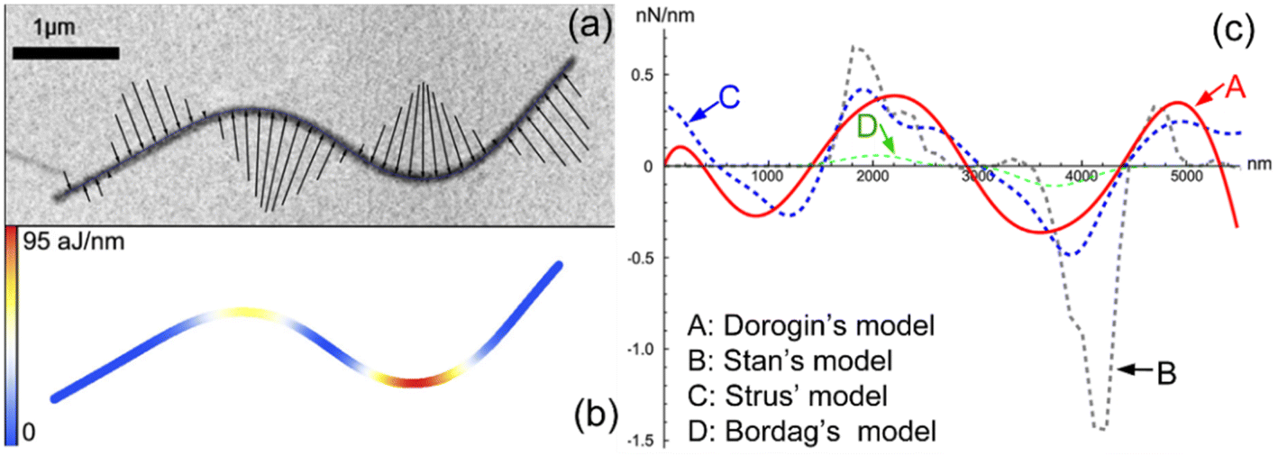
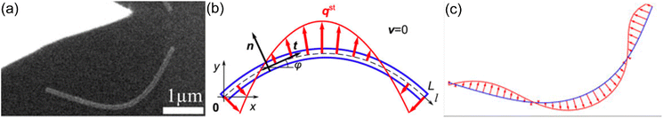
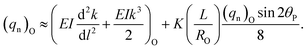
To evaluate the reliability of the mechanical models suggested for calculating the static friction along bent NWs based on their bending profiles, Antsov et al. performed a direct comparison in 2014. In their study, a ZnO NW on SiO2 substrate was manipulated into a complex shape, as shown in Fig. 16(a), by using the AFM tip in SEM chamber. Subsequently, the static friction force along the bent NW was calculated using the mechanical models described by eqn (2),172(3),173(4),175 and (8),194,195 respectively. As can be seen from the comparative results in Fig. 16(c), it seems like the mechanical model suggested by Dorogin et al. provided a more accurate description for NWs with more intricate bending shape. This is presumed to be attributed to the consideration of the conditions at the free end in Dorogin's model.199 However, it should also be noted that all these models neglected the tangential component of the frictional force along the NW, which could result in noticeable inaccuracies in actual calculations. For instance, the frictional force at the end of a bent NW is generally assumed to experience the highest static frictional force from the substrate, as the end is expected to have the maximum tendency to slide on the substrate. Nevertheless, as observed in Fig. 16(a), the friction forces at the free ends are considerably lower than the maximum frictional forces.
 |
| | Fig. 16 (a) SEM image of the bent ZnO NW held by the static friction from the substrate. The rows showed the normal component of static friction force. (b) Numerically calculated elastic energy. (c) Static friction forces distributions along NW using different models. Reproduced with permission.199 Copyright 2014, Elsevier. | |
3.2.2. Direct measurement strategies based on SEM manipulation.
As the manipulation force on the NW could be directly recorded by the pre-calibrated QTF force sensor installed inside the SEM (see Fig. 14(a)), Polyakov et al. first detected directly the lateral force for the sliding of ZnO NW on Si substrate as depicted in Fig. 17(a)–(e), and obtained the average frictional shear stress of 2.1 ± 0.26 MPa. Subsequently, Polyakov et al. comparatively studied the kinetic behavior and tribological properties of Ag, Au, and Cu nanodumbbells on a SiO2 substrate. As seen in the typical SEM images extracted from the recorded video of the manipulation process shown in Fig. 17(f)–(j),198 the nanodumbbell rotated around one of its ends (kinetic friction) at a force of 10–20 nN, after overcoming the static friction force of ∼500 nN. During the in situ measurement, the static and kinetic friction typically exhibited a significant difference, presumed to be closely related to the so-called “contact aging” phenomenon at the nanoscale. Moreover, in their manipulation experiment, the nanodumbbells exhibited several regimes of motion (sliding, rolling, and rotation). Sliding (translation) was observed in very rare cases. Rolling of a nanodumbbell onto the other side was observed more frequently. The most common scenario was the rotation of the nanodumbbell around one of its end bulbs.
 |
| | Fig. 17 (a–d) SEM images of the suspended NW being pushed by the tip. (e) The corresponding force curve. Reproduced with permission.194 Copyright 2011, Elsevier. (f–i) SEM images for the manipulation process of an Ag nanodumbbell. (j) The corresponding recorded tip–nanodumbbell interaction force. Reproduced with permission.198 Copyright 2015, IOP. | |
Note that the NW-substrate friction force is usually quite higher, it is therefore needs a high preload force on the AFM tip to manipulation the NW. This usually leads to the unexpected damages on the targeted NW, and especially results into significantly uncertainties in the actual testing process.200 As result, Gao et al. developed a new technique based on the force feedback characteristics of force sensor to eliminate the effects of preload on the measurement. Using the new testing technique, they found that the friction shear stress between Si NWs and SiC substrate is 1.05 ± 0.32 MPa.201
3.2.3. Achievements and challenges in SEM-based measurements.
The development of techniques for measuring friction forces in 1D materials using SEM has evolved from the early stages of observations and measurements of sliding and total friction forces. From the development of by using in situ SEM manipulation method to evaluate frictional behavior to sensor integrated method. It has advanced to incorporate more sophisticated measurements, including static friction transition to kinetic friction, pure kinetic friction, and the relaxation from kinetic friction to self-equilibrium static friction forces. Additionally, these techniques now allow for the observation of various frictional processes, such as rolling, sliding, and rotating (currently only available for large aspect ratio NWs). This progress has significantly enhanced the capabilities of these methods, providing exceptional real-time observational insights.
However, certain challenges and issues still persist. SEM operates under high vacuum conditions, making it impractical to assess the impact of relative humidity, which has been shown to significantly alter the frictional behavior of 1D materials. Moreover, the high-energy electron beam used in SEM may impact the interfacial frictional properties of 1D materials in several ways: (i) inducing changes in the sample's morphology, potentially deviating from its native state;202 (ii) generating electrostatic attraction forces that interfere with precise friction force measurements; (iii) triggering chemical reactions, altering the interfacial composition and influencing observed frictional behavior;203,204 and (iv) inducing residual stress in 1D NWs being tested and altering the accuracy of the indirect measurement strategies.192 In addition, the manipulation of 1D materials in SEM processes potential obstacles, including the impact of manipulator vibration199,205–209 and the preload200 of the manipulation tip, both may affect the result accuracy.
Finally, it should also be noted that while the in situ SEM manipulation strategy enhances visibility during the manipulation of 1D materials, it falls short in fully revealing the contact interface between NWs and substrates. In this regard, TEM may provide a solution for detecting the contact interface during sliding. For example, in 2003, Fujisawa and Kizuka pioneered a groundbreaking technique by combining AFM with TEM and STM (scanning tunneling microscopy). This innovative approach allows for the simultaneous observation of a TEM movie capturing the AFM/STM tip apex and sample surface with the AFM force signal and STM current signal. They witnessed the lateral sliding of the Cu tip on the Cu surface when the sample underwent displacements perpendicular to the surface. This implies that the AFM data, including the cantilever deflection, results not only from a force component acting perpendicular to the surface but also from a force component parallel to the surface.187 In 2012, Sato et al. developed an electrostatically driven MEMS system operating within a TEM specimen chamber, allowing for precise sub-nanometer actuation, studied the Ag–Ag asperity friction.210 In 2021, Shan et al. studied the single asperity friction between Ag cantilever and W substrate by in situ TEM manipulation.211 In 2022, He et al. used AFM/TEM combined techniques conducted experiments on single asperity between W tip and Au substrate.212 These studies offered an opportunity for the direct observation of the interfacial contact at the nanoscale. However, the current scope of these investigations is restricted to the examination of individual asperities due to the severely limited observation range. This limitation currently hinders the ability to observe the distribution of frictional forces along the length of 1D materials. The experimental results of 1D materials measured using SEM based techniques are presented in Table 2.
Table 2 List of experimentally determined frictional properties of 1D materials with substrates measured by SEM-based techniquesa
| Techniques |
Interfaces |
Friction parameters |
Notes |
Ref |
|
q
com: Static-kinetic combined friction force, σcom: static-kinetic combined shear stress, qmaxs: maximum static force per unit length, σmaxs: maximum static shear strength, bar “—”: average values.
|
|
In situ SEM manipulation |
ZnO NW-Si substrate |
f
s = 7 nN |
EI = 29.7 pN µm−1 |
192
|
|
In situ SEM manipulation |
Ag NW-Au substate; ZnO NW-Au substate |
µ
ZnO–Au = 0.1–0.15; µAg–Au = 0.09–0.12; σZnO–Au = 78.9–95.3 MPa; σZnO–Au = 134–139 MPa |
A
ZnO–Au = 217–387 nm2; AAg–Au = 240–288 nm2 |
193
|
|
In situ SEM manipulation |
ZnO NW-oxidized Si wafer |
![[q with combining macron]](https://www.rsc.org/images/entities/i_char_0071_0304.gif) k = 0.2 ± 0.08 nN nm−1; σk = 2.1 ± 0.26 MPa
k = 0.2 ± 0.08 nN nm−1; σk = 2.1 ± 0.26 MPa |
Hexogen; D = 160 nm; L = 3.9 µm |
194
|
|
In situ SEM manipulation |
ZnO NW-Si wafer |
q
s = 1.7–2.4 nN nm−1; qk = 1.8 nN nm−1 |
— |
195
|
|
In situ SEM manipulation |
ZnO NW-oxidised Si wafer |
q
maxs ≈ 11 nN nm−1; s ≈ 5 nN nm−1; qk ≈ 0.25 nN nm−1; σmaxs ≈ 195 MPa; σk ≈ 65 MPa; σk ≈ 2.8 MPa |
Hexogen; D = 70–150 nm; L = 10–20 µm |
144
|
|
In situ SEM manipulation |
ZnO NW-oxidised Si wafer; ZnO NW-HOPG substrate |
q
com (on Si) = 0.12–16 nN nm−1; qcom (on HOPG) = 0.04–7.5 nN nm−1; qk (on SiO2) = 0.04–0.5 nN nm−1; qk (on HOPG) = 0.03–0.7 nN nm−1; σc (on SiO2) = 36 MPa; σc (on HOPG) = 24 MPa; σk (on Si) = 3.2 MPa; σk (on HOPG) = 2.75 MPa |
Hexogen; D = 60–160 nm ( = 110 nm) |
132
|
|
In situ SEM manipulation |
ZnO NW-Si substrate |
σ
k = 1–60 MPa |
Hexogen; few tens to a few hundreds of nm; several hundred nm to a few µm |
213
|
|
In situ SEM manipulation |
Ag ND-SiO2 wafer |
f
s = 500 nN; fk = 10–20 nN |
— |
198
|
|
In situ SEM manipulation |
SiC NW-Si substrate |
σ
k ≈ 1.05 ± 0.32 MPa |
— |
201
|
|
In situ SEM manipulation |
MWCNT–MWCNT |
σ
s ≈ 0.3 MPa; σk ≈ 0.09 MPa |
D = 60 nm; L = 7.5 µm |
214
|
3.3. OM-based measurements
Although the resolution of OM is typically above 200 nm, people discovered long ago that through OM, it is possible to “see” individual NFs with diameters well below 100 nm. Attempts were made to directly achieve and conduct nanomanipulation using NF materials under an OM.215 It is precisely based on the special imaging features of NFs under an OM that, in the past two decades, researchers have gradually established nanomanipulation techniques based on OM. These techniques are employed to manipulate individual NFs and characterize their various properties. In particular, this OM-based nanomanipulation method has become one of the primary approaches for systematically characterizing the mechanical behavior and surface mechanical properties of NFs, through the combination with external manipulators, MEMS, or force/displacement sensors, and other micro-nano devices.126,139,142,183,216–222
3.3.1. Direct OM-based measurement strategies.
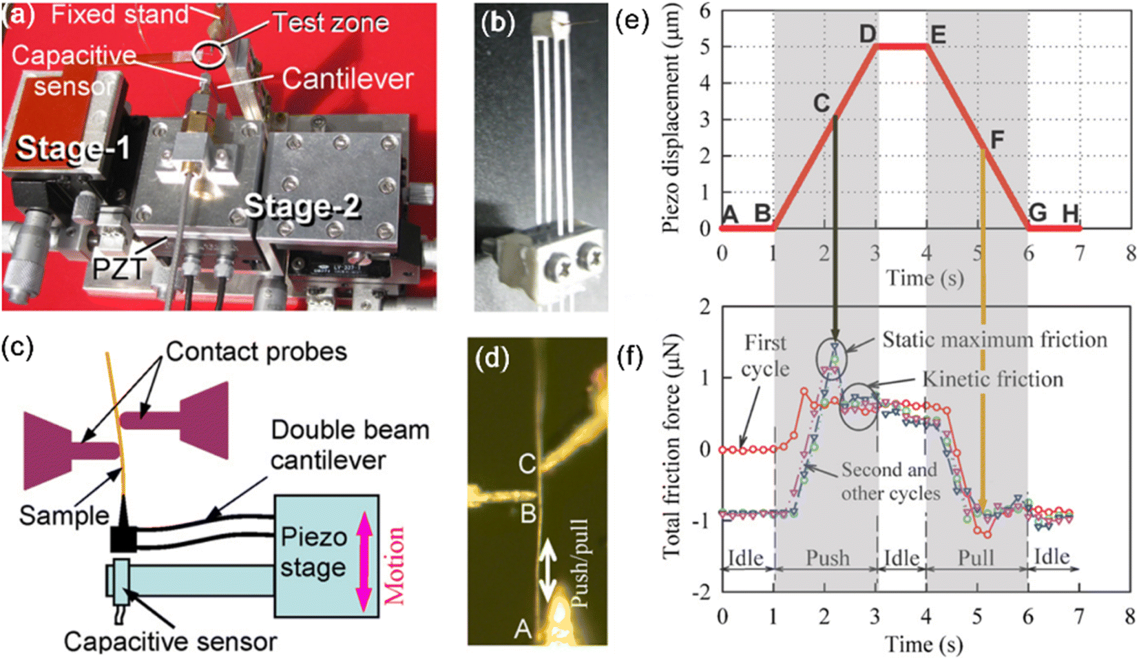
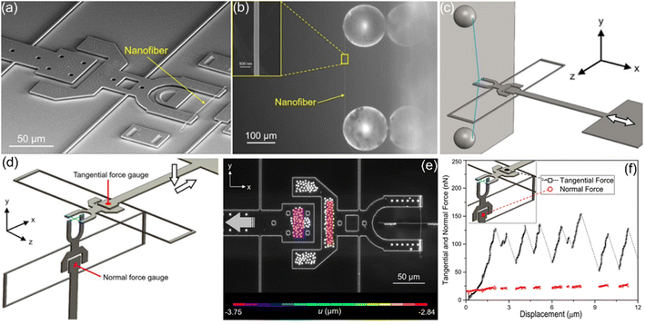
Manoharan et al. pioneered the development of custom adhesion-friction force sensor to directly measure the adhesion-friction force of the NW-substrate interface under OM with zero applied normal load. In their experiment, the force sensor was mounted on a piezoelectric actuator with a travel of 100 µm in the x, y and z directions. The ZnO NW sample was fastened at the end of the cantilever of the force sensor using focused ion beam deposited platinum, as depicted in Fig. 18(a). A Si wafer used as the substrate was placed on a manual manipulator with 1 µm positioning accuracy, and a minimum of 0.5 µm positioning resolution can be achieved with an OM using a 100× long working distance objective, as shown in Fig. 18(b). The adhesion-friction force sensor has a U-shaped spring for friction force measurement and a cantilever beam as shown in Fig. 18(c) and (d). When the NW shears on the substrate, the displacement of the friction force spring can be directly measured by recording the extension of the reference gap. Fig. 18(f) presents the typical friction loading and unloading curve for a ZnO NW on Si substrate under ambient conditions. They estimated that the frictional shear stress between ZnO NW and Si substrate was ∼1 MPa.125
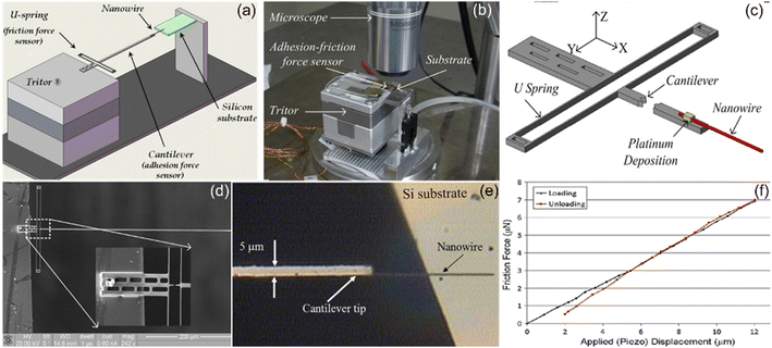 |
| | Fig. 18 (a) Experimental setup diagram showing the nanosize force sensor oriented on a Tritor® piezo-actuator and the Si substrate (not up to scale). (b) Experimental setup under a 100× OM objective. (c) Force sensor (not up to scale) diagram and (d) the corresponding SEM image of the force sensor (inset: zoomed view of the displacement markers). (e) OM image of the NW positioned on the substrate with the intended contact length. (f) Friction loading and unloading curve of ZnO NW on Si substrate under ambient conditions. Reproduced with permission.125 Copyright 2009, IOP. | |
In 2009, Akanda et al. proposed a novel direct measurement method by using a two-manipulator system with two force sensors, enabling direct visual observation at atmospheric environment under OM. Illustrated in Fig. 19(a)–(d), the force sensor adopts a four-legged parallel beam structure, offering precise measurement of friction and normal contact forces under high-resolution digital microscope observation. Manipulator 1 serves the purpose of transporting test samples or micro-probes, while manipulator 2 hosts a micro-force sensor connected to a piezoelectric platform. In the experiment, the Pt microwire could be pushed and pulled in normal contact between two closely placed W probes, and the push/pull forces are directly recorded at specific speeds controlled by a computer-controlled piezoelectric platform. Fig. 19(e) illustrates a typical cycle of push/pull motion at a speed of 2.5 µm s−1. The push/pull motion, performed for a given speed and deformation at B shown in Fig. 19(d), is repeated for several cycles. The push/pull forces recorded for the first four consecutive cycles are presented in Fig. 19(f) as a function of time. The static and kinetic friction coefficients, 0.25 and 0.2 between the Pt wire and W tip, were calculated based on the normal force and friction force.223
 |
| | Fig. 19 (a) Experimental setup for the two-manipulator system. (b) Four-legged parallel beam cantilever. (c) Schematic of friction force measurement system. (d) Optical micrograph of two W probes and the targeted Pt wire. (e) The push–pull cycle of the wire against the probes, corresponding to the piezo displacement during friction measurement, and (f) frictional forces recorded at various cycles. Reproduced with permission.223 Copyright 2011, Elsevier. | |
In 2020, Das et al. introduced an innovative MEMS-based system dedicated to precisely measuring adhesion and friction forces in 1D materials.224 The testing process involved utilizing digital image correlation (DIC) on high-magnification OM images, enabling the accurate calculation of relative motion within the MEMS components, and consequently, the determination of applied forces on the fibers with an impressive resolution of approximately 2 nN, as illustrated in Fig. 20. In the experiment, two segments of Polyacrylonitrile (PAN) from the same fiber was isolated using a manipulator. One segment was securely placed across a 50 µm section of the MEMS device, while the other was affixed across two glass beads using a two-part epoxy, as depicted in Fig. 20(a) and (b), respectively. Fig. 20(c) and (d) provide the schematics of the normal and shear detachment testing procedure, encompassing the contact of midpoints of two orthogonal fibers, the establishment of an adhesive connection, and subsequent detachment. For shear detachment test, two PAN fibers were attached to two MEMS devices and brought into contact by translating along the y-axis using a piezoelectric actuator and detached them in shear mode by translating the top MEMS device along the x-axis with a second piezoelectric actuator. They continuously monitored the entire experimental process of each MEMS device using a dedicated high-resolution OM/CCD camera system. Fig. 20(e) depicts the top view of a transverse sliding experiment, showcasing DIC-derived rigid body U – displacements of two components of the MEMS force sensor superimposed directly onto the image. The relative displacement of these components, when multiplied by the spring constant of the device, yielded the tangential force applied during transverse sliding. In their test, the stick-slip detachment behavior between NFs was identified, as indicated in Fig. 20(f). Moreover, the interfacial shear adhesion strength is shown to be constant for a broad range of contact radii (25–140 nm) and approximately equal to the material shear stress at yielding. It is therefore suggested that the shear yielding might be the controlling mechanism for the shear detachment of individual polymer NFs interacting with vdW adhesion.
 |
| | Fig. 20 (a) PAN NFs mounted onto a MEMS device. (b) NF mounted between two glass beads. Inset: SEM micrograph of the PAN NF, showing the uniform diameter along its length. (c and d) Schematic of the normal and shear detachment test, respectively. The fibers are shown in blue color. (e) The top view of a part of the MEMS testing device, along with the two intersecting fibers on the right side, used in a shear experiment. The rigid body U-displacements of two components of the MEMS device, calculated through DIC, are superimposed onto the bottom. (f) Tangential and normal forces curve as the function of the displacement. The tests were conducted at a crosshead speed of 12 nm s−1. Reproduced with permission.224 Copyright 2020, Elsevier. | |
3.3.2. Indirect OM-based measurement strategies.
Integrating sensors or MEMS with OM manipulation techniques for directly measuring the interfacial friction forces of 1D materials provides a powerful tool for studying the frictional behavior of 1D materials. However, such direct measurement strategies usually are involved with complex experimental process. As a result, indirect OM-based measurement strategies emerged in the past decade.
3.3.2.1. Frictional behavior of 1D materials and a substrate.
Qin et al. initially introduced an indirect technique for measuring static friction forces between NWs and substrates, utilizing the OM manipulation for the real-time visualization testing. In their test, an initially straight Si NW on the Polydimethylsiloxane (PDMS) substrate was bent into its maximum bending state, by using a W tip driven by a micromanipulator with the resolution of 0.5 µm under the OM, as shown in Fig. 21(a)–(d). Before and after the manipulation process, the size and bending profile of the NW could be imaged by AFM, as can be seen from Fig. 21(e) and (f). Employing DataThief software, the Cartesian coordinates of each centerline point along the NW could obtained from the AFM image, as shown in Fig. 21(g). Assuming that bending deformation contributes significantly to strain energy, and neglecting the contributions from axial stretching and transverse shear, the static friction force per unit length qs between the Si NW and the PDMS substrate could be calculated from the maximum lateral force, f(s), written as,174| | 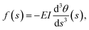 | (9) |
where θ is the angle between ds and dx as depicted inset of in the Fig. 21(g). As a result, the strain energy and lateral force could be obtained as depicted in Fig. 21(h) and (i). The static friction and interface shear strength are found to depend on the ultraviolet/ozone (UVO) treatment of PDMS. The shear strength starts at 0.30 MPa without UVO treatment, increases rapidly up to 10.57 MPa at 60 min of treatment and decreases for longer treatment, as shown in Fig. 21(j). Moreover, as observed from Fig. 21(k), water contact angle measurements suggest that the UVO-induced hydrophobic-to-hydrophilic conversion of PDMS surface is responsible for the increase in the static friction, while the hydrophobic recovery effect contributes to the decrease. The static friction between NWs and PDMS holds crucial importance in various applications of NWs, such as flexible/stretchable electronics, NW assembly, and nanocomposites (e.g., supercapacitors). The findings by Qin et al. provide valuable insights that can facilitate quantitative interface design and control for these applications. However, it is essential to acknowledge that the results are based on the assumption that contributions from axial stretching, and transversal shear are negligible. This assumption may introduce significant errors when calculating the friction force at the free ends of bent NWs. For instance, in the case of the NW illustrated in Fig. 21(g), the two free ends are expected to experience substantial static force, yet the obtained static forces at these locations are nearly zero.
 |
| | Fig. 21 (a–d) Optical micrographs of the initial to most bending states of a Si NW after extracted the W tip. (e and f) AFM images of the initial and final state of the Si NW. (g) AFM image of Si NW in the most-bent state, with the digitized data points and the geometric relationship (inset). (h and i) Strain energy and lateral friction force distribution along the NW as a function of s in (g). (j) Frictional shear strength between Si NWs and PDMS substrate at different UVO treatment times. (k) Dependence of frictional shear strength on the water contact angle. Reproduced with permission.174 Copyright 2011, ASC. | |
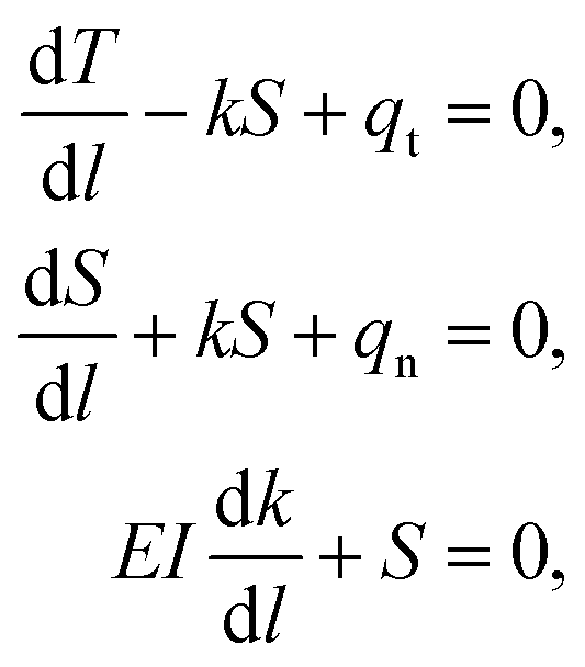
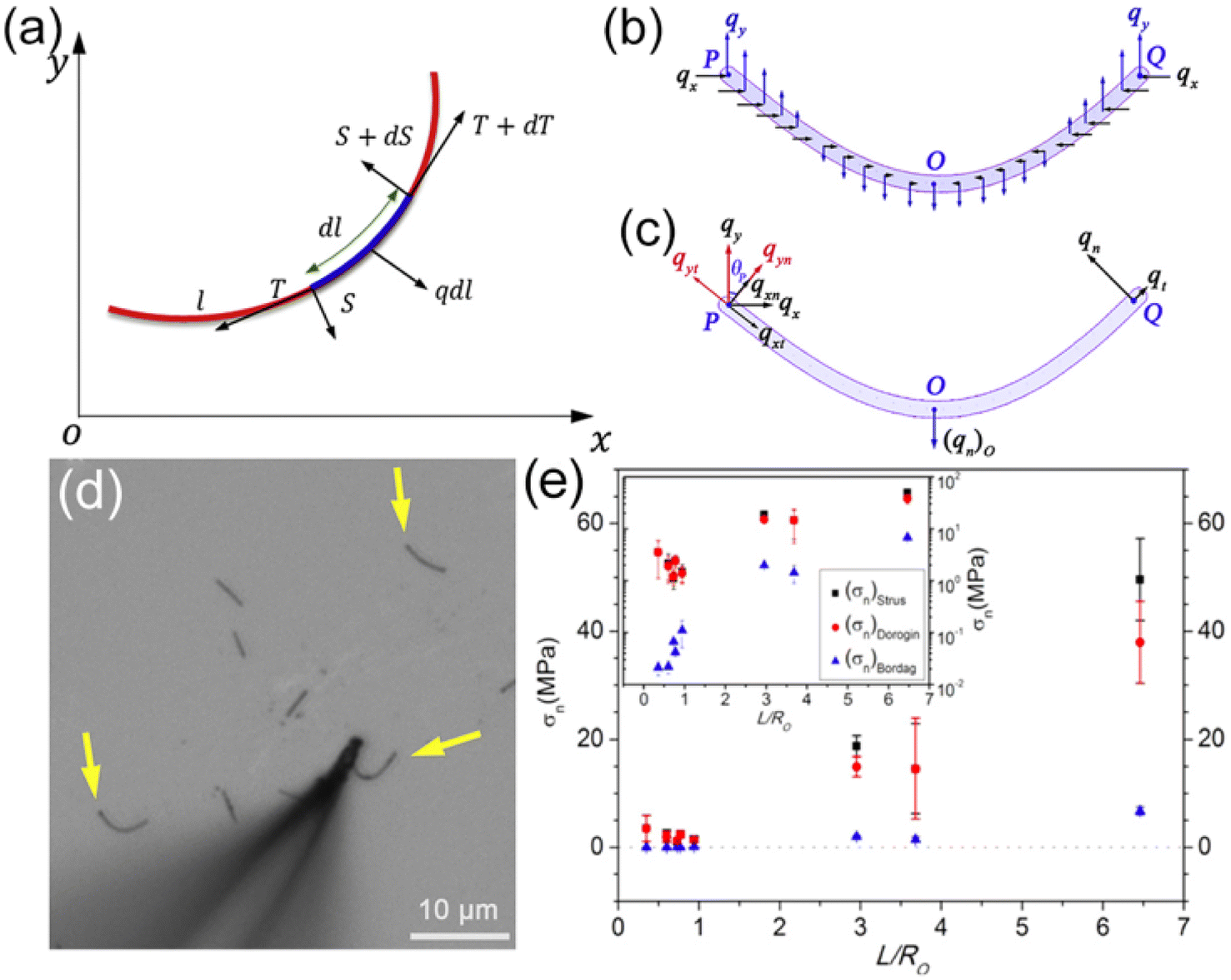
To further clarify the effects of transverse/tangential friction on the bending profile of NW in the most-bent method for calculating the static friction force between NWs and substrate, Hou et al. started the derivation from the force equilibrium equations for the bent NW depicted in Fig. 22(a)–(c),216
| |  | (10) |
where
T is the tension,
S is the shear stress,
l the coordinate along the natural axis of the NW,
qt and
qn are the normal and tangential components of the static friction per unit length acting on the NW, respectively.
T,
τk,
qt and
qn are the functions of
l. For a relatively short NW, a new expression was obtained,
| |  | (11) |
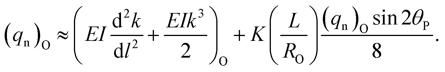
Here (
qn)
P and (
qn)
O are the normal friction forces at P and O, respectively,
L and
RO are the length of the NW and curvature radius at O, respectively, and
K = (
qn)
P/(
qn)
O. As the last term of
eqn (11) represents the contribution of the tangential friction force, it is suggested that the contribution of the tangential friction force to the bending of the NW is related to the value of
L/
RO. It is also shown that the second term is approximately equivalent to −(
qn)
O/10, and
eqn (11) can be approximately rewritten as,
216| |  | (12) |
where (
qn)
Dorogin was derived by Dorogin
et al. based on the assumption of
qt = 0.
195 If the NW profile is considered as a circular arc,
i.e. d
k/d
l = 0,
eqn (11) can be further simplified into the Bordag's equation, (
qn)
Bordag =
EIk3/2.
172 By assuming
T = 0 and
qt = 0,
eqn (11) can be also simplified Strus's equation, (
qn)
strus =
EId
2k/d
l2.
173 Finally, it is concluded that when
L/
RO ≤ 1, both the Dorogin's and Strus's models can achieve reasonable accuracy in estimating the static friction force, but the Bordag's equation will lead to a significant underestimation, as demonstrated in the experimental results shown in
Fig. 22(d) and (e). Based on
eqn (11), the average frictional shear stress between alumina (Al
2O
3) NWs and Si substrate are measured to be 2.41 MPa by the indirect OM-based measurement strategy.
216
 |
| | Fig. 22 (a) Schematics of the mechanical model for a bent NW segment held on a substrate by the static friction. (b and c) Distribution of the friction along x and y directions. (d) NWs manipulated to the most-bent state by the W tip under OM. (e) Frictional shear stress calculated by different mechanical models versus the L/RO value. The inset shows the corresponding values in the logarithmic coordinate. Reproduced with permission.216 Copyright 2015, IOP. | |
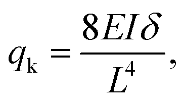
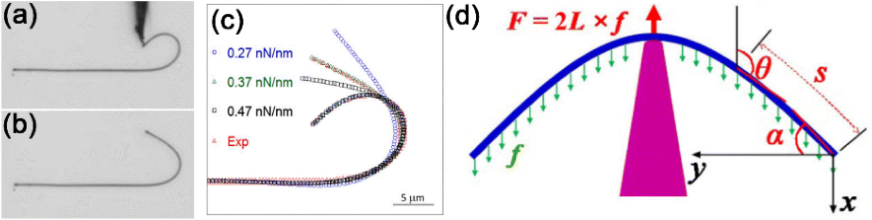
To further study the frictional behavior of 1D materials on substrate in air atmosphere, Wang et al. developed the push-to-slide method based on OM nanomanipulation.217 In their experiment, an initially straight NW was pushed at its midpoint using a W tip to slide at a constant speed along a substrate surface, as depicted in Fig. 23(a). The NW would bend into an arc shape due to the equilibrium between elastic force of NW and kinetic friction from the substrate. Assuming the deflection of the NW caused by NW-substrate friction is small and can be described by the small deflection beam theory, as illustrated in Fig. 23(b), the kinetic frictional force per unit length could then be derived from,217
| |  | (13) |
and the frictional shear stress could be further obtained by
σk =
qk/
w, where
w is the contact width between the NW and substrate.
Fig. 23(c) and (d) shows that the same NW on the same substrate, when pushed subsequently using two W tip with different shapes, exhibited the same bend shape, leading to the same frictional shear stress of about 2.0 MPa. This suggests the tip shape could not significantly affect the measured results. Meanwhile, it is should observed that the same NW, when pushed subsequently by the same W tip on Si and SiN substrates, exhibit quite different bent shapes, leading to different frictional shear stress of 2.0 and 1.5 MPa, respectively, as shown in
Fig. 23(d) and (e). These comparative test presented in
Fig. 23(f) directly demonstrated that the substrate could significantly affect the frictional force on NWs.
217 Similarly, Aditi
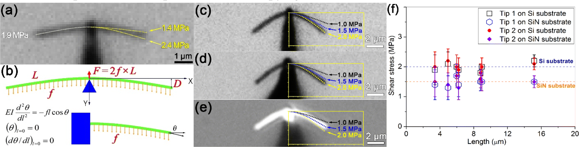
et al. further demonstrated that ZnO NWs on SiN and SiO
2 substrates exhibit different frictional shear stress values of 2.0 and 1.5 MPa, respectively, and the substrate effect on frictional shear stress was attributed to the differences in Hamaker constants and surface roughness of the substrates, as shown in
Fig. 24.
218
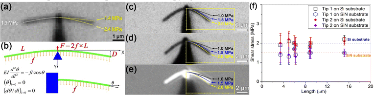 |
| | Fig. 23 (a) Optical micrograph of a NW, sliding on the Si substrate at a constant speed due to the push from a W tip. (b) Mechanical loading model for the sliding NW. (c and d) Optical micrographs of the same NW sliding on Si substrate pushed by tip 1 and tip 2, respectively. (e) The same NW to (c and d) slid on SiN substrate pushed by tip 2. (f) Frictional shear stress on Si and SiN substrates plotted as a function of the NW length. Reproduced with permission.217 Copyright 2015, AIP. | |
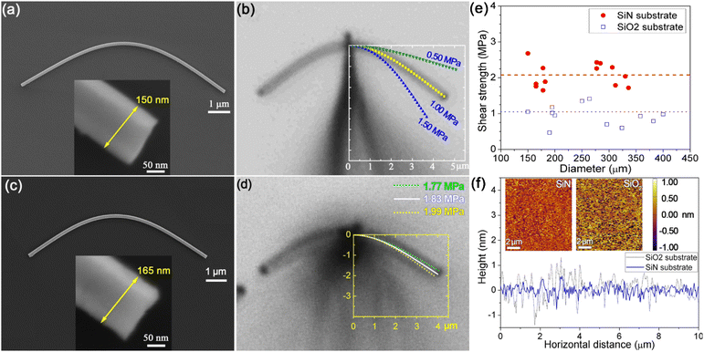 |
| | Fig. 24 Comparative test of ZnO NWs on SiN and SiO2 substrates: (a) SEM image of a ZnO NW on SiO2 substrate and (b) optical micrograph of the NW in (a) sliding on the substrate. The three dotted lines are the numerically modelled NW profiles using loads of 0.50, 1.00 and 1.50 MPa, respectively. (c) SEM image of a ZnO NW on SiN substrate. (d) Optical micrograph of the NW in (c) sliding on the substrate. The three curves represent the NW profiles simulated using loads of 1.77, 1.83 and 1.99 MPa, respectively. (e) The kinetic frictional shear stresses of ZnO NWs on SiN and SiO2 substrates plotted as a function of the NW diameter. (f) AFM images of the SiN and SiO2 substrate surfaces and their corresponding cross-sectional line profiles. Reproduced with permission.218 Copyright 2016, Elsevier. | |
The assumption of small deflection significantly limited the use of eqn (13) in many actual tests, where the NW being tested usually have length over 10 µm. In 2016, Xie et al. proposed a simple analytical formula calculate the kinetic friction per unit length (fk) on the bent NWs with relatively large deformation based on the force-equilibrium model,219
| | 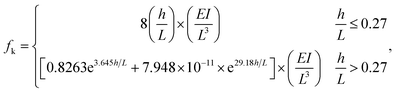 | (14) |
where
h and
L are the deflection of the NW end and the half-length of the NW. As evident from the results presented in
Fig. 25(a)–(e),
eqn (14) exhibited a high level of reliability in estimating the kinetic frictional force on NWs with various lengths and deflections.
219 Moreover, as can be seen from
Fig. 25(c) and (d), for the relatively long NW, bending shapes for the sliding state and the static shape after tip removal are different, and the difference in their bending energies, Δ
U =
Ui −
Uf, could be derived from their shapes as shown in
Fig. 25(f).
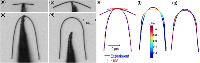 |
| | Fig. 25 (a–c) Optical micrographs of three NW segments with difference lengths pushed to slide along the Si substrate by a W tip. (d) Optical micrograph of the NW shown in (c) after tip removal. (e) The comparison of NW profiles before tip removal from the tests and the FEM simulations. (f) Distribution of elastic energies per unit length of the bent NW shown in (c) and (d), and (g) the corresponding the swept area Aswept (crossed). Reproduced with permission.219 Copyright 2016, IOP. | |
From the perspective of energy-conversion, the work Wf done by the friction should be equal to the reduction of the bending energy, ΔU, restored in the NW during the bouncing process form Fig. 25(c) and (d). As Wf could be estimated by the swept area, Aswept, for NW scanning from initial bending state to final bending state, using Wf = −fkAswept, the kinetic friction fk could be obtained by,219
| | | fk = (Ui − Ufinal)/Aswept. | (15) |
In their test, 16 SiC NWs with different diameters and lengths on SiN substrate were examined. As shown in Fig. 25, the frictional shear stress was determined to be ranged from 0.18 to 0.51 MPa, and from 0.21 to 0.62 MPa by using the force equilibrium and energy conservation models, respectively.219 Clearly, the frictional shear stress values determined from the two methods are quite close. Besides the calculation based on the swept area shown in Fig. 25, Xie et al. also proposed a method presented in the Fig. 26(a)–(c), where the swept area of NW end is much easy to identified.142
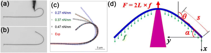 |
| | Fig. 26 (a–c) Initial bending status and final bending status of a NW on substrate after the tip withdrawal, and the simulated final bending statuses at different friction forces compared to the experimental, respectively. Reproduced with permission.142 Copyright 2015, Springer Nature. (d) The cantilever model for a NW sliding in a stable manner on a substrate at a constant speed. Reproduced with permission.139 Copyright 2022, Springer Nature. | |
The approximate analytical expression for force-equilibrium method introduced by Xie et al. allows the calculation of friction force through a direct algebraic expression, where the dimensionless shape factor, h/L, can be conveniently measured by OM. This is simpler and demands less image processing techniques, compared to the previous methods where calculating friction force required iterative adjustments through best-fitting the numerically computed bent profile. Recently, a more precise analytical expression for force-equilibrium method, based on the non-linear elastic beam model shown in Fig. 26(d), has been employed for calculating the kinetic friction force between ZnO NWs and graphite surface,139
| |  | (16) |
3.3.2.2. Frictional behavior between NWs.
The friction forces between individual NWs could also be determined the direct OM-based measurement strategy, which was first achieved by Wang's group in 2018. As shown in Fig. 27, Two NWs were individually fastened at the edges of two Si substrates to form two NW cantilevers, and the suspended segments were cross overlapped. One Si substrate could be laterally moved, while the other substrate was fixed, resulting in the shearing of the crossly overlapped point between the two NWs. As the testing process was visualized under the OM, the shearing process between the two NW could be directly identified from the deflection of the target NW. As an example, Fig. 27(c)–(g) depicted the initial status, intermediate status, status prior to relative sliding between the two NWs, occurrence relative sliding, and right after bouncing backward in the opposite direction to the movement of the manipulator NW. In principle, the friction between the two NWs could be derived from the deflection of the target NW. However, in actual tests, it is quite difficult to adjust the relative position between the two NWs.
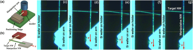 |
| | Fig. 27 (a and b) Sketches for OM-nanomanipulation system and positioning of NWs for friction testing, respectively. (c–g) Optical snapshots of a target NW being deflected by a manipulator NW during friction testing. Reproduced with permission.220 Copyright 2018, IOP. | |
Recently, Yibibulla et al. developed a simpler setup for testing the frictional force between two crossly overlapped NWs. In their experiment, two individual SiC NWs were cantilevered at the adjacent edges of a TEM grid by vdW force, forming a crossed cantilevers, as depicted in Fig. 28(a)–(e). As the manipulator m-NW and target t-NW were positioned at the same substrate, it is much easier to observe the deflection of t-NW during the shearing process, as compared to the test system developed by Xie et al.220 According to the small-deflection beam model shown in Fig. 28(f), the static friction force between the two NWs could be calculated by,221
| |  | (17) |
where,
δy is the maximum displacement distance of contact point of the NWs along with the
y direction. Moreover, assuming that the released elastic energy of t-NW during the sliding back equals to the kinetic friction energy between NWs, the kinetic friction force between the two NWs could then be derived from,
221where
δM is the
y direction maximum displacements of contact points at each most bending state, and
δN is the
y direction distance between the initial position of the contact point of NWs and the point where it rebounds and slips back. As can be observed in
Fig. 29(a)–(h), the two NWs consistently remain in the same plane during the shearing process, and sliding process is actually composed of numerous discontinuous stick-slip events. As the sizes and morphologies of the two NW could be identified by SEM after the test (see
Fig. 29(i)–(m)), the average kinetic shear stress corresponding to the whole shearing process was measured to be
τk = 6.4 ± 1.1 MPa, and the maximum static shear stress was
τs = 7.8 ± 1.6 MPa. These values are much greater than the values of 0.7–1.3 MPa and 0.4 to 0.8 MPa for the static and kinetic shear stresses between Al
2O
3 NWs, respectively.
220 Additionally, these values surpass the value of 1–3 MPa commonly found in most NW-substrate interfacial systems.
 |
| | Fig. 28 (a) Physical photograph for the OM-nanomanipulation system. (b) Top-view SEM image of a Si TEM grid. (c) Cross-section of the grid's window edge (Side-view image). (d) Optical micrograph showing two SiC NWs on a Si TEM grid during shearing. (e) 3D model showing the geometry of the contact area between the two SiC NWs. (f and g) Schematic illustration of the mechanical models for the calculation of static and kinetic frictional forces between two individual NWs, respectively. Reproduced with permission.221 Copyright 2022, Wiley. | |
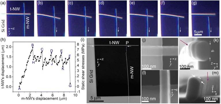 |
| | Fig. 29 (a–g) High-magnification OM images (x–y plane view) of t-NW being deflected by m-NW during shearing at different stages. (h) Stick-slip curve obtained by plotting displacements at the contact point of the t-NW and m-NW as a function of the displacement of the m-NW. (i) Low-magnification x–y plane-view SEM image of (g) state. (j and l) The high-magnification x–y plane view SEM images of the lateral profiles of t and m-NWs. (k and m) The high-magnification SEM images of cross-sectional profiles of t and m-NWs. Reproduced with permission.221 Copyright 2022, Wiley. | |
3.3.3. Achievements and challenges in OM-based measurement strategies.
From the early stages of OM-based direct measurement strategies to the sophisticated manipulation-based methodologies, the trajectory of OM techniques has undergone a profound evolution. This evolution is notably characterized by substantial advancements in understanding the interfacial frictional behavior, progressing from the interaction of 1D materials with substrates to the intricate frictional behavior between individual 1D materials. OM-based strategies offer a cost-effective, convenient, and visually intuitive approach, particularly well-suited for real-time monitoring of the frictional behavior of 1D materials, such as interactions between NWs and substrates or among individual NWs. The visualizable manipulation mode can significantly enhance the testing efficiency compared to AFM-based strategies, especially when testing friction forces between individual 1D materials where the complex contact relationships between NWs and AFM tips are challenging to distinguish. Additionally, OM-based strategies are adaptable to diverse environmental conditions, including humidity and temperature, and hold the potential to investigate the contribution of electrostatic forces to the frictional behavior of 1D materials. However, the limitation in spatial resolution of OM can significantly impede or restrict applications in certain frictional behaviors of 1D materials, such as stick-slip behavior and vibrational characteristics at the atomic scale. Future integration of laser Doppler techniques holds the potential to enhance OM-based strategies, addressing the spatial resolution limitations and expanding their applications in nanomechanical testing of 1D materials. This advancement could also broaden their applications in the scope of nanomechanical characterizations. The experimental results obtained through OM techniques so far are summarized in Table 3.
Table 3 List of experimentally determined frictional properties of 1D materials with substrates and between two individual 1D materials measured by OM-based techniquesa
| Techniques |
Interfaces |
Friction parameters |
Notes |
Ref |
|
w
f: Friction energy, w: width, h: height, NG-natural graphite SiO2, HOPG-highly oriented pyrolytic graphite, UVO: ultraviolet ozone.
|
| Micromechanical tester |
SWCNT–SWCNT |
w
f = 0.22 N m−1 |
D = 40 nm; A = 6.05 × 10⁷ nm2 |
225
|
| OM-sensor |
ZnO NW-Si substrate |
µ
k = 25–45; σk = 1 MPa |
Hexagonal R = 100 nm; L = 30–40 µm; ambient |
125
|
| OM-sensor |
Pt NW-W tip |
µ
s = 0.23 ± 0.02; µs = 0.2 ± 0.01; σk = 1 MPa |
Circular; D = 625 nm; atmosphere |
223
|
| OM- sensor |
Pan fiber-Pan fiber |
Several tens MPa |
Circular, D = 400–4000 nm; T ≈ 23 °C; RH ≈ 20–50% |
224
|
| OM-manipulation |
Si NW-PDMS |
σ
maxs = 0.3 MPa; qmaxs = 0.006 nN nm−1 |
Hexagonal; D = 35–55 nm; L = 4–8 µm; T ≈ 23 °C; RH ≈ 50% |
174
|
| OM-manipulation |
Si NW-PDMS |
σ
maxs = 10.57 MPa; qmaxs = 0.236 nN nm−1 |
Hexagonal; D ≈ 35–55 nm; L ≈ 4–8 µm; T ≈ 23 °C; RH ≈ 50%; 60 min UVO treatment |
174
|
| OM-manipulation |
Al2O3 NW-Si substrate |
σ
s = 0.68–2.7 MPa; σk = 1.16–3.4 MPa |
Rectangular; w = 69–290 nm; h = 87–487 nm; T ≈ 25 °C; RH ≈ 35% |
142
|
| OM-manipulation |
Al2O3 NW-Si substrate |
q
s = 0.32 nN nm; σs = 2.41 MPa |
Rectangular; w = 86 nm; h = 135 nm; L = 3.38–9.05 µm; T ≈ 25 °C; RH ≈ 35% |
216
|
| OM-manipulation |
Al2O3 NW-Si and SiN substrate |
σ
s (on Si) = 2.06 ± 0.2 Mpa; σk (on SiN) = 1.5 ± 0.2 MPa |
Rectangular; w = 133 nm; h = 86 nm; L = 3.6–8.3 µm; T ≈ 25 °C; RH ≈ 35% |
217
|
| OM-manipulation |
ZnO NW-amorphous SiO2; ZnO NW- SiN substrate |
σ
k (on SiO2) = 1.05 ± 0.28 MPa; σk (on SiN) = 2.08 ± 0.33 MPa |
D = 150–400 nm; T ≈ 25 °C; RH ≈ 35% |
218
|
| OM-manipulation |
SiC NW-SiN substrate |
σ
k = 0.18–0.51 MPa (force-equilibrium model); and σk = 0.21–0.62 MPa (energy-conservation model) |
D = 50–370 nm; L = 5–41 µm; T ≈ 25 °C; RH ≈ 35% |
219
|
| OM-manipulation |
Al2O3 NW-Si substrate |
— |
L = 3.1–32.35 µm; T ≈ 25 °C; RH ≈ 45% |
126
|
| OM-manipulation |
SiC NW-SiN substrate |
σ
k = 127–166 MPa |
A = 945–11![[thin space (1/6-em)]](https://www.rsc.org/images/entities/char_2009.gif) 441 nm2; T ≈ 25 ± 5 °C; RH ≈ 45 ± 15% 441 nm2; T ≈ 25 ± 5 °C; RH ≈ 45 ± 15% |
222
|
| OM-manipulation |
Al2O3 NW-Al2O3 NW |
σ
s = 0.71–1.34 Mpa; σk = 0.43–0.82 Mpa |
— |
220
|
| OM-manipulation |
SiC NW-SiC NW |
σ
s = 7.1 ± 0.8 MPa; σk = 14.7 ± 1.8 MPa; σs = 5.2 ± 1.1 MPa; σk = 64.4 ± 7.2Mpa; σs = 18.7 ± 3 MPa; σk = 49.6 ± 5.8 MPa |
Hexagonal; D1 = 96–324 nm; D2 = 58–186 nm; A = 8.41 × 10²–1.12 × 10⁴; RT; RH ≈ 20–40%; 40–60%; 60–74% |
221
|
| OM-manipulation |
ZnO NW-NG; ZnO NW-HOPG |
σ
s (on NG) = 0.48 MPa; σs (on HOPG) = 0.25–2.785 MPa |
Hexagonal; D = 485–142 nm; T ≈ 25 °C; RH ≈ 50% |
139
|
4. The influencing factors for the frictional behavior of 1D materials
4.1. Material combinations
It is widely recognized that the materials in contact play a pivotal role in determining friction behavior, with their varying surface energies, atomic structures, and adhesion properties contributing to distinct friction responses. Thanks to advancements in AFM measurements and molecular dynamics simulations, our understanding of interfacial material combinations influencing frictional behavior at the atomic scale has significantly improved. It is generally expected that material combinations also exert a substantial impact on the frictional behavior of 1D materials. However, due to challenges in characterization, there are limited reported results on this topic, and the fundamental understanding remains largely unclear.
In 2010, Conache et al. comparatively measured the frictional shear stress of InAs NWs on three distinct substrates, SiO2, fluorosilanized SiO2, and silicon nitride (Si3N4), using the indirect AFM-based measurement strategy.177 It was shown that on all three substrates thick NWs showed a difference between sliding and static friction of up to three orders of magnitude – a behavior that is usually associated with atomic-scale point contacts. Moreover, all three substrates exhibit quite similar static frictional behavior, suggesting that the condensed water layer that must be present on the oxide and nitride surfaces does not significantly affect the friction of NW. Subsequently, Wang et al. comparatively tested the friction forces of different NWs on various substrates using the OM-based measurement strategy.217,218 It was found that the frictional shear stress of Al2O3 NWs on Si and SiN substrates was 2.0 ± 0.2 and 1.5 ± 0.2 MPa, respectively,217 while the frictional shear stress for ZnO NWs on SiO2 and SiN substrates was 1.05 ± 0.28 and 2.08 ± 0.33 MPa, respectively.218 Kim et al. tested the friction of oxidized Si NWs on thermally grown SiO2 and CVD-deposited single-layer graphene using the direct AFM-based strategy.180 The frictional shear stress between the oxidized Si NWs and the SiO2 substrate was estimated to be ranged from 7.5 to 12.3 MPa, while that between the oxidized Si NWs and the graphene substrate ranged from 4.7 to 7.0 MPa.180 In addition, the result also suggested that the dependence of shear stress on the radius of the NWs was not significant, which is quite consistent with the frictional behavior of ZnO and Al2O3 NWs on Si, SiO2 and SiN substrates obtained by Wang et al.,217,218 but quite different from those observed for InAs NWs on SiO2, fluorosilanized SiO2, and Si3N4 substrates by Conache et al.177 Although these comparatively measurements demonstrated that different substrates or 1D materials could significantly affect the frictional behavior of 1D material, it is still quite hard to isolate the contribution of material combinations on the interfacial friction. This is because the different NWs or substrates used in the test many have different roughness, while the interfacial friction is quite sensitive to the roughness. To isolate the contribution of material combination, Hou et al. comparatively measured the frictional shear stress of the CVD-grown hexagonal ZnO NWs on natural graphite and mica substrates.139 Both substrates have similar surface roughness values of subangstrom-scale and interfacial adhesion energies with ZnO NWs. Yet, a kinetic frictional shear stress of 0.51 MPa was obtained for the ZnO-graphite system, significantly lower than that of 5.1 MPa for the ZnO-mica system, as depicted in Fig. 30. The results demonstrate that the kinetic friction at a perfectly smooth contact interface may not be controlled by the adhesion, whilst being commonly referred to as adhesive friction or adhesion-dominated fiction.
 |
| | Fig. 30 (a) Optical image of a ZnO NW sliding stably on the graphite substrate. (b) SEM image of the ZnO NW in (a) after the test. The inset in (b) shows the hexagonal structure of the NW. (c) The kinetic shear stresses of ZnO NWs on graphite substrate plotted as a function of the diameter of NWs. (d) Optical image of a ZnO NW sliding stably on the mica substrate. The SEM image inset in (d) shows the hexagonal structure and diameter of the ZnO NW. (e) The kinetic shear stresses of ZnO NWs on mica substrate plotted as a function of the diameter of NWs. Reproduced with permission.139 Copyright 2022, Springer Nature. | |
4.2. Surface roughness
Numerous friction tests on 1D materials conducted on smooth substrates consistently reveal a proportional relationship between the friction force of 1D materials and substrates and their respective contact areas. This observed correlation aligns with the behavior noted in AFM tips and nanoparticles on smooth substrates.113,226 However, when 1D materials are placed on rough substrates, a more intricate friction behavior emerges. In such cases, 1D materials may span regions of the substrate containing surface features, influenced by mechanical constraints imposed by contact with surface steps, asperities, or wavinesses. This bridging phenomenon may lead to a substantial reduction in the real contact area. Consequently, the friction force, directly proportional to the real contact area, decreases on substrates with uneven surface topography.126,139,196,222 Conversely, 1D materials may conform to the topography of a substrate, resulting in a notable increase in friction compared to its bulk counterpart. This increase is widely accepted as the primary contributor to the elevated friction/adhesion observed in gecko-like fiber-based adhesives.99,227,228 On the other hand, when sliding over a rough substrate, 1D materials may experience increased frictional forces due to mechanical interlocking and the presence of a Schwoebel barrier at steps or asperities, similar to observations when AFM tips and nanoparticles slide over a rough substrate.229,230 However, despite theoretical considerations regarding the size/diameter-dependent frictional behavior of 1D materials, experimental validation of this dependency remains challenging due to substantial experimental challenges associated with their testing.
Polyakov et al. firstly conducted a study on the effect of surface roughness of the substrate on the static frictional properties of 1D materials. In their comparatively test, the static friction forces of 5.8, 3.9, 1.4, and 0.6 nN nm−1 were obtained for copper oxide (CuO) NWs on amorphous silicon substrates with different roughness of 0.7, 2.1, 5.4, and 16.1 nm, respectively.196 Moreover, they analyzed the approximately an order of magnitude decreases in friction force using the real contact area, which was found through a multiple elastic asperity model based on the Derjaguin–Muller–Toporov contact mechanics. In the subsequent study by Xie et al.,222 the frictional shear stress on SiC NWs was found may decrease from 0.38 to 0.02 MPa for the SiN substrates with increased roughness from 0.5 to 23 nm. Moreover, it was suggested that there is a power-law relationship between frictional stress and surface roughness as shown in Fig. 31(a), and the substrate's effect was primarily driven by changes in the number of contact asperities between a NW and a substrate according to the Monte Carlo calculations.
 |
| | Fig. 31 (a) Frictional shear stress of SiC NWs against the surface roughness of SiN substrate. Reproduced with permission.222 Copyright 2017, Springer Nature. (b) Dependences of frictional shear stress of ZnO NWs on HOPG and NG substrates on the NW diameter. (c) Sketches of a NW conforming to a wavy substrate surface and the step-induced gap between the NW and substrate surface. Reproduced with permission.139 Copyright 2022, Springer Nature. | |
The effect of substrate surface texture on the friction of the 1D materials was firstly investigated by Xie et al., by the comparative test of Al2O3 NWs on Si substrates, which were grooved to have different textures using nanoscratching performed on a HYSITRON Triboindenter®.126 It was found that Al2O3 NW could span across relatively narrow grooves, but might be in contact with the bottom of relatively broad grooves, dependent on the adhesion energy and elastic compliance of the NW. In particular, for the narrow grooves, they proposed a quantitative criterion based on the classic theory of elasticity to predict the contact status between a NW and a grooved surface. Assuming that the cross-sectional profile of the narrow grooves is sinusoidal, the criterion can be written as,126
| | | tc = [12γwg4/(π4Ehg2sin4φ)]1/3 | (19) |
where
tc is the critical thickness of the NW,
γ is interface energy for the NW/substrate system,
φ is the angle between a tangent on the longitudinal axis of the bent NW and the groove direction,
E is the elastic modulus of the NW, and
wg and
hg are the height and width of the groove, respectively. For a NW with a thickness of
t, if
t >
tc, the NW will span over the groove, and if
t <
tc, the NW will be in contact with the bottom of the grooves. Moreover, a genetic algorithm was developed to determine the effective contact area between the NW and the textured substrate. The frictional force was found to be nearly proportional to the effective contact area, regardless of width, depth, spacing and orientation of the surface textures. It is interesting to found that interlocking caused by textured grooves was not observed in this study.
To further identify the effects of surface waviness and step, Hou et al. recently comparatively test the friction behavior of ZnO NWs on natural graphite (NG) and highly oriented pyrolytic graphite (HOPG) substrates in ambient conditions.139 NWs on the step-free and waviness-free NG substrate exhibit a diameter-independent nominal frictional shear stress of 0.48 MPa, and this provides a benchmark for studying how the surface topography of graphite influences NW friction. NWs on the HOPG substrate present a significant diameter-dependent frictional shear stress, increasing from 0.25 to 2.78 MPa with the decrease of NW diameter from 485 to 142 nm, as shown in Fig. 31(b). The waviness of HOPG has a limited effect on the NW friction, as a NW can fully conform to the substrate. However, unlike the Al2O3 NWs on grooved Si substrates,126 the surface steps on the HOPG can significantly enhance the NW friction and lead to a much higher frictional shear stress than that on NG due to mechanical blocking and the presence of a Schwoebel barrier at step edges. The surface steps, however, can also generate small wedge-shaped gaps between a NW and substrate, and thus reduce the NW friction, as shown in Fig. 31(c). With the decrease in NW diameter, the capacity for the NW to better conform reduces the length of the wedge-shaped gaps, leading to the observed increase in NW friction.
4.3. Relative humidity
The frictional behavior of nano-objects on substrates can be significantly affected by humidity or moisture in the environment. This aspect has been extensively studied over the past several decades, primarily through the measurement of friction between AFM tips and substrates or between nanoparticles and substrates using AFM.231–234 Previous findings suggest that absorbed water molecules may serve as lubricants, reducing interfacial friction, but they can also contribute to the formation of a liquid bridge at the interface, thereby increasing interfacial friction. However, the impact of environmental humidity on the frictional behavior of 1D materials remains largely unclear, mainly due to the substantial challenges faced in actual experimental characterization.
The initial quantitative exploration of the impact of relative humidity (RH) on the interfacial frictional behavior of individual NWs was carried out by Yibibulla et al.221 The investigation involved testing the frictional behavior between NW contact pairs in air, as illustrated in Fig. 29. In their experiment, the frictional forces between NW contact pairs were assessed under environmental RH ranging from 20% to 74%. As shown in Fig. 32(a), the average static and kinetic shear strengths, τs = 7.1 ± 0.8 MPa and τk = 5.2 ± 1.1 MPa, are found to be insensitive to the RH within the range of 40–60%, and obvious slick-stick behavior was observed during the sliding process (see Fig. 29(h)). When the RH increased to 74%, the shear strength values increase to τs = 18.7 ± 3.0 MPa and τk = 14.7 ± 1.8 MPa. Conversely, with a decrease in RH to 20%, a significant surge in both static and kinetic shear strengths is observed: τs = 64.4 ± 7.2 MPa and τk = 49.6 ± 5.8 MPa. Furthermore, the sliding process between two individual SiC NWs displays pronounced irregular stick-slip behavior in a relatively low RH environment (below 30%, see Fig. 32(c)). However, the stick-slip behavior becomes much smoother with increasing RH, as depicted in Fig. 32(b). The effects of humidity on the shearing behavior between two intersected NWs could be understood as follows (see the schematic diagrams shown in Fig. 32(d)–(f)). The heightened frictional shear stress at relatively low RH was ascribed to the mechanical interlocking of surface defects and asperities present on the NWs. In conditions of moderate RH, ranging from 40% to 60%, an absorbed water layer on the NW surfaces served as a lubricant between the sliding surfaces, resulting in a reduced shear strength. With an RH above 60%, the formation of a water meniscus at the contact area introduced viscous damping during sliding, consequently increasing the shear strength. This damping effect could also attenuate stick-slip behavior. At the conclusion of the shearing process of a NW pair in a high RH environment, an ultimate shear strength of several tens of MPa was achieved, indicating that the complete detachment of the NWs was associated with the rupture of a meniscus bridge.
 |
| | Fig. 32 (a) The average static and kinetic frictional shear strengths of all tested NW pairs plotted as a function of environmental RH. (b and c) Characteristic deflection/shear stress progression of selected NW pairs obtained at 74% and 29% RH, respectively. (d–f) Schematic diagrams to show the effects of humidity on the shearing behavior between two intersected NWs. The blue mesh in (d–f) illustrates the presence of a water film and meniscus. Reproduced with permission.221 Copyright 2022, Wiley. | |
The observed humidity effect on the frictional behavior between NWs, as directly investigated by Yibibulla et al.,221 is believed to contribute to the advancement of novel approaches for dispersing and manipulating 1D materials. Additionally, it holds potential for optimizing the design of new devices based on arrays of 1D materials. However, it is crucial to highlight that the fundamental mechanisms concerning the impact of humidity on the frictional behavior of 1D materials remain elusive. This is due to the limited experimental results obtained thus far, emphasizing the need for thorough experimental measurements, theoretical calculations, and simulations for further exploration.
4.4. Non-uniformity, heterogeneity, surface modification, and anisotropy
The frictional behavior of non-uniform and heterogeneous 1D materials is an intriguing yet complex research direction in the field of nanotribology. A 1D nanomaterial can be geometrical non-uniform, due to variation in the shape or size of its cross-section along its longitudinal axis. The surface of a 1D nanomaterial can also be heterogeneous due to the presence of defects, contamination, or through surface modification. The composition of 1D material may also be heterogeneous due to, for example, a composition gradient or stepwise change in composition along its longitudinal axis, or due to the addition of a coating, through surface modification, or the presence of core–shell structure. 1D nanomaterials. 1D nanomaterials that exhibit irregularity or heterogeneity with respect to their longitudinal will, by nature, have the tendency to exhibit anisotropic frictional behavior. This can be simply explained by recognizing that the compositional or geometric condition of the interface between the 1D material and a surface it comes into contact with will differ along its length. Therefore, when a frictional force is applied to a 1D material in a different direction or location, a different interface location, with a different compositional and geometric condition, may take part in the friction interaction, and therefore provide a different friction response. If the complex friction behavior of irregular and heterogeneous 1D materials can be understood, then the careful design of a 1D material's geometry and composition could be used to provide tailored and anisotropic friction behavior to suit a particular application. Additionally modifying the surface of non-uniform 1D nanomaterials through functionalization or a coating can be carried out in order to tailor the material's frictional performance.235–238 For example, recently Wu et al. fabricated a snake-inspired smart nano-stepped surface by replicating the microfibril structure of the ventral scales of the Chinese cobra into a thermo-responsive shape-memory polymer. During heating, this surface transitions from a flat structure to one with nano-steps, imparting frictional anisotropy. The desired frictional anisotropy can be tailored by halting the heating process. Utilizing this surface, they achieved unidirectional transport of particles and demonstrated dry self-cleaning.141
Only a small number of studies have made experimental progresses in investigating the anisotropic nature of friction in 1D materials. For example, in 2009, Lucas et al. firstly observed anisotropy in the shear strength of CNTs in the transverse and longitudinal direction by AFM, as illustrated in Fig. 9.137 This was explained through molecular dynamics simulations, where friction in the vertical direction induced a soft “hindered rolling” of the nanotube and frictional dissipation, which was absent or partially absent when the tip slid parallel to the CNT axis, especially for chiral CNTs. While their findings provide initial experimental insights into the anisotropy of friction in 1D materials, these experimental findings fall short in adequately addressing the complexities of frictional behavior in non-uniform 1D materials.
To date, the understanding of the frictional behavior of 1D materials obtained through experimental studies, whether involving friction between 1D materials and substrates or between 1D materials themselves, has assumed a uniform and smooth surface for 1D materials. In reality, 1D materials may not be uniform; surface roughness, defects, and unevenly distributed cross-sections can influence the actual contact area and alter the frictional response during sliding. Nevertheless, previous studies either focused on substrate roughness or attributed errors to factors such as surface defects in 1D materials, without quantifying the impact of defects in 1D materials on frictional behavior. For instance, in a recent friction experiment between two individual SiC NWs, Yibibulla et al. observed an uneven surface of SiC NWs,221 as indicated by the red arrows in Fig. 29(m) and (k). However, they did not quantify the irregularity of the NW's surface and its impact on their frictional behavior; they merely briefly mentioned the effect of uneven surfaces on frictional results.
5. Outlook
This review thoroughly outlines the experimental measurement methods employed to assess the frictional behavior of 1D materials, which include AFM, SEM, and OM-based measurements. Through a comprehensive evaluation of these methods, the paper delves into their strengths and limitations in the actual testing process, shedding light on the challenges associated with characterizing the friction behavior of 1D materials. Apparently, AFM and SEM-based measurements have proven highly feasible in studying the static, kinetic, and rolling friction of 1D materials, yielding valuable results in the initial study on the frictional behavior of 1D materials. This success can be attributed to the well-developed and commercialized AFM and SEM testing systems with high space and force resolutions. However, AFM-based measurements face challenges such as low testing efficiency and considerable uncertainty in the complicated contact relationships between the AFM tip, 1D material, and substrate during practical tests due to the lack of real-time direct visual feedback. Meanwhile, SEM-based measurements operate in a high vacuum with high-energy electron beam irradiation, lacking the capability to assess the effects of environmental humidity and facing challenges in eliminating possible charging effects from the electron beam irradiation. On the other hand, OM-based measurements have demonstrated greater proficiency and cost-effectiveness in measuring the frictional behavior of 1D materials, thanks to the ease of operation and low cost of OM-based testing systems. Furthermore, similar to AFM-based measurements, OM-based measurements enable testing processes in various environmental conditions, and thus are expected to serve as a powerful and effective route for testing the environmental parameters on the frictional behavior of 1D materials. However, the relatively limited space resolution of OM may hinder the testing of ultra-small 1D materials and the frictional behavior at the atomic scale.
Building on these advancements, current research has primarily focused on studying the frictional behavior of a limited set of 1D materials and substrates with smooth contact surfaces. While these studies provide valuable insights, there is a notable gap that calls for a more extensive exploration of various interfacial material combinations and surface topographies (roughness) to comprehensively capture and understand the frictional behavior of 1D materials. Additionally, accurately determining the contact area between 1D materials and substrates or between individual 1D materials plays a key role in understanding frictional behavior but remains a challenge across all currently available measurement techniques. To address this limitation, enhancements in imaging techniques, such as higher resolution microscopy and advanced manipulation tools, are essential. Furthermore, the influence of the non-uniformity, testing environment and sliding velocity on the friction behavior of 1D materials stands out as the critical factors in the design of 1D materials-based devices for real-word applications. Research into the impact of non-uniformity, environmental factors (temperature, humidity, and atmospheric conditions) and sliding velocity is necessary for a comprehensive and in-depth understanding in future.
The frictional behavior between individual 1D materials is crucial for enhancing gecko-inspired materials and optimizing reversible adhesives. Despite significant advancements in synthesis, the clumping between adjacent 1D materials due to strong surface forces remains a persistent issue. Tackling this challenge requires a comprehensive understanding of the frictional and adhesive behaviors between individual 1D materials and the underlying mechanisms. Unfortunately, research in this specific context is still in its early stages. While there has been notable progress in investigating the sliding and peeling behaviors of 1D materials from substrates, the nuanced study of detachment between two or more individual 1D materials remains in a preliminary phase. Preliminary findings indicate that the combined impact of environmental humidity and sliding velocity can notably affect the frictional behavior of 1D materials, particularly the friction forces between individual 1D materials. It is anticipated that OM-based measurements, offering visualizable manipulation under ambient atmosphere conditions, will play a key role in elucidating this specific topic.
Conflicts of interest
The authors declare that there is no conflict of interest.
Acknowledgements
This project was financially supported by the National Natural Science Foundation of China (No. 12072111 and 11674399).
References
- S. Wang, L. Ma, J. L. Mead, S.-P. Ju, G. Li and H. Huang, Sci. China: Phys., Mech. Astron., 2021, 64, 254612 CAS.
- T. Yibibulla, Y. Jiang, S. Wang and H. Huang, Appl. Phys. Lett., 2021, 118, 043103 CrossRef CAS.
- L. Ma, Y. Jiang, G. Dai, J. L. Mead, T. Yibibulla, M. Lu, H. Huang, S. Fatikow and S. Wang, J. Phys. D: Appl. Phys., 2022, 55, 364001 CrossRef CAS.
- L. Hou, Y. Gao, T. Yibibulla, H. Huang and S. Wang, Phys. Status Solidi - Rapid Res. Lett., 2022, 16, 2200039 CrossRef CAS.
- L. Ma, T. Yibibulla, Y. Jiang, J. L. Mead, M. Lu, S. Wang and H. Huang, Phys. E, 2022, 136, 114990 CrossRef CAS.
- Y. Jiang, M. Lu, S. Wang and H. Huang, Mod. Phys. Lett. B, 2021, 35, 2150350 CrossRef CAS.
- H. J. Joyce, J. L. Boland, C. L. Davies, S. A. Baig and M. B. Johnston, Semicond. Sci. Technol., 2016, 31, 103003 CrossRef.
- J. Hu, M. Ouyang, P. Yang and C. M. Lieber, Nature, 1999, 399, 48–51 CrossRef CAS.
- V. Schmidt, J. Wittemann and U. Gosele, Chem. Rev., 2010, 110, 361–388 CrossRef CAS PubMed.
- X. Zhen, L. Hou, Y. Gao, M. Hou and S. Wang, Phys. E, 2022, 142, 115294 CrossRef CAS.
- X. Duan, J. Wang and C. M. Lieber, Appl. Phys. Lett., 2000, 76, 1116–1118 CrossRef CAS.
- D. Spirkoska, J. Arbiol, A. Gustafsson, S. Conesa-Boj, F. Glas, I. Zardo, M. Heigoldt, M. Gass, A. L. Bleloch and S. Estrade, Phys. Rev. B, 2009, 80, 245325 CrossRef.
- J. M. McMahon, S. K. Gray and G. C. Schatz, Nano lett., 2010, 10, 3473–3481 CrossRef CAS PubMed.
- M. Liao and Y. Koide, Crit. Rev. Solid State Mater. Sci., 2011, 36, 66–101 CrossRef CAS.
- M. Karimzadehkhouei, B. Ali, M. Jedari Ghourichaei and B. E. Alaca, Adv. Eng. Mater., 2023, 25, 2300007 CrossRef CAS.
- H.-P. Phan, D. V. Dao, K. Nakamura, S. Dimitrijev and N.-T. Nguyen, J. Microelectromech. Syst., 2015, 24, 1663–1677 CAS.
- B. Bourlon, D. C. Glattli, C. Miko, L. Forró and A. Bachtold, Nano Lett., 2004, 4, 709–712 CrossRef CAS.
- Y. Wang, Y. Yang and Z. L. Wang, npj Flexible Electron., 2017, 1, 1–10 CrossRef CAS.
- K. Dong, X. Peng and Z. L. Wang, Adv. Mater., 2020, 32, 1902549 CrossRef CAS PubMed.
- F. Wang, H. Sun, H. Guo, H. Sui, Q. Wu, X. Liu and D. Huang, Ceram. Int., 2021, 47, 35096–35104 CrossRef CAS.
- X. Cui, H. Wu and R. Wang, J. Mater. Chem. A, 2022, 10, 15881–15905 RSC.
- A. Machín, K. Fontánez, J. C. Arango, D. Ortiz, J. De León, S. Pinilla, V. Nicolosi, F. I. Petrescu, C. Morant and F. Márquez, Materials, 2021, 14, 2609 CrossRef PubMed.
- E. Pomerantseva, F. Bonaccorso, X. Feng, Y. Cui and Y. Gogotsi, Science, 2019, 366, eaan8285 CrossRef CAS PubMed.
- S. Chattopadhyay, L.-C. Chen and K.-H. Chen, NPG Asia Mater., 2011, 3, 74–81 CrossRef.
- H. Sun, Y. Zhang, J. Zhang, X. Sun and H. Peng, Nat. Rev. Mater., 2017, 2, 1–12 CAS.
- B. Vedhanarayanan, V. K. Praveen, G. Das and A. Ajayaghosh, NPG Asia Mater., 2018, 10, 107–126 CrossRef CAS.
- P. Espinet-Gonzalez, E. Barrigon, Y. Chen, G. Otnes, G. Vescovi, C. Mann, J. V. Lloyd, D. Walker, M. D. Kelzenberg, I. Aberg, M. Borgstrom, L. Samuelson and H. A. Atwater, IEEE J. Photovolt., 2020, 10, 502–507 Search PubMed.
- C. Hou, D. Sun and L. Dong, Current Robotics Reports, 2021, 2, 133–145 CrossRef.
- Y. Li, H. Xin, Y. Zhang and B. Li, J. Lightwave Technol., 2021, 39, 251–262 CAS.
- A. Shakoor, W. Gao, L. Zhao, Z. Jiang and D. Sun, Microsyst. Nanoeng., 2022, 8, 47 CrossRef CAS PubMed.
- S. Song, K. Y. Kim, S. H. Lee, K. K. Kim, K. Lee, W. Lee, H. Jeon and S. H. Ko, Adv. NanoBiomed Res., 2021, 2, 2100111 CrossRef.
- Y. Wang and J. Wang, Micromachines, 2018, 9, 1–15 Search PubMed.
- G. Arrabito, Y. Aleeva, V. Ferrara, G. Prestopino, C. Chiappara and B. Pignataro, J. Funct. Biomater., 2020, 11, 40 CrossRef CAS PubMed.
- T. Yasui, T. Yanagida, T. Shimada, K. Otsuka, M. Takeuchi, K. Nagashima, S. Rahong, T. Naito, D. Takeshita and A. Yonese, ACS Nano, 2019, 13, 2262–2273 CAS.
- W. G. Kim, D. W. Kim, I. W. Tcho, J. K. Kim, M. S. Kim and Y. K. Choi, ACS Nano, 2021, 15, 258–287 CrossRef CAS PubMed.
- J. Zhao and Y. Shi, Adv. Funct. Mater., 2023, 33, 2213407 CrossRef CAS.
- X. Yang, G. Zhu, S. Wang, R. Zhang, L. Lin, W. Wu and Z. L. Wang, Energy Environ. Sci., 2012, 5, 9462–9466 RSC.
- X. Liu, X. Du, L. Li, Y. Cao, Y. Yang, W. Wang and J. Wang, Composites, Part A, 2022, 156, 106883 CrossRef CAS.
- I. Kim, H. Jeon, D. Kim, J. You and D. Kim, Nano Energy, 2018, 53, 975–981 CrossRef CAS.
- H. Kang, H. T. Kim, H. J. Woo, H. Kim, D. H. Kim, S. Lee, S. Kim, Y. J. Song, S.-W. Kim and J. H. Cho, Nano Energy, 2019, 58, 227–233 CrossRef CAS.
- S. Cheon, H. Kang, H. Kim, Y. Son, J. Y. Lee, H. J. Shin, S. W. Kim and J. H. Cho, Adv. Funct. Mater., 2018, 28, 1703778 CrossRef.
- L. Meng, M. Zhang, H. Deng, B. Xu, H. Wang, Y. Wang, L. Jiang and H. Liu, CCS Chem., 2021, 3, 2194–2202 CrossRef CAS.
- Q. Zhou, J.-N. Kim, K.-W. Han, S.-W. Oh, S. Umrao, E. J. Chae and I.-K. Oh, Nano Energy, 2019, 59, 120–128 CrossRef CAS.
- H. Kim, Q. Zhou, D. Kim and I.-K. Oh, Nano Energy, 2020, 68, 104379 CrossRef CAS.
- S. Lee, J. Lee, W. Ko, S. Cha, J. Sohn, J. Kim, J. Park, Y. Park and J. Hong, Nanoscale, 2013, 5, 9609–9614 RSC.
- M. Zafar, M. Naeem Awais, M. Asif, A. Razaq and G. Amin, Microelectron. Int., 2017, 34, 35–39 CrossRef.
- Z. L. Wang and J. Song, Science, 2006, 312, 242–246 CrossRef CAS PubMed.
- K. Yin, H. Lin, Q. Cai, Y. Zhao, S.-T. Lee, F. Hu and M. Shao, Nanoscale, 2013, 5, 12330–12334 RSC.
- L. Liu, K. Lu, T. Wang, F. Liao, M. Peng and M. Shao, Mater. Lett., 2015, 160, 222–226 CrossRef CAS.
- M. A. Johar, A. Waseem, M. A. Hassan, I. V. Bagal, A. Abdullah, J. S. Ha and S. W. Ryu, Adv. Energy Mater., 2020, 10, 2002608 CrossRef CAS.
- C. H. Wang, W. S. Liao, Z. H. Lin, N. J. Ku, Y. C. Li, Y. C. Chen, Z. L. Wang and C. P. Liu, Adv. Energy Mater., 2014, 4, 1400392 CrossRef.
- C.-Y. Chen, G. Zhu, Y. Hu, J.-W. Yu, J. Song, K.-Y. Cheng, L.-H. Peng, L.-J. Chou and Z. L. Wang, ACS Nano, 2012, 6, 5687–5692 CrossRef CAS PubMed.
- Y. F. Lin, J. Song, Y. Ding, S. Y. Lu and Z. L. Wang, Adv. Mater., 2008, 20, 3127–3130 CrossRef CAS.
- W. Zhang, H. Yang, L. Li, S. Lin, P. Ji, C. Hu, D. Zhang and Y. Xi, Nanotechnology, 2020, 31, 385401 CrossRef CAS PubMed.
- Y.-F. Lin, J. Song, Y. Ding, S.-Y. Lu and Z. L. Wang, Appl. Phys. Lett., 2008, 92, 022105 CrossRef.
- J. Wu, Y. Xi and Y. Shi, Nano Energy, 2020, 72, 104659 CrossRef CAS.
- I.-W. Tcho, W.-G. Kim, S.-B. Jeon, S.-J. Park, B. J. Lee, H.-K. Bae, D. Kim and Y.-K. Choi, Nano Energy, 2017, 42, 34–42 CrossRef CAS.
- K. Cheng, S. Wallaert, H. Ardebili and A. Karim, Carbon, 2022, 194, 81–103 CrossRef CAS.
- M. S. Rasel, P. Maharjan, M. Salauddin, M. T. Rahman, H. O. Cho, J. W. Kim and J. Y. Park, Nano Energy, 2018, 49, 603–613 CrossRef CAS.
- M. Matsunaga, J. Hirotani, S. Kishimoto and Y. Ohno, Nano Energy, 2020, 67, 104297 CrossRef CAS.
- L.-M. Peng, Z. Zhang and C. Qiu, Nat. Electron., 2019, 2, 499–505 CrossRef CAS.
- D. Kuang, L. Liu, L. Hou, H. Luo, L. Deng, M. Song and S. Wang, Appl. Phys. Express, 2021, 14, 035005 CrossRef CAS.
- I. Khan, S. Khan, S. Y. Wu, H. T. Chen, A. Zada, L. Linlin, A. Ismail, S. Ali, F. Raziq, M. Haider, J. Khan, S. Allah, S.-P. Ju and S Wang, Small, 2023, 19, 2208179 CrossRef CAS PubMed.
- S. U. Hassan, Y. Yang, D. Kuang, T. H. Qamar, T. H. Qamar, M. Zai, S. Zafar, L. Hou, S. Wang, J. Phys and D, Appl. Phys., 2024, 57, 295303 Search PubMed.
- S. u. Hassan, Y. Yang, T. H. Qamar, M. Shah, I. Khan, L. Hou and S. Wang, Appl. Phys. Lett., 2024, 124, 121902 CrossRef CAS.
- D. Kuang, Y. Tian, W. Duan, Z. Tian, X. Sun and S. Wang, J. Mater. Sci. Technol., 2024, 179, 1–8 CrossRef.
- L. Liu, T. Yibibulla, Y. Yang, S. U. Hassan, L. Hou, D. Kuang, J. L. Mead, L. Deng and S. Wang, Microporous Mesoporous Mater., 2024, 369, 113041 CrossRef CAS.
- L. Liu, D. Kuang, L. Hou, H. Luo, L. Deng and S. Wang, J. Alloys Compd., 2022, 895, 162677 CrossRef CAS.
- Y. Yang, S. ul Hassan, M. Zai, M. Shah, S. Zafar, L. Hou and S. Wang, J. Alloys Compd., 2024, 988, 174316 CrossRef CAS.
- L. Zhang, J. Pu, L. Wang and Q. Xue, ACS Appl. Mater. Interfaces, 2015, 7, 8592 CrossRef CAS PubMed.
- P. Bharti, A. Neogi, R. Sharma, C. Dhand, R. Kumar, P. Kumar, S. K. R. S. Sankaranarayanan and N. Dwivedi, Carbon, 2024, 217, 118603 CrossRef CAS.
- F. Zhang, X. Zhang, F. Zhang, G. Tang, C. Li and J. Xu, Mater. Res. Express, 2019, 6, 1250f1259 Search PubMed.
- Y. Qin, X. Wang and Z. L. Wang, nature, 2008, 451, 809–813 CrossRef CAS PubMed.
- T. Pompe, M. Kaufmann, M. Kasimir, S. Johne, S. Glorius, L. Renner, M. Bobeth, W. Pompe and C. Werner, Biophys. J., 2011, 101, 1863–1870 CrossRef CAS PubMed.
- M. R. Ahmad, M. Nakajima, M. Kojima, S. Kojima, M. Homma and T. Fukuda, IEEE Trans. NanoBiosci., 2012, 11, 70–78 Search PubMed.
- P. K. Sahoo, R. Janissen, M. P. Monteiro, A. Cavalli, D. M. Murillo, M. V. Merfa, C. L. Cesar, H. F. Carvalho, A. A. De Souza and E. P. Bakkers, Nano lett., 2016, 16, 4656–4664 CrossRef CAS PubMed.
- A. Shinde, K. Illath, P. Gupta, P. Shinde, K.-T. Lim, M. Nagai and T. S. Santra, Cells, 2021, 10, 577 CrossRef CAS PubMed.
- G. G. Flores-Rojas, B. Gómez-Lazaro, F. López-Saucedo, R. Vera-Graziano, E. Bucio and E. Mendizábal, Macromol, 2023, 3, 524–553 CAS.
- X. Xie, Y. Chen, X. Wang, X. Xu, Y. Shen, A. Aldalbahi, A. E. Fetz, G. L. Bowlin, M. El-Newehy and X. Mo, J. Mater. Sci. Technol., 2020, 59, 243–261 CrossRef CAS.
- B. Chan and K. Leong, Eur. Spine J., 2008, 17, 467–479 CrossRef PubMed.
- M. Hosseinkhani, D. Mehrabani, M. H. Karimfar, S. Bakhtiyari, A. Manafi and R. Shirazi, World J. Plast. Surg., 2014, 3, 3 Search PubMed.
-
D. Rana, S. Arulkumar, A. Vishwakarma and M. Ramalingam, in Stem cell biology and tissue engineering in dental sciences, Elsevier, 2015, pp. 133–148 Search PubMed.
- J. A. Finbloom, F. Sousa, M. M. Stevens and T. A. Desai, Adv. Drug Delivery Rev., 2020, 167, 89–108 CrossRef CAS PubMed.
- C. Chiappini, J. O. Martinez, E. De Rosa, C. S. Almeida, E. Tasciotti and M. M. Stevens, ACS Nano, 2015, 9, 5500–5509 CrossRef CAS PubMed.
- M. Fizari, N. Keller, P. J. Jardine and D. E. Smith, Nucleic Acids Res., 2023, 51, 8060–8069 CrossRef CAS PubMed.
- S.-H. Oh, H. Altug, X. Jin, T. Low, S. J. Koester, A. P. Ivanov, J. B. Edel, P. Avouris and M. S. Strano, Nat. Commun., 2021, 12, 3824 CrossRef CAS PubMed.
- A. Nehra and K. P. Singh, Biosens. Bioelectron., 2015, 74, 731–743 CrossRef CAS PubMed.
- V. Myndrul and I. Iatsunskyi, Materials, 2019, 12, 2880 CrossRef CAS PubMed.
- G. Zheng, F. Patolsky, Y. Cui, W. U. Wang and C. M. Lieber, Nat. Biotechnol., 2005, 23, 1294–1301 CrossRef CAS PubMed.
- K. Autumn, A. Dittmore, D. Santos, M. Spenko and M. Cutkosky, J. Exp. Biol., 2006, 209, 3569–3579 CrossRef CAS PubMed.
- K. Autumn, MRS Bull., 2007, 32, 473–478 CrossRef.
- L. Qu and L. Dai, Adv. Mater., 2007, 19, 3844–3849 CrossRef CAS.
- K. Autumn and J. Puthoff, Biol. Adhes., 2016, 66, 245–280 Search PubMed.
- A. P. Russell, A. Y. Stark and T. E. Higham, Integr. Comp. Biol., 2019, 59, 101–116 CrossRef CAS PubMed.
- K. Autumn and A. M. Peattie, Integr. Comp. Biol., 2002, 42, 1081–1090 CrossRef PubMed.
- G. Huber, S. N. Gorb, N. Hosoda, R. Spolenak and E. Arzt, Acta Biomater., 2007, 3, 607–610 CrossRef PubMed.
- K. Autumn, Y. A. Liang, S. T. Hsieh, W. Zesch, W. P. Chan, T. W. Kenny, R. Fearing and R. J. Full, Nature, 2000, 405, 681–685 CrossRef CAS PubMed.
- S. Hu, Z. Xia and L. Dai, Nanoscale, 2013, 5, 475–486 RSC.
- L. Qu, L. Dai, M. Stone, Z. Xia and Z. L. Wang, Science, 2008, 322, 238–242 CrossRef CAS PubMed.
- D.-J. Guo, R. Liu, Y. Cheng, H. Zhang, L.-M. Zhou, S.-M. Fang, W. H. Elliott and W. Tan, ACS Appl. Mater. Interfaces, 2015, 7, 5480–5487 CrossRef CAS PubMed.
- M. Zhou, N. Pesika, H. Zeng, Y. Tian and J. Israelachvili, Friction, 2013, 1, 114–129 CrossRef CAS.
- Y. Tian, J. Wan, N. Pesika and M. Zhou, Sci. Rep., 2013, 3, 1382 CrossRef CAS PubMed.
- H. Gao, X. Wang, H. Yao, S. Gorb and E. Arzt, Mech. Mater., 2005, 37, 275–285 CrossRef.
- X. Li, M. Sun, X. Wei, C. Shan and Q. Chen, Nanomaterials, 2018, 8, 188 CrossRef PubMed.
- Y. An, Y. Tian, C. Wei, Y. Tao, B. Xi, S. Xiong, J. Feng and Y. Qian, Nano Today, 2021, 37, 101094 CrossRef CAS.
- J. Lee, B. Llerena Zambrano, J. Woo, K. Yoon and T. Lee, Adv. Mater., 2020, 32, 1902532 CrossRef CAS PubMed.
- X. Li, D. Tao, H. Lu, P. Bai, Z. Liu, L. Ma, Y. Meng and Y. Tian, Surf. Topogr.: Metrol. Prop., 2019, 7, 023001 CrossRef CAS.
- W. Duan, Z. Yu, W. Cui, Z. Zhang, W. Zhang and Y. Tian, Adv. Colloid Interface Sci., 2023, 102862 CrossRef CAS PubMed.
- Z. Xiao, Q. Zhao, Y. Niu and D. Zhao, Soft Matter, 2022, 18, 3447–3464 RSC.
- K. Balasubramanian, Biosens. Bioelectron., 2010, 26, 1195–1204 CrossRef CAS PubMed.
- V. Naresh and N. Lee, Sensors, 2021, 21, 1109 CrossRef CAS PubMed.
- N. Chopra, V. G. Gavalas, L. G. Bachas, B. J. Hinds and L. G. Bachas, Anal. Lett., 2007, 40, 2067–2096 CrossRef CAS.
- A. Schirmeisen and U. D. Schwarz, Chemphyschem, 2009, 10, 2373–2382 CrossRef CAS PubMed.
- W. Guo, J. Yin, H. Qiu, Y. Guo, H. Wu and M. Xue, Friction, 2014, 2, 209–225 CrossRef CAS.
-
B. Polyakov, L. Dorogin, S. Vlassov, I. Kink and R. Lõhmus, in Fundamentals of Friction and Wear on the Nanoscale, 2015, pp. 395–426, DOI:10.1007/978-3-319-10560-4_18.
- J. Wang, L. Li, Z. Shen, P. Guo, M. G. Li, B. Zhao, L. Fang and L. Yang, Materials, 2018, 11, 2462 CrossRef CAS PubMed.
- Z. Deng, A. Smolyanitsky, Q. Li, X.-Q. Feng and R. J. Cannara, Nat. Mater., 2012, 11 12, 1032–1037 CrossRef PubMed.
- B. Liu, J. Wang, S. Zhao, C. Qu, Y. Liu, L. Ma, Z. Zhang, K. Liu, Q. Zheng and M. Ma, Sci. Adv., 2020, 6, eaaz6787 CrossRef CAS PubMed.
-
N. Manini, O. M. Braun and A. Vanossi, in Fundamentals of Friction and Wear on the Nanoscale, ed. E. Gnecco and E. Meyer, Springer International Publishing, Cham, 2015, pp. 175–208, DOI:10.1007/978-3-319-10560-4_10.
- G. M. A. R. A. Amontons, Mem. Acad. R. A, 1699, 275–282 Search PubMed.
-
F. P. Bowden and D. Tabor, The Friction and Lubrication of Solids, Clarendon, 1950 Search PubMed.
-
Q. J. Wang and Y.-W. Chung, Encyclopedia of Tribology, Springer US, 2013 Search PubMed.
-
E. Gnecco and E. Meyer, Fundamentals of Friction and Wear on the Nanoscale, Springer, 2015 Search PubMed.
- Y. Mo, K. T. Turner and I. Szlufarska, Nature, 2009, 457, 1116–1119 CrossRef CAS PubMed.
- M. P. Manoharan and M. A. Haque, J. Phys. D: Appl. Phys., 2009, 42, 095304 CrossRef.
- H. Xie, J. Mead, S. Wang and H. Huang, Sci. Rep., 2017, 7, 44907 CrossRef CAS PubMed.
- B. Yu, L. Hou, S. Wang and H. Huang, Adv. Mater. Interfaces, 2019, 6, 1801552 CrossRef.
- S. Zimmermann, W. Klauser, J. Mead, S. Wang, H. Huang and S. Fatikow, Nano Res., 2019, 12, 389–396 CrossRef CAS.
- J. L. Mead, S. Wang, S. Zimmermann and H. Huang, Nanoscale, 2020, 12, 8237–8247 RSC.
- B. Yu, F. Wang, S. Wang, Y. Hu and H. Huang, Adv. Mater. Interfaces, 2020, 7, 2000541 CrossRef CAS.
- B. Yu, L. Hou, S. Wang and H. Huang, Nanotechnology, 2020, 32, 045701 CrossRef PubMed.
- B. Polyakov, L. M. Dorogin, A. Lohmus, A. E. Romanov and R. Lohmus, Appl. Surf. Sci., 2012, 258, 3227–3231 CrossRef CAS.
- X. Zeng, Y. Peng and H. Lang, Appl. Surf. Sci., 2018, 440, 830–840 CrossRef CAS.
- C. Duprat, S. Protiere, A. Beebe and H. A. Stone, Nature, 2012, 482, 510–513 CrossRef CAS PubMed.
- Z. Rozynek, Y. Harkavyi and K. Giżyński, Mater. Des., 2022, 223, 111233 CrossRef.
- M. R. Falvo, R. M. Taylor, A. Helser, V. Chi, F. P. B. Jr, S. Washburn and R. Superfine, nature, 1999, 397, 236–238 CrossRef CAS PubMed.
- M. Lucas, X. Zhang, I. Palaci, C. Klinke, E. Tosatti and E. Riedo, Nat. Mater., 2009, 8, 876–881 CrossRef CAS PubMed.
- H. J. Kim, K. H. Kang and D. E. Kim, Nanoscale, 2013, 5, 6081–6087 RSC.
- L. Hou, M. Hou, T. Yibibulla, J. L. Mead, S. Fatikow, S. Wang and H. Huang, Friction, 2022, 10, 2059–2068 CrossRef CAS.
- P. Huang, A. Castellanos-Gomez, D. Guo, G. Xie and J. Li, J. Phys. Chem. C, 2018, 122, 26922–26927 CrossRef CAS.
- W. Wu, M. Guttmann, M. Schneider, R. Thelen, M. Worgull, G. Gomard and H. Hölscher, Adv. Funct. Mater., 2021, 31, 2009611–2009619 CrossRef CAS.
- H. Xie, S. Wang and H. Huangb, J. Mater. Res., 2015, 30, 1852–1860 CrossRef CAS.
- X. Zhou, Y. Guo, D. Wang and Q. Xu, Tribol. Int., 2021, 153, 106646 CrossRef CAS.
- B. Polyakov, L. M. Dorogin, S. Vlassov, I. Kink, A. E. Romanov and R. Lohmus, Micron, 2012, 43, 1140–1146 CrossRef CAS PubMed.
- J. Servantie and P. Gaspard, Phys. Rev. B, 2006, 73, 125428 CrossRef.
- I. Szlufarska, M. Chandross and R. W. Carpick, J. Phys. D: Appl. Phys., 2008, 41, 123001 CrossRef.
- A. Vanossi, N. Manini, M. Urbakh, S. Zapperi and E. Tosatti, Rev. Mod. Phys., 2013, 85, 529 CrossRef CAS.
- O. E. Dagdeviren, Nanotechnology, 2018, 29, 315704 CrossRef PubMed.
- K. M. Sankar, D. Kakkar, S. Dubey, S. V. Garimella, M. Goyat, S. Joshi and J. K. Pandey, Proc. Inst. Mech. Eng., Part J, 2020, 234, 448–465 CrossRef.
- S. Srinivasan, V. K. Praveen, R. Philip and A. Ajayaghosh, Angew. Chem., 2008, 120, 5834–5838 CrossRef.
- S. Ng, M. Krbal, R. Zazpe, J. Prikryl, J. Charvot, F. Dvořák, L. Strizik, S. Slang, H. Sopha and Y. Kosto, Adv. Mater. Interfaces, 2018, 5, 1701146 CrossRef.
- M. Li, C. Ye, Z. Li, Q. Lin, J. Cao, F. Liu, G. Song and S. Kawi, J. Mater. Chem. A, 2022, 10, 6330–6350 RSC.
- X. Xu, Y. Fan, Y. Wu, K. Wu and J. Xiao, Int. J. Mater. Form., 2021, 14, 691–701 CrossRef.
- M. Subburu, R. Gade, M. Basude, P. Chetti, N. B. Simhachalam, P. Nagababu, Y. Bhongiri and S. Pola, Environ. Sci.: Water Res. Technol., 2021, 7, 1737–1747 RSC.
- W. Zhai and K. Zhou, Adv. Funct. Mater., 2019, 29, 1806395 CrossRef.
- S. Wu, S. Tian, P. L. Menezes and G. Xiong, Int. J. Adv. Des. Manuf. Technol., 2020, 107, 3875–3895 CrossRef.
- G. Yamamoto, T. Hashida, K. Adachi and T. Takagi, J. Nanosci. Nanotechnol., 2008, 8, 2665–2670 CrossRef CAS PubMed.
- R. Bao, J. Tao, C. Pan and Z. L. Wang, Small Sci., 2021, 1, 2000060 CrossRef CAS.
- X. Fang, L. Hu, C. Ye and L. Zhang, Pure Appl. Chem., 2010, 82, 2185–2198 CAS.
- R. Ganeshkumar, K. V. Sopiha, P. Wu, C. W. Cheah and R. Zhao, Nanotechnology, 2016, 27, 395607 CrossRef PubMed.
- A. Gurlo, Nanoscale, 2011, 3, 154–165 RSC.
- J. Wang, ChemPhysChem, 2009, 10, 1748–1755 CrossRef CAS PubMed.
-
M. P. de Boer, J. M. Redmond and T. A. Michalske, A hinged-pad test structure for sliding friction measurement in micromachining, 1998 Search PubMed.
- H. Lu, W. Shang, X. Wei, Z. Yang, T. Fukuda and Y. Shen, Sci. Rep., 2017, 7, 1–11 CrossRef PubMed.
- C. Hu, S. Pané and B. J. Nelson, Annual Review of Control, Robotics, and Autonomous Systems, 2018, 1, 53–75 CrossRef.
- H. Joh and D. E. Fan, Adv. Mater., 2021, 33, 2101965 CrossRef CAS PubMed.
- H. Zhou, C. C. Mayorga-Martinez, S. Pané, L. Zhang and M. Pumera, Chem. Rev., 2021, 121, 4999–5041 CrossRef CAS PubMed.
- M. Ishikawa, M. Yoshimura and K. Ueda, Appl. Surf. Sci., 2002, 188, 456–459 CrossRef CAS.
- B. Bhushan, X. Ling, A. Jungen and C. Hierold, Phys. Rev. B, 2008, 77, 165428 CrossRef.
- B. Bhushan and X. Ling, Phys. Rev. B, 2008, 78, 045429 CrossRef.
- M. Falvo, S. Washburn, R. Superfine, M. Finch, F. Brooks, V. Chi and R. Taylor, Biophys. J., 1997, 72, 1396–1403 CrossRef CAS PubMed.
- M. Bordag, A. Ribayrol, G. Conache, L. E. Froberg, S. Gray, L. Samuelson, L. Montelius and H. Pettersson, Small, 2007, 3, 1398–1401 CrossRef CAS PubMed.
- M. C. Strus, R. R. Lahiji, P. Ares, V. Lopez, A. Raman and R. Reifenberger, Nanotechnology, 2009, 20, 385709 CrossRef PubMed.
- Q. Qin and Y. Zhu, ACS Nano, 2011, 5, 7404–7410 CrossRef CAS PubMed.
- G. Stan, S. Krylyuk, A. V. Davydov and R. F. Cook, J. Mater. Res., 2012, 27, 562–570 CrossRef CAS.
- G. Conache, S. M. Gray, A. Ribayrol, L. E. Fröberg, L. Samuelson, H. Pettersson and L. Montelius, Small, 2009, 5, 203–207 CrossRef CAS PubMed.
- G. Conache, S. M. Gray, A. Ribayrol, L. E. Fröberg, L. Samuelson, L. Montelius and H. Pettersson, J. Appl. Phys., 2010, 108, 094307 CrossRef.
- G. Conache, A. Ribayrol, L. E. Fröberg, M. T. Borgström, L. Samuelson, L. Montelius, H. Pettersson and S. M. Gray, Phys. Rev. B, 2010, 82, 035403 CrossRef.
- D. Tran and K.-H. Chung, Exp. Mech., 2015, 55, 903–915 CrossRef.
- H. J. Kim, G. H. Nguyen, D. L. C. Ky, D. K. Tran, K. J. Jeon and K. H. Chung, Appl. Surf. Sci., 2016, 379, 452–461 CrossRef CAS.
- L. Cui, J. Li, H. Zhou, L. Wu, D. Yang, H. Liu, L. Qian and B. Yu, ACS Nano, 2023, 17, 9255–9261 CrossRef CAS PubMed.
- O. Noel, P.-E. Mazeran and H. Nasrallah, Phys. Rev. Lett., 2012, 108, 015503 CrossRef PubMed.
- L. Hou, J. Lee Mead, S. Wang and H. Huang, Appl. Surf. Sci., 2019, 465, 584–590 CrossRef CAS.
- J. L. Mead, S. Wang, S. Zimmermann, S. Fatikow and H. Huang, Engineering, 2023, 24, 39–72 CrossRef CAS.
- J. L. Mead, W. Klauser, F. von Kleist-Retzow and S. Fatikow, Front. Mech. Eng., 2022, 8, 983334 CrossRef.
- H. Ko, H. Park, J. Jiang and A. Caron, Acta Mater., 2018, 147, 203–212 CrossRef CAS.
- S. Fujisawa and T. Kizukab, Tribol. Lett., 2003, 15, 163–168 CrossRef.
- T. Hertel, R. Martel and P. Avouris, J. Phys. Chem. B, 1998, 102, 910–915 CrossRef CAS.
- M. R. Falvo, G. Clary, A. Helser, S. Paulson, R. M. Taylor, V. Chi, F. P. Brooks, S. Washburn and R. Superfine, Microsc. Microanal., 1998, 4, 504–512 CrossRef CAS PubMed.
- X. Zeng, Y. Peng, H. Lang and K. Yu, J. Mater. Sci., 2019, 54, 540–551 CrossRef CAS.
- S. Wu, J. Zhang, H. Liu, R. Zhang and X. Hu, J. Chin. Electron Microsc. Soc., 2016, 35, 109–117 Search PubMed.
- A. V. Desai and M. A. Haque, Appl. Phys. Lett., 2007, 90, 033102 CrossRef.
- Y. Zhu, Q. Qin, Y. Gu and Z. Wang, Nanoscale Res. Lett., 2010, 5, 291–295 CrossRef CAS PubMed.
- B. Polyakov, L. Dorogin, S. Vlassov, I. Kink, A. Lohmus, A. E. Romanov and R. Lohmus, Solid State Commun., 2011, 151, 1244–1247 CrossRef CAS.
- L. M. Dorogin, B. Polyakov, A. Petruhins, S. Vlassov, R. Lõhmus, I. Kink and A. E. Romanov, J. Mater. Res., 2012, 27, 580–585 CrossRef CAS.
- B. Polyakov, S. Vlassov, L. M. Dorogin, P. Kulis, I. Kink and R. Lohmus, Surf. Sci., 2012, 606, 1393–1399 CrossRef CAS.
- L. M. Dorogin, S. Vlassov, B. Polyakov, M. Antsov, R. Lõhmus, I. Kink and A. E. Romanov, Phys. Status Solidi B Basic Res., 2013, 250, 305–317 CrossRef CAS.
- B. Polyakov, S. Vlassov, L. Dorogin, J. Butikova, K. Smits, M. Antsov, S. Oras, R. Zabels and R. Lohmus, Phys. Scr., 2015, 90, 094007 CrossRef.
- M. Antsov, L. Dorogin, S. Vlassov, B. Polyakov, M. Vahtrus, K. Mougin, R. Lõhmus and I. Kink, Tribol. Int., 2014, 72, 31–34 CrossRef CAS.
-
P. Gao, J. Gao, T. Zou and W. Rong, Presented in Part at the 2021 IEEE 4th International Conference on Nanoscience and Technology (ICNST), 2021 Search PubMed.
-
P. Gao, J. Zhou, T. Zou and W. Rong, Presented in Part at the 2021 IEEE 11th Annual International Conference on CYBER Technology in Automation, Control, and Intelligent Systems (CYBER), 2021 Search PubMed.
- K. K. Neelisetty, X. Mu, S. Gutsch, A. Vahl, A. Molinari, F. Von Seggern, M. Hansen, T. Scherer, M. Zacharias and L. Kienle, Microsc. Microanal., 2019, 25, 592–600 CrossRef CAS PubMed.
- M. Huth, F. Porrati, C. Schwalb, M. Winhold, R. Sachser, M. Dukic, J. Adams and G. Fantner, Beilstein J. Nanotechnol., 2012, 3, 597–619 CrossRef CAS PubMed.
- F. Vollnhals, M. Drost, F. Tu, E. Carrasco, A. Späth, R. H. Fink, H.-P. Steinrück and H. Marbach, Beilstein J. Nanotechnol., 2014, 5, 1175–1185 CrossRef PubMed.
- J. H. Choi, S. K. Kwan, H. E. Ko, J. H. Park, D. K. Kim, H. W. Park and A. Caron, Lubricants, 2019, 7, 99 CrossRef.
- A. Rozner, J. Acoust. Soc. Am., 1971, 49, 1368–1371 CrossRef.
- W. Lenkiewicz, Wear, 1969, 13, 99–108 CrossRef.
- E. Vezzoli, Z. Vidrih, V. Giamundo, B. Lemaire-Semail, F. Giraud, T. Rodic, D. Peric and M. Adams, IEEE Trans. Haptics, 2017, 10, 196–207 Search PubMed.
- M. A. Chowdhury and M. M. Helali, Tribol. Int., 2006, 39, 958–962 CrossRef CAS.
- T. Sato, T. Ishida, L. Jalabert and H. Fujita, Nanotechnology, 2012, 23, 505701 CrossRef PubMed.
- H. Lu, Z. Wang, D. Yun, J. Li and Z. Shan, J. Mater. Sci. Technol., 2021, 84, 43–48 CrossRef.
- Y. He, D. She, Z. Liu, X. Wang, L. Zhong, C. Wang, G. Wang and S. X. Mao, Nat. Mater., 2022, 21, 173–180 CrossRef CAS PubMed.
- S. Vlassov, B. Polyakov, S. Oras, M. Vahtrus, M. Antsov, A. Šutka, K. Smits, L. M. Dorogin and R. Lõhmus, Nanotechnology, 2016, 27, 335701 CrossRef PubMed.
- A. Kis, K. Jensen, S. Aloni, W. Mickelson and A. Zettl, Phys. Rev. Lett., 2006, 97, 025501 CrossRef CAS PubMed.
- P. Kim and C. M. Lieber, Science, 1999, 286, 2148–2150 CrossRef CAS PubMed.
- L. Hou, S. Wang and H. Huang, Nanotechnology, 2015, 26, 165702 CrossRef PubMed.
- S. Wang, L. Hou, H. Xie and H. Huang, Appl. Phys. Lett., 2015, 107, 103102 CrossRef.
- A. Roy, H. Xie, S. Wang and H. Huang, Appl. Surf. Sci., 2016, 389, 797–801 CrossRef CAS.
- H. Xie, S. Wang and H. Huang, Nanotechnology, 2016, 27, 065709 CrossRef PubMed.
- H. Xie, J. L. Mead, S. Wang, S. Fatikow and H. Huang, Nanotechnology, 2018, 29, 225705 CrossRef PubMed.
- T. Yibibulla, J. L. Mead, L. Ma, L. Hou, H. Huang and S. Wang, Phys. Status Solidi - Rapid Res. Lett., 2022, 16, 2200130 CrossRef CAS.
- H. Xie, S. Wang and H. Huang, Tribol. Lett., 2018, 66, 44907 CrossRef.
- M. S. Akanda, H. Tohmyoh and M. Saka, Sens. Actuators, A, 2011, 172, 189–194 CrossRef.
- D. Das and I. Chasiotis, J. Mech. Phys. Solids, 2020, 140, 103931 CrossRef CAS.
- T. Yang, Z. Zhou, H. Fan and K. Liao, Appl. Phys. Lett., 2008, 93, 041914 CrossRef.
- A. Rao, E. Gnecco, D. Marchetto, K. Mougin, M. Schönenberger, S. Valeri and E. Meyer, Nanotechnology, 2009, 20, 115706 CrossRef CAS PubMed.
- K. Jin, Y. Tian, J. S. Erickson, J. Puthoff, K. Autumn and N. S. Pesika, Langmuir, 2012, 28, 5737–5742 CrossRef CAS PubMed.
- L. F. Boesel, C. Greiner, E. Arzt and A. Del Campo, Adv. Mater., 2010, 22, 2125–2137 CrossRef CAS PubMed.
- J. Rodríguez-Fernández, A. M. Funston, J. Pérez-Juste, R. A. Álvarez-Puebla, L. M. Liz-Marzán and P. Mulvaney, Phys. Chem. Chem. Phys., 2009, 11, 5909–5914 RSC.
- C.-W. Yang, K.-t. Leung, R.-F. Ding, H.-C. Ko, Y.-H. Lu, C.-K. Fang and I.-S. Hwang, Sci. Rep., 2018, 8, 3125 CrossRef PubMed.
- M. Palacio and B. Bhushan, Nanotechnology, 2008, 19, 315710 CrossRef PubMed.
- G. V. Lubarsky, M. R. Davidson and R. H. Bradley, Phys. Chem. Chem. Phys., 2006, 8, 2525–2530 RSC.
- B. Gueye, Y. Zhang, Y. Wang and Y. Chen, Nano Lett., 2015, 15, 4704–4712 CrossRef CAS PubMed.
- E. Riedo, F. Lévy and H. Brune, Phys. Rev. Lett., 2002, 88, 185505 CrossRef PubMed.
- H. Anabestani, R. Shazzad, M. F. Al Fattah, J. Therrien and D. Ban, Mater. Today Commun., 2021, 28, 102542 CrossRef CAS.
- X. Yan, Y. Jin, X. Chen, C. Zhang, C. Hao and Z. Wang, Sci. China: Phys., Mech. Astron., 2020, 63, 224601 Search PubMed.
- A. K. Pearce, T. R. Wilks, M. C. Arno and R. K. O'Reilly, Nat. Rev. Chem, 2021, 5, 21–45 CrossRef CAS PubMed.
- C. Ding, C. Shao, S. Wu, Y. Ma, Y. Liu, S. Ma, X. Hu, Z. Cao, X. Ren, B. Zhong, G. Wen and X. Huang, Carbon, 2023, 213, 118279 CrossRef CAS.
|
| This journal is © The Royal Society of Chemistry 2024 |
Click here to see how this site uses Cookies. View our privacy policy here. 
 Open Access Article
 This Open Access Article is licensed under a Creative Commons Attribution-Non Commercial 3.0 Unported Licence
 *a
*a