
 Open Access Article
 This Open Access Article is licensed under a Creative Commons Attribution-Non Commercial 3.0 Unported Licence
Controllable synthesis and morphology-dependent light emission efficiency of Zn2GeO4 nanophosphors
Miguel
Tinoco
 *a,
José Miguel
Lendínez
b,
José M.
González-Calbet
ac,
Bianchi
Méndez
b,
Julio
Ramírez-Castellanos
a and
Pedro
Hidalgo
*b
*a,
José Miguel
Lendínez
b,
José M.
González-Calbet
ac,
Bianchi
Méndez
b,
Julio
Ramírez-Castellanos
a and
Pedro
Hidalgo
*b
aDepartamento de Química Inorgánica, Facultad de Ciencias Químicas, Universidad Complutense de Madrid, Madrid, 28020, Spain. E-mail: mitinoco@ucm.es; Tel: (+34)913948502
bDepartamento de Física de Materiales, Facultad de Ciencias Físicas, Universidad Complutense de Madrid, Madrid, 28020, Spain. E-mail: phidalgo@ucm.es; Tel: (+34)913944790
cICTS National Center for Electron Microscopy, Universidad Complutense de Madrid, Madrid, 28020, Spain
First published on 4th April 2024
Abstract
Zn2GeO4 is considered a very promising alternative to current luminescent semiconductors. Previous results suggest that its emitted wavelength may depend on different variables, such as particle size and morphology, among others. In this work, we have prepared pure and highly homogeneous Zn2GeO4 nanorods under hydrothermal synthesis conditions with a willemite-like structure. Their luminescent properties have been explored and their band gap is estimated, which are distinct from those of previously reported Zn2GeO4 bulk particles. Therefore, our results identify particle morphology as a crucial factor for maximizing and fine-tuning the luminescence of Zn2GeO4 nano-phosphors.
Introduction
The III–V semiconductors are widely recognized as some of the most significant basic materials for the development of light-emitting devices worldwide, due to their exceptional capabilities.1 Nevertheless, the semiconductor industry is searching for novel light emitting materials due to the high toxicity of current semiconductors and some of their alternatives, especially those based on arsenic,2 gallium,3 or lead.4 In addition, the production of indium, which is a common element appearing in III–V semiconductors, is highly dependent on the fluctuations of other metal markets as it is only obtained as a byproduct during processing of other metal ores.5 Apart from that, rare earth elements, which appear in the composition of current phosphors, have been classified as critical raw materials by several international organizations, which have recommended lessening their usage in industry.6,7 All of these factors have intensified the search for novel semiconductor compounds, which may overcome most of these drawbacks.Ternary oxides, particularly those based on ZnO and TiO2, have emerged as some of the most promising candidates to replace current light-emitting semiconductors, fulfilling all previous requirements. Furthermore, various synthesis methods can be employed to prepare oxide nanophosphors with an up to standard purity and crystallinity with controlled morphologies and particle sizes, which can be easily tuned by simply modifying synthesis conditions.8–11
Among these materials, bulk Zn2GeO4 emits in the blue-green region, peaking at 2.39 eV. Nevertheless, its photoluminescence can be considered rather complex as it is the contribution of three different signals, whose maxima occur at 2.28, 2.38 and 2.73 eV respectively.12 The origin of this visible emission is the presence of donor and acceptor centres related to native defects. Oxygen vacancies and/or zinc interstitials play the donor role, while germanium and/or zinc vacancies the acceptor one. The maxima position agrees with Density Functional Theory (DFT) calculations that reported the energy levels of point defects in Zn2GeO4.13,14
In addition to the intrinsic features of defect microstructure, particle size and shape, or crystallographic anisotropy, are widely known to be intertwined with many parameters, having a considerable effect on the physicochemical characteristics of nanoparticles (NPs).15 However, to the best of our knowledge, no exhaustive study of the variations of Zn2GeO4 luminescence by comparing these parameters has been carried out yet. Nevertheless, preliminary results evidence that Zn2GeO4 nanoparticles emit different wavelengths depending on their morphology and particle size. In particular, hexagonal microrods emit at 2.03, 2.40 and 2.86 eV,16 and nanowires at 1.89, 2.11 and 2.34 eV,17 whilst small nanoparticles present luminescence signals at 2.4, 2.7 and 3.1 eV.18 Therefore, such remarkable variations imply that particle size and morphology may affect Zn2GeO4 luminescence, as it happens in other materials such as Si.19 Nevertheless, information about the optical properties of more types of undoped Zn2GeO4 particles is fairly limited. Covering a broader range of nanoparticle shapes and sizes may help to correlate the emitted light with different characteristic features of Zn2GeO4 crystallites with the ultimate goal of generating toxic-free nanophosphors with tunable properties. Therefore, a synthesis route that provides accurate control of the morphology and size would be quite advisable for applications that require some kind of luminescence tuning.
Several studies have reported the preparation of Zn2GeO4 nanoparticles with a myriad of morphologies employing diverse synthetic methods. Solvothermal and hydrothermal procedures stand out among these methodologies due to the fine morphological and particle size control they provide. In particular, numerous articles report the solvothermal synthesis of Zn2GeO4 nanorods, commonly applied as photocatalysts,20,21 for biosensing,22 and for lithium batteries.23,24 Apart from that, Zn2GeO4 ultrathin nanoribbons25 can also be obtained following a hydrothermal method, while other procedures can be employed to prepare Zn2GeO4 with different morphologies: CVD (nanowires),26–29 ceramic (polycrystals),30 template-assisted method (hollow spheres),31etc.
In this article we report the reproducible hydrothermal synthesis of short Zn2GeO4 nanorods for light-emitting applications. An exhaustive structural, morphological and luminescence characterization study was conducted, which allowed us to correlate the optoelectronic properties of this material with its morphological aspects, which is of maximum importance for its possible technological applications.
Experimental
Synthesis
Zn2GeO4 nanoparticles were synthesized following a conventional hydrothermal method. In a typical synthesis, 0.1 g of GeO2 (Sigma-Aldrich, 99.9%) was dissolved in a 0.33 M NaOH solution (Sigma-Aldrich, 98%) under continuous stirring. A stoichiometric amount of a 0.04 M Zn(CH3COO)2·2H2O (Merck, 99.5%) solution was added dropwise and the resulting mixture was poured into a Teflon-line stainless steel autoclave. The autoclave was kept in an oven for 12 h at 100 °C. The as-obtained white precipitate was centrifuged, washed several times with water until pH = 7, and dried overnight. The synthesis was carried out several times to verify the reliability of the results obtained.Structural characterization
X-ray diffraction (XRD) measurements were performed on a Bruker D8 ADVANCE A25 diffractometer equipped with a Cu tube and Bragg–Brentano optics with fixed slits, a Ni filter and a position sensitive LynxEye SSD160-2 detector. Patterns were recorded within the 2θ range of 5–80°, using a step size of 0.01° and a collection time of 1 s per step.Transmission electron microscopy (TEM) experiments were conducted using a JEOL JEM 2100 microscope, located in the facilities of the National Centre of Electron Microscopy (ICTS-CNME). The spatial resolution achieved operating at 200 kV in High Resolution Transmission Electron Microscopy mode (HRTEM) is 0.25 nm. Zn2GeO4 nanoparticles were dispersed into 1-butanol by sonication for 5 minutes prior to their deposition onto the holey-carbon copper grid to reduce their agglomeration. A crystallographic model of the Zn2GeO4 structure has been created using the free software Vesta from JP-Minerals.
Photoluminescence measurements
A Horiba Jobin Ybon LabRaman Hr800 confocal microscope using a 325 nm He–Cd laser as the excitation source was used for photoluminescence (PL) measurements at room temperature (RT). An Edinburgh Instruments FLS1000 system, equipped with a 450 W Xe lamp and a helium cryostat, was employed for acquiring photoluminescence–photoluminescence excitation (PL–PLE) spectra from 4 K up to RT.Results and discussion
Structural and morphological characterization
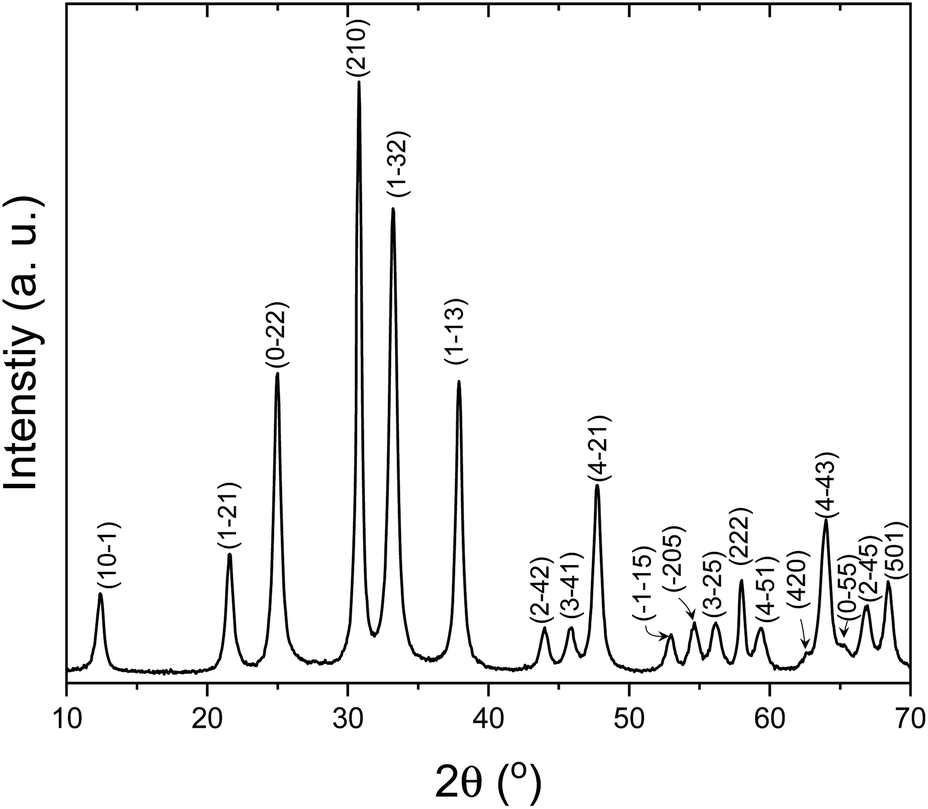
XRD was carried out on the as-synthesized nanoparticles, whose diffraction pattern is displayed in Fig. 1. All the diffraction peaks were perfectly indexed on the rhombohedral space group R![[3 with combining macron]](https://www.rsc.org/images/entities/char_0033_0304.gif) basis of Zn2GeO4 (ICSD Collection Code: 68382), with cell parameters a = b = 14.28 Å and c = 9.55 Å. This diffractogram clearly shows that nanocrystals possess a willemite-like structure32 compared to the Zn2GeO4 reference, where the structure can be described as formed of tetrahedrally coordinated zinc and germanium atoms, sharing corners.33 The absence of additional reflections, which could be attributed to impurities, is indicative of the remarkable purity of the Zn2GeO4 sample, even without the need for high-temperature thermal treatments. The relative wide maxima suggest the nanoparticle nature of the material.
basis of Zn2GeO4 (ICSD Collection Code: 68382), with cell parameters a = b = 14.28 Å and c = 9.55 Å. This diffractogram clearly shows that nanocrystals possess a willemite-like structure32 compared to the Zn2GeO4 reference, where the structure can be described as formed of tetrahedrally coordinated zinc and germanium atoms, sharing corners.33 The absence of additional reflections, which could be attributed to impurities, is indicative of the remarkable purity of the Zn2GeO4 sample, even without the need for high-temperature thermal treatments. The relative wide maxima suggest the nanoparticle nature of the material.
 | ||
| Fig. 1 Indexed XRD pattern of the as-synthesized Zn2GeO4 nanoparticles. | ||
The average crystal size has been calculated from the values of the form factor K, the wavelength of the incident radiation λ, the full width at half maximum B, the diffraction maximum {210}, and the diffraction angle θ, along with the Scherrer formula: D = Kλ/(B![[thin space (1/6-em)]](https://www.rsc.org/images/entities/char_2009.gif) cosθ). The mean value is 17 ± 0.02 nm.
cosθ). The mean value is 17 ± 0.02 nm.
To confirm these results, transmission electron microscopy studies have been carried out. The low-magnification TEM image depicted in Fig. 2a evidences that most nanoparticles possess a short rod-like morphology. Particle length and diameter distributions are presented in Fig. 2b and c, revealing their small size. Specifically, particle length ranges between 24 and 54 nm with an average length of 37 ± 7 nm, whilst their mean diameter stands at 13 ± 3 nm, varying from 7 to 19 nm. These values provide an aspect-ratio value of 1:3 for the nanorods. Particle size distributions have been constructed measuring 50 different nanoparticles.
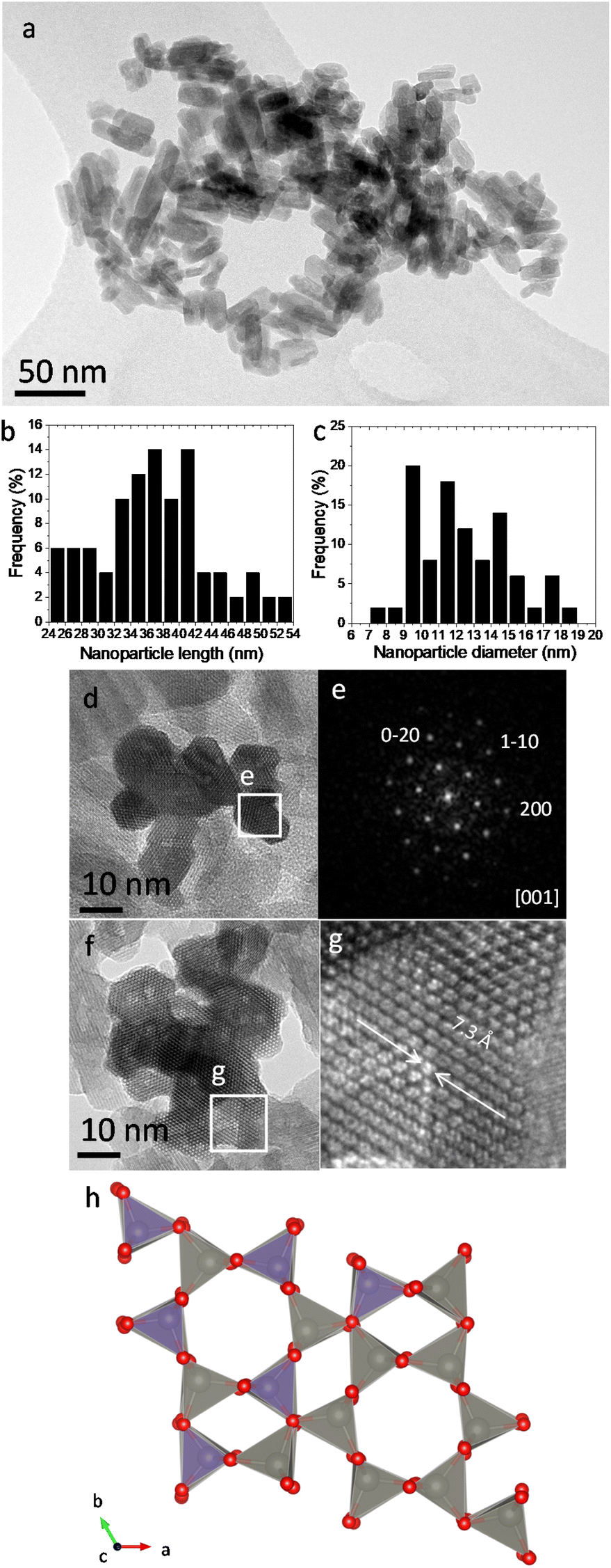 | ||
| Fig. 2 (a) Representative low magnification TEM image of the as-synthesized Zn2GeO4 nanoparticles. (b) and (c) Nanoparticle length and diameter distributions, respectively. (d) HRTEM top-view image of a Zn2GeO4 nanoparticle agglomerate. (e) DDP extracted from the region encircled in (d). (f) HRTEM top-view image of another Zn2GeO4 nanoparticle agglomerate, from which a magnified inset was extracted (g), evidencing the presence of the characteristic tunnels of the willemite-type structure of Zn2GeO4. (h) Crystallographic model of the Zn2GeO4 structure viewed along the [001] zone axis. | ||
In addition, our HRTEM studies confirm that the structure of the nanorods corresponds to rhombohedral willemite-like Zn2GeO4. Fig. 2d and f depict the electron micrograph top-view images of representative agglomerates of Zn2GeO4 nanocrystals oriented along the [001] zone axis. As suggested by these images, the radial morphology of these rod-like nanoparticles is greatly varied, but numerous cross-sections present 60° and 120° angles. Therefore, some of these nanoparticles may derive from distorted hexagonal and truncated triangular prismatic nanocrystals.
The digital diffraction pattern (DDP), extracted from one of the crystals (Fig. 2e) clearly shows the perfect willemite-like lattice of the nanocrystals. The reflection distances and angles measured are 3.6 Å at 60°, corresponding to {200}, {020} and {1−10} planes oriented along the [001] zone axis. On the other hand, the characteristic tunnels, inherent to the willemite structure and parallel to the [001]-axis direction, which are clearly observed in the graphical representation of the Zn2GeO4 structure displayed in Fig. 2h, can be readily discerned in Fig. 2g, which depicts a magnified region from Fig. 2f. The experimental diameter of the tunnels has been estimated using HRTEM images, and the measured values are approximately 7.3 Å, in accordance with the structure described for this oxide.32
Optical characterization of the nanoparticles
An in-depth study of the luminescence emission of the as-synthesized Zn2GeO4 nanoparticles was carried out. An analysis of the emission provides information about the electronic recombinations between conduction and valence bands or between the electronic levels caused by native defects within the bandgap. As a first step, room temperature luminescence of these Zn2GeO4 nanocrystals has been assessed. Fig. 3 shows the room temperature luminescence spectrum acquired with an He–Cd laser (λ = 325 nm). A broad visible band covering practically the whole visible range is observed. PL spectra agree with the complex nature of the luminescence band involving several radiative centres. The broad luminescence emission can be deconvoluted intro three components (2.18 eV, 2.41 eV and 2.81 eV), as previously reported in other Zn2GeO4 nanoparticles grown by a different synthesis method.18 The green-yellow broad band whose maximum is centred at 2.41 eV is the dominant contribution to the luminescence of this material. Li and co-workers34 have suggested that this complex band is related to Ge centres (bands peaked at 2.18 eV and 2.41 eV) and oxygen defects (band peaked at 2.8 eV). | ||
| Fig. 3 RT luminescence spectra from Zn2GeO4 nanorods excited by a 325nm UV laser. Gaussian emission bands after deconvolution (dotted lines) are shown. | ||
These emission contributions are very close to the ones reported for microrods, which have overall higher dimensions (1–2 microns wide and hundreds of microns length),16 and rather distinct from Zn2GeO4 nanoparticles, nanowires and Zn2GeO4 in bulk form.17,18,35
Particularly, the aspect ratio between the microrods prepared in our previous work16 and these nanorods is rather similar, but their overall dimensions are entirely distinct. Nevertheless, the nanoparticle size of the sample we synthesized in a previous paper18 (10 or 16 nm in average) is comparable to some of our nanorods, but with an aspect ratio close to 1:1. Hence, our results evidence that particles with similar morphologies, but clearly different particle sizes (nanorods and microrods) possess an analogous phosphor emission, which reinforces the relevant effect of morphology on the light emission efficiency of Zn2GeO4. Therefore, particle size preliminarily seems to play a minor role in the light emitting properties than particle morphology. Hence, by reducing the particle size we can provide several of the advantages of nanoparticles versus micro and bulk materials without drastically altering the luminescent response of the material.
This occurrence might be explained assuming the absence of charge carriers' confinement along the c zone axis in nanorods and microrods (due to their length) while this confinement is present along all crystallographic directions in Zn2GeO4 nanoparticles. The crystallographic anisotropic character of Zn2GeO4 could further reinforce this hypothesis. In this sense, previous literature has evidenced that Zn2GeO4 optical properties along the c axis, such as its refractive index and Raman signals, differ from the ones measured at the basal plane.36 Additionally, the competition between surface states and “volume” electronics sates would also affect the luminescence behaviour.
To understand better the origin of these emission bands, PL and PLE spectra were acquired at RT and at low temperature (4 K). Fig. 4 shows the contour plot PL–PLE mappings recorded at RT (Fig. 4a) and 4 K (Fig. 4b). In both cases, spectra were collected by varying the excitation wavelength between 250 and 285 nm (4.96–4.35 eV) in order to ensure an excitation energy over, or close to the bandgap energy to be used, while the light emitted was recorded between 320 and 650 nm (3.88–1.9 eV).
 | ||
| Fig. 4 PL–PLE maps acquired on the nanorods (a) at RT and (b) at 4 K. The color code employed for representing the relative PL–PLE intensity follows a rainbow-like trend: red corresponds to the highest normalized intensity, while violet pixels represent emission energies with the lowest relative intensities. | ||
Analysing the data from these emission maps, a broadening of the emission spectra occurs as temperature increases, along with a decrease of the overall luminescence intensity. Furthermore, it can be observed that the maximum emission of the sample occurs with an excitation in the range of 265–270 nm for 4 K, and that this range increases to 260–280 nm when the sample is at RT. Using an excitation with an energy above the gap of the material produces a UV emission centred between 320 and 400 nm (3.1–3.4 eV). Under these excitation conditions, an additional ultraviolet band centred at 3.4 eV is observed at low temperature. This band has been previously attributed to a recombination between VO related electronic levels and self-trapped holes.12 Therefore, the intensity of this band is directly related to oxygen vacancies. The overall PL spectrum observed in Fig. 5a is not composed of a unique emission band as shown in Fig. 5b. Deconvolution of the PL spectrum at 4 K shows that it is composed of five Gaussian emissions: three in the visible range (2.01 eV, 2.40 eV and 2.68 eV) and two Gaussian emissions in the ultraviolet range (3.11 eV and 3.47 eV), with 2.4 and 2.68 eV being the most representative in the visible region and 3.47 eV in the UV region. It is worth mentioning that this UV emission is quenched totally at 100–100 K, remaining only the visible band.
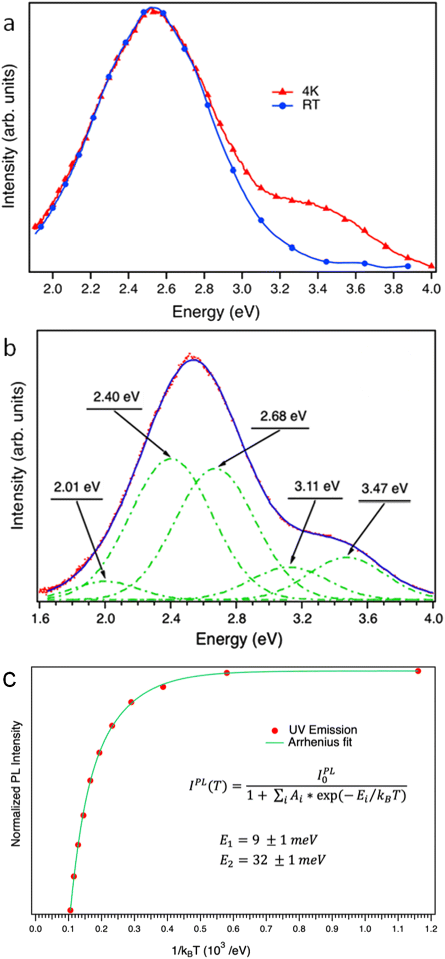 | ||
| Fig. 5 (a) Luminescence spectra, at 4 K and RT, form nanorods under 250 nm excitation wavelength of a xenon lamp. (b) Gaussian emission bands after deconvolution (dotted lines) of the spectrum acquired at 4 K are shown. (c) Temperature dependence of PL intensity emission. | ||
The temperature dependence of the PL intensity of emissions related to defect centers can be studied in an Arrhenius-plot scheme. The results for the UV emission are shown in Fig. 5c. From fitting this data to the empirical expression shown in the figure, the activation energies of non-radiative centres affecting the final radiative yield can be estimated. The results show that two levels are required to properly fit the experimental results, with activation energies of 8 ± 1 meV and 27 ± 1 meV. The channel associated with the lower energy supports an efficient emission at low temperature, but not upon 100 K, and the second channel is not relevant at this temperature range. For comparison, in the case of nanoparticles, values of 17 ± 1 and 84 ± 3 meV were obtained.18
Finally, our PL–PLE study allows us to estimate the optical band gap of the nanorods, since it is proportional to the absorption spectrum.37Fig. 6 shows the photoluminescence excitation spectrum (PLE) corresponding to the emission of the nanoparticles at 360 nm (3.44 eV) upon varying the excitation wavelength from 240 nm to 285 nm. By fitting the absorption onset, an estimation of the optical band gap of 4.77 eV at 4 K for our nanorods is provided. This value is analogous to that reported for microwires (4.76 eV). However, it is lower than the one reported for nanoparticles (4.85 eV) and thin films (4.9 eV)39 and higher in comparison with bulk Zn2GeO4 (4.68 eV).38 These results clearly evidence the influence of crystallite morphology on the optoelectronic properties of Zn2GeO4 as nanoparticles with radically different external shapes present rather distinctive optoelectronic responses.
 | ||
| Fig. 6 PLE spectrum at 4 K of the nanorods, from which the optical band gap is estimated. | ||
Conclusions
Zn2GeO4 short nanorods were successfully prepared by a reproducible hydrothermal synthesis. These nanorods are quite homogeneous in both particle size and morphology, with no impurities. A high number of nanostructures with about 1:3 aspect ratio are achieved. These nanomaterials become an intermediate step between nanoparticles of few nanometer diameter and nanowires with microns in length. PL spectra collected at both room temperature and at 4 K are rather wide, covering almost all the visible range being centred in the green-yellow region. Deconvolution of PL spectra brings about several components, which are attributed to donor–acceptor pair transitions involving native defects (oxygen vacancies as donors and zinc/germanium vacancies as acceptors). In addition, oxygen vacancies and self-hole traps produce UV emission at low temperatures upon excitation at energies above the excitation threshold and the emission is quenched around 120 K. The bandgap of Zn2GeO4 nanorods has been estimated as 4.77 eV, which is lower than the one reported for nanoparticles and higher in comparison with bulk Zn2GeO4. The results strongly reinforce that morphology and aspect-ratio are crucial parameters in the optoelectronic properties of Zn2GeO4.
Author contributions
MT and JRC: conceptualization; MT, JML and PH: methodology; MT and PH: formal analysis; MT and PH: investigation; MT and PH: writing – original draft; MT, PH and JRC: writing – review and editing; JMGC and BM: supervision; JMGC and BM: funding acquisition. All authors have read and agreed to the published version of the manuscript.Conflicts of interest
There are no conflicts to declare.Acknowledgements
The authors acknowledge the Spanish Ministry of Science and Innovation for funding through Research Projects PID 2020-113753RB-100 and PID2021-122562NB-I00.Notes and references
- J. A. Del Alamo, Nature, 2011, 479, 317–323 CrossRef CAS PubMed.
- A. Tanaka, Toxicol. Appl. Pharmacol., 2004, 198, 405–411 CrossRef CAS PubMed.
- C. R. Chitambar, Int. J. Environ. Res. Public Health, 2010, 7, 2337–2361 CrossRef CAS PubMed.
- M. Leng, Z. Chen, Y. Yang, Z. Li, K. Zeng, K. Li, G. Niu, Y. He, Q. Zhou and J. Tang, Angew. Chem., Int. Ed., 2016, 128, 15236–15240 CrossRef.
- A. M. Alfantazi and R. R. Moskalyk, Miner. Eng., 2003, 16, 687–694 CrossRef CAS.
- European Commission, First Commission Interim Report on the Implementation of Pilot Projects and Preparatory Actions 2012, 2012 Search PubMed.
- US Department of Energy, U.S. Department of Energy's Strategy to Support Domestic Critical Mineral to Support Domestic Critical Mineral and Material Supply Chain, 2021 Search PubMed.
- D. V. Bavykin, J. M. Friedrich and F. C. Walsh, Adv. Mater., 2006, 18, 2807–2824 CrossRef CAS.
- P. Roy, S. Berger and P. Schmuki, Angew. Chem., Int. Ed., 2011, 50, 2904–2939 CrossRef CAS PubMed.
- C. B. Ong, L. Y. Ng and A. W. Mohammad, Renewable Sustainable Energy Rev., 2018, 81, 536–551 CrossRef CAS.
- Z. L. Wang, J. Phys.: Condens. Matter, 2004, 16, R829 CrossRef CAS.
- Z. Liu, X. Jing and L. Wang, J. Electrochem. Soc., 2007, 154, H500 CrossRef CAS.
- Z. Y. Xie, H. L. Lu, Y. Zhang, Q. Q. Sun, P. Zhou, S. J. Ding and D. W. Zhang, J. Alloys Compd., 2015, 619, 368–371 CrossRef CAS.
- J. Dolado, R. Martínez-Casado, P. Hidalgo, R. Gutierrez, A. Dianat, G. Cuniberti, F. Domínguez-Adame, E. Díaz and B. Méndez, Acta Mater., 2020, 196, 626–634 CrossRef CAS.
- L. Yang, Z. Zhou, J. Song and X. Chen, Chem. Soc. Rev., 2019, 48, 5140–5176 RSC.
- P. Hidalgo, A. López, B. Méndez and J. Piqueras, Acta Mater., 2016, 104, 84–90 CrossRef CAS.
- J. Xu, C. Wang, Y. Zhang, X. Liu, X. Liu, S. Huang and X. Chen, CrystEngComm, 2013, 15, 764–768 RSC.
- J. Dolado, J. García-Fernández, P. Hidalgo, J. González-Calbet, J. Ramírez-Castellanos and B. Méndez, J. Alloys Compd., 2022, 898, 162993 CrossRef CAS.
- H. F. Wilson, L. McKenzie-Sell and A. S. Barnard, J. Mater. Chem. C, 2014, 2, 9451–9456 RSC.
- Q. Liu, Z. X. Low, L. Li, A. Razmjou, K. Wang, J. Yao and H. Wang, J. Mater. Chem. A, 2013, 1, 11563–11569 RSC.
- J. Huang, K. Ding, Y. Hou, X. Wang and X. Fu, ChemSusChem, 2008, 1, 1011–1019 CrossRef CAS PubMed.
- J. Wang, Q. Ma, W. Zheng, H. Liu, C. Yin, F. Wang, X. Chen, Q. Yuan and W. Tan, ACS Nano, 2017, 11, 8185–8191 CrossRef CAS PubMed.
- J. K. Feng, M. O. Lai and L. Lu, Electrochem. Commun., 2011, 13, 287–289 CrossRef CAS.
- Y. R. Lim, C. S. Jung, H. S. Im, K. Park, J. Park, W. Il Cho and E. H. Cha, J. Mater. Chem. A, 2016, 4, 10691–10699 RSC.
- Q. Liu, Y. Zhou, J. Kou, X. Chen, Z. Tian, J. Gao, S. Yan and Z. Zou, J. Am. Chem. Soc., 2010, 132, 14385–14387 CrossRef CAS PubMed.
- Z. Liu, H. Huang, B. Liang, X. Wang, Z. Wang, D. Chen and G. Shen, Opt. Express, 2012, 20, 2982–2991 CrossRef CAS PubMed.
- X. Zhou, Q. Zhang, L. Gan, X. Li, H. Li, Y. Zhang, D. Golberg and T. Zhai, Adv. Funct. Mater., 2016, 26, 704–712 CrossRef CAS.
- C. Yan and P. S. Lee, J. Phys. Chem. C, 2009, 113, 14135–14139 CrossRef CAS.
- Z. Gu, F. Liu, X. Li and Z. W. Pan, Phys. Chem. Chem. Phys., 2013, 15, 7488–7493 RSC.
- F. Chi, X. Wei, B. Jiang, Y. Chen, C. Duan and M. Yin, Dalton Trans., 2018, 47, 1303–1311 RSC.
- J. Liu, G. Zhang, J. C. Yu and Y. Guo, Dalton Trans., 2013, 42, 5092–5099 RSC.
- J. Breternitz, D. Fritsch, A. Franz and S. Schorr, Z. Anorg. Allg. Chem., 2021, 647, 2195–2200 CrossRef CAS.
- K.-H. Klaska, J. C. Eck and D. Pohl, Acta Crystallogr., 1978, 34, 3324–3325 CrossRef.
- L. Li, Y. Su, Y. Chen, M. Gao, Q. Chen and Y. Feng, J. Comput. Theor. Nanosci., 2010, 3, 1–5 Search PubMed.
- X. Duan, M. Yuan, K. Ou, W. Zhao, T. Tian, W. Duan, X. Zhang and L. Yi, Mater. Today Commun., 2021, 27, 102359 CrossRef CAS.
- J. Dolado, R. Martínez-Casado, P. Hidalgo and B. Méndez, Opt. Mater. Express, 2023, 13, 3156 CrossRef CAS.
- H. Masai, Y. Yamada, Y. Suzuki, K. Teramura, Y. Kanemitsu and T. Yoko, Sci. Rep., 2013, 3, 03541 CrossRef PubMed.
- C. Yan, N. Singh and P. S. Lee, Appl. Phys. Lett., 2010, 96, 053108 CrossRef.
- S. Luo, L. Trefflich, S. Selle, R. Hildebrandt, E. Krüger, S. Lange, J. Yu, C. Sturm, M. Lorenz, H. Von Wenckstern, C. Hagendorf, T. Höche and M. Grundmann, Appl. Phys. Lett., 2023, 122, 031601 CrossRef CAS.
| This journal is © The Royal Society of Chemistry 2024 |