
 Open Access Article
 This Open Access Article is licensed under a Creative Commons Attribution-Non Commercial 3.0 Unported Licence
Metrology for 2D materials: a perspective review from the international roadmap for devices and systems
Umberto
Celano
 *a,
Daniel
Schmidt
b,
Carlos
Beitia
c,
George
Orji
d,
Albert V.
Davydov
d and
Yaw
Obeng
d
*a,
Daniel
Schmidt
b,
Carlos
Beitia
c,
George
Orji
d,
Albert V.
Davydov
d and
Yaw
Obeng
d
aSchool of Electrical, Computer and Energy Engineering, Arizona State University, Tempe, AZ 85287, USA. E-mail: umberto.celano@asu.edu
bIBM Research, 257 Fuller Rd, Albany, NY 12203, USA
cUnity-SC, 611 Rue Aristide Berges, 38330 Montbonnot-Saint-Martin, France
dNational Institute of Standards and Technology, 100 Bureau Drive, Gaithersburg, MD, USA. E-mail: yaw.obeng@nist.gov
First published on 8th April 2024
Abstract
The International Roadmap for Devices and Systems (IRDS) predicts the integration of 2D materials into high-volume manufacturing as channel materials within the next decade, primarily in ultra-scaled and low-power devices. While their widespread adoption in advanced chip manufacturing is evolving, the need for diverse characterization methods is clear. This is necessary to assess structural, electrical, compositional, and mechanical properties to control and optimize 2D materials in mass-produced devices. Although the lab-to-fab transition remains nascent and a universal metrology solution is yet to emerge, rapid community progress underscores the potential for significant advancements. This paper reviews current measurement capabilities, identifies gaps in essential metrology for CMOS-compatible 2D materials, and explores fundamental measurement science limitations when applying these techniques in high-volume semiconductor manufacturing.
1. Introduction
Two-dimensional (2D) inorganic materials, such as graphene, black phosphorus (BP), hexagonal boron nitride (h-BN), and transition metal dichalcogenides (TMD) with a formula MX2, where M is a transition metal (such as Mo, W, etc.) and X is a chalcogen (S, Se, or Te), belong to a class of emerging ultra-thin layered materials comprised of one- to few-atomic layers linked by van der Waals forces.1–4 This class of materials shows superlative electrical, optical, mechanical, and thermal properties, among other intrinsic properties, that make them promising building blocks for the future of nanoelectronics. They are suitable for applications in both the front end of the line, where they are considered for ultra-scaled transistors focusing on high mobility and high on-state current, and in the back end of the line, where 2D materials should meet an increasing requirement for low thermal budget and low-power dissipation.5–10 In addition, numerous advancements have been made in the field of sensors, batteries, photovoltaics, and heterostructures with tailored optoelectronic features.11,12 The ultra-thin nature of these materials and their complex large-area synthesis pose unprecedented challenges in defect-free growth, transfer, process development, and metrology.13 The international roadmap of devices and systems projects that 2D materials will be inserted into high-volume manufacturing as channel materials, mostly for low-power applications, within the next 10 years.14,15As shown in Fig. 1, it could take over a decade for newly developed measurement techniques to be introduced to a high-volume manufacturing (HVM) process since they need to be developed into a tool with the precision, uncertainties, and operational stability required for the application. Fig. 1 indicates the trajectories of various measurement techniques that are directly applicable to the 2D material-based device process development for eventual introduction to HVM. Fig. 2 summarizes a multitude of characterization methods that are required to access, monitor, and tune the structural, electrical, compositional, and mechanical properties of 2D materials in mass-produced devices. In this paper, we critically review existing and emerging measurement capabilities, identify the gaps in key areas of dedicated metrology for CMOS-compatible 2D materials, and describe the fundamental measurement science limits associated with these techniques when applied to 2D materials for semiconductor manufacturing.
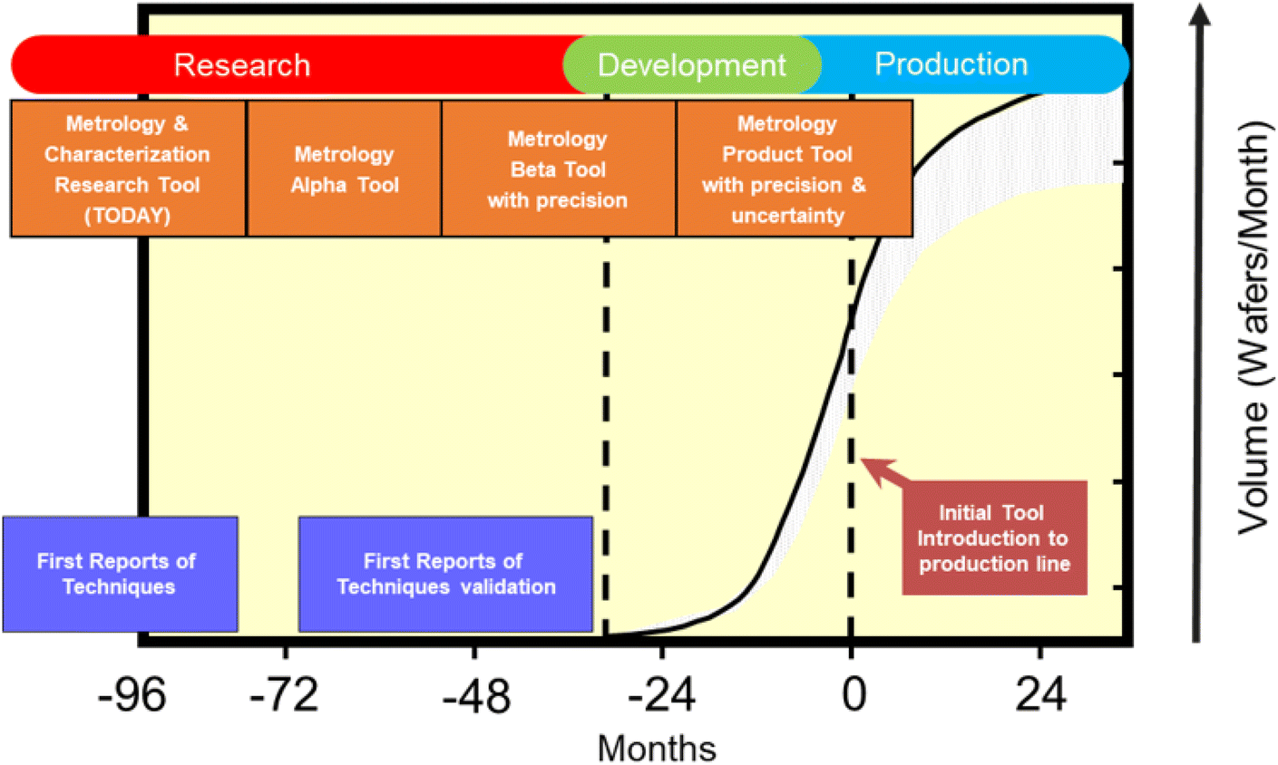 | ||
| Fig. 1 A typical production ramp curve for an established process, showing the timeframes of materials metrology tools from research to development to production. The top level of the curve indicates high-volume manufacturing (HVM). Note that studies validating the technique for its intended applications usually start to be presented at conferences five years or more before the technique is accepted for the HVM. | ||
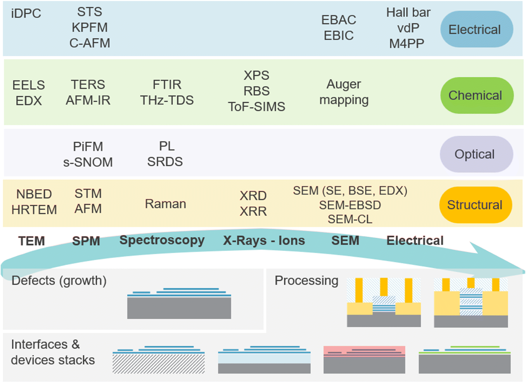 | ||
| Fig. 2 Overview of the 2D materials characterization methods reported in this review. | ||
2. Defects in 2D materials
Defects are inevitable in 2D materials.16 Two broad categories of defects, intrinsic and extrinsic, are encountered in 2D materials. For example, in a typical MoS2 system, intrinsic defects are generally introduced by the growth process and include vacancies, substitutional and ad-atoms, grain boundaries (GBs), dislocations, local oxidation, a mixture of polytypes, and strain, among others. Extrinsic defects are largely dependent on the selected substrate (e.g., Si, SiOx-on-Si, sapphire, etc.), and can affect the growth-related island control, phase-inhomogeneities, the presence of uncontrolled charges at the interface or in the bulk, which result in local variations of the band structure. In addition, polymer contamination (absorption and intercalation), strain, fractures, or delamination are all major sources of non-idealities for transferred material. Defects in 2D materials can be engineered to tailor functional properties such as light absorption, bandgap, and mobility. Therefore, it is fundamental to have quantitative methods for both defect engineering and characterization.16 Thus, as these materials become industrially relevant, the need for methodologies for screening key physical properties including but not limited to material quality, coverage, uniformity, defectivity, stacking order and orientation, layer numbers, contaminations, and interface control has become critical.13. Metrology for 2D materials
The reduced dimensions of “one or few-atoms thick” 2D materials and their easily perturbed physical properties entail that characterization techniques must have both nanoscale resolution and sensitivity to a range of properties, with minimal probe–sample interactions. As such, a host of complementary nanoscale measurement methods are used to study 2D materials, including scanning electron microscopy (SEM), scanning transmission electron microscopy (STEM) and scanning probe microscopies (SPMs), spectroscopic techniques, neutron scattering, and various surface science analytical techniques, among others.17 SEM techniques provide fast characterization of 2D materials from millimeter to nanometer scale, including surface morphology, crystal structure, and chemical composition. Working at low acceleration voltages and low beam currents allows non-destructive imaging of 2D layers to reveal their domain sizes and shapes, grain boundaries, surface imperfections, such as wrinkles and microcracks, and other morphological and structural defects. Combining secondary electron (SE) and backscattered electron (BSE) imaging with energy-dispersive X-ray (EDX) and electron backscatter diffraction (EBSD) analysis provides a full morphological, structural, and compositional characterization of 2D layers and device structures. The addition of spectroscopic capabilities to SEM instruments, such as cathodoluminescence (CL) enables in situ correlation of morphological, structural, and compositional imaging with electronic properties of 2D layers and heterostructures with high spatial and spectral resolution.18–20 STEM and SPM enable direct visualization and identification of disorder in the atomic arrangement of 2D materials crystals,21,22 while TEM-based analysis such as electron energy loss spectroscopy (EELS) and nanobeam electron diffraction (NBED) have been used to demonstrate the spectral response dependence of 2D materials to temperature, composition, number of layers, and to map strain.23–26 In addition, the limited scattering of the e-beam with atomically thin layers enables sub-angstrom resolution at low beam energies through ptychographic reconstruction in these materials. Dark-field TEM and 4D-STEM have been combined with machine learning (ML) based data segmentation to demonstrate grain structure orientation and stacking order analysis by using epitaxially grown bilayer MoS2.27 Interestingly, the observation of defect dynamics under e-beam irradiation inside a TEM can offer a useful analytical tool to monitor processes involving atomic rearrangements, such as material growth and thermally activated events. Importantly, recent work based on 4D-STEM with center of mass (CoM) images and annular dark field (ADF) have been used to extract the projected electron charge density in monolayer MoS2.28 Similarly, Wen et al., reported on the atomic scale structure and fluctuations of electric fields around edge atoms with different bonding states than bulk atoms in MoS2.29The broad family of SPM methods, including scanning tunneling microscopy (STM) and electrical atomic force microscopy (AFM), have shown the potential to identify local defects such as vacancies, adatoms, substitutional impurities, GBs, and to qualify their physical properties, as well as carrier donor/acceptor and scattering, trap, and recombination centers.30,31 The combination of STM and conductive atomic force microscopy (C-AFM) has enabled various studies to map variations of the surface conductivity while probing the impact of individual defects, even when buried in multi-layer structures.32,33
A. Spectroscopic techniques
For large-area inspection, optical techniques represent a promising metrology option where the physics of the interaction of light with 2D materials is leveraged into rapid and non-destructive methods to study structural, atomic, and electrical properties. While graphene is a semimetal with no bandgap and a wavelength-independent opacity of 2.3 ± 0.1%, other 2D materials are semiconductors with complementary properties including bandgap energies (i.e., in the range from 1 eV to 6 eV) with different optical resonances that give rise to characteristic optical absorption.34,35 These have allowed the use of calibrated optical spectroscopy to determine the number of layers by measuring the transmittance, reflectance, and absorptance spectra, including spectroscopic ellipsometry for thickness mapping at wafer level.36 Among the optical spectroscopic techniques, surface differential reflectivity spectroscopy (SDRS) has the simplest setup and high sensitivity, and several studies from fundamental surface optical properties characterization37 up to in situ real-time material growth monitoring have confirmed its applicability to those cases.38 More recently, SDRS has been demonstrated as a flexible and versatile tool for studying 2D material.39,40 In addition, the potential of having high throughput wafer level inspection has been demonstrated and it has been recently implemented for silicon on insulator (SOI) ultrathin layers monitoring.41,42 Thus, using such a technique with monolayer level sensitivity directly linked to surface optical transition may be a way to monitor in-line for changes of variation in optical properties of 2D materials. PL and SDRS comparison in different studies has highlighted the relevance of such approaches for group group-6 and group-7 TMDs (e.g., WS2, MoS2, WSe2, MoSe2, and ReSe2).43,44 The availability of ab initio modeling 2D materials properties can help to create a link between SDRS signal variations and material properties changes. Semi-empirical macroscopic models coupled with simulations under the assumption that wavelength (λ) is much larger than the layer thickness in the well-known Fresnel equations have been also demonstrated.45Thanks to the impact of defects on the lattice vibration and optical properties, far-field Raman and photoluminescence (PL) have found wide applications for probing the structural quality and electronic behavior of 2D materials. Spectral peak shifts associated with out-of-plane vibrational modes with Raman spectroscopy have been used to identify a change in layers in 2D materials. In semiconductive 2D materials, PL quantum yield and PL spectra can be used to provide structural information. For example, starting from variations in the electronic band structure,46 the indirect bandgap transition can be linked to layer number in MoS2 films. In addition, Raman and PL can be used to sense strain-induced optical effects and band structure modification, thus enabling the study of the effects of uniaxial and biaxial strain in many 2D materials.47–49 Low-temperature PL is considered a more quantitative method to sense defect concentration thanks to the reduction of phonon-stimulated excitations but is also affected by dielectric environment, laser intensity, and strain thus leaving open a large set of options for the data interpretation.50–53 Besides far-field Raman spectroscopy, which became available as an in-line technique recently,54 ellipsometry and XPS, which are used in-line, most other options presented here are relatively slow or destructive.
Tip-based techniques are not economical: they are slow, have limited throughput, and small fields of view. Inline AFM is available and used at least in the development phase; research efforts are underway to increase speed through sampling with many parallel tips to make it compatible with high-volume manufacturing. Furthermore, tip-enhanced spectroscopy or microscopy techniques including tip-enhanced Raman (TERS), scattering-type scanning near-field optical microscopy (s-SNOM),55,56 and tip-enhanced photoluminescence (TEPL) have been used to non-destructively estimate defect location, type, density, and inter-defect distance, beyond the diffraction-limit of purely optical probes. TEPL in combination with AFM and Kelvin probe force microscopy (KPFM) has also been used to observe changes in the indirect-to-direct band-gap transition as a function of a number of layers and contact potential difference (CPD) in MoS2.57 Similarly, plasmonic enhancement at the AFM tip has enabled TERS to probe strain and chemical information with sub-50 nm resolution as reported for various 2D materials.58–60 TERS has also been used to compare ion-bombarded and pristine MoS2 layers, thus demonstrating a clear sensitivity to defect density.61,62 Once identified, specific defects can be monitored in Raman spectral responses (TERS or far-field), defining references for process development based on peak shape change, position shift, and broadening.62
It is also important to understand the growth quality of 2D materials, and the introduction of contaminations during processing and handling, by factors such as the type of substrates, growth temperature, chemical precursor, and catalysts.63 For such applications, surface-sensitive analytical techniques such as time-of-flight secondary ion mass spectrometry (ToF-SIMS) and X-ray photoelectron spectroscopy (XPS) can be used to study absorbates, composition, etc. These techniques have also been applied, either alone or in combination with in situ transmission infrared absorption spectroscopy, to monitor layer-by-layer thickness and chemical structure evolution during thermal treatments.64–66 While most of the optical properties of 2D materials can be tuned through electrostatic gating, chemical doping, or encapsulation, the tuning also creates a plethora of parasitic responses that are not necessarily related to the crystal quality. For example, in PL the purported conversion of trion and exciton emission could also originate from surface contamination.51
These methods are classified into electrical, chemical, optical, and structural imaging, and structural mapping approaches, and grouped by families of measurement techniques. This is further categorized by application areas target respect to process flow integration for high-volume manufacturing future needs. iDPC: integrated differential phase contrast; STS: scanning tunneling spectroscopy; KPFM: Kelvin probe force microscopy; EBAC: electron beam absorbed current; EBIC: electron beam induced current; M4PP: scanning micro four-point probes; vdP: van der Pauw; C-AFM: conductive-atomic force microscopy; EELS: electron energy loss spectroscopy; EDX: energy dispersive X-ray spectroscopy; TERS: tip enhanced Raman spectroscopy; AFM-IR: atomic force microscopy-infra-red; FTIR: Fourier transform infrared spectroscopy; THz-TDS: terahertz time-domain spectroscopy; XPS: X-ray photoelectron spectroscopy; RBS: Rutherford backscattering spectrometry; ToF-SIMS: time-of-flight-secondary ion mass spectrometry; ICP-MS: inductively coupled plasma mass spectrometry; PL: photoluminescence; PiFM: photo-induced force microscopy; s-SNOM: scattering-type scanning near-field optical microscopy; SDRS: surface differential reflectivity spectroscopy; NBED: nanobeam electron diffraction; HRTEM: high resolution transmission electron microscopy; STM: scanning tunnelling microscopy; AFM: atomic force microscopy; XRD: X-ray diffraction; XRR: X-ray reflectivity; SEM – scanning electron microscopy with secondary electron (SE) and backscattered electron (BSE) imaging with energy-dispersive X-ray (EDX) analysis; SEM-EBSD and SEM-CL: scanning electron microscopy with electron backscatter diffraction (EBSD) and cathodoluminescence (CL) detectors; TEM: tunnelling electron microscopy; SPM: scanning probe microscopy.
X-ray diffraction (XRD), and reflectivity (XRR), are the most suitable techniques for studying and probing lattice spacing in crystals with periodically arranged atoms. These techniques have also been used to suggest the presence of multi-layered structures in exfoliated and synthetic 2D materials. However, the interpretation of the results such as in-plane and out-of-plane lattice spacing and quantitative layer numbers can often be complicated by misalignment in the sample orientation, poor uniformity in coverage of the 2D materials, and interaction of the X-rays with surrounding materials.67,68 X-ray techniques can be extended beyond 2D materials: synchrotron X-ray scanning tunneling microscopy (SX-STM) has been used to image and identify a single metal atom.69
B. Metrology for doped 2D materials
Conventional doping technologies are not directly transferable to the world of atomically thin layers and there are limited possibilities to apply conventional quantitative analysis methods.70 Leveraging electron–phonon interaction, carrier-dependent spectral responses in both Raman and PL have been investigated for the analysis of doping in 2D materials.71,72 Backside illumination Raman spectroscopic studies have been used to study the interaction/doping of 2D materials and metal thin films.48 Unfortunately, as the physics of electron–phonon interactions in 2D materials is affected by multiple extrinsic factors, it is generally difficult to unambiguously separate the effects of strain and carriers, or other film–substrate interactions.An alternative metrology option for studying doping in 2D materials is scanning micro four-point probes (M4PP), for sheet conductance mapping in thin films. The probes consist of four sharp metal-coated silicon cantilevers, with an electrode spacing in the range of a few μm, although sub-micron probes spacing is in consideration. When operating, a small, constant current is injected into the outer two probes, while the voltage difference between the inner two probes is measured. By applying the appropriate formula based on the probe spacing and material properties, the sheet resistance (Rs) of the material under the probes can be calculated. M4PP has been successfully applied to extract sheet conductance and material uniformity of CVD-grown graphene.73 The technique cannot be considered non-destructive since the probes could damage the 2D material surface during the measurement. A dedicated probe design has been proposed to reduce the applied contact pressure.74 However, as M4PP is designed for sheet conductance of metals and doped-Si, applications beyond graphene have had major limitations due to the intrinsically higher sheet resistance of other 2D materials. A design that uses a dedicated back-gated setup to enable the modulation of carrier density modulation during the probing of transition metal dichalcogenides has been applied to this problem.73 Since these are mostly engineering modifications and not physical limitations, M4PP can offer a suitable method to collect wafer scale and fully automated conductivity maps.
Another technique of interest is THz time-domain spectroscopy (THz-TDS), which is a non-contact, non-destructive, and non-ionizing technique with the potential for 2D mapping of electrical parameters such as sheet conductance, sheet resistance, mobility, carrier density, scattering time, refractive index, and substrate thickness.77,78 This technique has been used for the electrical characterization of graphene, where terahertz absorption is directly linked to electrical conductivity and mobility and has been validated by comparison to other electrical characterization techniques such as the van der Pauw method.79,80 Measurements can be performed in reflection or transmission mode and with varying polarization angles of the emitter and receiver (as in ellipsometry). As such, THz-TDS is a possible solution for the fast characterization of electrical parameters with no limitation on the sample size. However, care should be taken to avoid inadvertent absorption of the THz signal by the target wafer, which limits the selection of materials that can be used as substrate or encapsulation of the 2D layer of interest. The spot size of a THz beam, which is currently diffraction-limited, could be made smaller by using near-field solutions at the expense of speed and reduced field of view.81 For chemical doping and adsorbed molecules, Fourier transform infrared (FTIR) spectroscopy has been demonstrated as a promising option for functional groups that are IR-active.75 These can be sensed with a spatial resolution (ca. 10–20 nm) comparable to that of an AFM by using nano-FTIR spectroscopy, AFM-IR, and photo-induced force microscopy (PiFM) as recently demonstrated for graphene and MoSe2.82
4. Applications of 2D materials in advanced electronics
Two-dimensional (2D) transition metal dichalcogenides (TMDs) exhibit exciting properties and versatile material chemistry that can be engineered for application specificity. 2D materials can enable various functions (e.g., electronics, energy storage and conversion, sensor, photonic, and optoelectronic functions) due to their diverse physical properties. These properties are being investigated for potential applications in advanced electronic devices. For example, 2D materials exhibiting phase transitions could address the challenge of further miniaturization, resulting in more energy-efficient and faster memory devices. These materials may also be useful as copper barrier material in interconnects in integrated circuits based on considerations such as the feasibility of technology integration, compatibility with other advanced metals like cobalt and ruthenium, electromigration robustness, and radio-frequency signal transmission fidelity.83 Entropy is an extensive quantity and, thus, the volume reduction associated with a dimensionality change from 3D to 2D can lead to a substantial decrease in latent heat in phase change.84 Therefore, much less energy is required to induce a readable phase change in 2D materials compared with 3D materials. These phase transitions could have technological importance in thermal management in advanced interconnects.85 Furthermore, the high optical nonlinearity in 2D materials enables these layered materials to modulate light with superior performance and makes them suitable for high-purity quantum emitters and quantum optical switches possible for integrated quantum circuits with atomic thickness.86 Leveraging pump–probe spectroscopic concepts, all-optical active modulation has been demonstrated by exploiting different mechanisms such as Pauli blocking and optical doping. It is crucial to overcome the low light absorption in 2D materials to increase the modulation depth. Research in this area will benefit from THz spectroscopy.Although 2D materials are not ready for high-volume manufacturing (HVM) yet, they are actively being investigated for application-specific deployment in advanced electronics. The reduced vertical dimensions of graphene and other 2D materials amiable to further miniaturization of electronic (More–Moore), and prototypical devices based on this premise have been successfully demonstrated in field-effect transistors (FET), tunnel FET, neuromorphic, and logic circuits. Furthermore, Coulomb screening in 2D systems is significantly reduced; this allows strong binding and improved lifetime of interlayer excitons that result in intriguing new states and applications, such as high-temperature quantum behaviors like excitonic Bose–Einstein condensation, superfluidity, electron–hole liquid, valley, orbital, spin, and topology.87 Also, TMDs have large mobile carrier densities and can carry high currents.88 While attractive, the utility of 2D materials for HVM is currently limited by practical considerations. For example, the self-passivating nature of 2D material surfaces requires fabrication methods that yield non-ideal interfaces, be it dielectric or metal with resultant high current leakage and contact resistances.4
5. Summary and outlook
In summary, the emergence of 2D materials in manufacturing facilities brings new options for devices, as well as new challenges for large-area synthesis, integration, and metrology. While 2D materials will not replace silicon, the application-specific co-integration of such material with silicon CMOS technology should provide increased chip functionality and flexibility. For successful insertion into the manufacturing process, some of the metrology challenges highlighted above and the tools to address them will need to be available. We reviewed the state of metrology for 2D materials with emphasis on the monitoring of intrinsic and extrinsic material quality and efficient mapping of structural, electrical, and optical properties. The ability to sense structural properties such as layer numbers, coverage, and uniformity is important due to the polymorphic nature of 2D materials. However, localized imaging of individual atoms is useful for characterizing defects including type, densities, and impact on doping, but is generally not compatible with acquiring abundant information over large areas. Existing in-line techniques such as Raman spectroscopy, ellipsometry, XPS, and possibly AFM, for example, will become the characterization techniques of choice for metrology on dedicated targets on patterned wafers. M4PP, optical, and THz spectroscopy can be considered as wafer-scale alternatives due to their relatively larger spot sizes, but at lower resolution, speed, and sensitivity to heterostructures of 2D materials with tailored properties. Fig. 3 shows a mosaic of the experimental data from the metrology for 2D materials discussed in this review. The ability of these methods to meet the fast-paced needs of the semiconductor manufacturing environment will determine when 2D materials will be widely adopted in high-volume manufacturing. This “lab-to-fab transition” is still in the early stages, and we note that although a one-size-fits-all metrology solution does not exist yet, rapid progress has been made by the community in a relatively short timeframe, thus indicating exciting times ahead.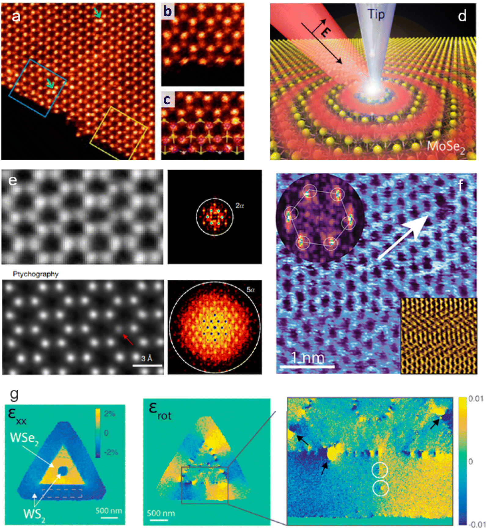 | ||
| Fig. 3 Mosaic of the experimental data from the state of metrology for 2D materials reported in this review. (a–c) Intrinsic point defects in monolayer MoS2 by STEM-ADF. (d) Schematic of nano-optical imaging study of waveguide MoSe2 using tip-enhanced SPM methods. (e) An electron microscope and pixel-array detector are used to record the complete distribution of transmitted electrons and full-field ptychography in MoS2. (f) Contact-mode electrical AFM is used to map barrier inhomogeneities in WS2. (g) Strain mapping at the WS2–WSe2 junction using an electron microscope pixel array detector (EMPAD) in TEM. Panels adapted with permission as follows: panel (a–c);22 panel (d);75 panel (e);76 panel (f);31 panel (g).26 | ||
Author contributions
All authors have contributed to the content selection, editing, and discussion of the manuscript during all phases of the preparation. All authors have approved the final version of the manuscript.Conflicts of interest
All authors declare no conflicts of interest or competing financial interests.References
- W. Choi, N. Choudhary, G. H. Han, J. Park, D. Akinwande and Y. H. Lee, Recent development of two-dimensional transition metal dichalcogenides and their applications, Mater. Today, 2017, 20(3), 116–130 CrossRef CAS.
- S. Manzeli, D. Ovchinnikov, D. Pasquier, O. V. Yazyev and A. Kis, 2D transition metal dichalcogenides, Nat. Rev. Mater., 2017, 2, 17033, DOI:10.1038/natrevmats.2017.33.
- W. Zhu, T. Low, H. Wang, P. Ye and X. Duan, Nanoscale electronic devices based on transition metal dichalcogenides, 2D Mater., 2019, 6(3), 032004, DOI:10.1088/2053-1583/ab1ed9.
- M. C. Lemme, D. Akinwande, C. Huyghebaert and C. Stampfer, 2D materials for future heterogeneous electronics, Nat. Commun., 2022, 13(1), 1392, DOI:10.1038/s41467-022-29001-4.
- C. Dorow, K. O'Brien, C. H. Naylor, S. Lee, A. Penumatcha, A. Hsiao, T. Tronic, M. Christenson, K. Maxey and H. Zhu, et al., Advancing Monolayer 2-D nMOS and pMOS Transistor Integration From Growth to Van Der Waals Interface Engineering for Ultimate CMOS Scaling, IEEE Trans. Electron Devices, 2021, 68(12), 6592–6598, DOI:10.1109/TED.2021.3118659.
- D. Akinwande, C. Huyghebaert, C. H. Wang, M. I. Serna, S. Goossens, L. J. Li, H. S. P. Wong and F. H. L. Koppens, Graphene and two-dimensional materials for silicon technology, Nature, 2019, 573(7775), 507–518, DOI:10.1038/s41586-019-1573-9.
- X. Xiong, A. Tong, X. Wang, S. Liu, X. Li, R. Huang, Y. Wu, Demonstration of Vertically-stacked CVD Monolayer Channels: MoS2 Nanosheets GAA-FET with Ion > 700 μA/μm and MoS2/WSe2 CFET, IEEE International Electron Devices Meeting (IEDM), San Francisco, CA, USA, 2021, pp. 7.5.1–7.5.4, DOI:10.1109/IEDM19574.2021.9720533.
- S. Das, A. Sebastian, E. Pop, C. J. McClellan, A. D. Franklin, T. Grasser, T. Knobloch, Y. Illarionov, A. V. Penumatcha and J. Appenzeller, et al., Transistors based on two-dimensional materials for future integrated circuits, Nat. Electron., 2021, 4(11), 786–799, DOI:10.1038/s41928-021-00670-1.
- M. Lanza and I. Radu, Electronic Circuits Made of 2D Materials, Wiley Online Library, 2022, vol. 34, p. 2207843 Search PubMed.
- C. Naylor, K. Maxey, C. Jezewski, K. O'Brien, A. Penumatcha, M. Kavrik, B. Agrawal, C. Littlefield, J. Lux and B. Barley, 2D materials in the BEOL, in 2023 IEEE Symposium on VLSI Technology and Circuits (VLSI Technology and Circuits), IEEE, 2023, pp. 1–2 Search PubMed.
- H. R. Gutiérrez, Two-dimensional layered materials offering expanded applications in flatland, ACS Appl. Nano Mater., 2020, 3(7), 6134–6139 CrossRef.
- T. Vincent, J. Liang, S. Singh, E. G. Castanon, X. Zhang, A. McCreary, D. Jariwala, O. Kazakova and Z. Y. Al Balushi, Opportunities in electrically tunable 2D materials beyond graphene: recent progress and future outlook, Appl. Phys. Rev., 2021, 8(4), 041320 CAS.
- N. Briggs, et.al., A Roadmap for Electronic Grade 2-dimensional Materials, 2D Mater, 2019, 6, 022001 CrossRef CAS.
- The International Roadmap of Semiconductors and Devices (IRDS), Beyond CMOS, 2021 Search PubMed.
- The International Roadmap of Semiconductors and Devices (IRDS), Metrology, 2021 Search PubMed.
- F. Liu and Z. Fan, Defect engineering of two-dimensional materials for advanced energy conversion and storage, Chem. Soc. Rev., 2023, 52, 1723–1772 RSC.
- A. McCreary, O. Kazakova, D. Jariwala and Z. Y. Al Balushi, An outlook into the flat land of 2D materials beyond graphene: synthesis, properties and device applications, 2D Mater., 2021, 8(1), 013001, DOI:10.1088/2053-1583/abc13d.
- S. Zheng, J.-K. So, F. Liu, Z. Liu, N. Zheludev and H. J. Fan, Giant enhancement of cathodoluminescence of monolayer transitional metal dichalcogenides semiconductors, Nano Lett., 2017, 17(10), 6475–6480 CrossRef CAS PubMed.
- H. Ramsden, S. Sarkar, Y. Wang, Y. Zhu, J. Kerfoot, E. M. Alexeev, T. Taniguchi, K. Watanabe, S. Tongay and A. C. Ferrari, Nanoscale Cathodoluminescence and Conductive Mode Scanning Electron Microscopy of van der Waals Heterostructures, ACS Nano, 2023, 17(12), 11882–11891 CrossRef CAS PubMed.
- M. Negri, L. Francaviglia, D. Dumcenco, M. Bosi, D. Kaplan, V. Swaminathan, G. Salviati, A. Kis, F. Fabbri and A. Fontcuberta I Morral, Quantitative Nanoscale Absorption Mapping: A Novel Technique to Probe Optical Absorption of Two-Dimensional Materials, Nano Lett., 2020, 20(1), 567–576 CrossRef CAS PubMed.
- D. Hsieh, T. Tsai, S. Huang, Y. Yang, C. Yang, J. Wu, J. Dai, J. Chen, J. Tan and P. Mukundhan, Characterization of high-K/metal gate using picosecond ultrasonics, Microelectron. Eng., 2011, 88(5), 583–588 CrossRef CAS.
- W. Zhou, X. Zou, S. Najmaei, Z. Liu, Y. Shi, J. Kong, J. Lou, P. M. Ajayan, B. I. Yakobson and J.-C. Idrobo, Intrinsic Structural Defects in Monolayer Molybdenum Disulfide, Nano Lett., 2013, 13(6), 2615–2622, DOI:10.1021/nl4007479.
- J. Hong, Z. Hu, M. Probert, K. Li, D. Lv, X. Yang, L. Gu, N. Mao, Q. Feng and L. Xie, et al., Exploring atomic defects in molybdenum disulphide monolayers, Nat. Commun., 2015, 6, 1–8, DOI:10.1038/ncomms7293.
- L. H. G. Tizei, Y.-C. Lin, A.-Y. Lu, L.-J. Li and K. Suenaga, Electron energy loss spectroscopy of excitons in two-dimensional-semiconductors as a function of temperature, Appl. Phys. Lett., 2016, 108(16), 163107, DOI:10.1063/1.4947058.
- Y.-Y. Chang, H. N. Han and M. Kim, Analyzing the microstructure and related properties of 2D materials by transmission electron microscopy, Appl. Microsc., 2019, 49(1), 10, DOI:10.1186/s42649-019-0013-5.
- Y. Han, K. Nguyen, M. Cao, P. Cueva, S. Xie, M. W. Tate, P. Purohit, S. M. Gruner, J. Park and D. A. Muller, Strain Mapping of Two-Dimensional Heterostructures with Subpicometer Precision, Nano Lett., 2018, 18(6), 3746–3751, DOI:10.1021/acs.nanolett.8b00952.
- A. N. Mehta, N. Gauquelin, M. Nord, A. Orekhov, H. Bender, D. Cerbu, J. Verbeeck and W. Vandervorst, Unravelling stacking order in epitaxial bilayer MX2 using 4D-STEM with unsupervised learning, Nanotechnology, 2020, 31(44), 445702 CrossRef CAS PubMed.
- J. Martis, S. Susarla, A. Rayabharam, C. Su, T. Paule, P. Pelz, C. Huff, X. Xu, H.-K. Li and M. Jaikissoon, Imaging the electron charge density in monolayer MoS2 at the Ångstrom scale, Nat. Commun., 2023, 14(1), 4363 CrossRef CAS PubMed.
- Y. Wen, S. Fang, M. Coupin, Y. Lu, C. Ophus, E. Kaxiras and J. H. Warner, Mapping 1D Confined Electromagnetic Edge States in 2D Monolayer Semiconducting MoS2 Using 4D-STEM, ACS Nano, 2022, 16(4), 6657–6665, DOI:10.1021/acsnano.2c01170.
- F. Giannazzo, E. Schilirò, G. Greco and F. Roccaforte, Conductive atomic force microscopy of semiconducting transition metal dichalcogenides and heterostructures, Nanomaterials, 2020, 10(4), 1–21, DOI:10.3390/nano10040803.
- K. Nowakowski, H. J. W. Zandvliet and P. Bampoulis, Barrier Inhomogeneities in Atomic Contacts on WS2, Nano Lett., 2019, 19(2), 1190–1196, DOI:10.1021/acs.nanolett.8b04636.
- C. Musumeci, Advanced Scanning Probe Microscopy of Graphene and Other 2D Materials, Crystals, 2017, 7(7), 216, DOI:10.3390/cryst7070216.
- J. Ludwig, A. N. Mehta, M. Mascaro, U. Celano, D. Chiappe, H. Bender, W. Vandervorst and K. Paredis, Effects of buried grain boundaries in multilayer MoS2, Nanotechnology, 2019, 30(28), 285705, DOI:10.1088/1361-6528/ab142f.
- Y. C. Lee, S. W. Chang, S. H. Chen, S. L. Chen and H. L. Chen, Optical Inspection of 2D Materials: From Mechanical Exfoliation to Wafer-Scale Growth and Beyond, Advanced Science, 2022, 9(1), 2102128, DOI:10.1002/advs.202102128.
- R. R. Nair, P. Blake, A. N. Grigorenko, K. S. Novoselov, T. J. Booth, T. Stauber, N. M. R. Peres and A. K. Geim, Fine Structure Constant Defines Visual Transparency of Graphene, Science, 2008, 320(5881), 1308, DOI:10.1126/science.1156965.
- A. Crovetto, P. R. Whelan, R. Wang, M. Galbiati, S. Hofmann and L. Camilli, Nondestructive Thickness Mapping of Wafer-Scale Hexagonal Boron Nitride Down to a Monolayer, ACS Appl. Mater. Interfaces, 2018, 10(30), 25804–25810, DOI:10.1021/acsami.8b08609.
- J. D. E. McIntyre and D. E. Aspnes, Differential reflection spectroscopy of very thin surface films, Surf. Sci., 1971, 24(2), 417–434, DOI:10.1016/0039-6028(71)90272-X.
- H. Qi and X. Fu, An In Situ Spectral Monitoring Scheme for Advanced Manufacturing of Novel Nanodevices, J. Sens., 2022, 2022, 1–10, DOI:10.1155/2022/4022440.
- R. Frisenda, Y. Niu, P. Gant, A. J. Molina-Mendoza, R. Schmidt, R. Bratschitsch, J. Liu, L. Fu, D. Dumcenco and A. Kis, et al., Micro-reflectance and transmittance spectroscopy: a versatile and powerful tool to characterize 2D materials, J. Phys. D: Appl. Phys., 2017, 50(7), 074002, DOI:10.1088/1361-6463/aa5256.
- C. Tsakonas, A. C. Manikas, M. Andersen, M. Dimitropoulos, K. Reuter and C. Galiotis, In situ kinetic studies of CVD graphene growth by reflection spectroscopy, Chem. Eng. J., 2021, 421, 129434, DOI:10.1016/j.cej.2021.129434.
- J. M. Billiez and W. Schwarzenbach, Differential reflective metrology an innovative variability measurement for advanced FDSOI material, in 2020 21st International Conference on Thermal, Mechanical and Multi-Physics Simulation and Experiments in Microelectronics and Microsystems (EuroSimE), IEEE, 2020, pp. 1–2, DOI:10.1109/EuroSimE48426.2020.9152621.
- Y. Niu, S. Gonzalez-Abad, R. Frisenda, P. Marauhn, M. Drüppel, P. Gant, R. Schmidt, N. Taghavi, D. Barcons and A. Molina-Mendoza, et al., Thickness-Dependent Differential Reflectance Spectra of Monolayer and Few-Layer MoS2, MoSe2, WS2 and WSe2, Nanomaterials, 2018, 8(9), 725, DOI:10.3390/nano8090725.
- E. Lorchat, L. E. P. López, C. Robert, D. Lagarde, G. Froehlicher, T. Taniguchi, K. Watanabe, X. Marie and S. Berciaud, Filtering the photoluminescence spectra of atomically thin semiconductors with graphene, Nat. Nanotechnol., 2020, 15(4), 283–288, DOI:10.1038/s41565-020-0644-2.
- O. B. Aslan, D. A. Chenet, A. M. van der Zande, J. C. Hone and T. F. Heinz, Linearly Polarized Excitons in Single- and Few-Layer ReS2 Crystals, ACS Photonics, 2016, 3(1), 96–101, DOI:10.1021/acsphotonics.5b00486.
- P. Adamson, Reflectance calculations of anisotropic dielectric constants of graphene-like two-dimensional materials, Appl. Opt., 2017, 56(28), 7832, DOI:10.1364/AO.56.007832.
- P. K. Chow, R. B. Jacobs-Gedrim, J. Gao, T.-M. Lu, B. Yu, H. Terrones and N. Koratkar, Defect-Induced Photoluminescence in Monolayer Semiconducting Transition Metal Dichalcogenides, ACS Nano, 2015, 9(2), 1520–1527, DOI:10.1021/nn5073495.
- A. M. Dadgar, D. Scullion, K. Kang, D. Esposito, E. H. Yang, I. P. Herman, M. A. Pimenta, E. J. G. Santos and A. N. Pasupathy, Strain Engineering and Raman Spectroscopy of Monolayer Transition Metal Dichalcogenides, Chem. Mater., 2018, 30(15), 5148–5155, DOI:10.1021/acs.chemmater.8b01672.
- A. Agyapong, K. Cooley and S. Mohney, Reactivity of contact metals on monolayer WS2, J. Appl. Phys., 2020, 128(5), 055306 CrossRef CAS.
- K. Q. Lin, J. Holler, J. M. Bauer, P. Parzefall, M. Scheuck, B. Peng, T. Korn, S. Bange, J. M. Lupton and C. Schüller, Large-Scale Mapping of Moiré Superlattices by Hyperspectral Raman Imaging, Adv. Mater., 2021, 33(34), 1–7, DOI:10.1002/adma.202008333.
- R. Abbaspour, D. Brown and M. Bakir, Fabrication and electrical characterization of sub-micron diameter through-silicon via for heterogeneous three-dimensional integrated circuits, J. Micromech. Microeng., 2017, 27(2), 025011 CrossRef.
- S. Anantachaisilp, S. M. Smith, C. Ton-That, T. Osotchan, A. R. Moon and M. R. Phillips, Tailoring deep level surface defects in ZnO nanorods for high sensitivity ammonia gas sensing, J. Phys. Chem. C, 2014, 118(46), 27150–27156 CrossRef CAS.
- I.-C. Hoi, C. Wilson, G. Johansson, J. Lindkvist, B. Peropadre, T. Palomaki and P. Delsing, Microwave quantum optics with an artificial atom in one-dimensional open space, New J. Phys., 2013, 15(2), 025011 CrossRef.
- J. W. Christopher, B. B. Goldberg and A. K. Swan, Long tailed trions in monolayer MoS2: temperature dependent asymmetry and resulting red-shift of trion photoluminescence spectra, Sci. Rep., 2017, 7(1), 14062, DOI:10.1038/s41598-017-14378-w.
- D. Schmidt, C. Durfee, J. Li, N. Loubet, A. Cepler, L. Neeman, N. Meir, J. Ofek, Y. Oren and D. Fishman, In-line Raman spectroscopy for gate-all-around nanosheet device manufacturing, J. Micro/Nanopatterning, Mater., Metrol., 2022, 21(2), 021203, DOI:10.1117/1.JMM.21.2.021203.
- G. A. Ermolaev, D. V. Grudinin, Y. V. Stebunov, K. V. Voronin, V. G. Kravets, J. Duan, A. B. Mazitov, G. I. Tselikov, A. Bylinkin and D. I. Yakubovsky, et al., Giant optical anisotropy in transition metal dichalcogenides for next-generation photonics, Nat. Commun., 2021, 12(1), 854, DOI:10.1038/s41467-021-21139-x.
- S. Dai, J. Quan, G. Hu, C. W. Qiu, T. H. Tao, X. Li and A. Alù, Hyperbolic Phonon Polaritons in Suspended Hexagonal Boron Nitride, Nano Lett., 2019, 19(2), 1009–1014, DOI:10.1021/acs.nanolett.8b04242.
- Y. Okuno, O. Lancry, A. Tempez, C. Cairone, M. Bosi, F. Fabbri and M. Chaigneau, Probing the nanoscale light emission properties of a CVD-grown MoS2 monolayer by tip-enhanced photoluminescence, Nanoscale, 2018, 10(29), 14055–14059, 10.1039/C8NR02421A.
- Z. Zhang, A. C. De Palma, C. J. Brennan, G. Cossio, R. Ghosh, S. K. Banerjee and E. T. Yu, Probing nanoscale variations in strain and band structure of MoS2 on Au nanopyramids using tip-enhanced Raman spectroscopy, Phys. Rev. B, 2018, 97(8), 085305, DOI:10.1103/PhysRevB.97.085305.
- P. Verma, Tip-Enhanced Raman Spectroscopy: Technique and Recent Advances, Chem. Rev., 2017, 117(9), 6447–6466, DOI:10.1021/acs.chemrev.6b00821.
- P. K. Sahoo, H. Zong, J. Liu, W. Xue, X. Lai, H. R. Gutiérrez and D. V. Voronine, Probing nano-heterogeneity and aging effects in lateral 2D heterostructures using tip-enhanced photoluminescence, Opt. Mater. Express, 2019, 9(4), 1620, DOI:10.1364/OME.9.001620.
- W. M. Parkin, A. Balan, L. Liang, P. M. Das, M. Lamparski, C. H. Naylor, J. A. Rodríguez-Manzo, A. T. C. Johnson, V. Meunier and M. Drndić, Raman Shifts in Electron-Irradiated Monolayer MoS2, ACS Nano, 2016, 10(4), 4134–4142, DOI:10.1021/acsnano.5b07388.
- F. Aryeetey, T. Ignatova and S. Aravamudhan, Quantification of defects engineered in single layer MoS2, RSC Adv., 2020, 10(39), 22996–23001, 10.1039/D0RA03372C.
- S. Caneva, R. S. Weatherup, B. C. Bayer, B. Brennan, S. J. Spencer, K. Mingard, A. Cabrero-Vilatela, C. Baehtz, A. J. Pollard and S. Hofmann, Nucleation Control for Large, Single Crystalline Domains of Monolayer Hexagonal Boron Nitride via Si-Doped Fe Catalysts, Nano Lett., 2015, 15(3), 1867–1875, DOI:10.1021/nl5046632.
- D. Y. Zemlyanov, M. Jespersen, D. N. Zakharov, J. Hu, R. Paul, A. Kumar, S. Pacley, N. Glavin, D. Saenz and K. C. Smith, et al., Versatile technique for assessing thickness of 2D layered materials by XPS, Nanotechnology, 2018, 29(11), 115705, DOI:10.1088/1361-6528/aaa6ef.
- M. Acik, G. Lee, C. Mattevi, A. Pirkle, R. M. Wallace, M. Chhowalla, K. Cho and Y. Chabal, The Role of Oxygen during Thermal Reduction of Graphene Oxide Studied by Infrared Absorption Spectroscopy, J. Phys. Chem. C, 2011, 115(40), 19761–19781, DOI:10.1021/jp2052618.
- I. H. Abidi, L.-T. Weng, C. P. J. Wong, A. Tyagi, L. Gan, Y. Ding, M. Li, Z. Gao, R. Xue and M. D. Hossain, et al., New Approach to Unveiling Individual Atomic Layers of 2D Materials and Their Heterostructures, Chem. Mater., 2018, 30(5), 1718–1728, DOI:10.1021/acs.chemmater.7b05371.
- M. Chubarov, T. H. Choudhury, X. Zhang and J. M. Redwing, In-plane X-ray diffraction for characterization of monolayer and few-layer transition metal dichalcogenide films, Nanotechnology, 2018, 29(5), 055706, DOI:10.1088/1361-6528/aaa1bd.
- F. Carrascoso, G. Sánchez-Santolino, C.-w. Hsu, N. M. Nemes, A. Torres-Pardo, P. Gant, F. J. Mompeán, K. Kalantar-zadeh, J. A. Alonso and M. García-Hernández, et al., Direct Transformation of Crystalline MoO3 into Few-Layers MoS2, Materials, 2020, 13(10), 2293, DOI:10.3390/ma13102293.
- T. M. Ajayi, N. Shirato, T. Rojas, S. Wieghold, X. Cheng, K. Z. Latt, D. J. Trainer, N. K. Dandu, Y. Li and S. Premarathna, et al., Characterization of just one atom using synchrotron X-rays, Nature, 2023, 618(7963), 69–73, DOI:10.1038/s41586-023-06011-w.
- Z. Wang, H. Xia, P. Wang, X. Zhou, C. Liu, Q. Zhang, F. Wang, M. Huang, S. Chen and P. Wu, et al., Controllable Doping in 2D Layered Materials, Adv. Mater., 2021, 33(48), 2104942, DOI:10.1002/adma.202104942.
- A. Das, S. Pisana, B. Chakraborty, S. Piscanec, S. K. Saha, U. V. Waghmare, K. S. Novoselov, H. R. Krishnamurthy, A. K. Geim, A. C. Ferrari and A. K. Sood, Monitoring dopants by Raman scattering in an electrochemically top-gated graphene transistor, Nat. Nanotechnol., 2008, 3(4), 210–215, DOI:10.1038/nnano.2008.67.
- M. W. Iqbal, K. Shahzad, G. Hussain, M. K. Arshad, R. Akbar, S. Azam, S. Aftab, T. Alharbi and A. Majid, Gate dependent phonon shift in tungsten disulfide (WS2) field effect transistor, Mater. Res. Express, 2019, 6(11), 115909, DOI:10.1088/2053-1591/ab485a.
- D. M. A. MacKenzie, K. G. Kalhauge, P. R. Whelan, F. W. Stergaard, I. Pasternak, W. Strupinski, P. Bøggild, P. U. Jepsen and D. H. Petersen, Wafer-scale graphene quality assessment using micro four-point probe mapping, Nanotechnology, 2020, 31(22), 225709, DOI:10.1088/1361-6528/ab7677.
- K. G. Kalhauge, H. H. Henrichsen, F. Wang, O. Hansen and D. H. Petersen, Vibration tolerance of micro-electrodes, J. Micromech. Microeng., 2018, 28(9), 095010, DOI:10.1088/1361-6439/aac58e.
- V. Mazánek, O. Jankovský, J. Luxa, D. Sedmidubský, Z. Janoušek, F. Šembera, M. Mikulics and Z. Sofer, Tuning of fluorine content in graphene: towards large-scale production of stoichiometric fluorographene, Nanoscale, 2015, 7(32), 13646–13655, 10.1039/C5NR03243A.
- Y. Jiang, Z. Chen, Y. Han, P. Deb, H. Gao, S. Xie, P. Purohit, M. W. Tate, J. Park and S. M. Gruner, et al., Electron ptychography of 2D materials to deep sub-ångström resolution, Nature, 2018, 559(7714), 343–349, DOI:10.1038/s41586-018-0298-5.
- C. J. Docherty, P. Parkinson, H. J. Joyce, M.-H. Chiu, C.-H. Chen, M.-Y. Lee, L.-J. Li, L. M. Herz and M. B. Johnston, Ultrafast Transient Terahertz Conductivity of Monolayer MoS2 and WSe2 Grown by Chemical Vapor Deposition, ACS Nano, 2014, 8(11), 11147–11153, DOI:10.1021/nn5034746.
- P. R. Whelan, B. Zhou, O. Bezencenet, A. Shivayogimath, N. Mishra, Q. Shen, B. S. Jessen, I. Pasternak, D. M. A. Mackenzie and J. Ji, et al., Case studies of electrical characterisation of graphene by terahertz time-domain spectroscopy, 2D Mater., 2021, 8, 022003, DOI:10.1088/2053-1583/abdbcb.
- P. Bøggild, D. M. A. Mackenzie, P. R. Whelan, D. H. Petersen, J. D. Buron, A. Zurutuza, J. Gallop, L. Hao and P. U. Jepsen, Mapping the electrical properties of large-area graphene, 2D Mater., 2017, 4(4), 042003, DOI:10.1088/2053-1583/aa8683.
- Z. Chen, C. Xie, W. Wang, J. Zhao, B. Liu, J. Shan, X. Wang, M. Hong, L. Lin and L. Huang, et al., Direct growth of wafer-scale highly oriented graphene on sapphire, Sci. Adv., 2021, 7(47) DOI:10.1126/sciadv.abk0115.
- S. Mastel, M. B. Lundeberg, P. Alonso-González, Y. Gao, K. Watanabe, T. Taniguchi, J. Hone, F. H. Koppens, A. Y. Nikitin and R. Hillenbrand, Terahertz nanofocusing with cantilevered terahertz-resonant antenna tips, Nano Lett., 2017, 17(11), 6526–6533 CrossRef CAS PubMed.
- J. Liu, S. Park, D. Nowak, M. Tian, Y. Wu, H. Long, K. Wang, B. Wang and P. Lu, Near-Field Characterization of Graphene Plasmons by Photo-Induced Force Microscopy, Laser Photonics Rev., 2018, 12(8), 1800040, DOI:10.1002/lpor.201800040.
- C.-L. Lo, B. A. Helfrecht, Y. He, D. M. Guzman, N. Onofrio, S. Zhang, D. Weinstein, A. Strachan and Z. Chen, Opportunities and challenges of 2D materials in back-end-of-line interconnect scaling, J. Appl. Phys., 2020, 128(8), 080903 CrossRef CAS.
- W. Li, X. Qian and J. Li, Phase transitions in 2D materials, Nat. Rev. Mater., 2021, 6(9), 829–846 CrossRef CAS.
- F. Sarvar, D. C. Whalley and P. P. Conway, Thermal interface materials-a review of the state of the art, in 2006 1st Electronic Systemintegration Technology Conference, IEEE, 2006, vol. 2, pp. 1292–1302 Search PubMed.
- Z. Sun, A. Martinez and F. Wang, Optical modulators with 2D layered materials, Nat. Photonics, 2016, 10(4), 227–238 CrossRef CAS.
- X. Zou, Y. Xu and W. Duan, 2D materials: rising star for future applications, Innovation, 2021, 2(2), 100115 Search PubMed.
- P. Ajayan, P. Kim and K. Banerjee, Two-dimensional van der Waals materials, Phys. Today, 2016, 69(9), 38–44, DOI:10.1063/PT.3.3297.
| This journal is © The Royal Society of Chemistry 2024 |