DOI:
10.1039/D3NA01086D
(Paper)
Nanoscale Adv., 2024,
6, 1565-1572
Enhancing the electronic and optical properties of the metal/semiconductor NbS2/BSe nanoheterostructure towards advanced electronics
Received
7th December 2023
, Accepted 30th January 2024
First published on 30th January 2024
Abstract
Metal–semiconductor (M–S) contacts play a vital role in advanced applications, serving as crucial components in ultracompact devices and exerting a significant impact on overall device performance. Here, in this work, we design a M–S nanoheterostructure between a metallic NbS2 monolayer and a semiconducting BSe monolayer using first-principles prediction. The stability of such an M–S nanoheterostructure is verified and its electronic and optical properties are also considered. Our results indicate that the NbS2/BSe nanoheterostructure is structurally, mechanically and thermally stable. The formation of the NbS2/BSe heterostructure leads to the generation of a Schottky contact with the Schottky barrier ranging from 0.36 to 0.51 eV, depending on the stacking configurations. In addition, the optical absorption coefficient of the NbS2/BSe heterostructure can reach up to 5 × 105 cm−1 at a photon energy of about 5 eV, which is still greater than that in the constituent NbS2 and BSe monolayers. This finding suggests that the formation of the M–S NbS2/BSe heterostructure gives rise to an enhancement in the optical absorption of both NbS2 and BSe monolayers. Notably, the tunneling probability and the contact tunneling-specific resistivity at the interface of the NbS2/BSe heterostructure are low, indicating its applicability in emerging nanoelectronic devices, such as Schottky diodes and field-effect transistors. Our findings offer valuable insights for the practical utilization of electronic devices based on the NbS2/BSe heterostructure.
1 Introduction
Two-dimensional (2D) materials, including graphene,1 phosphorene2 and transition metal dichalcogenides,3 have received much attention from the research community owing to their exceptional properties and diverse potential applications. As the first successfully fabricated 2D material, graphene emerges as a promising candidate in various next-generation applications, including electronic,4 optoelectronic5 and spintronic6 applications. However, the absence of a desirable band gap in graphene is crucial, especially in the design of high-frequency applications, where it plays a significant role. Hence, many different strategies, such as doping,7 functionalization8 and strain9 have been proposed to open an intrinsic band gap in graphene. It's worth noting that these strategies may potentially result in a reduction in the carrier mobility of graphene.10 Therefore, seeking 2D materials with an appropriated band gap for high-speed applications remains a challenging endeavor.
Recently, the construction of a van der Waals (vdW) heterostructure by stacking two or more 2D materials has emerged as a common strategy to improve the properties and extend the application possibilities of 2D materials.11,12 VdW heterostructures can be synthesized in experiments by the chemical vapor deposition (CVD) method,13,14 one-step growth15 or two-step growth.16 Additionally, these heterostructures also can be predicted through first-principles calculations.17,18 Following the success of both experimental and theoretical endeavors, many different vdW heterostructures have been predicted and synthesized, such as graphene-based heterostructures,19–23 phosphorene-based heterostructures24–26 and MA2Z4-based heterostructures.27–29 The 2D vdW heterostructures can be categorized into metal/semiconductor (M–S) and semiconductor/semiconductor heterostructures (S–S), which depend on the characteristics of 2D materials. It's worth noting that the M–S heterostructure is one of the most crucial components in electronic devices. Hence, the characteristics of the M–S heterostructure significantly impact the performance of electronic devices. Therefore, there is growing attention on the search for M–S heterostructures towards next-generation electronic devices aiming for high performance.
Recently, many different M–S heterostructures have been proposed and investigated, involving the combination of both traditional 3D metals or novel 2D metals with 2D semiconductors, such as 3D and 2D metals/MSi2N4 (M = Mo, W)30 and 3D metals/MoS2.31 Notably, the traditional 3D metals/semiconductor often exhibit unmodulated Schottky barriers, leading to high contact resistance and lower carrier mobility, thus diminishing device performance. In contrast, the 2D metals/semiconductor heterostructures may feature lower Schottky barriers and they are also tunable under various conditions, including strain and electric fields.32–36 Hence, there is a growing focus on the discovery of novel 2D metals and semiconductors, which can be combined to form an M–S contact with enhanced performance.
Currently, a 2D metal NbS2 monolayer has received tremendous consideration as it can serve as a promising metallic electrode for novel M–S heterostructures.37–40 2D metallic NbS2 was synthesized in recent experiments by different methods, such as chemical vapor deposition41,42 and mechanical/chemical exfoliation.43 The electronic and optical properties of the NbS2 monolayer have also been investigated through first-principles calculations44 along with its tunable properties via doping45 and intercalations.46 All these findings suggest that a metallic NbS2 monolayer can be considered as a promising material for future applications, including gas sensors47,48 and energy storage.49 Furthermore, a promising BSe semiconducting monolayer has been predicted to be mechanically and thermally stable at room temperature.50 It is evident that the BSe monolayer exhibits a semiconducting feature with an indirect band gap. Additionally, the BSe monolayer is considered as a promising semiconductor for forming contacts with various other 2D materials such as graphene,51 phosphorene,52 MoS2 (ref. 17) and so forth.53,54 However, to date, a combination between a BSe semiconductor and other 2D metals has not yet been extensively predicted and investigated. Therefore, in this work, we perform first-principles calculations to design a M–S heterostructure by combining 2D metal NbS2 and a BSe semiconductor. Our findings offer valuable insights for the practical utilization of electronic devices based on the NbS2/BSe heterostructure.
2 Computational model and methods
In this work, we performed first-principles calculations based on the density functional theory (DFT). We use the Quantum Espresso simulation package55 in the framework of the generalized gradient approximation (GGA).56 In addition, we employed the Perdew–Burke–Ernzerhof (PBE) functional57 to calculate the exchange and correlation energy with the projected augmented wave (PAW) pseudopotential.58 The vdW interactions that may exist in layered nanostructures can be described by using the Grimme correction DFT-D3 method.59 The Heyd–Scuseria–Ernzerhof (HSE) functional60 is also used to achieve more accurate band gaps of 2D semiconductors. A cut-off energy of 510 eV and a (9 × 9 × 1) k-point mesh are used in all our calculations. A vacuum thickness of 30 Å is included to prevent unnecessary interactions caused by the periodic boundary conditions. Dipole correction is also applied in all calculations.
3 Results and discussion
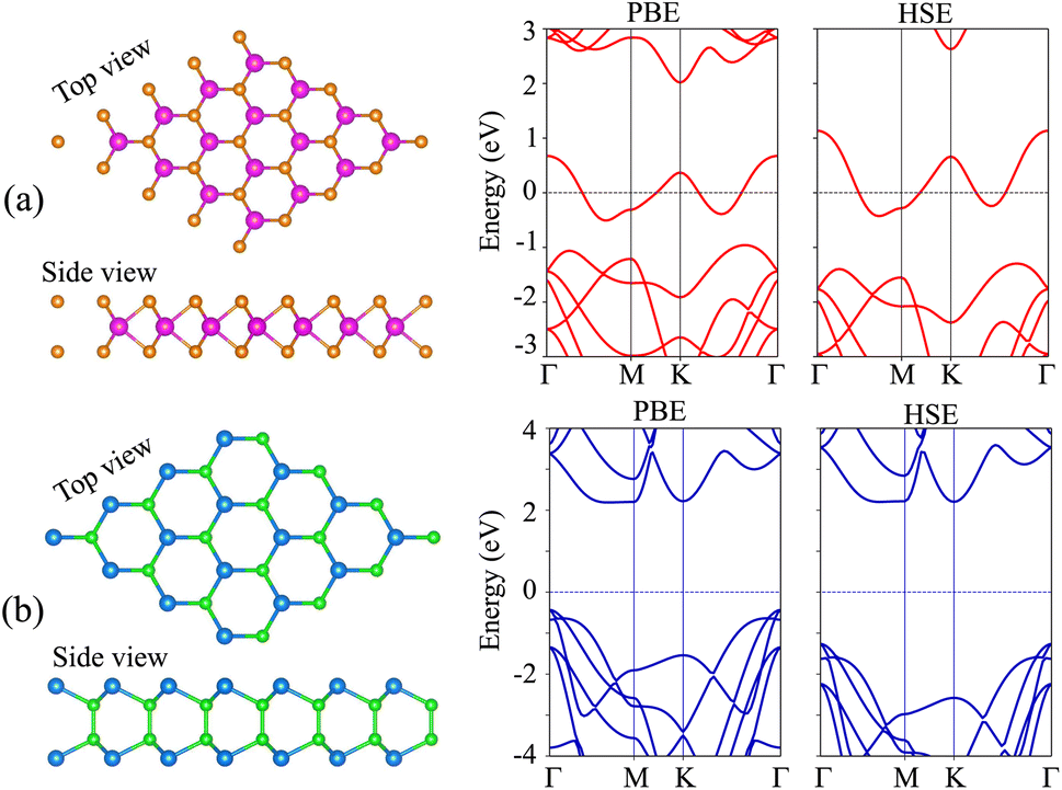
We first examine the atomic and electronic structures of NbS2 and BSe monolayers, as illustrated in Fig. 1. Both the NbS2 and BSe monolayers show hexagonal atomic crystals. In the NbS2 monolayer, one Nb atom is sandwiched between two S atoms on both sides, whereas in the BSe monolayer, each B atom is bonded with one Se atom on one side. The calculated lattice parameters of the NbS2 and BSe monolayers are 3.31 and 3.23 Å, respectively. These results are in good agreement with previous reports.50,61 The NbS2 monolayer is characterized by its metallic properties, featuring a band that crosses the Fermi level. In contrast, the BSe monolayer exhibits a semiconducting behavior with an indirect band gap of 2.62/3.46 eV, obtained by using the PBE/HSE functional. These values are in good agreement with previous measurements.50 The valence band maximum (VBM) and conduction band minimum (CBM) of the BSe monolayer are located at the Γ point and Γ–M path, respectively. Interestingly, we find that both the PBE and HSE functionals predict the similar behavior of NbS2 and BSe monolayers. The main difference between PBE and HSE methods is in a shift of the VBM of the BSe monolayer. The VBM of the BSe monolayer in the PBE functional is positioned closer to the Fermi level than that in the HSE functional.
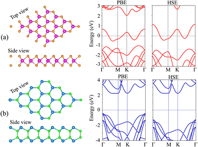 |
| | Fig. 1 (From left to right) Atomic structure, PBE and HSE band structures of (a) NbS2 and (b) BSe monolayers. Orange and purple balls represent the S and Nb atoms, respectively. Dark green and green balls stand for the Se and B atoms, respectively. | |
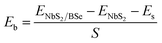
We now combine the NbS2 and BSe monolayers to generate the metal/semiconductor NbS2/BSe heterostructure by stacking NbS2 on top of the BSe monolayer. The possible stacking configurations of the NbS2/BSe heterostructure are depicted in Fig. 2. Due to a small difference in the lattice parameters between NbS2 and BSe monolayers, the NbS2/BSe heterostructure has a small lattice mismatch of only 1.2% for all stacking configurations. After the geometric optimization process, the interlayer spacing d between NbS2 and BSe layers in their heterostructure can be obtained, as listed in Table 1. It is evident that the interlayer spacing in the AC1 stacking configuration is d = 2.95 Å, which is the shortest among the eight stacking configurations. In addition, it should be noted that the interlayer spacing d in all stacking configurations is larger than the sum of covalent radii between S (0.99 Å) and Se (1.14 Å) atoms, confirming that there is no covalent bond between the two constituent NbS2 and BSe layers. Furthermore, to examine the interfacial stability of the NbS2/BSe heterostructure for all stacks, we calculate the binding energy as follows:
| |  | (1) |
Here,
ENbS2/BSe,
ENbS2 and
EBSe are the total energies of the NbS
2/BSe heterostructure, and isolated NbS
2 and BSe monolayers, respectively.
S = 10.69 Å
2 is the surface area of the heterostructure. The calculated
Eb for all stacks of the NbS
2/BSe heterostructure is listed in
Table 1. The binding energy of the NbS
2/BSe heterostructure is approximately averaged at about −20 meV Å
−2. The negative binding energy suggests that the NbS
2/BSe heterostructure is stable. Interestingly, this binding energy is comparable to that in graphite
62 and other typical 2D van der Waals (vdW) heterostructures.
63,64 This finding indicates that the NbS
2/BSe heterostructure can be synthesized in future experiments by different strategies, including mechanical exfoliation
12 and CVD.
65 For instance, using the CVD method, Fu
et al.37 successfully synthesized a metal/semiconductor NbS
2/MoS
2 heterostructure with high quality and a clean interface. Among these stacks, the AC2 stack has the lowest binding energy of −23.89 meV Å
−2. The shortest interlayer spacing and the lowest binding energy in the AC1 stacking configuration of the NbS
2/BSe heterostructure indicate that the AC1 stack is the most energetically feasible stacking configuration.
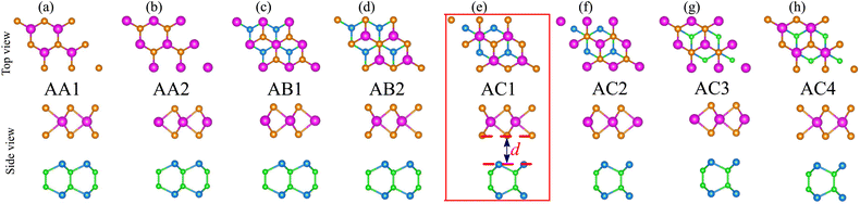 |
| | Fig. 2 Atomic structures of the NbS2/BSe heterostructure for possible different stacking configurations of (a) AA1, (b) AA2, (c) AB1, (d) AB2, (e) AC1, (f) AC2, (g) AC3 and (h) AC4. | |
Table 1 Calculated interlayer spacing (d, Å), binding energy (Eb, meV Å−2), and Schottky barrier heights (Φn and Φp, eV) of the NbS2/BSe heterostructure
| Stacks |
D
|
E
b
|
Φ
n
|
Φ
p
|
Contact types |
| AA1 |
3.11 |
−22.16 |
2.12 |
0.36 |
p-type ShC |
| AA2 |
3.58 |
−14.50 |
2.05 |
0.51 |
p-type ShC |
| AB1 |
2.95 |
−23.88 |
1.97 |
0.42 |
p-type ShC |
| AB2 |
3.01 |
−23.47 |
2.0 |
0.43 |
p-type ShC |
| AC1 |
2.95 |
−23.89 |
1.97 |
0.42 |
p-type ShC |
| AC2 |
3.01 |
−23.47 |
2.01 |
0.42 |
p-type ShC |
| AC3 |
3.58 |
−14.67 |
2.05 |
0.51 |
p-type ShC |
| AC4 |
3.04 |
−23.01 |
2.10 |
0.34 |
p-type ShC |
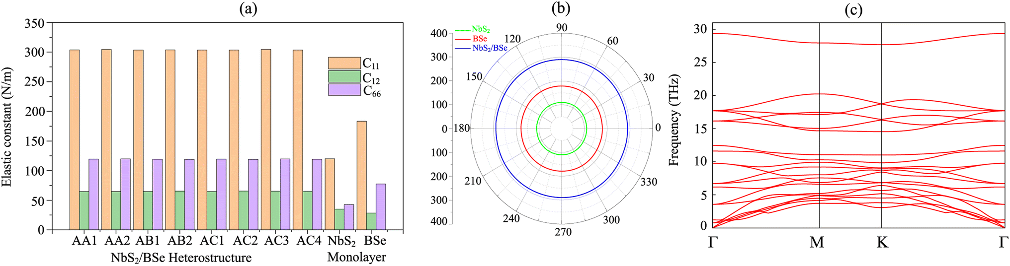
Furthermore, to check the mechanical stability of the NbS2/BSe heterostructure, we consider its independent elastic constants (Cij). The Cij of the perfect NbS2 and BSe monolayers are also calculated for comparison, as illustrated in Fig. 3. The calculated elastic constants C11, C12 and C66 of monolayers NbS2 and BSe are 183.31, 28.40, 77.45 and 120.10, 34.91 and 42.59 N m−1, respectively. According to the Born–Huang stability criteria,66i.e. C11 > C12, C66 > 0 and C112 – C122 > 0, both the NbS2 and BSe monolayers are mechanically stable. Interestingly, the formation of the NbS2/BSe heterostructure leads to an increase in the elastic constants Cij, as shown in Fig. 3(a). The calculated C11, C12 and C66 of the NbS2/BSe heterostructure are about 300, 65 and 130 N m−1, respectively. These values of the elastic constants are still larger than those of the NbS2 and BSe monolayers. In addition, the elastic constants of the NbS2/BSe heterostructure meet the Born–Huang stability criteria. This finding suggests that the NbS2/BSe heterostructure exhibits outstanding mechanical stability. Furthermore, the angle-dependent Young's modulus of NbS2 and BSe monolayers and their combined NbS2/BSe heterostructure for the most energetically favorable stacking configuration are depicted in Fig. 3(b). We find that the Young's modulus of the NbS2/BSe heterostructure is calculated to be 289.74 N m−1, which is greater than that of the NbS2 (109.95 N m−1) and BSe (178.90 N m−1) monolayers. The phonon dispersion curves of the NbS2/BSe heterostructure are depicted in Fig. 3(c). We observe that there are no imaginary frequencies in the phonon spectrum of the NbS2/BSe heterostructure, indicating that such a heterostructure is dynamically stable. All these findings indicate that the NbS2/BSe heterostructure can be considered as a promising candidate for the design of electronic devices.
 |
| | Fig. 3 (a) Calculated independent elastic constants (Cij) of the NbS2/BSe heterostructure for different stacking configurations and (b) angle-dependent Young's modulus and (c) phonon dispersion curves of the NbS2/BSe heterostructure for the most energetically favorable stacking configuration. | |
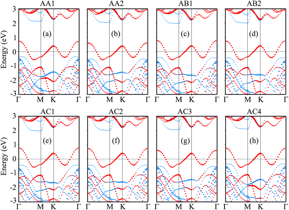
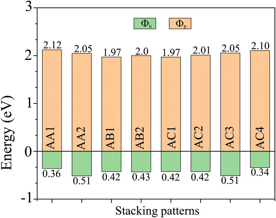
The projected band structures of the NbS2/BSe heterostructure for all stacks are depicted in Fig. 4, in which red and blue bubbles show the contributions of the NbS2 and BSe layers, respectively. It is obvious that the band structures of the NbS2/BSe heterostructure appear to be a combination of the band structures of the constituent monolayers. The reason for such a combination is weak interactions between the NbS2 and BSe layers. These weak interactions play a pivotal role in stabilizing the heterostructure, making it readily obtainable in experiments. Furthermore, the combination between the metallic NbS2 monolayer and semiconducting BSe monolayer might give rise to the formation of either a Schottky or ohmic contact, depending on the position of the band edges of the BSe semiconductor in relation to the Fermi level of the metallic NbS2 layer. As depicted in Fig. 4, the Fermi level of the metallic NbS2 monolayer lies between the band edges of the semiconductor BSe monolayer. This arrangement leads to the formation of a Schottky contact. In a Schottky contact, Schottky barriers exist, and these barriers can be determined as follows:
and
Here,
ECBM and
EVBM are the band edge energies of the CBM and VBM of the BSe semiconductor, respectively.
EF is the Fermi level of the heterostructure. The obtained Schottky barriers
Φn and
Φp of the heterostructure are listed in
Table 1 and
Fig. 5. It is evident that the Schottky barrier
Φp of the heterostructure is always narrower than the Schottky barrier
Φn, indicating that the NbS
2/BSe heterostructure tends to exhibit p-type ShC. The p-type Schottky barrier in the NbS
2/BSe heterostructure ranges from 0.34 to 0.51 eV. The AC4 stacking pattern exhibits the narrowest Schottky barrier
Φp of 0.34 eV, while the AA2 and AC3 stacking patterns exhibit the highest Schottky barrier
Φp of 0.51 eV. As previously discussed, the AC1 stacking pattern of the NbS
2/BSe heterostructure is the most favorable among the stacking configurations. Hence, we will focus on this stacking configuration in our subsequent calculations.
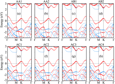 |
| | Fig. 4 Projected band structures of the NbS2/BSe heterostructure for different stacks of (a) AA1, (b) AA2, (c) AB1, (d) AB2, (e) AC1, (f) AC2, (g) AC3 and (h) AC4. Red and blue bubbles represent the contributions of the NbS2 and BSe layers, respectively. | |
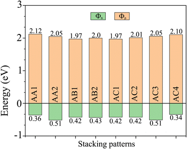 |
| | Fig. 5 The Schottky barriers of the NbS2/BSe heterostructure for different stacking patterns. | |
The projected band structures of the NbS2/BSe heterostructure for the most energetically favorable stacking patterns using PBE and HSE methods are illustrated in Fig. 6(a). The calculated Schottky barriers Φn and Φp of the NbS2/BSe heterostructure are 1.97/2.88 and 0.42/0.43 eV, obtained using the PBE/HSE functional. It is clear that both the PBE and HSE functionals predict the similar behavior of the NbS2/BSe heterostructure. The CBM calculated using the HSE functional of the NbS2/BSe heterostructure is positioned further away from the Fermi level than that calculated by using the PBE functional. Interestingly, it's worth noting that both the PBE and HSE functional predictions indicate a p-type Schottky contact with the same Schottky barrier Φp. This suggests that the PBE functional can be effectively used in the subsequent calculations without compromising the accuracy of the results. Furthermore, in order to verify the thermal stability of the NbS2/BSe heterostructure, we perform ab initio molecular dynamics (AIMD) simulation. The AIMD simulation of the NbS2/BSe heterostructure is displayed in Fig. 6(b). It is evident that the fluctuation in the total energy of the NbS2/BSe heterostructure as a function of time steps is small. In addition, the atomic structure of the NbS2/BSe heterostructure after heating for 5 ps is preserved without any distortion. All these findings confirm that the NbS2/BSe heterostructure is thermally stable. The stability indicates that the NbS2/BSe heterostructure could be synthesized and used in recent nanoelectronic and optoelectronic devices, such as Schottky diodes, field-effect transistors and photodetectors.
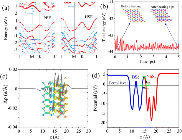 |
| | Fig. 6 (a) Projected band structures, (b) AIMD simulation, (c) charge density difference and (d) electrostatic potential of the AC1 stacking pattern of the NbS2/BSe heterostructure. Red and blue lines represent the contribution of metallic NbS2 and semiconducting BSe monolayers, respectively. The inset of (c) shows the atomic structure of the heterostructure before and after heating for 5 ps. Yellow and cyan regions in (c) indicate the charge accumulation and depletion, respectively. | |
Furthermore, the charge transfers between the NbS2 and BSe layers in their heterostructure are also explored by calculating the charge density difference (CDD) as follows:
| | | Δρ = ρNbS2/BSe − ρNbS2 − ρBSe | (4) |
Here, the charge densities of the NbS
2/BSe heterostructure and isolated NbS
2 and BSe monolayers are denoted as
ρNbS2/BSe,
ρNbS2 and
ρBSe, respectively. The CDD of the NbS
2/BSe heterostructure is depicted in
Fig. 6(c). One can find that the charges are accumulated mainly around the NbS
2 layer and depleted mainly around the BSe layer. This finding implies that the electrons are transferred from the NbS
2 to the BSe layer in their corresponding NbS
2/BSe heterostructure. Based on Bader charge analysis, there is a small amount of charge transfer of only 0.02 electrons that flow from the NbS
2 to the BSe layer.
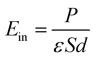
The electrostatic potential of the NbS2/BSe heterostructure is depicted in Fig. 6(d). One can observe that the NbS2 layer has a deeper potential that the BSe layer in their heterostructure. The charge transfer between metallic NbS2 and BSe layers at the interface of the NbS2/BSe heterostructure gives rise to the formation of an interfacial dipole, which can be obtained using ΔV = WNbS2 − WNbS2/BSe, where the work functions of the metallic NbS2 layer and the NbS2/BSe heterostructure are denoted as the WNbS2 and WNbS2/BSe, respectively. The interfacial dipole at the interface of the NbS2/BSe heterostructure is obtained to be 0.02 eV. The formation of the interfacial dipole at the interface can change the Schottky barriers. However, our results show that both the amount of charge transfer and interface dipole are small; hence, the change in the Schottky barriers at the interface of the NbS2/BSe heterostructure can be considered negligible. Furthermore, both the charge transfer and interfacial dipole in the NbS2/BSe heterostructure may give rise to the formation of a built-in electric field at the interface. The built-in electric field can be calculated as follows:67
| |  | (5) |
where
P stands for the interface dipole.
ε,
S and
d are the dielectric constant, surface area and interlayer distance of the NbS
2/BSe heterostructure, respectively. We can observe that the built-in electric field is directly proportional to the interface dipole. As we have discussed above, the amount of charge transfer and interface dipole of the NbS
2/BSe heterostructure are small; hence, the built-in electric field across the interface of the heterostructure is also small and can be considered negligible.
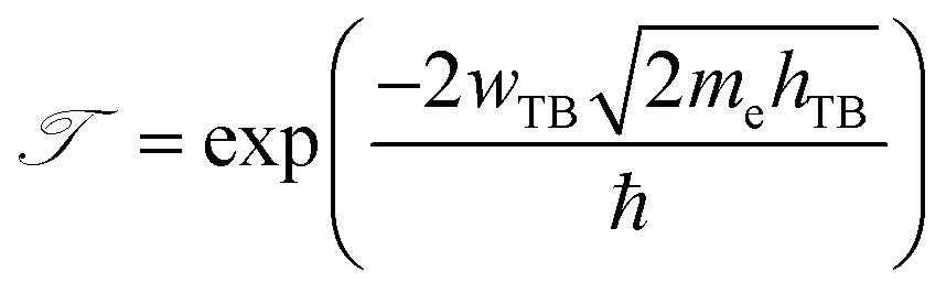
Furthermore, in order to evaluate the efficiency of electron injection through the contact of the NbS2/MoSSe heterostructure, we add the calculations on the tunneling probability  and the tunneling-specific resistivity (ρt) as follows:
| | 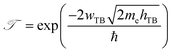 | (6) |
and
| | 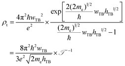 | (7) |
Here, ℏ is the reduced Planck's constant.
e and
me are the electron magnitude and mass of a free electron, respectively.
hTB and
wTB are the tunneling barrier height and width, respectively, which can be obtained directly from the electrostatic potential of the NbS
2/BSe heterostructure. The calculated
hTB and
wTB of the NbS
2/BSe heterostructure for the most energetically favorable stacking configuration are 3.68 eV and 1.35 Å, respectively. Hence, the tunneling probability and contact tunneling-specific resistivity at the interface of the NbS
2/BSe heterostructure are about 7% and 2.09 × 10
−10 Ω cm
2, respectively. We also observe that the value of the tunneling-specific resistivity at the interface of the NbS
2/MoSSe heterostructure exhibits a magnitude similar to that in other metal/semiconductor contacts, such as Bi/MoS
2,
68 semimetals/TMDs,
69 metal/MSi
2N
4 (M = Mo, W)
29 and 2D (3D) metals/GeSe.
70 This finding also suggests that the NbS
2/BSe heterostructure could serve as an efficient contact for electronic devices.
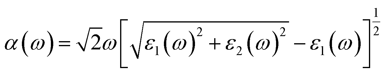
Furthermore, we calculate the optical absorption of the NbS2/BSe heterostructure as well as that of the constituent NbS2 and BSe monolayers for comparison. The optical absorption can be obtained as follows:
| |  | (8) |
Here, the real and imaginary parts of dielectric functions are denoted ass
ε1 and
ε2, respectively. The optical absorption of the NbS
2/BSe heterostructure and the constituent NbS
2 and BSe monolayers are depicted in
Fig. 7. We can find that the optical absorption coefficient of the NbS
2/BSe heterostructure can reach up to 5 × 10
5 cm
−1 at a photon energy of about 5 eV, which is still greater than that in the constituent NbS
2 and BSe monolayers. Hence, the formation of the M–S NbS
2/BSe heterostructure gives rise to an enhancement in the optical absorption of both NbS
2 and BSe monolayers. The enhancement in the optical absorption of the M–S NbS
2/BSe heterostructure indicates that it can be considered as a promising candidate for the design of optoelectronic devices.
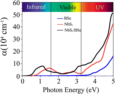 |
| | Fig. 7 Calculated optical absorption as a function of the photon energy of the NbS2/BSe heterostructure and the constituent BSe and NbS2 monolayers. | |
4 Conclusions
In summary, we have designed a metal/semiconductor heterostructure between two different materials 2D NbS2 metal and 2D BSe semiconductor using first-principles prediction. The combination between NbS2 and BSe monolayers gives rise to the formation of a metal/semiconductor NbS2/BSe heterostructure with different stacking configurations. All these stacking configurations of the NbS2/BSe heterostructure are considered to be structurally, mechanically and thermally stable, suggesting their potential as components in electronic devices. The formation of the NbS2/BSe heterostructure leads to the generation of a Schottky contact with the Schottky barrier ranging from 0.36 to 0.51 eV, depending on the stacking configurations. In addition, the optical absorption coefficient of the NbS2/BSe heterostructure can reach up to 5 × 105 cm−1 at a photon energy of about 5 eV, which is still greater than that in the constituent NbS2 and BSe monolayers. This finding suggests that the formation of the M–S NbS2/BSe heterostructure gives rise to an enhancement in the optical absorption of both NbS2 and BSe monolayers. Notably, the tunneling probability and the contact tunneling-specific resistivity at the interface of the NbS2/BSe heterostructure are low, indicating its applicability in emerging nanoelectronic and optoelectronic devices, such as Schottky diodes, field-effect transistors and photodetectors. Our findings offer valuable insights for the practical utilization of electronic and optoelectronic devices based on the NbS2/BSe heterostructure.
Conflicts of interest
There are no conflicts to declare.
Acknowledgements
This research is funded by Ministry of Education and Training of Vietnam under grant number B2022-TNA-36 and is partially funded by the TNU-University of Sciences under the project code: CS2023-TN06-09.
References
- K. S. Novoselov, A. K. Geim, S. V. Morozov, D.-e. Jiang, Y. Zhang, S. V. Dubonos, I. V. Grigorieva and A. A. Firsov, Science, 2004, 306, 666–669 CrossRef CAS PubMed.
- A. Carvalho, M. Wang, X. Zhu, A. S. Rodin, H. Su and A. H. Castro Neto, Nat. Rev. Mater., 2016, 1, 1–16 Search PubMed.
- S. Manzeli, D. Ovchinnikov, D. Pasquier, O. V. Yazyev and A. Kis, Nat. Rev. Mater., 2017, 2, 1–15 Search PubMed.
- Y. Wu, K. A. Jenkins, A. Valdes-Garcia, D. B. Farmer, Y. Zhu, A. A. Bol, C. Dimitrakopoulos, W. Zhu, F. Xia and P. Avouris,
et al.
, Nano Lett., 2012, 12, 3062–3067 CrossRef CAS PubMed.
- H. Chang and H. Wu, Adv. Funct. Mater., 2013, 23, 1984–1997 CrossRef CAS.
- W. Han, R. K. Kawakami, M. Gmitra and J. Fabian, Nat. Nanotechnol., 2014, 9, 794–807 CrossRef CAS PubMed.
- T. Wehling, K. Novoselov, S. Morozov, E. Vdovin, M. Katsnelson, A. Geim and A. Lichtenstein, Nano Lett., 2008, 8, 173–177 CrossRef CAS PubMed.
- T. Kuila, S. Bose, A. K. Mishra, P. Khanra, N. H. Kim and J. H. Lee, Prog. Mater. Sci., 2012, 57, 1061–1105 CrossRef CAS.
- G. Gui, J. Li and J. Zhong, Phys. Rev. B: Condens. Matter Mater. Phys., 2008, 78, 075435 CrossRef.
- M. Y. Han, B. Özyilmaz, Y. Zhang and P. Kim, Phys. Rev. Lett., 2007, 98, 206805 CrossRef PubMed.
- Y. Liu, N. O. Weiss, X. Duan, H.-C. Cheng, Y. Huang and X. Duan, Nat. Rev. Mater., 2016, 1, 1–17 Search PubMed.
- A. Castellanos-Gomez, X. Duan, Z. Fei, H. R. Gutierrez, Y. Huang, X. Huang, J. Quereda, Q. Qian, E. Sutter and P. Sutter, Nat. Rev. Methods Primers, 2022, 2, 58 CrossRef CAS.
- L. Samad, S. M. Bladow, Q. Ding, J. Zhuo, R. M. Jacobberger, M. S. Arnold and S. Jin, ACS Nano, 2016, 10, 7039–7046 CrossRef CAS PubMed.
- K. Novoselov, A. Mishchenko, A. Carvalho and A. Castro Neto, Science, 2016, 353, aac9439 CrossRef CAS PubMed.
- Z. Guo, L. Wang, M. Han, E. Zhao, L. Zhu, W. Guo, J. Tan, B. Liu, X.-Q. Chen and J. Lin, ACS Nano, 2022, 16, 11268–11277 CrossRef CAS PubMed.
- Y. Gong, S. Lei, G. Ye, B. Li, Y. He, K. Keyshar, X. Zhang, Q. Wang, J. Lou and Z. Liu,
et al.
, Nano Lett., 2015, 15, 6135–6141 CrossRef CAS PubMed.
- Y. Luo, K. Ren, S. Wang, J.-P. Chou, J. Yu, Z. Sun and M. Sun, J. Phys. Chem. C, 2019, 123, 22742–22751 CrossRef CAS.
- Y. Wang, R. Chen, X. Luo, Q. Liang, Y. Wang and Q. Xie, ACS Appl. Nano Mater., 2022, 5, 8371–8381 CrossRef CAS.
- Z. Ben Aziza, H. Henck, D. Pierucci, M. G. Silly, E. Lhuillier, G. Patriarche, F. Sirotti, M. Eddrief and A. Ouerghi, ACS Nano, 2016, 10, 9679–9686 CrossRef CAS PubMed.
- C.-J. Shih, Q. H. Wang, Y. Son, Z. Jin, D. Blankschtein and M. S. Strano, ACS Nano, 2014, 8, 5790–5798 CrossRef CAS PubMed.
- B. Marfoua and J. Hong, Adv. Mater. Interfaces, 2023, 10, 2202387 CrossRef CAS.
- B. Zhao, R. Ngaloy, S. Ghosh, S. Ershadrad, R. Gupta, K. Ali, A. M. Hoque, B. Karpiak, D. Khokhriakov and C. Polley,
et al.
, Adv. Mater., 2023, 35, 2209113 CrossRef CAS PubMed.
- C. K. Borah, P. K. Tyagi and S. Kumar, Nanoscale Adv., 2020, 2, 3231–3243 RSC.
- W. Yu, Z. Zhu, S. Zhang, X. Cai, X. Wang, C.-Y. Niu and W.-B. Zhang, Appl. Phys. Lett., 2016, 109, 103104 CrossRef.
- Y. Zheng, Y. Chen, B. Gao, B. Lin and X. Wang, Engineering, 2021, 7, 991–1001 CrossRef CAS.
- J. E. Padilha, A. Fazzio and A. J. da Silva, Phys. Rev. Lett., 2015, 114, 066803 CrossRef CAS PubMed.
- C. C. Tho, S.-D. Guo, S.-J. Liang, W. L. Ong, C. S. Lau, L. Cao, G. Wang and Y. S. Ang, Appl. Phys. Rev., 2023, 10, 041307 CAS.
- Y. Yin, Q. Gong, M. Yi and W. Guo, Adv. Funct. Mater., 2023, 33, 2214050 CrossRef CAS.
- C. C. Tho, C. Yu, Q. Tang, Q. Wang, T. Su, Z. Feng, Q. Wu, C. Nguyen, W.-L. Ong and S.-J. Liang,
et al.
, Adv. Mater. Interfaces, 2023, 10, 2201856 CrossRef CAS.
- Q. Wang, L. Cao, S.-J. Liang, W. Wu, G. Wang, C. H. Lee, W. L. Ong, H. Y. Yang, L. K. Ang and S. A. Yang,
et al.
, npj 2D Mater. Appl., 2021, 5, 71 CrossRef CAS.
- J. Su, L. Feng, Y. Zhang and Z. Liu, Phys. Chem. Chem. Phys., 2016, 18, 16882–16889 RSC.
- W. Xiong, C. Xia, X. Zhao, T. Wang and Y. Jia, Carbon, 2016, 109, 737–746 CrossRef CAS.
- D. Zhang, Y. Hu, H. Zhong, S. Yuan and C. Liu, Nanoscale, 2019, 11, 13800–13806 RSC.
- Q. Luo, S. Yin, X. Sun, G. Guo and X. Dai, Diamond Relat. Mater., 2022, 128, 109223 CrossRef CAS.
- S. Wang, J.-P. Chou, C. Ren, H. Tian, J. Yu, C. Sun, Y. Xu and M. Sun, Sci. Rep., 2019, 9, 5208 CrossRef PubMed.
- M. Sun, J.-P. Chou, Q. Ren, Y. Zhao, J. Yu and W. Tang, Appl. Phys. Lett., 2017, 110, 173105 CrossRef.
- Q. Fu, X. Wang, J. Zhou, J. Xia, Q. Zeng, D. Lv, C. Zhu, X. Wang, Y. Shen and X. Li,
et al.
, Chem. Mater., 2018, 30, 4001–4007 CrossRef CAS.
- X. Ding, S. Zhang, M. Zhao, Y. Xiang, K. H. Zhang, X. Zu, S. Li and L. Qiao, Phys. Rev. Appl., 2019, 12, 064061 CrossRef CAS.
- B. Wang, H. Luo, X. Wang, E. Wang, Y. Sun, Y.-C. Tsai, H. Zhu, P. Liu, K. Jiang and K. Liu, ACS Nano, 2019, 14, 175–184 CrossRef PubMed.
- Z. Golsanamlou, P. Kumari, L. Sementa, T. Cusati, G. Iannaccone and A. Fortunelli, Adv. Electron. Mater., 2022, 8, 2200020 CrossRef CAS.
- S. Zhao, T. Hotta, T. Koretsune, K. Watanabe, T. Taniguchi, K. Sugawara, T. Takahashi, H. Shinohara and R. Kitaura, 2D Mater., 2016, 3, 025027 CrossRef.
- Z. Wang, C.-Y. Cheon, M. Tripathi, G. M. Marega, Y. Zhao, H. G. Ji, M. Macha, A. Radenovic and A. Kis, ACS Nano, 2021, 15, 18403–18410 CrossRef CAS PubMed.
- Z. Zhang, P. Yang, M. Hong, S. Jiang, G. Zhao, J. Shi, Q. Xie and Y. Zhang, Nanotechnology, 2019, 30, 182002 CrossRef CAS PubMed.
- J. J. Ni, L. Yang and H. X. Yang, Mater. Today Commun., 2022, 33, 104720 CrossRef CAS.
- V. Kumar, S. Khandelwal, A. Khuraijam and N. Halder, Mater. Today: Proc., 2022, 62, 1580–1584 CAS.
- S. Mankovsky, S. Polesya, H. Ebert and W. Bensch, Phys. Rev. B, 2016, 94, 184430 CrossRef.
- Y. Kim, K. C. Kwon, S. Kang, C. Kim, T. H. Kim, S.-P. Hong, S. Y. Park, J. M. Suh, M.-J. Choi and S. Han,
et al.
, ACS Sens., 2019, 4, 2395–2402 CrossRef CAS PubMed.
- T. Li, Q. Miao, Y. Wang and H. Yang, Surf. Interfaces, 2023, 42, 103336 CrossRef CAS.
- J. Zhou, Y. Shen, F. Lv, W. Zhang, F. Lin, W. Zhang, K. Wang, H. Luo, Q. Wang and H. Yang,
et al.
, Adv. Funct. Mater., 2022, 32, 2204495 CrossRef CAS.
- S. Demirci, N. Avazlı, E. Durgun and S. Cahangirov, Phys. Rev. B: Condens. Matter Mater. Phys., 2017, 95, 115409 CrossRef.
- S.-T. Nguyen, C. Q. Nguyen, Y. S. Ang, N. Van Hoang, N. M. Hung and C. V. Nguyen, Langmuir, 2023, 39, 6637–6645 CrossRef CAS PubMed.
- B.-J. Wang, X.-H. Li, R. Zhao, X.-L. Cai, W.-Y. Yu, W.-B. Li, Z.-S. Liu, L.-W. Zhang and S.-H. Ke, J. Mater. Chem. A, 2018, 6, 8923–8929 RSC.
- D. Zhang, Q. Gao, Y. Chen, Y. Xia, H. Wang, H. Wang and Y. Ni, Adv. Theory Simul., 2020, 3, 2000144 CrossRef CAS.
- K. Ren, J. Yu and W. Tang, J. Alloys Compd., 2020, 812, 152049 CrossRef CAS.
- P. Giannozzi, S. Baroni, N. Bonini, M. Calandra, R. Car, C. Cavazzoni, D. Ceresoli, G. L. Chiarotti, M. Cococcioni and I. Dabo,
et al.
, J. Phys.: Condens. Matter, 2009, 21, 395502 CrossRef PubMed.
- J. P. Perdew, K. Burke and M. Ernzerhof, Phys. Rev. Lett., 1996, 77, 3865 CrossRef CAS PubMed.
- J. P. Perdew, K. Burke and M. Ernzerhof, Phys. Rev. Lett., 1998, 80, 891 CrossRef CAS.
- G. Kresse and D. Joubert, Phys. Rev. B: Condens. Matter Mater. Phys., 1999, 59, 1758 CrossRef CAS.
- S. Grimme, J. Comput. Chem., 2006, 27, 1787–1799 CrossRef CAS PubMed.
- J. Heyd and G. E. Scuseria, J. Chem. Phys., 2004, 121, 1187–1192 CrossRef CAS PubMed.
- K. Ren, Y. Luo, S. Wang, J.-P. Chou, J. Yu, W. Tang and M. Sun, ACS Omega, 2019, 4, 21689–21697 CrossRef CAS PubMed.
- S. D. Chakarova-Käck, E. Schröder, B. I. Lundqvist and D. C. Langreth, Phys. Rev. Lett., 2006, 96, 146107 CrossRef PubMed.
- H. Saini, M. Jyothirmai, U. V. Waghmare and R. Thapa, Phys. Chem. Chem. Phys., 2020, 22, 2775–2782 RSC.
- T. Björkman, A. Gulans, A. V. Krasheninnikov and R. M. Nieminen, Phys. Rev. Lett., 2012, 108, 235502 CrossRef PubMed.
- X. Zhou, X. Hu, J. Yu, S. Liu, Z. Shu, Q. Zhang, H. Li, Y. Ma, H. Xu and T. Zhai, Adv. Funct. Mater., 2018, 28, 1706587 CrossRef.
- F. Mouhat and F.-X. Coudert, Phys. Rev. B: Condens. Matter Mater. Phys., 2014, 90, 224104 CrossRef.
- X. Li, Z. Li and J. Yang, Phys. Rev. Lett., 2014, 112, 018301 CrossRef PubMed.
- P.-C. Shen, C. Su, Y. Lin, A.-S. Chou, C.-C. Cheng, J.-H. Park, M.-H. Chiu, A.-Y. Lu, H.-L. Tang and M. M. Tavakoli,
et al.
, Nature, 2021, 593, 211–217 CrossRef CAS PubMed.
- T. Su, Y. Li, Q. Wang, W. Zhao, L. Cao and Y. S. Ang, J. Phys. D: Appl. Phys., 2023, 56, 234001 CrossRef.
- L. Cao, X. Deng, Z. Tang, G. Zhou and Y. S. Ang, Appl. Phys. Lett., 2022, 121, 113104 CrossRef CAS.
|
| This journal is © The Royal Society of Chemistry 2024 |
Click here to see how this site uses Cookies. View our privacy policy here. 
 Open Access Article
 This Open Access Article is licensed under a
  bc,
N. X.
Ca
bc,
N. X.
Ca


 and the tunneling-specific resistivity (ρt) as follows: