
 Open Access Article
 This Open Access Article is licensed under a Creative Commons Attribution-Non Commercial 3.0 Unported Licence
Electronic, magnetic, and optical properties of Np and Pu decorated armchair graphene nanoribbons: a DFT study
Nguyen Thi
Han
 *a,
K. Dien
Vo
bc,
Tu
Le Manh
a,
Ong Kim
Le
de and
Dinh Thuy
Van
f
*a,
K. Dien
Vo
bc,
Tu
Le Manh
a,
Ong Kim
Le
de and
Dinh Thuy
Van
f
aFaculty of Materials Science and Engineering, Phenikaa University, Yen Nghia, Ha Dong, Hanoi 12116, Vietnam. E-mail: han.nguyenthi@phenikaa-uni.edu.vn
bDivision of Applied Physics, Dong Nai Technology University, Bien Hoa City, Vietnam
cFaculty of Engineering, Dong Nai Technology University, Bien Hoa City, Vietnam
dInstitute of Fundamental and Applied Sciences, Duy Tan University, Ho Chi Minh City 70000, Vietnam
eFaculty of Natural Sciences, Duy Tan University, Da Nang City 50000, Vietnam
fFaculty of Chemistry, Thai Nguyen University of Education, 20 Luong Ngoc Quyen, Quang Trung, Thai Nguyen City, Vietnam
First published on 18th June 2024
Abstract
We employed Density Functional Theory (DFT) to investigate the electronic, magnetic, and optical characteristics of armchair graphene nanoribbons (AGNRs) decorated with neptunium (Np) and plutonium (Pu). Our analysis delves deeply into the intricate orbital hybridizations associated with C–Np, C–Pu, C–C, Np–Np, and Pu–Pu chemical bonds. Through this approach, we explore the electronic band structure, band-decomposed charge densities, spin–charge distributions, and Van Hove singularities in the density of states. Furthermore, our examination successfully correlates optical excitation with electronic band energy. Our results indicated that these rare-earth atoms are strongly bound to the edge structure of AGNRs, significantly altering their electronic, magnetic, and optical properties. Theoretical exploration not only reveals the intriguing physical and chemical properties of rare-earth (Np/Pu) decorated AGNRs but also presents a practical pathway for synthesizing novel materials.
1 Introduction
In 2004, a pivotal achievement occurred with the successful fabrication of graphene via the mechanical exfoliation method by Geim et al.1 Graphene represents the pioneering example of a truly two-dimensional (2D) material, poised to serve as an optimal platform for unlocking low-dimensional physics and applications.2 Graphene exhibits a distinctive property as a gapless semiconductor,3 characterized by a cone-like energy spectrum in proximity to the Fermi energy. The electronic properties of graphene give rise to numerous remarkable characteristics, such as high carrier mobility at 300 K (>200![[thin space (1/6-em)]](https://www.rsc.org/images/entities/char_2009.gif) 000 cm2 V−1 s−1),4 superior thermo-conductivity (3000–5000 W m−1 K−1),5 extremely high modulus (∼11 TPa)6 and tensile strength (∼1100 GPa),7 high transparency to incident light over a broad range of wavelengths (97.7%),8 and an anomalous quantum Hall effect.9 Since then, much research on graphene and other 2D graphene-like materials10–20 has captured the attention of experimental and theoretical researchers, spanning the realms of fundamental science and applied technology.21
000 cm2 V−1 s−1),4 superior thermo-conductivity (3000–5000 W m−1 K−1),5 extremely high modulus (∼11 TPa)6 and tensile strength (∼1100 GPa),7 high transparency to incident light over a broad range of wavelengths (97.7%),8 and an anomalous quantum Hall effect.9 Since then, much research on graphene and other 2D graphene-like materials10–20 has captured the attention of experimental and theoretical researchers, spanning the realms of fundamental science and applied technology.21
Particularly, considerable research interest has centered on one-dimensional (1D) graphene nanoribbons (GNRs), primarily due to their distinctive honeycomb lattice structure and the intriguing effects of finite-size quantum confinement.22 The creation of GNRs has been accomplished through various methodologies, with the most prevalent approaches involving the division of graphene via metal-catalyzed cutting processes,23 lithographic patterning,24 and plasma etching.25 To meet the demands of large-scale production essential for the semiconductor industry, the chemical vapor deposition technique has been refined for the synthesis of GNRs.26
Controlling the electronic, magnetic, and optical properties of GNRs is crucial for enhancing the efficiency of electronic and optical devices. The manipulation is achieved through multifaceted strategies such as edge modifications,27 surface adsorption,28 internal doping,29 and the strategic introduction of topological defects.30 Especially, within the variety of techniques, edge modification emerges as a prominent chemical methodology, yielding pronounced and controllable alterations in electromagnetic characteristics.
In the absence of passivation, pristine GNRs exhibit a planar structure characterized by open edges, which creates a chemically reactive environment.31 The presence of dangling bonds at the edges of carbon atoms renders them highly unstable, leading to the adsorption of atoms, molecules, or radical groups. These interactions induce substantial changes in both the fundamental electronic properties and the geometric arrangements of GNRs. The specific type and concentration of adsorbed adatoms play a pivotal role in governing the extent of these transformations. Theoretical calculations have indicated the stability of certain adatom-terminated GNR configurations, extending beyond the conventional H-terminated setups, for instance, K, F, O, B, Mg, Ru, and Te, as well as transition-metal-terminated GNRs.31–33 These insights illuminate the interplay between chemical modifications and the resultant modifications in the electronic and geometric characteristics of GNRs, offering a promising avenue for tailoring their properties to specific device applications.
In this study, we employ an advanced first-principles investigation based on DFT to comprehensively analyze the intricate electronic, magnetic, and optical attributes of Np and Pu decorated armchair graphene nanoribbons (AGNRs). We also established a similar calculation for the intrinsic and hydrogen-terminated armchair graphene nanoribbons (H-AGNRs) for comparison. Through methodical modifications, we systematically dissect and elucidate the pivotal contributions of these passivating species to a spectrum of essential properties. Our analysis is characterized by a coherent and meticulous approach, yielding consistent and robust observations. Consequently, we establish a comprehensive and unified understanding of the intricate interplay encompassing orbital hybridizations, spin configurations, electronic properties, and optical transitions. This study contributes to a deeper insight into the underlying principles governing nanoribbon behavior within well-defined theoretical frameworks.
2 Computational details
Density functional theory (DFT) calculations using the Vienna ab initio simulation package (VASP) and the Perdew–Burke–Ernzerhof (PBE) functional34,35 were performed to investigate the geometric and electronic properties of edge-adsorbed AGNRs. The projector-augmented wave pseudopotentials36 were used to capture electron and ion interactions. The functional PBE is known to generally underestimate dispersive interactions. To accurately determine system energy, the dispersion correction method is recommended.37 However, when it comes to electronic properties such as band structures and band gaps, the impact of dispersive corrections is minimal. Therefore, we have chosen not to incorporate the dispersion correction in our work. The wave functions are built from the plane waves with a maximum energy cutoff of 500 eV. The first Brillouin zone is sampled along the one-dimensional periodic direction by 22 × 1 × 1 and 100 × 1 × 1 k points in a Gamma scheme for structure relaxation and electronic properties, respectively. The convergence criterion for one full relaxation is determined by setting the Hellmann–Feynman forces to less than 0.01 eV Å−1, and the total energy difference to less than 10−6 eV.Additionally, this study uses the Hubbard-U method38 to address the computational shortcomings encountered in GGA calculations. The implementation of GGA + U (with U = 4.5) has been chosen to rectify the inadequate description of strongly localized electrons in the Np 5f and 6d/Pu 5f states.
3 Results and discussion
Armchair graphene nanoribbons (AGNRs) are excellent candidates for exhibiting diverse crystal phases following edge decorations. In this study, we focus on AGNRs with Na = 8 for modeling purposes. The process of creating edge terminated AGNRs involves two steps: first, generating AGNRs without edge passivation, and then introducing guest adatoms to passivate the dangling bonds. Each step was carefully optimized. After optimization, it was observed that AGNRs maintain their planar honeycomb structures even after the adsorption of adatoms (H/Np/Pu). The stability of these configurations can be evaluated based on their low binding energies. For a pristine system (Fig. 1a) because the ribbon edge is not terminated with adatoms, geometric reconstruction takes place, leading to the edge dangling bonds with non-uniform environments. Particularly, the outermost C–C lengths of 1.23 Å are much shorter than those of the ribbon center (1.43 Å). The edge structures are different before and after the chemical decorations. The H-AGNRs possess the well-known hexagonal plane (Fig. 1b), in which a tiny charge of about +0.01 e is transferred from C towards the H atoms. The rather strong chemical bonding with a bond length of 1.08 Å indicates the covalent nature of the C–H bond. This result is in good agreement with previous theoretical predictions.31 For rare-earth atoms, typical as Np/Pu, AGNRs present a non-uniform pentagon that appears in an armchair edge (Fig. 1c and d). Indeed, Np and Pu, characterized by their highly localized d and f orbitals, exhibit strong interactions with carbon atoms, with the Np–Np/Pu–Pu and C–Np/C–Pu bond lengths listed in Table 1, respectively. According to Bader charge analysis, a large amount of charge transfers from the Np/Pu toward C. Furthermore, the non-uniform C–C bond lengths are reduced to 1.39–1.43 Å. These reflect more stable structures due to the edge passivation. | ||
| Fig. 1 The optimal one-dimensional (1D) crystal structures for (a) AGNRs [Na = 8], (b) H-AGNRs, (c) Np-AGNRs, and (d) Pu-AGNRs. | ||
| Adatom | dC−X (Å) | d C−C (Å) | μ B | CT (e) | E i/dg/M (eV) |
|---|---|---|---|---|---|
| None | — | 1.24 | 0.00 | — | E ig = 0.43 |
| H | 1.08 | 1.37 | 0.00 | +0.01 | E dg = 0.42 |
| Np | 2.41 | 1.39 | 4.23 | −1.97 | M |
| Pu | 2.39 | 1.39 | 5.43 | −1.90 | M |
Shown in Fig. 2a–d are the charge density distributions of the studied materials, suggesting highly non-uniform environments of the chemical bonds, in which they directly reflect chemical bonding strength. All the C–C bonds possess strong covalent σ bonds and relatively weak π bonds simultaneously. Such bonds are enhanced for the edge C–C bonds in pristine systems, as shown by the dark red region in Fig. 2a. This is responsible for the shortened bond lengths and the energy range of edge-atom-dominated bands. As for H-terminated ones, the C–H bonds are revealed by the red region between them, while the edge C–C bonds are weakened under the loss of the σ electrons (Fig. 2b). The above similar behaviors are also true for the case of rare-earth decorations (Fig. 2c and d); the saturated guest–host bonds can create very rich multi-orbital hybridizations and strong deformation of the nearest and even second nearest-neighbor C–C bonds. In addition, the atomic interactions, which are associated with the edge-dependent closed pentagon, present an expansion, and a weak but important charge density redistribution occurred at the edge C–Pu. This phenomenon clearly illustrates the metallic nature of this chemical bonding.
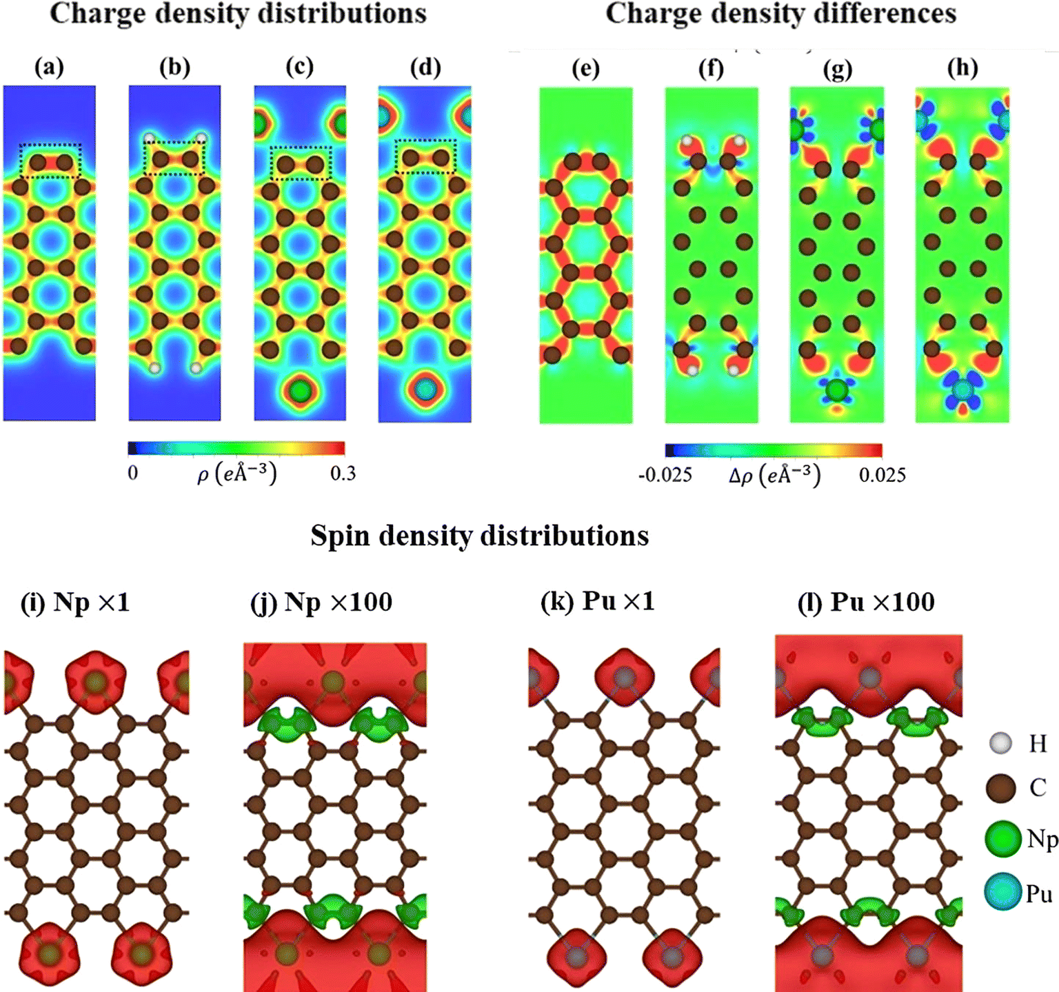 | ||
| Fig. 2 (a)–(d) The charge density distributions of pure AGNRs, H-AGNRs, Np-AGNRs, and Pu-AGNRs, the corresponding charge density difference, respectively (e)–(h). The spin density distribution and it's the corresponding enlarged pictures for (i)–(l) Np-AGNRs, and Pu-AGNRs. The red iso-surface indicates the spin-up component, while the green part denotes the spin-down charge density. | ||
The charge density difference can provide more useful information about the atomic interactions and reveal a concise critical picture of the orbital hybridizations. This could be achieved by the subtraction of the isolated atoms from that of the armchair nanoribbons. As for pristine ribbons in Fig. 2e, the strong σ bonding is exhibited by the charge distribution between two carbon atoms. There are more charges distributed at the ribbon edge indicating the triple nature. Variation of charge in H-AGNRs illustrates the clear image of charge transfer from edge carbons to hydrogens (Fig. 2f). This accounts for the vanishing of the edge-atom dominated energy band and the corresponding Van Hove singularities in the density of states. The rare-earth atoms (Fig. 2g and h), on the other hand, illustrate a large number of charge transfers to form the stable Np–C/Pu–C metallic bonds. This phenomenon originated from the charge donation behaviors of rare-earth metals. In addition, the interactions of the 5f wave functions of Np/Pu with the σ orbitals of carbon atoms are revealed in the side view of charge density differently.
The pristine AGNRs and H-AGNRs are semiconductors with non-magnetic configurations. The magnetic moments could be achieved by introducing the magnetic adatoms on the surface or at the dangling bonds of the nanoribbons. In this work, the AGNRs are terminated by rare-earth atoms that may induce interesting magnetic configurations. As illustrated in Fig. 2i–l, the spatial spin density distributions are fully assisted by the atom- and orbital-projected net magnetic moments. The rare-earth-metal guest atoms make very large contributions to the ferromagnetic spin configurations at two edge structures (the very large red regions, e.g., 4.23/5.43 μB for Np/Pu decorated AGNRs). The opposite is true for the host carbon atoms, in which their ratio is roughly smaller than 0.2%. All of them display very weak spin-down distributions under the Np/Pu decoration (the enlarged green iso-surfaces). The extremely large magnetic configurations frequently come to exist by the rare-earth-metal edge decorations. The Np–Np/Pu–Pu magnetic interactions should be much stronger than those in the neighboring Np–C/Pu–C bonds, even if their bond-length ratio is roughly equal to two. The spin-magnetic moment is apparently, proportional to the atomic numbers (Table 1) since the inducing magnetic configurations are strongly dependent on the available spin-polarization of the guest adatoms.
The electronic band structure of pristine AGNRs is mainly characterized by the edge structure, the dangling bonds, and the quantum confinement effects. The electronic band structure of pristine AGNRs with Na = 8 as plotted in Fig. 3a displays a lot of one-dimensional (1D) valence and conduction energy sub-bands, directly reflecting the active carbon orbitals in unit cells. There exist four energy bands (cyan circles), which principally come from the edge dangling bonds. Due to the quantum confinement effects, it exhibits an indirect gap of Eig ≈ 0.71 eV with the highest occupied valence and lowest unoccupied conduction states, correspondingly at Γ-zone and Z-zone boundaries, where the latter corresponds to the edge dangling bond states as mentioned above. Strong energy dispersion occurs in the parabolic, partially flat, linear forms, and many band-edge states with zero group velocities.
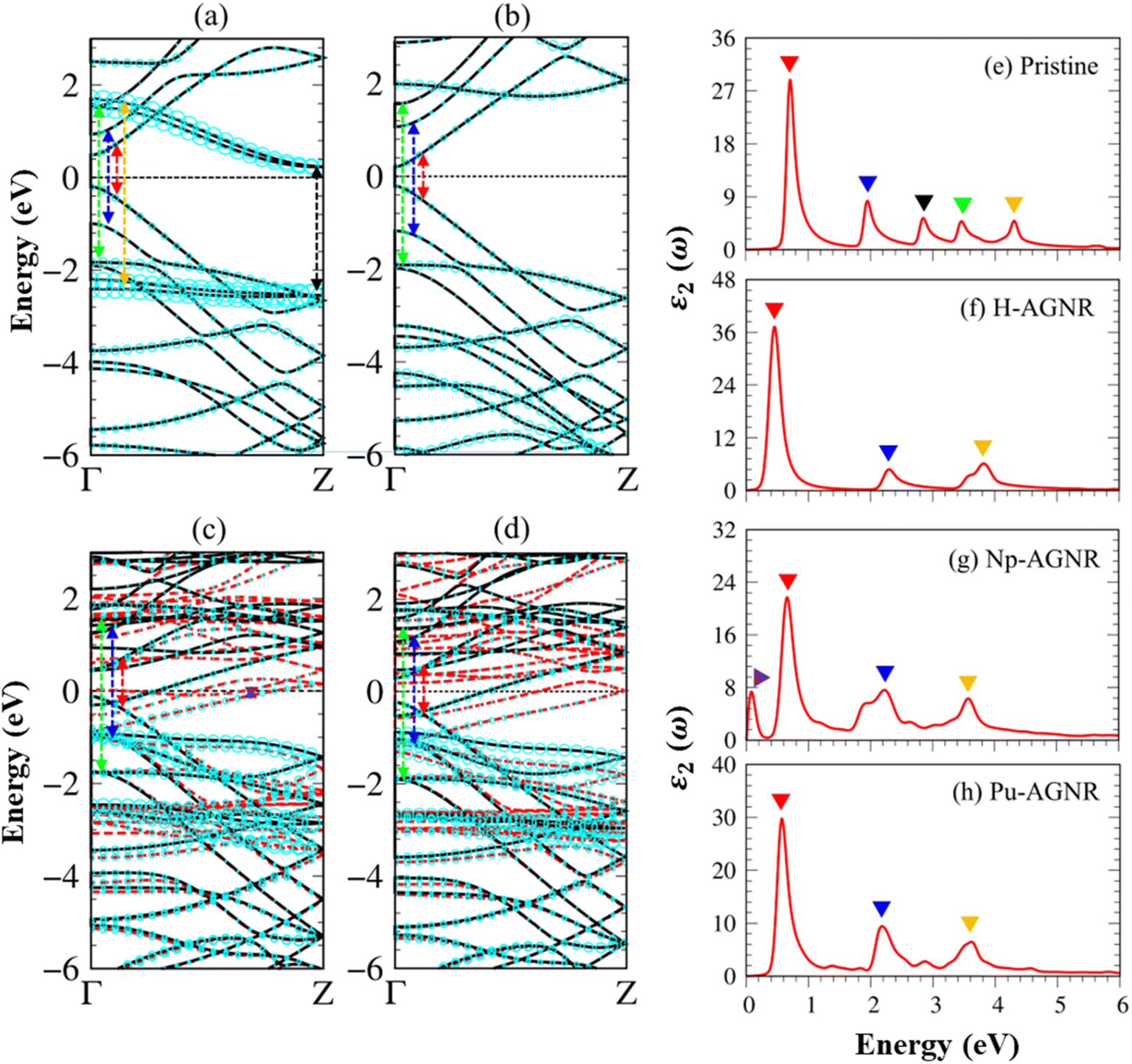 | ||
| Fig. 3 The electronic band structures with carbon-edge-atom-dominance (cyan circles) for (a) pristine AGNRs, (b) H-AGNRs, (c) Np-AGNRs, and (d) Pu-AGNRs. The dashed red and solid black lines correspond to spin-up and spin-down energy bands. The colored arrows represent the vertical optical excitations corresponding to the prominent peaks which show the imaginary part of dielectric functions in the cases: (e) pristine AGNRs, (f) H-AGNRs, (g) Np-AGNRs, and (h) Pu-AGNRs, respectively. | ||
The electronic properties of AGNRs are dramatically altered after hydrogen passivation as shown in Fig. 3b. The edge-atom-created conduction bands and weakly dispersive valence bands vanish for various H-passivated armchair systems, indicating the absence of dangling bonds. These drastic changes in energy bands originate from the strong C–H bonds and the very low bound state energy of H 1s. The co-dominance of C(2s, 2px, 2py) and H 1s orbitals makes important contributions to the valence-occupied states in the range of E < −3.0 eV.
The low-lying band structures, as clearly illustrated in Fig. 3c–d, exhibit dramatic transformations after the edge decorations of the rare-earth metal adatom. There are more 1D energy sub-bands because of the active neptunium/plutonium–carbon orbital hybridizations. Each sub-band is dominated by C or Np/Pu, or co-dominated by (C, Np)/(C, Pu) as will be discussed later in the density of states in Fig. 4a–d. The drastic changes in the band-edge states cover their numbers, energies, critical points, and curvatures. The 1D energy sub-bands also exhibit spin-split behaviors, mainly owing to the 5f orbitals of the rare-earth-metal atoms. Furthermore, the semiconductor–metal transitions come to exist in all rare-earth decoration systems, indicating the generation of metallic bonds. These dominating free carrier densities would induce the observable spin current under a small bias voltage. The 1D rare-earth-metal edge-decorated graphene nanoribbons are expected to create an unusual spintronic.
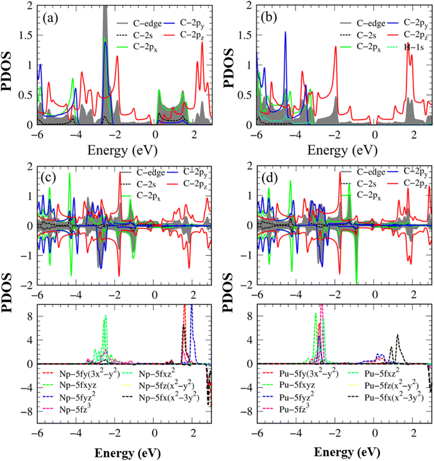 | ||
| Fig. 4 The energy-projected density of states (PDOS) with the atom- & orbital-decomposed spin-split contributions for (a) pristine AGNRs, (b) H-AGNRs, (c) Np-AGNRs, and (d) Pu-AGNRs. | ||
The main features of Van Hove singularities in the density of states39 are easily modulated by the host and guest atoms. In Fig. 4a, the pristine graphene nanoribbon can display a lot of strongly asymmetric peaks across the Fermi level, mainly owing to 1D parabolic energy sub-bands. Any pristine systems have band gaps without free carriers at the Fermi level because of the complicated chemical/physical environments. Most of the π- and σ-electronic Van Hove singularities do not present prominent mergences, indicating perpendicular chemical bonds on a planar honeycomb crystal. The Van Hove singularities of the latter come to exist at the same frequencies, but under different intensities even for px and py orbitals (the destruction of (x, y) plane symmetry). The highest occupied valence states and the lowest unoccupied conduction ones, which account for a band gap, respectively arise from pz and (px, py) orbitals, in which the latter is associated with the carbon edge-atoms. This result differs from those observed in single-layer40 and few-layer graphene systems,41 graphene-like materials16 and δ-IV–VI monolayers,12 where the electronic and hole states arise from pz and pz orbitals, as well as px (py) and py (px) orbitals, respectively.
After being passivated by the hydrogen atoms, the low-lying conduction structures are only dominated by the 2pz orbitals (Fig. 4b); that is, the π bonding determines the low-energy essential properties of the H-passivated armchair graphene nanoribbons. Furthermore, the 1s- and (2s, 2px, 2py)-related asymmetric peaks appear simultaneously, revealing the strong orbital hybridizations among the three orbitals. The behavior reflects the presence of the sp2-s chemical bonding in the C–H bonds.
The number, frequency, and intensity of Van Hove singularities show obvious changes after the Np/Pu edge decorations (Fig. 4c–d), especially for their dominant energy regions −3.50 eV < E < +4.00 eV. As for plutonium (Pu), the significant fourteen-5f orbitals about (5fz3, 5fxz2, 5fyz2, 5fxyz, 5fz(x2 − y2), 5fx(x2 − 3y2), 5fy(3x2 − y2)) reveal comparable contributions; furthermore, there exist important differences between the spin-up and spin-down Van Hove singularities. The spin-split C(2s, 2px, 2py, 2pz) also displays observable differences, in which the C 2pz orbitals create the Fermi-surface band properties. This further illustrates the metallic bonds of C–Pu and Pu–Pu at edge boundaries. From the merged Van Hove singularities, the multi-orbital hybridizations of C–Pu, Pu–Pu and C–C bonds, respectively, exhibit (2s, 2px, 2py, 2pz)–(5fz3, 5fxz2, 5fyz2, 5fxyz, 5fz(x2 − y2), 5fx(x2 – 3y2), 5fy(3x2 − y2)), (5fz3, 5fxz2, 5fyz2, 5fxyz, 5fz(x2 − y2), 5fx(x2 − 3y2), 5fy(3x2 − y2))–(5fz3, 5fxz2, 5fyz2, 5fxyz, 5fz(x2 − 3y2), 5fx(x2 − 3y2), 5fy(3x2 − y2)), and (2s, 2px, 2py)–(2s, 2px, 2py) & (2pz–2pz). Of course, the ferromagnetic spin configurations are driven by the Np/Pu atoms.
In the presence of external electromagnetic field perturbation, electrons within occupied states undergo vertical excitation to unoccupied states. The optical excitation process must adhere to the conservation principles of energy, momentum, and the Pauli exclusion principle.40 The dynamical characteristics of the charge screening could be well defined by the microscopic dimensionless dielectric function ε(ω). According to the Fermi-golden rule, the single-particle excitations are directly related to the imaginary part of dielectric functions:
 | (1) |
Because of the 1D density of states, the optical absorbance spectrum of pristine AGNRs presents at least five square root divergent peaks (Fig. 3e). The optical gap, which is the threshold frequency situated at 0.60 eV, is slightly larger than the indirect band gap. Such rapid oscillation originates from the promotion of C 2pz electrons at the Γ center. The second and the third prominence peaks are correspondingly related to the excitations of C 2pz electrons in the second valence sub-band to the second and the third conduction sub-bands. Very interestingly, the prominent peaks at 3.50 eV and 4.40 eV are due to the dominating orbitals of C(2s, 2px, 2py). Such structures are purely induced by the edge-dangling bond effects. The delicate identifications are achieved from the orbital-decomposed Van Hove singularities; that is, the initial and/or the final states must possess the singular densities of states. It is very important to note that the transitions between the π and σ states are absent even though their joint density of states is significant. This is due to the vanishing of the in-plane matrix element |φxy|pxy|φz|2 in the planar honeycomb lattice.
The optical properties of H-AGNRs (Fig. 3f) are quite different from those of the pristine ones. The optical gap is now located at 0.40 eV and equal to that of the direct electronic band gap. The second and third peaks undergo a blue shift with their transition energy being 2.30 eV and 3.90 eV, respectively. These prominent peaks are all dominated by 2pz → 2pz optical transitions. Interestingly, the fourth and fifth peaks, which are related to the edge dangling bond, have disappeared since their corresponding sub-bands and Van Hove singularities are terminated by the strong C–H covalent bonds.
The optical properties of AGNRs are drastically changed by the Np/Pu edge decorations, e.g., the excitation frequency, intensity, number, and form of prominent absorption peaks. Most effective excitation channels are closely related to the spin-up configurations except for a few ones. Taking Np-AGNRs as an example, the threshold excitation frequency, 0.10 eV, is non-zero even for ferromagnetic metals, mainly owing to the carbon dominance on the spin-up-dependent vertical, as shown in Fig. 3g. This threshold peak in the imaginary part of the dielectric function mainly arises from the initial and final state transition of the C 2px orbitals. The pure π electronic excitations, which possess comparable spin-up and spin-down contributions, come to exist as the second, third, and fourth absorption peaks at 0.62 eV (the red triangle), 2.19 eV (blue triangle), and 3.60 eV (green triangle). The other prominent absorption peaks with very weak intensities belong to the composite Pu-5f orbitals (Fig. 3h). Such phenomena arise from the vanishing of the square of matrix elements under the extreme 5f wave functions. The optical excitation peaks related to carbon edge dangling bonds are dramatically suppressed or reduced due to the rather strong C–Np and C–Pu chemical bonds. The unusual optical excitations induced through the rare-earth decoration achieved in current investigations (Table 2) are rather complicated and may provide useful information for further experiment measurement and real applications, e.g., spintronic techniques.
| System | Peak | Energy (eV) | Orbital hybridizations | Spin polarization |
|---|---|---|---|---|
| Pristine | Red | 0.60 | C(2pz) → C(2pz) | — |
| Blue | 1.90 | C(2pz) → C(2pz) | — | |
| Green | 2.87 | C(2pz) → C(2pz) | — | |
| Cyan | 3.50 | C(2s, 2px, 2py) → C(2s, 2px, 2py) | — | |
| Black | 4.40 | C(2s, 2px, 2py) → C(2s, 2px, 2py) | — | |
| H-AGNRs | Red | 0.40 | C(2pz) → C(2pz) | — |
| Blue | 2.30 | C(2pz) → C(2pz) | — | |
| Cyan | 3.90 | C(2pz) → C(2pz) | — | |
| Np-AGNRs | Yellow | 0.10 | C(2px) → C(2px) | ↑ |
| Red | 0.62 | C(2pz) → C(2pz) | ↑ + ↓ | |
| Blue | 2.19 | C(2pz) → C(2pz) | ↑ + ↓ | |
| Green | 3.60 | C(2pz) → C(2pz) | ↑ + ↓ | |
| Pu-AGNRs | Red | 0.61 | C(2pz) → C(2pz)Pu(5f) → Pu(5f) | ↑ + ↓ |
| ↑ | ||||
| Blue | 2.20 | C(2pz) → C(2pz) | ↑ + ↓ | |
| Green | 3.61 | C(2pz) → C(2pz) | ↑ + ↓ |
4 Conclusions
In conclusion, the geometric, electronic, magnetic, and special spin-dependent optical excitations of pristine AGNRs, H-AGNRs, Np-AGNRs, and Pu-decorated AGNRs were investigated by the first-principles calculations. In particular, the orbital hybridizations between C–C, C–H, C–Np, and C–Pu atoms and the spin interactions are the critical factors affecting the optimized geometric structures, the electronic and magnetic properties, and the optical excitations. The main features cover the planar carbon-honeycomb lattices, the open edge/closed edge of hexagons/pentagons with C–H/C–Np/C–Pu bonds, the dramatic transformations in the spatial charge density distributions under the very strong chemical bonds, the induced magnetic moments due to the contribution of 5f orbitals, the featured band structures with the sensitive atom and spin dominance at distinct energy ranges, the indirect–direct/semiconductor–ferromagnetic-metal transitions and the spin-split configurations after the dangling-bond saturations, and the special optical excitations. The current study is of paramount importance for basic sciences as well as for practical applications, e.g., spintronic techniques.Overall, while rare earth atoms decorated graphene nanoribbons offer exciting opportunities for advanced materials and applications, they also pose challenges related to cost, availability, environmental impact, and complex interactions. However, with further research and innovation, these drawbacks can be addressed, and the strengths of these materials can be harnessed for a wide range of practical applications.
Conflicts of interest
The authors declare no competing interests.Acknowledgements
We extend our heartfelt appreciation to Distinguished Professor Ming-Fa Lin and his laboratory at the Department of Physics, National Cheng Kung University, Tainan City, Taiwan, for their invaluable support and the use of their state-of-the-art facilities and resources, which have greatly enhanced the quality of our current research.References
- A. K. Geim and K. S. Novoselov, “The rise of graphene”, Nat. Mater., 2007, 6(3), 183–191 CrossRef CAS PubMed.
- K. S. Novoselov, A. Mishchenko, A. Carvalho and A. Castro Neto, “2D materials and van der Waals heterostructures”, Science, 2016, 353(6298), aac9439 CrossRef CAS PubMed.
- M. Sprinkle, et al., “First direct observation of a nearly ideal graphene band structure”, Phys. Rev. Lett., 2009, 103(22), 226803 CrossRef CAS PubMed.
- L. Ponomarenko, et al., “Effect of a high-κ environment on charge carrier mobility in graphene”, Phys. Rev. Lett., 2009, 102(20), 206603 CrossRef CAS PubMed.
- A. A. Balandin, et al., “Superior thermal conductivity of single-layer graphene”, Nano Lett., 2008, 8(3), 902–907 CrossRef CAS PubMed.
- F. Scarpa, S. Adhikari and A. S. Phani, “Effective elastic mechanical properties of single layer graphene sheets”, Nanotechnology, 2009, 20(6), 065709 CrossRef CAS PubMed.
- X. Liu, T. H. Metcalf, J. T. Robinson, B. H. Houston and F. Scarpa, “Shear modulus of monolayer graphene prepared by chemical vapor deposition”, Nano Lett., 2012, 12(2), 1013–1017 CrossRef CAS PubMed.
- C. Lee, J. Y. Kim, S. Bae, K. S. Kim, B. H. Hong and E. Choi, “Optical response of large scale single layer graphene”, Appl. Phys. Lett., 2011, 98(7), 071905 CrossRef.
- W.-K. Tse, Z. Qiao, Y. Yao, A. MacDonald and Q. Niu, “Quantum anomalous Hall effect in single-layer and bilayer graphene”, Phys. Rev. B: Condens. Matter Mater. Phys., 2011, 83(15), 155447 CrossRef.
- N. H. Giang, T. T. T. Hanh, N. T. Nga and V. Van Hoang, “Formation of graphene on BN substrate by vapor deposition method and size effects on its structure”, Phys. B, 2018, 534, 26–33 CrossRef.
- T. T. T. Hanh, V. K. Dien, N. T. T. Tran, C.-H. Ho, T. D. H. Nguyen, and M.-F. Lin, Diverse Quasiparticle Properties of Emerging Materials: First-Principles Simulations. CRC Press, 2022 Search PubMed.
- K. Ren, et al., Prediction of 2D IV-VI semiconductors: auxetic materials with direct bandgap and strong optical absorption, Nanoscale, 2022, 14(23), 8463–8473 RSC.
- V. K. Dien, N. Thi Han, W. Bang-Li, K.-I. Lin and M.-F. Lin, “Correlation between orbital hybridizations, phonon spectra, and thermal properties of graphene, germanene, and plumbene”, Phys. Status Solidi RRL, 2023, 17(5), 2200469 CrossRef CAS.
- V. K. Dien, N. T. Han, W. Bang-Li, K. I. Lin and M. F. Lin, “Tuning of the Electronic and Optical Properties of Monolayer GaSe Via Strain”, Adv. Theory Simul., 2023, 6(7), 2200950 CrossRef CAS.
- K. Ren, et al., “Prediction of 2D IV–VI semiconductors: auxetic materials with direct bandgap and strong optical absorption”, Nanoscale, 2022, 14(23), 8463–8473 RSC.
- N. T. Han, V. K. Dien, T.-R. Chang and M.-F. Lin, Optical excitations of graphene-like materials: group III-nitrides, Nanoscale Adv., 2023, 5(18), 5077–5093 RSC.
- N. T. Han, T. Le Manh and V. K. Dien, Direct correlation between electronic and optical properties of the XC monolayers (X= Si, Ge, and Sn) from first-principles calculations, Nanostructures, 2024, 159, 115925 Search PubMed.
- N. T. Han, V. K. Dien, T.-R. Chang and M.-F. Lin, Theoretical investigations of the electronic and optical properties of a GaGeTe monolayer, RSC Adv., 2023, 13(28), 19464–19476 RSC.
- V. K. Dien, P. T. B. Thao, N. T. Han, N. D. Khanh, M.-F. Lin and N. T. Tien, Strain-controlled electronic transport and exciton radiative lifetime in monolayer germanium sulfide, Phys. Rev. B, 2023, 108(20), 205406 CrossRef.
- N. T. Tien, P. T. B. Thao, N. T. Han and V. K. Dien, Symmetry-driven valleytronics in the single-layer tin chalcogenides SnS and SnSe, Phys. Rev. B, 2024, 109(15), 155416 CrossRef.
- N. R. Glavin, et al., “Emerging applications of elemental 2D materials”, Adv. Mater., 2020, 32(7), 1904302 CrossRef CAS PubMed.
- O. Hod, J. E. Peralta and G. E. Scuseria, “Edge effects in finite elongated graphene nanoribbons”, Phys. Rev. B: Condens. Matter Mater. Phys., 2007, 76(23), 233401 CrossRef.
- Q. Chen, L. Ma and J. Wang, “Making graphene nanoribbons: a theoretical exploration”, Wiley Interdiscip. Rev.: Comput. Mol. Sci., 2016, 6(3), 243–254 CAS.
- A. N. Abbas, et al., “Patterning, characterization, and chemical sensing applications of graphene nanoribbon arrays down to 5 nm using helium ion beam lithography”, ACS Nano, 2014, 8(2), 1538–1546 CrossRef CAS PubMed.
- J. Sun, T. Iwasaki, M. Muruganathan and H. Mizuta, “Lateral plasma etching enhanced on/off ratio in graphene nanoribbon field-effect transistor”, Appl. Phys. Lett., 2015, 106(3), 033509 CrossRef.
- Z. Chen, et al., “Synthesis of graphene nanoribbons by ambient-pressure chemical vapor deposition and device integration”, J. Am. Chem. Soc., 2016, 138(47), 15488–15496 CrossRef CAS PubMed.
- Z. Wang, et al., “Tuning the electronic structure of graphene nanoribbons through chemical edge modification: A theoretical study”, Phys. Rev. B: Condens. Matter Mater. Phys., 2007, 75(11), 113406 CrossRef.
- B. Huang, et al., “Adsorption of gas molecules on graphene nanoribbons and its implication for nanoscale molecule sensor”, J. Phys. Chem. C, 2008, 112(35), 13442–13446 CrossRef CAS.
- T. Martins, R. H. Miwa, A. J. Da Silva and A. Fazzio, “Electronic and transport properties of boron-doped graphene nanoribbons”, Phys. Rev. Lett., 2007, 98(19), 196803 CrossRef CAS PubMed.
- Q. Dai, Y. Zhu and Q. Jiang, “Electronic and magnetic engineering in zigzag graphene nanoribbons having a topological line defect at different positions with or without strain”, J. Phys. Chem. C, 2013, 117(9), 4791–4799 CrossRef CAS.
- Y.-T. Lin, H.-C. Chung, P.-H. Yang, S.-Y. Lin and M.-F. Lin, “Adatom bond-induced geometric and electronic properties of passivated armchair graphene nanoribbons”, Phys. Chem. Chem. Phys., 2015, 17(25), 16545–16552 RSC.
- V. K. Nishad, A. K. Nishad, B. K. Kaushik and R. Sharma, “First-principle analysis of transition metal edge-passivated armchair graphene nanoribbons for nanoscale interconnects”, IEEE Trans. Nanotechnol., 2021, 20, 92–98 CAS.
- P. Narin, J. A. Abbas, G. Atmaca, E. Kutlu, S. Lisesivdin and E. Ozbay, “Ab initio study of electronic properties of armchair graphene nanoribbons passivated with heavy metal elements”, Solid State Commun., 2019, 296, 8–11 CrossRef CAS.
- J. Hafner, “Ab-initio simulations of materials using VASP: Density-functional theory and beyond”, J. Comput. Chem., 2008, 29(13), 2044–2078 CrossRef CAS PubMed.
- L. S. Pedroza, A. J. da Silva and K. Capelle, “Gradient-dependent density functionals of the Perdew-Burke-Ernzerhof type for atoms, molecules, and solids”, Phys. Rev. B: Condens. Matter Mater. Phys., 2009, 79(20), 201106 CrossRef.
- P. E. Blöchl, “Projector augmented-wave method”, Phys. Rev. B: Condens. Matter Mater. Phys., 1994, 50(24), 17953 CrossRef PubMed.
- Y.-X. Yu, “Effect of defects and solvents on silicene cathode of nonaqueous lithium–oxygen batteries: a theoretical investigation”, J. Phys. Chem. C, 2018, 123(1), 205–213 CrossRef.
- F. Aryasetiawan, K. Karlsson, O. Jepsen and U. Schönberger, “Calculations of Hubbard U from first-principles”, Phys. Rev. B: Condens. Matter Mater. Phys., 2006, 74(12), 125106 CrossRef.
- P. Kim, T. W. Odom, J.-L. Huang and C. M. Lieber, “Electronic density of states of atomically resolved single-walled carbon nanotubes: Van Hove singularities and end states”, Phys. Rev. Lett., 1999, 82(6), 1225 CrossRef CAS.
- V. K. Dien, W.-B. Li, K.-I. Lin, N. T. Han and M.-F. Lin, “Electronic and optical properties of graphene, silicene, germanene, and their semi-hydrogenated systems”, RSC Adv., 2022, 12(54), 34851–34865 RSC.
- P. Rosenzweig, H. Karakachian, D. Marchenko, K. Küster and U. Starke, “Overdoping Graphene beyond the van Hove Singularity”, Phys. Rev. Lett., 2020, 125(17), 176403 CrossRef CAS PubMed.
- V. K. Dien, N. T. Han, W.-P. Su and M.-F. Lin, “Spin-dependent optical excitations in LiFeO2”, ACS Omega, 2021, 6(39), 25664–25671 CrossRef CAS PubMed.
| This journal is © The Royal Society of Chemistry 2024 |