
 Open Access Article
 This Open Access Article is licensed under a Creative Commons Attribution-Non Commercial 3.0 Unported Licence
Strain engineering of the mechanical properties of two-dimensional WS2†
Yarden Mazal
Jahn
a,
Guy
Alboteanu
 a,
Dan
Mordehai
b and
Assaf
Ya'akobovitz
*a
a,
Dan
Mordehai
b and
Assaf
Ya'akobovitz
*a
aDepartment of Mechanical Engineering, Faculty of Engineering Sciences, Ben-Gurion University of the Negev, Israel. E-mail: assafyaa@bgu.ac.il
bFaculty of Mechanical Engineering, Technion Israel Institute of Technology, Haifa, Israel
First published on 1st July 2024
Abstract
Tuning the physical properties of two-dimensional (2D) materials is crucial for their successful integration into advanced applications. While strain engineering demonstrated an efficient means to modulate the electrical and optical properties of 2D materials, tuning their mechanical properties has not been carried out. Here we applied compressive strain through the buckling metrology to 2D tungsten disulfide (WS2), which demonstrated mechanical softening manifested by the reduction of its effective Young's modulus. Raman modes analysis of the strained WS2 also showed strain-dependent vibrational modes softening and revealed its Grüneisen parameter (γE2g = 0.29) and its shear deformation potential (βE2g = 0.56) – both are similar to the values of other 2D materials. In parallel, we conducted a molecular dynamic simulation that confirmed the validity of continuum mechanics modeling in the nanoscale and revealed that due to sequential atomic-scale buckling events in compressed WS2, it shows a mechanical softening. Therefore, by tuning the mechanical properties of WS2 we shed light on its fundamental physics, thus making it an attractive candidate material for high-end applications, such as tunable sensors and flexible optoelectronic devices.
Introduction
Two-dimensional (2D) tungsten disulfide (WS2), a layered material that comprises tungsten atoms sandwiched between two layers of sulfide atoms, is a member of transition metal dichalcogenides (TMDs) 2D materials and has attracted immense scientific attention due to its extraordinary physical properties. WS2 is among the strongest members in the TMDs family with Young's modulus exceeding 300 GPa for a single-layer,1 it has high electrical conductivity and high excitation band energy.2 These properties made WS2 attractive for a wide range of applications, such as flexible photodetectors,3 field effect transistors (FET),4 resonators,5 and a variety of sensors.6,7The mechanical properties of TMDs have been under intense focus as they have a crucial influence on the operation of functional devices. While the indentation method was widely used to investigate the mechanical properties of suspended TMDs,8–12 other methods were suggested as well, including resonance characterization,13,14 bulge test (pressurized cavity test),15 and the micro-Brillouin light scattering method.16 The buckling method, which we use in the current study, was recently employed on 2D materials and allowed the mechanical analysis of thin layers (e.g., both TMDs17 and other 2D materials18). In this method, a controlled uniaxial strain is transferred from a compliant substrate to a thin film, and the deformed (wrinkled) shape of the latter is used to extract its elastic properties.
The studies carried out so far demonstrated the resilience and high stretchability of WS2 and other TMDs,19 that makes them suitable materials for strain engineering analyses. In strain engineering experiments the atomic structure of the investigated material is modified by means of controlled application of mechanical deformation, which allows the tuning of their properties. Specifically, since energy states are tightly bound in TMDs, they show strong coupling between the applied strain and their energy structure. As a result, many studies used strain engineering for bandgap modulation. For example, WSe2 demonstrated optical band-gap reduction under uniaxial strain,20 while bandgap tuning of WS2 was demonstrated through local buckling deformation.21 An enhanced photoluminescence signal of WS2 was observed under tensile strain due to direct excitonic recombination.22 Furthermore, the bandgap modulation of MoS2 was reported under bi-axial compression and tension,23 uniaxial tension,24 and pure shear.25 Other works demonstrated the use of strain engineering to enhance the piezoelectric properties of TMDs,26 their magnetic properties,27 and phonon vibration.28 First principle calculations often accompanied the experimental studies and theoretically confirmed the impact of strain engineering on the band structure of TMDs.24 Despite the intense research on strain engineering of TMDs, its impact on their mechanical behavior is yet to be understood.
In this study, we bridge this knowledge gap. We first applied compression to thin layered WS2. Prior to investigating it using a continuum mechanics model, we verified its validity by comparing it to an atomistic MD model. Then we extract the effective Young's modulus using Bernoulli–Euler continuum mechanics model and use a modified molecular dynamics (MD) simulation to further clarify our results. We also conducted a Raman analysis of compressed WS2 to improve our understanding and validate our results. We showed that compressed WS2 demonstrates mechanical softening, manifested by reduction of its effective Young's modulus and redshift of its Raman vibrational modes, due to atomic-scale buckling events.
Methods
The buckling metrology
We studied the behavior of few-layered WS2 flakes under compressive strains ranging between 0.3% and 4%. We clamped polydimethylsiloxane (PDMS) substrate to movable stages (Fig. 1a(I)) and stretched the PDMS by bringing the stages apart (Fig. 1a(II)). Then, we mechanically transferred a thin WS2 flake via scotch tape exfoliation from a solid crystal to the substrate of the stretched PDMS (Fig. 1a(III)). Next, by bringing the stages closer we transferred the strain from the PDMS to the WS2, thus compressing it and creating wrinkles due to buckling (Fig. 1a(IV)). A high-resolution digital optical microscope (Keyence VHX-5000, magnification ×2000) was used to capture the wrinkles obtained under different strains, Fig. 1b. A scanning electron microscope (SEM) image of a compressed flake is shown in Fig. 1c. Optical images of the wrinkled WS2 were post-processed using a fast Fourier transform (FFT) analysis implemented on MATLAB software that revealed the spatial frequency of the wrinkles (inset of Fig. 1b).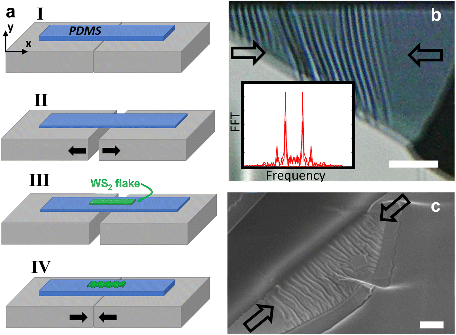 | ||
| Fig. 1 (a) Illustration of the buckling metrology. PDMS is shown as the blue layer while the WS2 flake is represented as the green layer. (b) Optical image of strained WS2. Scale bar: 5 μm. Inset: FFT of the image. (c) SEM image of strained WS2. Scale bar: 1 μm. The arrows denote the direction of the applied strain. | ||
Knowing the thickness of the WS2 flakes is essential for their analysis (see details below). However, since measuring the flakes thicknesses on the relatively soft PDMS substrate is challenging, after completing the buckling experiments we transferred the flakes to Si/SiO2 wafer and measured their thicknesses using an atomic force microscope (AFM).
Molecular dynamics simulations
We performed molecular dynamics (MD) simulations to improve our understanding of the behavior of the WS2. We employed the open-source code LAMMPS29 for the MD simulation. We adopted a modified version of the Stillinger–Weber (SW) potential for TMDs, as was done in similar studies.30 This interatomic potential was found to properly describe the interlayer interaction between W and S atoms. We initiated our theoretical analysis with an MD simulation of a monolayer WS2 and then performed an analysis of a few layered WS2 structure.In the monolayer MD simulation, a rectangular computational cell was constructed with a unit cell composed of six atoms (two W atoms and four S atoms, Fig. 2a). We considered periodic boundary conditions along the sheet axes in the x- and y-directions. An example of a sheet with five unit cells in each direction is shown in Fig. 2b. First, the atom positions were relaxed, in combination with the relaxation of the unit cell size in the x- and y-directions to nullify the internal stresses, using the conjugate gradient algorithm. Then, initial velocities are assigned to the atoms that correspond to a velocity of 300 K, followed by MD timesteps using the microcanonical ensemble. During the MD simulations, a constant strain rate of 107 s−1 is applied along the x-direction.
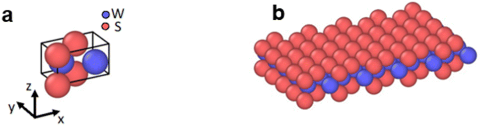 | ||
| Fig. 2 MD simulation. W and S atoms are denoted as purple and red colored spheres. (a) MD unit cell. (b) MD sheet. | ||
Experimental results and discussion
Buckling experiment
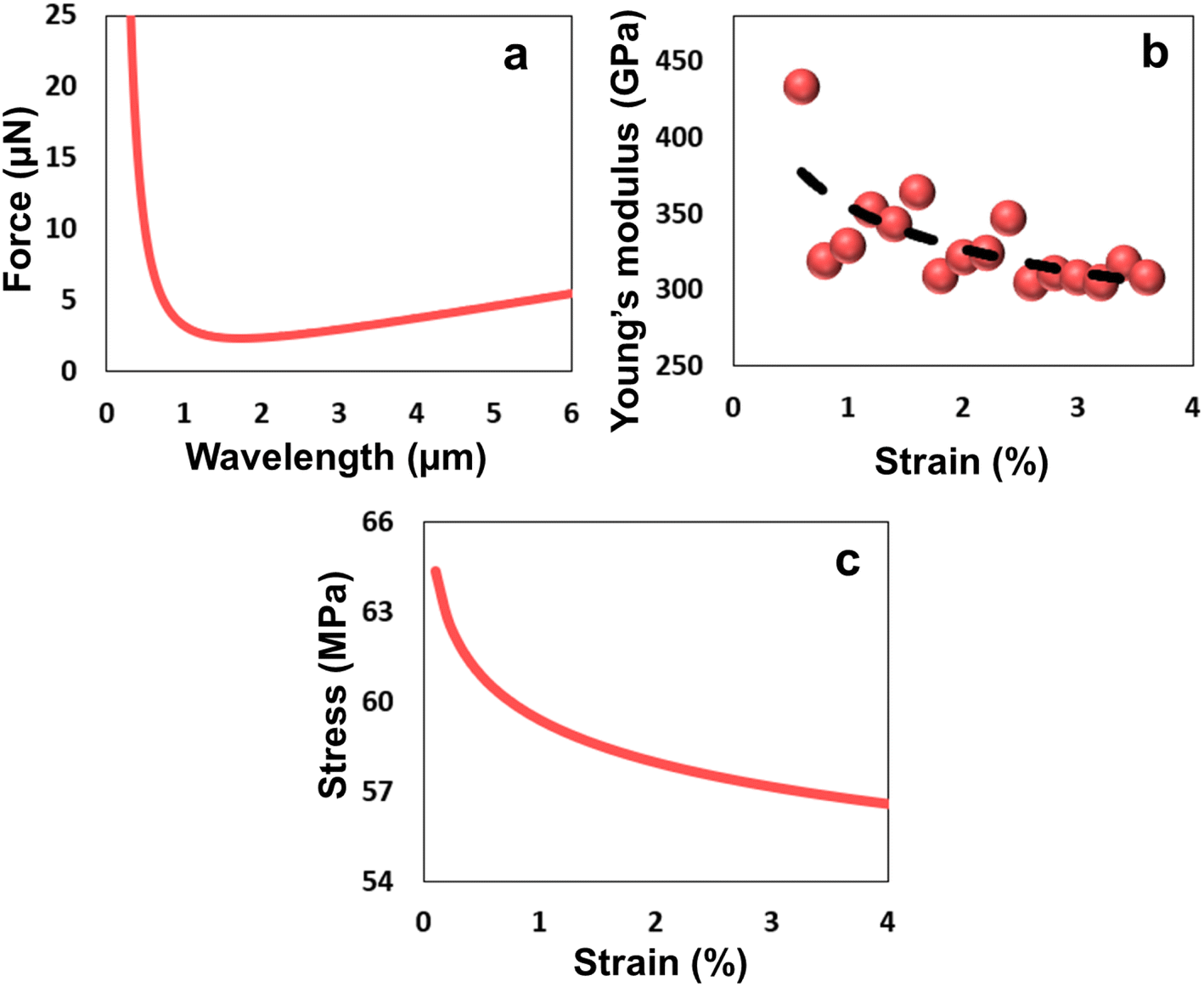
We initiated our experiments by applying 4% strain to the PDMS, transferring the WS2 flake, and gradually releasing the stretch of the PDMS, thereby compressing the flake. Importantly, prior to the application of the buckling, we did not observe wrinkles in the WS2. During the transfer of the strain to the WS2 we captured optical images of the wrinkles (e.g., Fig. 1b), from which we extracted their wavelength, λ, that is inversely proportional to the spatial frequency. The thickness was obtained after the buckling experiment, as we transferred the WS2 flakes to a Si/SiO2 wafer and measured their thickness using AFM (Cypher-ES, Oxford Instruments), Fig. 3a. The relationship between the wavelength and the compressive strain demonstrated a reduction of the wavelength as we increased the strain, see Fig. 3b obtained for a flake subjected to compressive strain.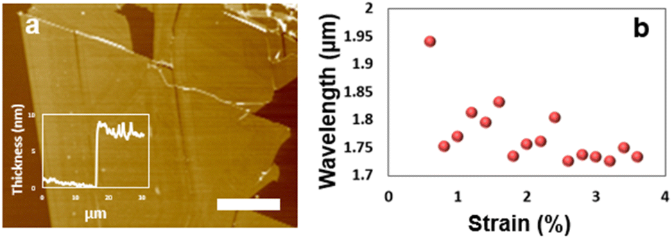 | ||
| Fig. 3 (a) Thickness measurement of the WS2 flake using AFM after transfer to Si/SiO2 wafer. Scale bar: 10 μm. (b) The relationship between the wavelength and the compressive strain. | ||
Validation of continuum model
Several studies analyzed the results obtained from buckling metrology through continuum models. Contrary to first principal calculations, such continuum models are beneficial since they are computationally cheap and they take into account large-scale phenomena, such as the micron-scale wrinkles we observed in our experiments. In addition, previous studies showed that continuum mechanics models reliably describe mechanical behavior at the nanoscale. For example, continuum model previously described the buckling of carbon nanotubes,31 while the Bernoulli–Euler beam theory was employed to describe the vibrations of a nano foam.32We checked the validity of the continuum model through a comparison of its results to those obtained from the MD atomistic model. We examined a WS2 free-standing monolayer under compression. When the WS2 monolayer is subjected to compression in the MD simulation, it first linearly and uniaxially compresses, followed by its buckling, insets of Fig. 4a. An example of the stress–strain curve and the buckled shape is shown in Fig. 4a. We extracted pre-buckled Young's modulus of WS2 monolayer from the slope of the linear part of the stress–strain curve, such that Emonolayer = 404 ± 17 GPa. This value is in reasonable agreement with theoretical estimations reported elsewhere.1 Importantly, since we do not control the crystal orientation in the experiments, a similar analysis was conducted by applying the strain in a perpendicular direction to the one shown in Fig. 4a. For brevity, we do not show the stress–strain response in this direction, since a similar behavior was obtained, with Young's moduli in the range 418 ± 6 GPa. In addition, we found that the physical size of the MD model (i.e., the number of atoms per unit cells included in the model) weakly influenced the calculated Young's modulus.
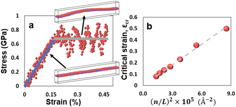 | ||
| Fig. 4 MD analysis results of WS2 monolayer. (a) Stress–strain response. The solid lines are the averaged linear elastic curve (blue line) and the buckled curve (gray line). Insets: the pre-buckled (lower inset) and buckled (upper inset) shapes. (b) The critical buckling strain as a function of (n/L)2. A linear fit is drawn as a dashed line. | ||
The linear pre-buckling deformation is terminated by the buckling of the film, accompanied by stress fluctuations. At this stage, we limit ourselves to a small strain range after buckling, and we consider the average post-buckling stress to be constant at this strain range (gray line in Fig. 4a). This average stress represents the bending rigidity of the buckled monolayer. The fluctuations are a result of the high-frequency waves generated after buckling. Since we are employing periodic boundary conditions, the length of the box affects the buckling strain. To examine this dependency, we compare the MD simulation results to those obtained from a continuum model. We model the WS2 monolayer as a sheet having bending rigidity and subjected to an axial force, such that it obeys the following governing equation
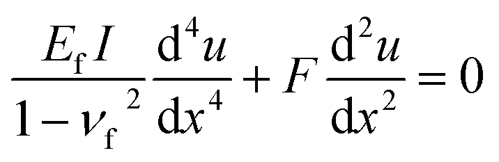 | (1) |
 | (2) |
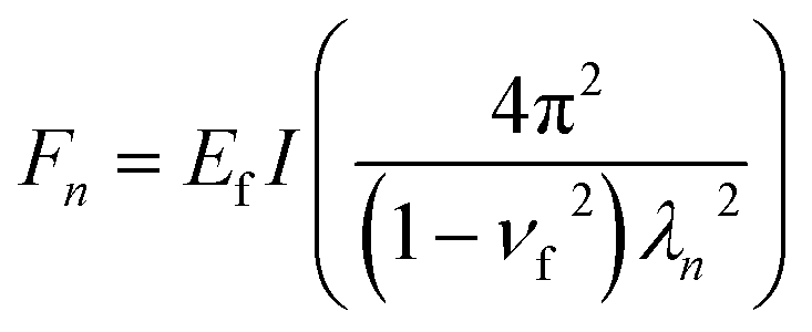
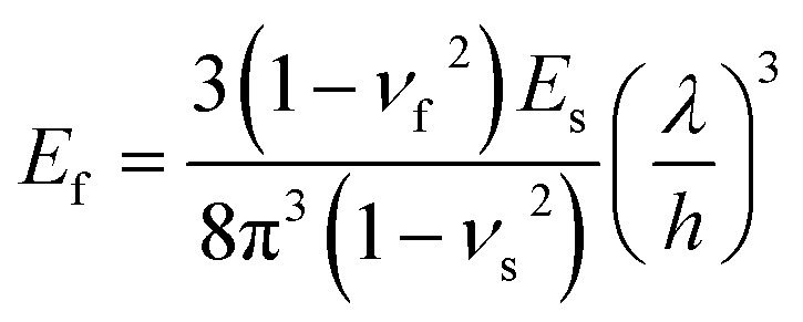
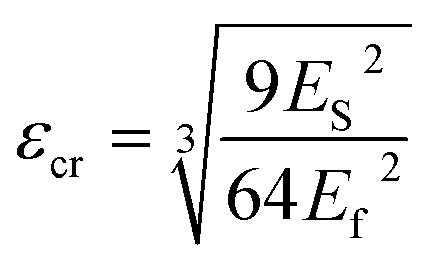
We assume that the atomic sheet behaves like a continuum sheet of width h and νf = 0, such that the corresponding buckling strain is
 | (3) |
We plot in Fig. 4b the buckling strains extracted from the MD simulations (red markers), which correspond to the first buckling mode, and the continuum model prediction obtained from eqn (3) (dashed line) as a function of (n/L)2. Fitting the continuum model to the MD results yields the effective thickness of h = 4.3 Å. When applying the load in the perpendicular direction, a similar relation between the critical buckling strain and the cell size was found, with an effective thickness of h = 4.2 Å. The similar values in both directions, in addition to the outcome of eqn (3) which is indifferent to the compression direction, demonstrate the accuracy of treating this atomically-thin system on the continuum level, regardless of the compression direction. Additionally, this effective thickness is comparable to the reported distance between the atoms along the thickness of the layer film (about 3.1 Å). Therefore, we conclude that although some reasonable quantitative difference arises from the continuum model, this model gives a good description of the mechanical behavior and a rough quantitative estimation of the buckling stress and strain.
Buckling experiment analysis
We modify our continuum model to include the unit force applied by the elastic substrate (the PDMS), such that the WS2 monolayer obeys the following governing equation33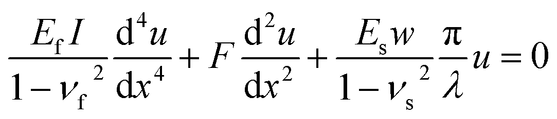 | (4) |
Eqn (4) describes the behavior of a slender mechanical element with bending rigidity and constrained to an elastic support. Our observations indicate that due to the micron-scale deflection of the buckled WS2 compared to the millimeter-scale thickness of the PDMS, both materials maintained contact after buckling took place. Importantly, we excluded from our analysis experiments, in which the WS2 detached from the PDMS and slipped. A solution of eqn (4) is a sinusoidal deflection of the flake, namely
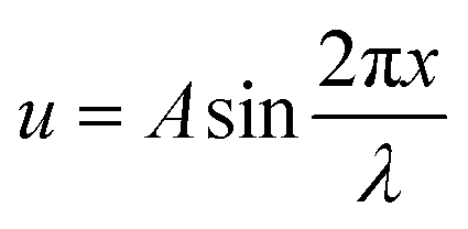 | (5) |
 | (6) |
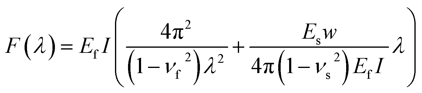
The axial force has a minimum at a certain wavelength, λ (Fig. 5a). If the load is lower than that minimum, the flake is stable (i.e., it does not wrinkle/buckle). On the other hand, if the load is higher than the minimum value, the flake is unstable and wrinkles according to eqn (5). Thus, the minimum force value, obtained at dF/dλ = 0, represents the force at which buckling occurs, which yields the following term
 | (7) |
 | ||
| Fig. 5 (a) Axial force versus wavelength derived from eqn (6). (b) Experimental effective Young's modulus of WS2 as the function of the applied strain. (c) Post-buckling stress–strain curve extracted from the experiment. | ||
The critical buckling strain, namely the strain at which wrinkles first appear, is evaluated as follows
 | (8) |
Eqn (8) implies that when Young's modulus of the thin flake is significantly higher than that of the substrate, as occurs in our case, the buckling appears under small compressive strain.
Eqn (7) gives the relationship between the Young's modulus and the measured wavelength, thus we use it to extract the effective Young's modulus of the wrinkled WS2. The measured effective Young's modulus is shown in Fig. 5b for a representative compressed flake, and demonstrates a decrease in its value when increasing the compressive strain, namely softening behavior. Notably, previously reported density functional theory (DFT) analysis predicted the opposite trend, namely stiffening under compression (we clarify this discrepancy in the discussion below).36
We substitute the extracted Young's modulus, the wavelength, and material constants into the force term written in eqn (6), and we calculated the stress (σ = F/Â, where  is the cross-section area) to get an experimental evaluation of the stress–strain curve of the WS2, see Fig. 5c (the flake dimensions were estimated as w = 10 μm and h = 6 nm). This curve demonstrates a decrease in the stress when increasing the compressive strain. This behavior also describes softening, as it reflects lower elastic resistance of the flake.
Raman analysis under compression
We performed in situ Raman spectra experiments, in which we acquired the Raman spectra of strained WS2 samples (compressive strain ranged from 0% to 2%). We used a LabRam HR Evolution Horiba Raman system with a 532 nm laser, ×100 objective, and an intensity of 0.6 mW to avoid damage to the samples. The Raman spectra of WS2 (ref. 37 and 38) and other strain-engineered TMDs were thoroughly investigated in the literature.39–41 TMDs presented Raman vibrational modes that are highly sensitive to the applied strain due to phonon coupling to the strain. We show the Raman spectra of a representative strained WS2 in Fig. 6a. Unstrained WS2 usually shows the doubly degenerated in-plane vibrational mode that appears at 350 cm−1 and the out-of-plane vibrational mode
  at 410 cm−1. Previous studies showed that when increasing the strain, the degenerated
  peak splits into two subpeaks,
  and
and  due to the symmetry breaking of the WS2 crystal.42 In some of our samples we observed the splitting of the in-plane vibrational mode peak already in the unstrained spectra, which we attribute to some preliminary stresses that exist due to the exfoliation process (an example for a sample with no initial splitting is shown in the ESI†). When we applied compressive strain all peak positions (
 and
and  modes) redshifted with the increasing strain (Fig. 6b–d), indicating vibrational modes softening in the WS2. Importantly, this observation agrees with the mechanical softening observed in our buckling experiment. Also, similar Raman mode softening observed in other strained TMDs was reported in the literature.10,39,42,43
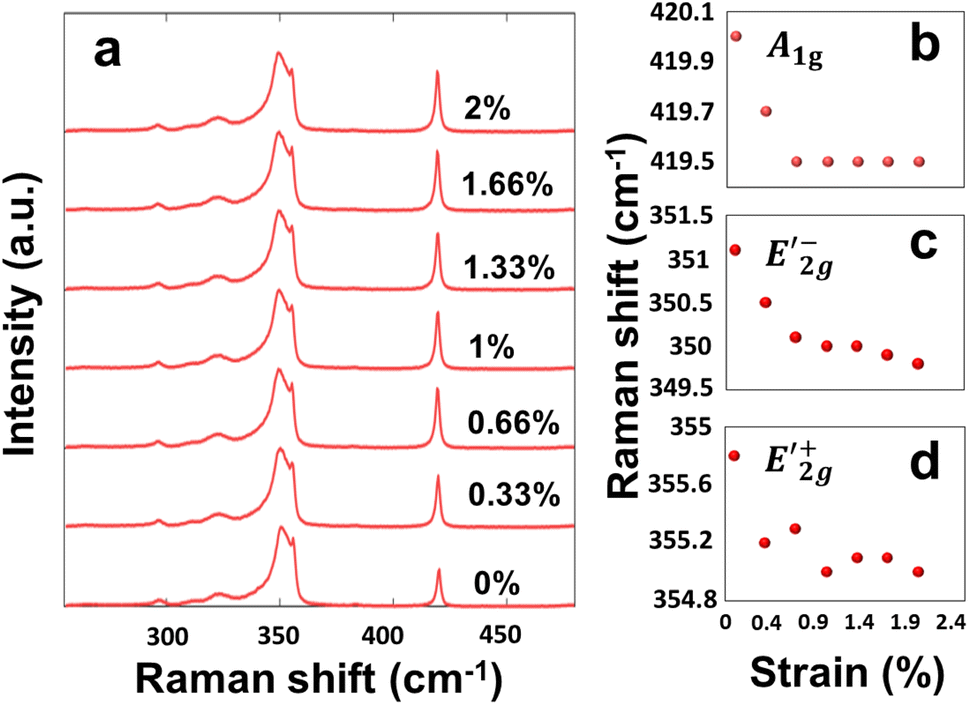 | ||
Fig. 6 (a) Raman spectra of strained WS2. (b–d) Raman peak's location shifts for A1g,  and and  | ||
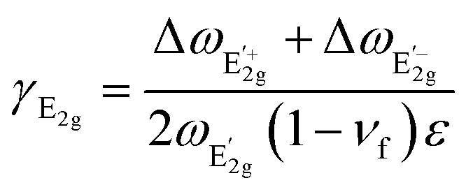
The strain-dependent  Raman peaks allow us to calculate the Grüneisen parameter, γE2g, which is proportional to the shift rate of phonons and determines the thermodynamic properties of the crystal. In addition, the symmetry breaking of the lattice allows us to estimate the shear deformation potential, βE2g, which represents the required energy to induce shear deformation, such that44
 | (9) |
 | (10) |
 is the frequency of the
  modes,
  and
and  are the frequency shifts of the
  and
and 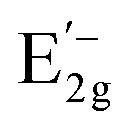 peaks, respectively. In addition, νf is the Poisson's ratio of the WS2 flake and ε is the applied compressive strain. We obtained that the Grüneisen parameter is γE2g = 0.29, which is similar to the values obtained for other TMDs (e.g., 1.1 for MoS2 and 0.38 for WSe2) and to the value reported for WS2 (0.5),45 and smaller than Grüneisen parameter values obtained for graphene (1.99)46 and hexagonal boron-nitride (hBN, 1.88).45 We calculated the shear deformation potential of βE2g = 0.56, which is again similar to other TMDs (e.g., 0.78 for MoS2 and 0.10 for WSe2) and to the values reported for WS2 (0.14), while graphene (0.99) and hBN (0.91) showed larger values.
Bilayer MD simulation
We modified our MD model to gain more insights regarding the softening observed in our experiments. We assumed a bilayer WS2 and employed a Lennard-Jones (LJ) potential as a simple model for the adhesion between the layers. The LJ potential is defined between the S atoms, with a LJ distance of 5.8 Å. Different LJ energies were examined to represent different interlayer adhesions. In Fig. S1 in the ESI,† we show the buckling strain when considering two layers for different LJ energies. The main difference was found to be in short periodicity, where interlayer shear stress is more influential, and thus, the approximation of the Kirchhoff–Love plate theory is not valid. However, for long films, as taken in our simulations, the effect of the adhesion between the layers on the buckling strain is smaller and can be included in the value of the effective thickness, h. When considering the LJ energy of 0.1, 0.2, and 0.5 eV, the effective widths were found to be 13.6 Å, 14.9 Å, and 15.1 Å, respectively. These values are comparable to the reported distance between the atoms in the bilayer film (about 12.1 Å).To date, we are not familiar with a proper interatomic potential for the interlayer interaction, however, we do not aim in this work to make a quantitative comparison with the experimental results. Nonetheless, the simulations above demonstrate the validity of the continuum analysis for these thin 2D structures, which ratifies the use done in the analysis of the experimental study, and we employ the atomistic model to qualitatively explain the strain-dependent Young's modulus in the experiments. Thus, in the following, we consider a bilayer WS2 with LJ interlayer energy of 0.1 eV to extract insights regarding the post-buckling behavior.
Similar to the case of monolayer simulation, the MD simulation of the WS2 bilayer shows that first, the WS2 demonstrates a linear pre-buckling relationship between the stress and strain. Again, since the buckling is abrupt, stress waves are generated and to follow the overall stress response, we reduced the simulated post-buckling strain rate by an order of magnitude to capture these waves. Additionally, the stress response is averaged over a strain range of 0.035% to clarify the mechanical response of the WS2 to compression.
In Fig. 7 we plot the normalized stress (the stress divided by the buckling stress)–strain curve of a 540 Å long film with periodic boundary conditions. The film first deforms elastically up to a buckling stress, σcr, after which it buckles into the first mode (Fig. 7b). As explained, after buckling the stress of the WS2 largely fluctuates, but on average the buckled film still resists compression. Right after buckling, the average compressive stress reduces by ∼25%. During compression, the thin film retains its buckling mode shape up to about a certain strain (1.5% in the chosen example). Beyond this value, we observed an additional stress drop which corresponds to a shape change, in which the buckled shape developed straight segments connected with rounded parts with a small radius of curvature (we further demonstrate this buckled shape in ESI†). This shape change, which is beyond the scope of the present study, can be related to faceting that was found to be related to the interatomic interaction between layers in 2D materials.47
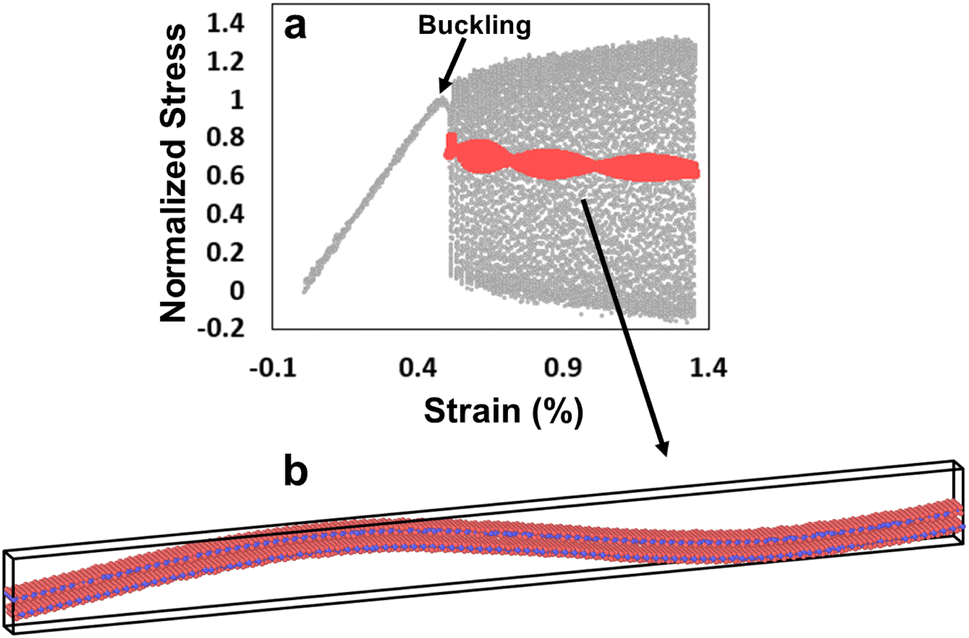 | ||
| Fig. 7 (a) MD simulation for the normalized stress–strain response of a bilayer WS2 including the post-buckling response. To reduce the effect of the fluctuations, a moving average is applied to the post-buckling response (red dots). (b) The buckled shape. | ||
Discussion
Previous theoretical studies showed that the interatomic distance decreases under compression, which results in the dominance of repelling forces in the interatomic interactions.36 As a result, the WS2 is more resistant to an external load, namely, it shows stiffening. However, our buckling experiments demonstrated different behavior, as we observed a decrease in the stress under compression, which indicates a softening of the WS2. Our MD simulations show that atomic scale buckling events occur under compressive strain, which results in a significant shape change of the WS2 to the buckled shape, and thus, also a reduction of its capability to resist external loads. Consequently, we witnessed a mechanical softening. This was further backed by Raman measurements that demonstrated the softening of vibrational modes.Some differences exist between the MD simulations and the experiments. For example, due to limited computation power, only a few layers and a small number of atoms can be included in our simulations. In addition, the nature of the interlayer interaction still requires further study to fully understand its behavior. Nevertheless, and although we did not aim to make a quantitative comparison with the experiments, the MD analysis provided important qualitative insights that clarify our experiments and revealed the reason for the observed softening behavior.
Previous studies demonstrated the ability of various strain engineering methods to modulate the energy structure of the investigated materials, and therefore, tune their Raman spectra and photoluminescence emission. However, the ability to tune the mechanical properties has not been reported. Therefore, we shed light on the fundamental coupling between the atomic structure of WS2 and its mechanical behavior. This understanding will impact the operation of WS2 in applicative systems where they are subjected to mechanical strain, such as flexible electronics and reinforcement of composite materials. This, in turn, will also open the path for new applications that will benefit from the tunability of the mechanical properties of 2D materials, such as smart sensors and adjustable materials.
Summary
We investigated how strain engineering of thin-layered WS2 influences its mechanical behavior. We experimentally applied buckling load to thin layered WS2 and witnessed the softening of its effective Young's modulus. Raman analysis of compressed WS2 backed this behavior as we observed redshift and softening of its vibrational modes. In parallel, we applied MD simulations that confirmed the validity of continuum mechanics models and revealed that under compressive load the thin layer presented atomic-scale buckling events. As a result, the WS2 is subjected to a significant shape change that alters its ability to resist external load and is manifested by mechanical softening. Therefore, we uncover the mechanics underlying strained WS2 and demonstrate the ability to tune its mechanical properties. This ability will be useful for future smart applications.Data availability
The data supporting the article “Strain Engineering of the Mechanical Properties of Two-Dimensional WS2” by Y. M. Jahn, G. Alboteanu, D. Mordehai, and A. Ya'akobovitz are included within the figures in the article and its ESI† files.Conflicts of interest
There are no conflicts to declare.Acknowledgements
We would like to thank Juergen Jopp for his assistant and devotion regarding the AFM measurements. We also want to thank Roxana Golan for her assistance with the SEM measurements.References
- A. Falin, M. Holwill, H. Lv, W. Gan, J. Cheng, R. Zhang, D. Qian, M. R. Barnett, E. J. G. Santos, K. S. Novoselov, T. Tao, X. Wu, L. H. Li and T. D. Ws, Mechanical Properties of Atomically Thin Tungsten Dichalcogenides: WS2, WSe2, and WTe2, ACS Nano, 2021, 15, 2600–2610, DOI:10.1021/acsnano.0c07430.
- H. Kim, H. Kim, J. Lee, H. Lee, D. Choi, J. Lee, W. H. Lee, S. H. Jhang, B. H. Park, H. Cheong, S. Lee and H.-J. Chung, Engineering Optical and Electronic Properties of WS2 by Varying the Number of Layers, ACS Nano, 2015, 7, 6854–6860, DOI:10.1021/acsnano.5b01727.
- A. S. Aji, P. Solís-fernández, H. Goo Ji, K. Fukuda and H. Ago, High Mobility WS2 Transistors Realized by Multilayer Graphene Electrodes and Application to High Responsivity Flexible Photodetectors, Adv. Funct. Mater., 2017, 17, 1703448, DOI:10.1002/adfm.201703448.
- O. A. Abbas, I. Zeimpekis, H. Wang, A. H. Lewis, N. P. Sessions, M. Ebert, N. Aspiotis, C.-C. Huang, D. Hewak, S. Mailis and P. Sazio, Solution-Based Synthesis of Few-Layer WS2 Large Area Continuous Films for Electronic Applications, Sci. Rep., 2020, 10, 1696, DOI:10.1038/s41598-020-58694-0.
- Y. Ben-Shimon, V. Bhingardive, E. Joselevich and A. Ya’Akobovitz, Self-Sensing WS2 Nanotube Torsional Resonators, Nano Lett., 2022, 19, 8025–8031, DOI:10.1021/acs.nanolett.2c01422.
- T. Järvinen, G. S. Lorite, J. Peräntie, G. Toth, S. Saarakkala, V. K. Virtanen and K. Kordas, WS2 and MoS2 thin film gas sensors with high response to NH3 in air at low temperature, Nanotechnology, 2019, 30, 405501 CrossRef PubMed.
- A. S. Pawbake, R. G. Waykar, D. J. Late and S. R. Jadkar, Highly Transparent Wafer-Scale Synthesis of Crystalline WS2 Nanoparticle Thin Film for Photodetector and Humidity-Sensing Applications, ACS Appl. Mater. Interfaces, 2016, 8, 3359–3365, DOI:10.1021/acsami.5b11325.
- D. Y. Khang, J. A. Rogers and H. H. Lee, Mechanical Buckling: Mechanics, Metrology, and Stretchable Electronics, Adv. Funct. Mater., 2009, 19(10), 1526–1536, DOI:10.1002/adfm.200801065.
- A. Falin, Q. Cai, E. J. G. Santos, D. Scullion, D. Qian, R. Zhang, Z. Yang, S. Huang, K. Watanabe, T. Taniguchi, M. R. Barnett, Y. Chen, R. S. Ruoff and L. H. Li, Mechanical Properties of Atomically Thin Boron Nitride and the Role of Interlayer Interactions, Nat. Commun., 2017, 8, 15815, DOI:10.1038/ncomms15815.
- A. Castellanos-gomez, M. Poot, G. A. Steele, H. S. J. Van Der Zant, N. Agrait and G. Rubio-Bolliner, Elastic Properties of Freely Suspended MoS2 Nanosheets, Adv. Mater., 2012, 24, 772–775, DOI:10.1002/adma.201103965.
- J. Y. Wang, Y. Li, Z. Y. Zhan, T. Li, L. Zhen and C. Y. Xu, Elastic Properties of Suspended Black Phosphorus Nanosheets, Appl. Phys. Lett., 2016, 108(1), 1–6, DOI:10.1063/1.4939233.
- B. Chitara and A. Ya'akobovitz, Elastic Properties and Breaking Strengths of GaS, GaSe and GaTe Nanosheets, Nanoscale, 2018, 10(27), 13022–13027, 10.1039/c8nr01065j.
- C. H. Liu, I. S. Kim and L. J. Lauhon, Optical Control of Mechanical Mode-Coupling within a MoS2 Resonator in the Strong-Coupling Regime, Nano Lett., 2015, 15(10), 6727–6731, DOI:10.1021/acs.nanolett.5b02586.
- Z. Chi, H. Chen, H. Chen, Z. Chen, Q. Zhao and Y. X. Weng, Ultrafast Energy Dissipation via Coupling with Internal and External Phonons in Two-Dimensional MoS2, ACS Nano, 2018, 12(9), 8961–8969, DOI:10.1021/acsnano.8b02354.
- G. Wang, Z. Zhang, Y. Wang, E. Gao, X. Jia, Z. Dai, C. Weng, L. Liu, Y. Zhang and Z. Zhang, Out-of-Plane Deformations Determined Mechanics of Vanadium Disulfide (VS2) Sheets, ACS Appl. Mater. Interfaces, 2021, 13, 3040–3050, DOI:10.1021/acsami.0c19835.
- B. Graczykowski, M. Sledzinska, M. Placidi, D. Saleta Reig, M. Kasprzak, F. Alzina and C. M. Sotomayor Torres, Elastic Properties of Few Nanometers Thick Polycrystalline MoS2 Membranes: A Nondestructive Study, Nano Lett., 2017, 17(12), 7647–7651, DOI:10.1021/acs.nanolett.7b03669.
- N. Iguiñiz, R. Frisenda, R. Bratschitsch and A. Castellanos-Gomez, Revisiting the Buckling Metrology Method to Determine the Young's Modulus of 2D Materials, Adv. Mater., 2019, 31(10), 1–6, DOI:10.1002/adma.201807150.
- C. M. Stafford, C. Harrison, K. L. Beers, A. Karim, E. J. Amis, M. R. Vanlandingham, H. C. Kim, W. Volksen, R. D. Miller and E. E. Simonyi, A Buckling-Based Metrology for Measuring the Elastic Moduli of Polymeric Thin Films, Nat. Mater., 2004, 3(8), 545–550, DOI:10.1038/nmat1175.
- Y. M. Jahn and A. Ya’akobovitz, Outstanding stretchability and thickness-dependent mechanical properties of 2D HfS2, HfSe2, and hafnium oxide, Nanoscale, 2021, 13, 18458–18466, 10.1039/d1nr04240h.
- T. Shen, A. V. Penumatcha and J. Appenzeller, Strain Engineering for Transition Metal Dichalcogenides Based Field Effect Transistors, ACS Nano, 2016, 10(4), 4712–4718, DOI:10.1021/acsnano.6b01149.
- A. R. Khan, T. Lu, W. Ma, Y. Lu and Y. Liu, Tunable Optoelectronic Properties of WS2 by Local Strain Engineering and Folding, Adv. Electron. Mater., 2020, 6(4), 1–8, DOI:10.1002/aelm.201901381.
- E. Blundo, M. Felici, T. Yildirim, G. Pettinari, D. Tedeschi, A. Miriametro, B. Liu, W. Ma, Y. Lu and A. Polimeni, Evidence of the Direct-to-Indirect Band Gap Transition in Strained Two-Dimensional WS2, MoS2, and WSe2, Phys. Rev. Res., 2020, 2(1), 1–7, DOI:10.1103/physrevresearch.2.012024.
- A. Moghadasi, M. R. Roknabadi, S. R. Ghorbani and M. Modarresi, Electronic and Phononic Modulation of MoS2 under Biaxial Strain, Phys. B, 2017, 526(June), 96–101, DOI:10.1016/j.physb.2017.09.059.
- X. He, H. Li, Z. Zhu, Z. Dai, Y. Yang, P. Yang, Q. Zhang, P. Li, U. Schwingenschlogl and X. Zhang, Strain engineering in monolayer WS2, MoS2, and the WS2/MoS2 heterostructure, Appl. Phys. Lett., 2016, 109(17), 173105, DOI:10.1063/1.4966218.
- S. Bertolazzi, J. Brivio and A. Kis, Stretching and Breaking of Ultrathin MoS2, ACS Nano, 2011, 5(12), 9703–9709, DOI:10.1021/nn203879f.
- L. Dong, J. Lou and V. B. Shenoy, Large In-Plane and Vertical Piezoelectricity in Janus Transition Metal Dichalchogenides, ACS Nano, 2017, 11(8), 8242–8248, DOI:10.1021/acsnano.7b03313.
- J. Ye, Y. An, H. Yan and J. Liu, Defects and Strain Engineering the Electronic Structure and Magnetic Properties of Monolayer WSe2 for 2D Spintronic Device, Appl. Surf. Sci., 2019, 497(April), 143788, DOI:10.1016/j.apsusc.2019.143788.
- X. Wu, Y. Cai, J. Bian, G. Su, C. Luo, Y. Yang and G. Zhang, Strain Engineering and Lattice Vibration Manipulation of Atomically Thin TaS2 films, RSC Adv., 2020, 10(28), 16718–16726, 10.1039/d0ra02499f.
- S. Plimpton, Fast Parallel Algorithms for Short-Range Molecular Dynamics, 1993 Search PubMed.
- J. Jiang, Misfit Strain-Induced Buckling for Transition-Metal Dichalcogenide Lateral Heterostructures : A Molecular, Acta Mech. Solida Sin., 2019, 32(1), 17–28, DOI:10.1007/s10338-018-0049-z.
- Y. Sun and K. M. Liew, The Buckling of Single-Walled Carbon Nanotubes upon Bending: The Higher Order Gradient Continuum and Mesh-Free Method, Comput. Methods Appl. Mech. Eng., 2008, 197(33–40), 3001–3013, DOI:10.1016/j.cma.2008.02.003.
- Y. Ben-Shimon, S. K. Reddy and A. Ya’akobovitz, Boron-Nitride Foam Composite Resonators, Appl. Phys. Lett., 2021, 119(18), 183501, DOI:10.1063/5.0060948.
- A. L. Volynskii, S. Bazhenov, O. V. Lebedeva and N. F. Bakeev, Mechanical Buckling Instability of Thin Coatings Deposited on Soft Polymer Substrates, J. Mater. Sci., 2000, 35(3), 547–554, DOI:10.1023/A:1004707906821.
- M. A. Biot, Bending of an Infinite Bean on an Elastic Foundation, J. Appl. Mech., 1937, 4, A1–A7 CrossRef.
- Y. M. Jahn and A. Ya'akobovitz, Outstanding Stretchability and Thickness-Dependent Mechanical Properties of 2D HfS2, HfSe2, and Hafnium Oxide, Nanoscale, 2021, 13(44), 18458–18466, 10.1039/d1nr04240h.
- S. Deng, L. Li and M. Li, Stability of Direct Band Gap under Mechanical Strains for Monolayer MoS2, MoSe2, WS2 and WSe2, Phys. E, 2018, 101(February), 44–49, DOI:10.1016/j.physe.2018.03.016.
- W. Shi, M. L. Lin, Q. H. Tan, X. F. Qiao, J. Zhang and P. H. Tan, Raman and photoluminescence spectra of two-dimensional nanocrystallites of monolayer WS2 and WSe2, 2D Mater., 2016, 3(2), 025016, DOI:10.1088/2053-1583/3/2/025016.
- M. Placidi, M. Dimitrievska, V. Izquierdo-Roca, X. Fontané, A. Castellanos-Gomez, A. Pérez-Tomás, N. Mestres, M. Espindola-Rodriguez, S. López-Marino, M. Neuschitzer, V. Bermudez, A. Yaremko and A. Pérez-Rodríguez, Multiwavelength excitation Raman scattering analysis of bulk and two-dimensional MoS2: vibrational properties of atomically thin MoS2 layers, 2D Mater., 2015, 2(3), 035006, DOI:10.1088/2053-1583/2/3/035006.
- A. Castellanos-Gomez, R. Roldán, E. Cappelluti, M. Buscema, F. Guinea, H. S. J. Van Der Zant and G. A. Steele, Local Strain Engineering in Atomically Thin MoS2, Nano Lett., 2013, 13(11), 5361–5366, DOI:10.1021/nl402875m.
- R. Saito, Y. Tatsumi, S. Huang, X. Ling and M. S. Dresselhaus, Raman Spectroscopy of Transition Metal Dichalcogenides, J. Phys.: Condens.Matter, 2016, 28(35), 353002, DOI:10.1088/0953-8984/28/35/353002.
- M. R. Molas, K. Nogajewski, M. Potemski and A. Babiński, Raman Scattering Excitation Spectroscopy of Monolayer WS2, Sci. Rep., 2017, 7(1), 1–8, DOI:10.1038/s41598-017-05367-0.
- A. M. Dadgar, D. Scullion, K. Kang, D. Esposito, E. H. Yang, I. P. Herman, M. A. Pimenta, E. J. G. Santos and A. N. Pasupathy, Strain Engineering and Raman Spectroscopy of Monolayer Transition Metal Dichalcogenides, Chem. Mater., 2018, 30(15), 5148–5155, DOI:10.1021/acs.chemmater.8b01672.
- C. Rice, R. J. Young, R. Zan, U. Bangert, D. Wolverson, T. Georgiou, R. Jalil and K. S. Novoselov, Raman-Scattering Measurements and First-Principles Calculations of Strain-Induced Phonon Shifts in Monolayer MoS2, Phys. Rev. B: Condens. Matter Mater. Phys., 2013, 87(8), 1–5, DOI:10.1103/PhysRevB.87.081307.
- H. J. Conley, B. Wang, J. I. Ziegler, R. F. Haglund, S. T. Pantelides and K. I. Bolotin, Bandgap Engineering of Strained Monolayer and Bilayer MoS2, Nano Lett., 2013, 13, 3626–3630 CrossRef CAS PubMed.
- C. Androulidakis, E. N. Koukaras, M. Poss, K. Papagelis, C. Galiotis and S. Tawfick, Strained Hexagonal Boron Nitride: Phonon Shift and Grüneisen Parameter, Phys. Rev. B, 2018, 97(24), 1–6, DOI:10.1103/PhysRevB.97.241414.
- T. M. G. Mohiuddin, A. Lombardo, R. R. Nair, A. Bonetti, G. Savini, R. Jalil, N. Bonini, D. M. Basko, C. Galiotis, N. Marzari, K. S. Novoselov, A. K. Geim and A. C. Ferrari, Uniaxial Strain in Graphene by Raman Spectroscopy: G Peak Splitting, Grüneisen Parameters, and Sample Orientation, Phys. Rev. B: Condens. Matter Mater. Phys., 2009, 79, 205433, DOI:10.1103/PhysRevB.79.205433.
- T. Ohashi and T. Shima, Synthesis of Vertically Aligned Single-Walled Carbon Nanotubes with Metallic Chirality through Facet Control of Catalysts, Carbon, 2015, 87(C), 453–461, DOI:10.1016/j.carbon.2015.02.051.
Footnote |
| † Electronic supplementary information (ESI) available. See DOI: https://doi.org/10.1039/d3na00990d |
| This journal is © The Royal Society of Chemistry 2024 |