DOI:
10.1039/D3NA00852E
(Paper)
Nanoscale Adv., 2024,
6, 1193-1201
Theoretical prediction of electronic properties and contact barriers in a metal/semiconductor NbS2/Janus MoSSe van der Waals heterostructure†
Received
3rd October 2023
, Accepted 8th January 2024
First published on 9th January 2024
Abstract
The emergence of van der Waals (vdW) heterostructures, which consist of vertically stacked two-dimensional (2D) materials held together by weak vdW interactions, has introduced an innovative avenue for tailoring nanoelectronic devices. In this study, we have theoretically designed a metal/semiconductor heterostructure composed of NbS2 and Janus MoSSe, and conducted a thorough investigation of its electronic properties and the formation of contact barriers through first-principles calculations. The effects of stacking configurations and the influence of external electric fields in enhancing the tunability of the NbS2/Janus MoSSe heterostructure are also explored. Our findings demonstrate that the NbS2/MoSSe heterostructure is not only structurally and thermally stable but also exfoliable, making it a promising candidate for experimental realization. In its ground state, this heterostructure exhibits p-type Schottky contacts characterized by small Schottky barriers and low tunneling barrier resistance, showing its considerable potential for utilization in electronic devices. Additionally, our findings reveal that the electronic properties, contact barriers and contact types of the NbS2/MoSSe heterostructure can be tuned by applying electric fields. A negative electric field leads to a conversion from a p-type Schottky contact to an n-type Schottky contact, whereas a positive electric field gives rise to a transformation from a Schottky into an ohmic contact. These insights offer valuable theoretical guidance for the practical utilization of the NbS2/MoSSe heterostructure in the development of next-generation electronic and optoelectronic devices.
1 Introduction
In recent years, significant attention has been directed towards two-dimensional (2D) materials due to their remarkable attributes and diverse potential applications.1–3 The discovery of graphene4 nearly two decades ago marked the inception of a transformative era in materials science and nanotechnology, fueling extensive investigations into the distinctive characteristics and promising uses of 2D materials. Over this period, researchers have identified and synthesized numerous 2D materials, each possessing unique properties and potential applications, including transition metal dichalcogenides (TMDs),5,6 MXenes7–10 and the MA2Z4 family (M = Mo, W; A = Si, Ge; Z = N, P).11–13 As research on 2D materials continues to advance, it becomes increasingly evident that their versatility and intriguing properties have the potential to reshape various fields, presenting both exciting challenges and opportunities for innovative technologies.14–17 Among the myriad of 2D materials, the family of 2D TMDs has emerged as a particularly captivating and extensively studied category due to its unique attributes and broad range of applications, including electronics,18 optoelectronics,19 energy storage20 and photocatalysis.6 2D TMDs can exhibit either metallic or semiconductor behavior. For example, monolayers of MoS2 and MoSe2 are known as semiconductors, while NbS2 and NbSe2 monolayers exhibit metallic characteristics. These 2D materials have been successfully synthesized through various methods such as mechanical exfoliation21 or chemical vapor deposition (CVD).22,23
Recently, a new category of 2D materials has emerged, namely Janus structures.24 Specifically, Janus MoSSe has been successfully synthesized using the chemical vapor deposition (CVD) method.25,26 Janus MoSSe can be obtained by either replacing the top-layer sulfur (S) atoms in a MoS2 monolayer with selenium (Se) atoms25 or by sulfurization of the top layer of selenium atoms in a MoSe2 monolayer.26 The creation of Janus MoSSe monolayers from MoS2 and MoSe2 monolayers disrupts their out-of-plane mirror symmetry, resulting in the emergence of unique properties that distinguish them from traditional TMD monolayers, such as Rashba splitting and strong out-of-plane piezoelectricity.27,28 Interestingly, the electronic and transport properties of a Janus MoSSe monolayer can be controlled by using the layer thickness,29 vacancies30,31 and strain engineering.32 Hence, Janus MoSSe monolayers hold promise for diverse applications, including gas sensing,33 water splitting34,35 and Li-ion batteries.36
Notably, the development of van der Waals (vdW) heterostructures, composed of distinct 2D materials vertically stacked and held together by weak vdW interactions, has introduced a novel approach to tailor nanoelectronic devices.37,38 This stacking arrangement allows for the preservation of the intrinsic properties of the constituent materials to a significant extent. Furthermore, the combination of different 2D materials often leads to unexpected and novel behaviors, opening up exciting possibilities in nanoelectronics. In recent times, the majority of investigations have centered on pairing two distinct 2D semiconductors. However, the creation of metal/semiconductor heterostructures through the combination of 2D metals and 2D semiconductors plays a pivotal role in advancing electronic device development.39–41 Currently, there is growing interest in the combination of metallic NbS2 with other 2D semiconductors, as they can form metal/semiconductor heterostructures with either low Schottky barriers or ohmic contacts, depending on the stacking orientations. Hence, in this study, we construct a novel heterostructure by vertically stacking metallic NbS2 and Janus MoSSe monolayers and investigate the electronic properties and interfacial characteristics using first-principles predictions. The stacking effects and effects of external electric fields are also explored to enhance the tunability of these heterostructures. We find that the NbS2/MoSSe heterostructure exhibits p-type Schottky contacts with small Schottky barriers and low tunneling barrier resistance, highlighting its significant potential for use in electronic devices. Furthermore, we demonstrate that the electronic properties and contact characteristics of the NbS2/MoSSe heterostructure can be finely tuned through the application of electric fields. These insights provide valuable theoretical guidance for the practical application of the NbS2/MoSSe heterostructure in the development of next-generation electronic and optoelectronic devices.
2 Computational model and methods
In this study, we conducted first-principles calculations using the Vienna ab initio simulation package (VASP)42,43 to investigate the geometric optimization and electronic properties of all considered materials, including NbS2, Janus MoSSe monolayers and their combined heterostructure. All calculations were performed within the framework of the generalized gradient approximation (GGA)44 for the exchange-correlation energy, utilizing the Perdew–Burke–Ernzerhof (PBE) functional.45 To describe the electron–ion interactions, we employed projector augmented wave (PAW) pseudopotentials.46 The energy cut-off was set to 510 eV, and we employed a Monkhorst–Pack k-point mesh of 9 × 9 × 1. During the structural optimization process, all atomic structures were relaxed until the convergence criteria for force and energy reached 0.01 eV Å−1 and 10−6 eV, respectively. To eliminate spurious interactions between adjacent layers, a vacuum thickness of 25 Å was introduced along the z-direction. We accounted for the weak van der Waals (vdW) interactions inherent in layered structures using DFT-D3 and DFT-D2 methods, which were proposed by Grimme.47,48 Furthermore, to rectify the underestimation of the band gap associated with the PBE functional, we employed the Heyd–Sculeria–Ernzerhof (HSE06) functional.49,50 Dipole corrections were also incorporated into all calculations. The spin–orbit coupling (SOC) effect has also been added to the calculations.
3 Results and discussion
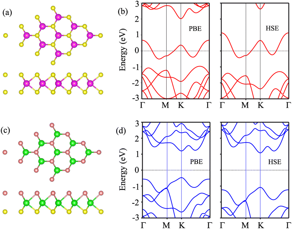
We first examine the atomic and electronic properties of the perfect NbS2 and Janus MoSSe monolayers, as depicted in Fig. 1. Both the Nb2 and Janus MoSSe monolayers show the same hexagonal crystal structure. The lattice constants of NbS2 and Janus MoSSe monolayers are calculated to be 3.32 and 3.28 Å, respectively. These values are in good agreement with the experimental measurements,25,26,51 confirming the reliability of our calculations. The electronic band structures of NbS2 and Janus MoSSe monolayers are illustrated in Fig. 1(b and d). The NbS2 monolayer exhibits metallic behavior, featuring a band that crosses the Fermi level, while Janus MoSSe is a semiconductor with an indirect band gap of 1.67/2.15 eV obtained by using the PBE/HSE functional. Both the maxima of the valence bands and the minima of the conduction bands are located at the K point. It should be noted that the PBE functional underestimates the band gap of 2D materials, whereas the HSE functional provides more accurate results for the band gap. However, due to its low computational cost, the PBE functional is the choice for all calculations.
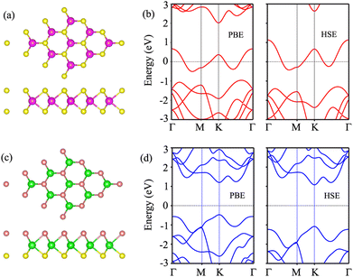 |
| | Fig. 1 Atomic structures of (a) NbS2 and (c) Janus MoSSe monolayers. Yellow, purple, green and brown balls represent the S, Nb, Mo and Se atoms, respectively. Band structures of (b) NbS2 and (d) Janus MoSSe monolayers given by using PBE and HSE functionals. | |
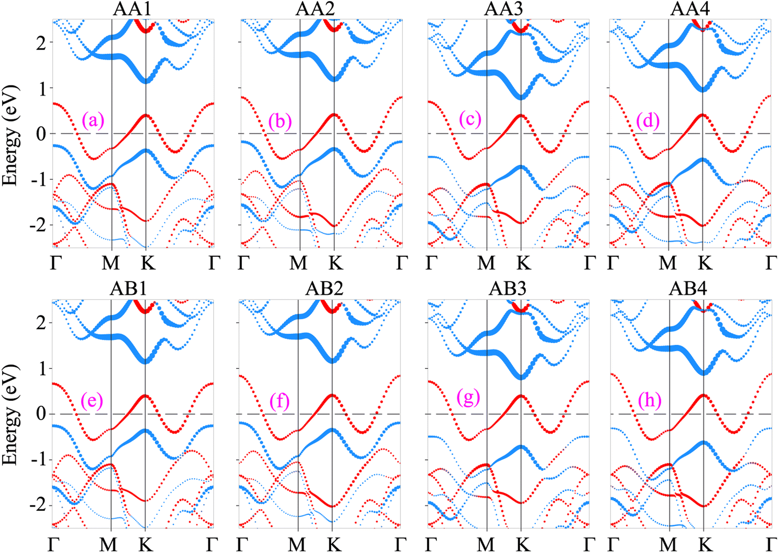
We now build the atomic structure of the NbS2/Janus MoSSe heterostructure for different stacking configurations, as illustrated in Fig. 2. Owing to the small difference in the lattice parameters of NbS2 and Janus MoSSe monolayers, the atomic structure of the NbS2/Janus MoSSe heterostructure consists of a (1 × 1) unit cell of NbS2 and (1 × 1) unit cell of the Janus MoSSe monolayer. The lattice mismatch in the NbS2/Janus MoSSe heterostructure is as small as 0.6%, and it does not significantly affect the main characteristics of the heterostructure. Furthermore, due to the lack of symmetry in the two faces of the Janus MoSSe monolayer, the atomic structures of the NbS2/Janus MoSSe heterostructure split into two main configurations, namely NbS2/SMoSe and NbS2/SeMoS heterostructures. Each NbS2/SMoSe or NbS2/SeMoS heterostructure consists of four different stacking configurations, as presented in Fig. 2. After the geometric optimization, the interlayer distance between the NbS2 and Janus MoSSe layers for each stacking configuration of the NbS2/Janus MoSSe heterostructure is obtained, as listed in Table 1. The AB3 stacking configuration of NbS2/Janus MoSSe has the shortest interlayer distance, while the AA1 stacking configuration shows the largest d. Furthermore, to evaluate the stability of the NbS2/Janus MoSSe heterostructure, we calculate the binding energy (exfoliation energy)52 as follows:
| |  | (1) |
Here,
ENbS2/Janus MoSSe,
ENbS2 and
EJanus MoSSe are the total energies of the NbS
2/Janus MoSSe heterostructure, isolated NbS
2 and Janus MoSSe monolayers, respectively.
A stands for the surface area of the NbS
2/Janus MoSSe heterostructure. The calculated binding energy values obtained from the DFT-D3 method of the NbS
2/Janus MoSSe heterostructure for all eight stacking configurations are in the range from −32 to 20 meV Å
−2, which are listed in
Table 1. Our results show that the binding energy values are of a similar magnitude to those observed in typical van der Waals (vdW) heterostructures, including HfSeX (X = S, Se)/graphene,
53 NbS
2/MoSi
2P
4,
54 MoS
2/MoSSe,
35 MoSSe/g-GeC
55 and GaN/BP.
56 This finding suggests that all stacking configurations of the NbS
2/Janus MoSSe heterostructure exhibit typical vdW interactions. These weak vdW interactions are responsible for maintaining the stability of the heterostructure, which can be synthesized in experiments using various techniques, including chemical vapor deposition (CVD)
39 and epitaxial growth.
57 Additionally, the negative values of the binding energies of the NbS
2/Janus MoSSe heterostructure for all stacking configurations confirm that they are energetically stable. Notably, the AB3 stacking configuration exhibits the lowest binding energy, establishing it as the most energetically stable structure. Additionally, we also used the DFT-D2 method to calculate the binding energy of the NbS
2/MoSSe heterostructure for comparison. One can observe that the DFT-D2 binding energy is larger than that obtained by the DFT-D3 method. However, both DFT-D2 and DFT-D3 consistently predict that the AB3 stacking configuration exhibits the lowest binding energy. Furthermore, to consider the dynamic stability of the AB3 stacking configuration, we further measure its phonon spectrum, as illustrated in Fig. S1 of the ESI.
† We observe that there are no negative frequencies in the phonon spectrum of the AB3 stacking configuration of the NbS
2/Janus MoSSe heterostructure, indicating that such a configuration is dynamically stable. Hence, we focus on this stacking configuration for all the subsequent investigations.
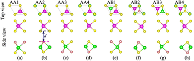 |
| | Fig. 2 Top and side views of the atomic structures of the NbS2/Janus MoSSe heterostructure for different stacking patterns of (a) AA1, (b) AA2, (c) AA3, (d) AA4, (e) AB1, (f) AB2, (g) AB3 and (h) AB4. | |
Table 1 Calculated interlayer distance (d, Å), binding energy calculated by DFT-D3 and DFT-D2 methods (Eb, meV Å−2), Schottky barrier heights (eV), work functions (W, eV) and contact types in the NbS2/Janus MoSSe heterostructure for the different stacking configurations
| Materials |
Stacking types |
d
|
E
b
|
Φ
n
|
Φ
p
|
W
|
Schottky type |
| DFT-D3 |
DFT-D2 |
| NbS2/SMoSe |
AA1 |
3.42 |
−21.50 |
−16.85 |
1.14 |
0.26 |
6.05 |
p-type ShC |
| AA2 |
2.91 |
−20.33 |
−16.84 |
0.78 |
0.51 |
6.11 |
p-type ShC |
| AB1 |
3.34 |
−31.06 |
−28.32 |
1.18 |
0.18 |
6.03 |
p-type ShC |
| AB2 |
2.88 |
−28.15 |
−25.36 |
0.95 |
0.28 |
6.06 |
p-type ShC |
| NbS2/SMoSe |
AA3 |
3.39 |
−21.99 |
−17.03 |
1.14 |
0.25 |
6.07 |
p-type ShC |
| AA4 |
3.31 |
−20.74 |
−17.33 |
0.80 |
0.49 |
6.07 |
p-type ShC |
| AB3 |
2.83 |
−32.74 |
−30.84 |
1.16 |
0.19 |
6.06 |
p-type ShC |
| AB4 |
2.78 |
−30.16 |
−26.54 |
0.89 |
0.31 |
6.08 |
p-type ShC |
The projected band structures of the NbS2/Janus MoSSe heterostructure for all eight stacking configurations are illustrated in Fig. 3. One can find that the electronic band structures of such configurations appear to be a combination of those of the constituent NbS2 and Janus MoSSe monolayers. The nature of such a preservation arises from the dominance of weak van der Waals (vdW) interactions between the NbS2 and Janus MoSSe layers in their corresponding heterostructure. All the stacking configurations of the NbS2/Janus MoSSe heterostructure exhibit metallic behavior with a rough band crossing the Fermi level. By analyzing the projected band structures in Fig. 3, one can observe that a rough band crossing the Fermi level comes from the metallic NbS2 layer. More interestingly, upon the formation of the metal/semiconductor NbS2/Janus MoSSe heterostructure, either an ohmic contact (OhC) or Schottky contact (ShC) is generated, depending on the energy position of the band edges of Janus MoSSe relative to the Fermi level of the NbS2 layer. Hence, comprehending the characteristics of both OhC and ShC contacts plays a crucial role in enabling charge carrier injection and extraction in the metal/semiconductor NbS2/Janus MoSSe heterostructure. From Fig. 3, we can find that all the stacking configurations form a ShC contact because the Fermi level of the metallic NbS2 layer lies between two band edges of semiconductor Janus MoSSe. Based on the Schottky–Mott rule58 the Schottky barriers for n-type and p-type ShC contacts can be established as follows:
and
Here,
EC,
EV and
EF are the CBM and VBM band edges of semiconductor Janus MoSSe and the Fermi level of the metallic NbS
2 layer, respectively. The obtained Schottky barriers for all eight stacking configurations of the NbS
2/Janus MoSSe heterostructure are listed in
Table 1. One can observe that all the stacking configurations of the NbS
2/Janus MoSSe heterostructure exhibit p-type ShC contact with the Schottky barriers ranging from 0.18 to 0.51 eV. The AB3 stacking configuration has the narrowest Schottky barrier compared to other configurations.
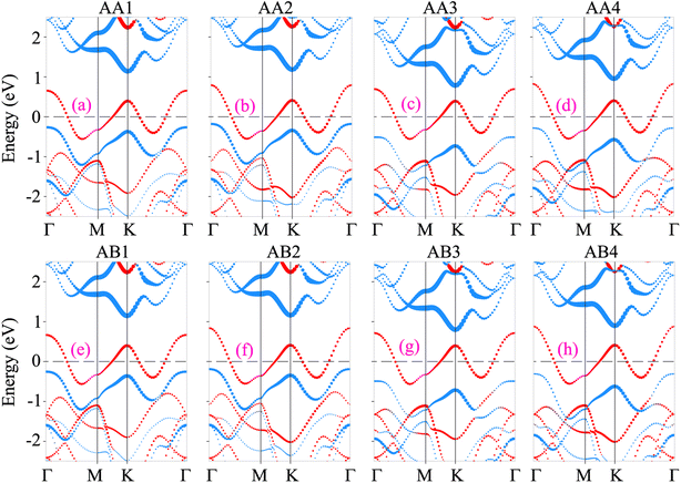 |
| | Fig. 3 Projected band structures of the NbS2/Janus MoSSe heterostructure for different stacking patterns of (a) AA1, (b) AA2, (c) AA3, (d) AA4, (e) AB1, (f) AB2, (g) AB3 and (h) AB4. Red and cyan circles represent the contributions of metallic NbS2 and semiconductor MoSSe layers, respectively. | |
Furthermore, to determine whether the formation of the metal/semiconductor NbS2/Janus MoSSe heterostructure leads to a narrower Schottky barrier compared to the metal/semiconductor NbS2/MoS2 and NbS2/MoSe2 heterostructures, we next calculate the electronic properties of the latter, as depicted in Fig. 4. One can find that all the NbS2/MoS2, NbS2/MoSSe and NbS2/MoSe2 heterostructures form a p-type ShC contact. The Φp Schottky barriers for the NbS2/MoS2, NbS2/MoSSe and NbS2/MoSe2 heterostructures, respectively, are calculated to be 0.32/0.37, 0.18/0.25 and 0.23/0.32 eV by using the PBE/HSE functional. It is clear that the NbS2/Janus MoSSe heterostructure exhibits a narrower Schottky barrier compared to the NbS2/MoS2 and NbS2/MoSe2 heterostructures for both the PBE and HSE prediction. A narrower Schottky barrier results in improved device performance for those based on the metal/semiconductor NbS2/Janus MoSSe heterostructure. These findings illustrate that the Janus MoSSe monolayer can serve as an ideal channel when combined with the 2D metallic NbS2 monolayer, resulting in the formation of a metal/semiconductor NbS2/Janus MoSSe heterostructure that enhances charge carrier injection. Besides, for a more comprehensive understanding of the contributions of each layer in the band structure of the NbS2/Janus MoSSe heterostructure, we plot the partial density states (PDOS) of all atoms in the NbS2/Janus MoSSe heterostructure, as shown in the inset of Fig. 4(a). We can observe that the band crossing the Fermi level is mainly contributed by the Nb-orbitals of the NbS2 layer. Meanwhile, the Mo-orbital states contribute mainly to the CBM of the semiconducting Janus MoSSe layer and its VBM comes from the hybridization between Mo and S atoms in the MoSSe layer. In addition, to evaluate the SOC effect on the electronic properties of the NbS2/MoSSe heterostructure, we further plot its projected band structure with the inclusion of the SOC effect, as depicted in Fig. S2 of the ESI.† It is evident that SOC introduces a split in the valence band of the Janus MoSSe layer at the K point, as illustrated in Fig. S2(b).† However, it is crucial to highlight that despite the split observed in the valence band of the Janus MoSSe layer, this does not lead to a change in the contact type or barrier heights of the NbS2/MoSSe heterostructure because the valence band of the Janus MoSSe layer is located at the Γ point. Hence, the SOC effect has a negligible impact on the electronic properties of the heterostructure.
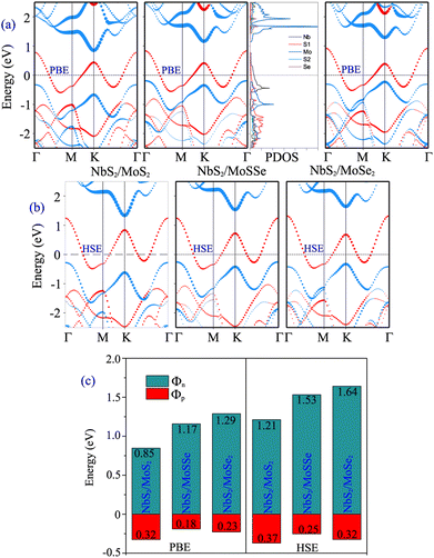 |
| | Fig. 4 Projected band structures of NbS2/MoS2, NbS2/MoSSe and NbS2/MoSe2 heterostructures obtained using (a) PBE and (b) HSE functionals. (c) Schottky barriers of NbS2/MoS2, NbS2/MoSSe and NbS2/MoSe2 heterostructures for the most energetically stable AB3 configuration. The inset presents the partial density of states (PDOS) of all atoms in the NbS2/MoSSe heterostructure for the AB3 stacking configuration. | |
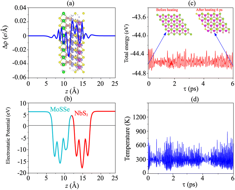
Furthermore, to investigate the charge redistribution at the interface of the NbS2/Janus MoSSe heterostructure, we calculate the charge density difference (CDD) as follows:
| | | Δρ = ρNbS2/MoSSe − ρNbS2 − ρMoSSe | (4) |
Here,
ρNbS2/MoSSe,
ρNbS2 and
ρMoSSe are the charge densities of the NbS
2/MoSSe heterostructure, isolated NbS
2 and Janus MoSSe monolayers, respectively. The CDD at the interface of the NbS
2/MoSSe heterostructure is depicted in
Fig. 5(a). One can find that the electrons are mainly depleted on the side of the NbS
2 layer, while they are mainly accumulated on the side of the Janus MoSSe layer. This finding demonstrates that the electrons are mainly transferred from the NbS
2 to the Janus MoSSe layer. Such charge movement indicates that the metallic NbS
2 layer can be used as contact electrodes for efficient electron injection, with the Janus semiconductor MoSSe layer serving as the channel in field-effect transistors (FETs) based on the NbS
2/MoSSe heterostructure. Bader charge analysis shows that there are only 0.012 electrons, migrating from the NbS
2 to the Janus MoSSe layer. The electrostatic potential of the NbS
2/MoSSe heterostructure is depicted in
Fig. 5(b). It is evident that the NbS
2 layer has a higher potential than the Janus MoSSe layer in the NbS
2/MoSSe heterostructure, confirming that the electrons migrated from the NbS
2 to the MoSSe layer. Furthermore, the charge transfer at the interface of the heterostructure could lead to the formation of an interface dipole, which can change the barrier heights of such a heterostructure. The interface dipole can be obtained as follows:
| | | ΔV = WNbS2 − WNbS2/MoSSe | (5) |
where
WNbS2 and
WNbS2/MoSSe are the work functions of the isolated NbS
2 monolayer and NbS
2/MoSSe heterostructure, respectively. From
Fig. 5(b), the interface dipole at the interface of the NbS
2/MoSSe heterostructure is obtained to be 0.08 eV. In the presence of an interface dipole, the barrier heights of the NbS
2/MoSSe heterostructure can be rewritten as:
and
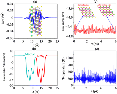 |
| | Fig. 5 (a) Planar averaged charge density difference and (b) electrostatic potential of the NbS2/MoSSe heterostructure for the most energetically stable AB3 configuration. Dark purple and dark pink represent the positive and negative charges, respectively. AIMD simulations of the fluctuation of (c) total energy and (d) temperature as a function of time steps. The insets present the atomic structures of the NbS2/MoSSe heterostructure before and after heating for 6 ps. | |
We observe that the barrier heights of the NbS2/MoSSe heterostructure remain nearly unchanged in the presence of an interface dipole compared to those without it. Such a phenomenon can be attributed to the small magnitude of the interface dipole and the minimal amount of charge transfer.
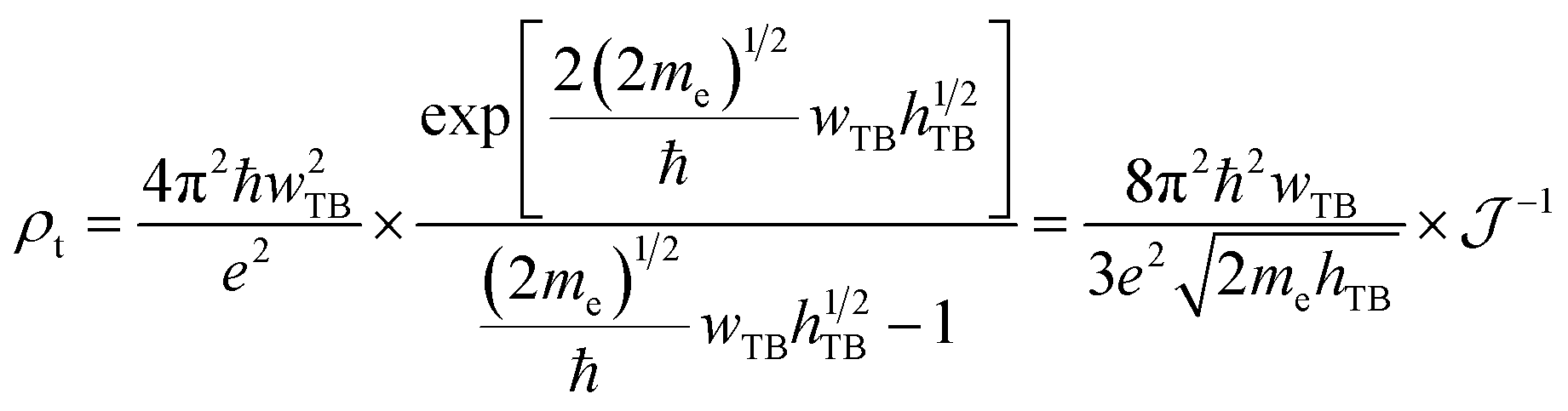
To evaluate the charge injection efficiency of the NbS2/MoSSe heterostructure, we further calculate its tunneling probability  and the tunneling-specific resistivity (ρt) as follows:
| |  | (8) |
and
| |  | (9) |
Here,
hTB and
wTB are the tunneling barrier height and width, respectively. h is the reduced Planck's constant.
e and
me are the electron magnitude and mass of a free electron, respectively. From the electrostatic potential of the NbS
2/MoSSe heterostructure, the
hTB and
wTB are calculated to be 4.61 eV and 1.40 Å, respectively. Using
eqn (8) and
(9), the tunneling probability and tunneling-specific resistivity of the NbS
2/MoSSe heterostructure are 3.23% and 1.89 × 10
−9 Ω cm
2, respectively. Interestingly, the tunneling-specific resistivity of the NbS
2/MoSSe heterostructure is comparable to that observed in other heterostructures, including Bi/MoS
2,
59 Bi, Sb semimetals/TMDs,
60 metal/MSi
2N
4 (M = Mo, W)
61 and 2D (3D) metals/GeSe,
62 suggesting that such a heterostructure could serve as an efficient contact for electronic devices.
Furthermore, to check the thermal stability of the NbS2/MoSSe heterostructure, we perform the ab initio molecular dynamics (AIMD) simulation. The fluctuations of total energy and temperature of the NbS2/MoSSe heterostructure for all stacking configurations as a function of time steps are displayed in Fig. 5(c, d) and S3 of the ESI.† It is evident that the fluctuations of total energy in Fig. 5(c) and S3 of the ESI† are small, and the atomic structures of the NbS2/MoSSe heterostructure for all stacking configurations after heating for 6 ps show no distortion or bond breaking, implying that the NbS2/MoSSe heterostructure is thermally stable at room temperature.
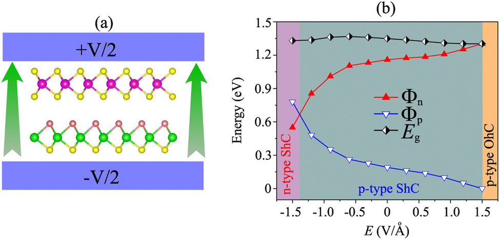
More importantly, the ability to adjust contact characteristics in the NbS2/MoSSe heterostructure is crucial for its applications in next-generation electronic devices. Recently, applying electric fields is considered as an effective way to control both the electronic properties and contact characteristics of 2D heterostructures, such as graphene-based heterostructures63–66 and TMD-based heterostructures.67–70 Therefore, we further investigate the ability to adjust the electronic properties and contact characteristics in the NbS2/MoSSe heterostructure by applying electric fields. The schematic model of applying electric fields along the z direction of the NbS2/MoSSe heterostructure is illustrated in Fig. 6(a). The positive electric field is defined as the direction pointing from the Janus MoSSe to the NbS2 layers. The variation of the Schottky barriers of the NbS2/MoSSe heterostructure under different electric fields is depicted in Fig. 6(b). It is evident that applying an electric field varies the Schottky barriers, resulting in a transformation of the contact types in the NbS2/MoSSe heterostructure. The Φn of the NbS2/MoSSe heterostructure increases as the strength of the electric field increases from −1.5 to +1.5 V Å−1, whereas the Φp had decreased accordingly. This finding implies that the Schottky barriers Φn and Φp change in two opposite directions under the application of electric fields. Under the influence of a negative electric field of −1.3 V Å−1, we observe a reduction in the value of Φn, causing it to become narrower than the Φp of the NbS2/MoSSe heterostructure. This change leads to a shift from p-type ShC to n-type ShC in the NbS2/MoSSe heterostructure. Conversely, when a positive electric field is applied, Φn decreases, yet it remains narrower than the Φp of the heterostructure, maintaining its p-type ShC characteristics. Upon further application of a positive electric field, reaching +1.5 V Å−1, Φn continuously decreases until it reaches zero, signifying a transition from p-type ShC to p-type OhC in the NbS2/MoSSe heterostructure.
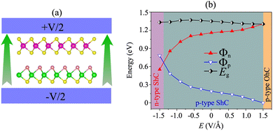 |
| | Fig. 6 (a) The schematic model of an applied electric field along the z direction of the NbS2/MoSSe heterostructure for the most energetically stable AB3 configuration. (b) The variation of the Schottky barriers and contact types in the NbS2/MoSSe heterostructure as a function of electric fields. | |
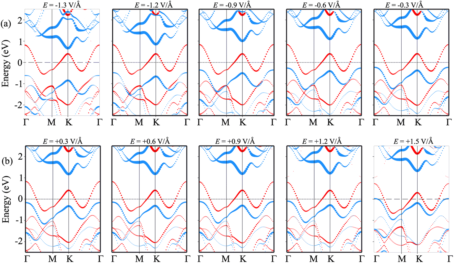
In order to gain deeper insight into the mechanisms underlying the change in the contact barriers and contact types in the NbS2/MoSSe heterostructure, we further plot its projected band structures under different strengths of both negative and positive electric fields, as illustrated in Fig. 7. The impact of a negative electric field is clearly observable on the band edges of the Janus MoSSe semiconductor. Specifically, the VBM of the Janus MoSSe semiconductor shifts to a lower binding energy, moving further away from the Fermi level. In contrast, the CBM shifts to a lower binding energy but moves closer to the Fermi level. Hence, the application of a negative electric field causes a decrease in the Φn and an increase in the Φp. Under a negative electric field of −1.3 V Å−1, the CBM of the Janus MoSSe semiconductor is positioned closer to the Fermi level than its VBM, suggesting that the NbS2/MoSSe heterostructure is transformed from p-type ShC into n-type ShC. Likewise, the application of a positive electric field induces shifts in the band edges of the Janus MoSSe monolayer, although in different directions compared to a negative electric field. The VBM of the semiconducting MoSSe layer shifts closer to the Fermi level, while its CBM moves farther away from the Fermi level. Hence, under the application of a positive electric field, the VBM of the Janus MoSSe semiconductor is always positioned closer to the Fermi level than the CBM, indicating that the NbS2/MoSSe heterostructure maintains the p-type ShC characteristics. With a further increase in the positive electric field, the VBM of the Janus MoSSe layer continues to shift towards the Fermi level and eventually crosses the Fermi level at a positive electric field strength of +1.5 V Å−1. This finding demonstrates that a positive electric field results in a transformation from ShC into OhC in the NbS2/MoSSe heterostructure. Indeed, it's important to note that the transition from ShC to OhC in the metal/semiconductor heterostructure is a critical factor that plays a pivotal role in enhancing the performance of devices built based on the NbS2/MoSSe heterostructure. For instance, with the application of a positive electric field of +1.5 V Å−1, the tunneling-specific resistivity of the NbS2/Janus MoSSe heterostructure reduces to 0.82 × 10⁻⁹ Ω cm2. Hence, this transformation can have a profound impact on device characteristics and is a key consideration for optimizing device functionality and efficiency.
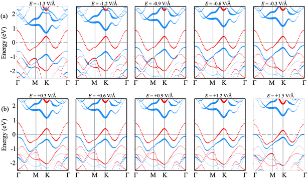 |
| | Fig. 7 Projected band structures of the metal/semiconductor NbS2/MoSSe heterostructure for the most energetically stable AB3 configuration under different strengths of (a) negative and (b) positive electric fields. Red and blue lines represent the contributions of the metallic NbS2 and semiconducting MoSSe layers, respectively. | |
4 Conclusions
In summary, we have designed a metal/semiconductor NbS2/MoSSe heterostructure and systematically investigated its electronic properties and the formation of contact types using first-principles calculations. The NbS2/MoSSe heterostructure exhibits exceptional structural and thermal stability, making it a compelling candidate for practical applications. The NbS2/MoSSe heterostructure manifests p-type Schottky contacts characterized by small Schottky barriers and low tunneling resistance, signifying its substantial utility in electronic device integration. Furthermore, we found that the electronic properties, contact barriers, and contact types within this heterostructure can be controlled by manipulating the stacking configurations and applying external electric fields. Notably, negative electric fields facilitate a transition from p-type Schottky to n-type Schottky contacts, whereas positive electric fields induce a shift from Schottky to ohmic contacts. These findings offer valuable theoretical insights for exploiting the NbS2/MoSSe heterostructure's versatility in advancing nanoelectronic and optoelectronic device development.
Conflicts of interest
There are no conflicts to declare.
References
- A. Zavabeti, A. Jannat, L. Zhong, A. A. Haidry, Z. Yao and J. Z. Ou, Nano-Micro Lett., 2020, 12, 1–34 CrossRef PubMed.
- P. Miró, M. Audiffred and T. Heine, Chem. Soc. Rev., 2014, 43, 6537–6554 RSC.
- S. Z. Butler, S. M. Hollen, L. Cao, Y. Cui, J. A. Gupta, H. R. Gutiérrez, T. F. Heinz, S. S. Hong, J. Huang and A. F. Ismach,
et al.
, ACS Nano, 2013, 7, 2898–2926 CrossRef CAS PubMed.
- K. S. Novoselov, A. K. Geim, S. V. Morozov, D.-e. Jiang, Y. Zhang, S. V. Dubonos, I. V. Grigorieva and A. A. Firsov, Science, 2004, 306, 666–669 CrossRef CAS PubMed.
- S. Manzeli, D. Ovchinnikov, D. Pasquier, O. V. Yazyev and A. Kis, Nat. Rev. Mater., 2017, 2, 1–15 Search PubMed.
- R. Yang, Y. Fan, Y. Zhang, L. Mei, R. Zhu, J. Qin, J. Hu, Z. Chen, Y. Hau Ng and D. Voiry,
et al.
, Angew. Chem., Int. Ed., 2023, 62, e202218016 CrossRef CAS PubMed.
- Y. Wei, P. Zhang, R. A. Soomro, Q. Zhu and B. Xu, Adv. Mater., 2021, 33, 2103148 CrossRef CAS PubMed.
- S. Abdolhosseinzadeh, X. Jiang, H. Zhang, J. Qiu and C. J. Zhang, Mater. Today, 2021, 48, 214–240 CrossRef CAS.
- W. Meng, X. Liu, H. Song, Y. Xie, X. Shi, M. Dargusch, Z.-G. Chen, Z. Tang and S. Lu, Nano Today, 2021, 40, 101273 CrossRef CAS.
- H. Shi, Y. Dong, S. Zheng, C. Dong and Z.-S. Wu, Nanoscale Adv., 2020, 2, 4212–4219 RSC.
- Y.-L. Hong, Z. Liu, L. Wang, T. Zhou, W. Ma, C. Xu, S. Feng, L. Chen, M.-L. Chen and D.-M. Sun,
et al.
, Science, 2020, 369, 670–674 CrossRef CAS PubMed.
- Y. Yin, Q. Gong, M. Yi and W. Guo, Adv. Funct. Mater., 2023, 33, 2214050 CrossRef CAS.
- Q. Wang, L. Cao, S.-J. Liang, W. Wu, G. Wang, C. H. Lee, W. L. Ong, H. Y. Yang, L. K. Ang and S. A. Yang,
et al.
, npj 2D Mater. Appl., 2021, 5, 71 CrossRef CAS.
- C. Liu, H. Chen, S. Wang, Q. Liu, Y.-G. Jiang, D. W. Zhang, M. Liu and P. Zhou, Nat. Nanotechnol., 2020, 15, 545–557 CrossRef CAS PubMed.
- L. Hu, B. J. Kim, S. Ji, J. Hong, A. K. Katiyar and J.-H. Ahn, Appl. Phys. Rev., 2022, 9, 041308 CAS.
- S. Conti, G. Calabrese, K. Parvez, L. Pimpolari, F. Pieri, G. Iannaccone, C. Casiraghi and G. Fiori, Nat. Rev. Mater., 2023, 1–17 Search PubMed.
- H. Xiang, Y.-C. Chien, Y. Shi and K.-W. Ang, Small Struct., 2022, 3, 2200060 CrossRef.
- Q. H. Wang, K. Kalantar-Zadeh, A. Kis, J. N. Coleman and M. S. Strano, Nat. Nanotechnol., 2012, 7, 699–712 CrossRef CAS PubMed.
- M. Wu, Y. Xiao, Y. Zeng, Y. Zhou, X. Zeng, L. Zhang and W. Liao, InfoMat, 2021, 3, 362–396 CrossRef CAS.
- X. Duan, J. Xu, Z. Wei, J. Ma, S. Guo, H. Liu and S. Dou, Small Methods, 2017, 1, 1700156 CrossRef.
- Z. Zhang, P. Yang, M. Hong, S. Jiang, G. Zhao, J. Shi, Q. Xie and Y. Zhang, Nanotechnology, 2019, 30, 182002 CrossRef CAS PubMed.
- T. Kang, T. W. Tang, B. Pan, H. Liu, K. Zhang and Z. Luo, ACS Mater. Au, 2022, 2, 665–685 CrossRef CAS PubMed.
- Q. Wang, Y. Lei, Y. Wang, Y. Liu, C. Song, J. Zeng, Y. Song, X. Duan, D. Wang and Y. Li, Energy Environ. Sci., 2020, 13, 1593–1616 RSC.
- P. A. L. Sino, L.-Y. Feng, R. A. B. Villaos, H. N. Cruzado, Z.-Q. Huang, C.-H. Hsu and F.-C. Chuang, Nanoscale Adv., 2021, 3, 6608–6616 RSC.
- A.-Y. Lu, H. Zhu, J. Xiao, C.-P. Chuu, Y. Han, M.-H. Chiu, C.-C. Cheng, C.-W. Yang, K.-H. Wei and Y. Yang,
et al.
, Nat. Nanotechnol., 2017, 12, 744–749 CrossRef CAS PubMed.
- J. Zhang, S. Jia, I. Kholmanov, L. Dong, D. Er, W. Chen, H. Guo, Z. Jin, V. B. Shenoy and L. Shi,
et al.
, ACS Nano, 2017, 11, 8192–8198 CrossRef CAS PubMed.
- A. C. Riis-Jensen, M. Pandey and K. S. Thygesen, J. Phys. Chem. C, 2018, 122, 24520–24526 CrossRef CAS.
- L. Dong, J. Lou and V. B. Shenoy, ACS Nano, 2017, 11, 8242–8248 CrossRef CAS PubMed.
- W.-J. Yin, B. Wen, G.-Z. Nie, X.-L. Wei and L.-M. Liu, J. Mater. Chem. C, 2018, 6, 1693–1700 RSC.
- Y.-N. Wen, M.-G. Xia and S.-L. Zhang, Comput. Mater. Sci., 2018, 152, 20–27 CrossRef CAS.
- C. Long, Y. Dai and H. Jin, Phys. Rev. B, 2021, 104, 125306 CrossRef CAS.
- J. Yuan, Y. Shan and T. Li, J. Phys. D: Appl. Phys., 2020, 53, 125502 CrossRef CAS.
- C. Jin, X. Tang, X. Tan, S. C. Smith, Y. Dai and L. Kou, J. Mater. Chem. A, 2019, 7, 1099–1106 RSC.
- X. Lei, C. Ouyang and K. Huang, Appl. Surf. Sci., 2021, 537, 147919 CrossRef CAS.
- A. Singh, M. Jain and S. Bhattacharya, Nanoscale Adv., 2021, 3, 2837–2845 RSC.
- C. Shang, X. Lei, B. Hou, M. Wu, B. Xu, G. Liu and C. Ouyang, J. Phys. Chem. C, 2018, 122, 23899–23909 CrossRef CAS.
- A. Castellanos-Gomez, X. Duan, Z. Fei, H. R. Gutierrez, Y. Huang, X. Huang, J. Quereda, Q. Qian, E. Sutter and P. Sutter, Nat. Rev. Methods Primers, 2022, 2, 58 CrossRef CAS.
- S.-J. Liang, B. Cheng, X. Cui and F. Miao, Adv. Mater., 2020, 32, 1903800 CrossRef CAS PubMed.
- Q. Fu, X. Wang, J. Zhou, J. Xia, Q. Zeng, D. Lv, C. Zhu, X. Wang, Y. Shen and X. Li,
et al.
, Chem. Mater., 2018, 30, 4001–4007 CrossRef CAS.
- J. Tan, S. Li, B. Liu and H.-M. Cheng, Small Struct., 2021, 2, 2000093 CrossRef CAS.
- D. M. Seo, J.-H. Lee, S. Lee, J. Seo, C. Park, J. Nam, Y. Park, S. Jin, S. Srivastava and M. Kumar,
et al.
, ACS Photonics, 2019, 6, 1379–1386 CrossRef CAS.
- J. Hafner, J. Comput. Chem., 2008, 29, 2044–2078 CrossRef CAS PubMed.
- G. Kresse and J. Furthmüller, Phys. Rev. B: Condens. Matter Mater. Phys., 1996, 54, 11169 CrossRef CAS PubMed.
- J. P. Perdew, K. Burke and M. Ernzerhof, Phys. Rev. Lett., 1996, 77, 3865 CrossRef CAS PubMed.
- J. P. Perdew, K. Burke and M. Ernzerhof, Phys. Rev. Lett., 1998, 80, 891 CrossRef CAS.
- G. Kresse and D. Joubert, Phys. Rev. B: Condens. Matter Mater. Phys., 1999, 59, 1758 CrossRef CAS.
- S. Grimme, J. Comput. Chem., 2004, 25, 1463–1473 CrossRef CAS PubMed.
- S. Grimme, J. Comput. Chem., 2006, 27, 1787–1799 CrossRef CAS PubMed.
- J. Heyd and G. E. Scuseria, J. Chem. Phys., 2004, 121, 1187–1192 CrossRef CAS PubMed.
- J. Heyd, J. E. Peralta, G. E. Scuseria and R. L. Martin, J. Chem. Phys., 2005, 123, 174101 CrossRef PubMed.
- P. Zhang, C. Bian, J. Ye, N. Cheng, X. Wang, H. Jiang, Y. Wei, Y. Zhang, Y. Du and L. Bao,
et al.
, Sci. China Mater., 2020, 1548–1559 CrossRef CAS.
- S. R. Tavares, P. I. R. Moraes, R. B. Capaz and A. A. Leitao, Appl. Surf. Sci., 2019, 483, 762–771 CrossRef CAS.
- Q. Luo, S. Yin, X. Sun, G. Guo and X. Dai, Diamond Relat. Mater., 2022, 128, 109223 CrossRef CAS.
- Z. Li, J. Han, S. Cao and Z. Zhang, Appl. Surf. Sci., 2023, 157766 CrossRef CAS.
- Y.-L. Liu, Y. Shi and C.-L. Yang, Appl. Surf. Sci., 2021, 545, 148952 CrossRef CAS.
- H. Shu, M. Zhao and M. Sun, ACS Appl. Nano Mater., 2019, 2, 6482–6491 CrossRef CAS.
- Y. Gong, J. Lin, X. Wang, G. Shi, S. Lei, Z. Lin, X. Zou, G. Ye, R. Vajtai and B. I. Yakobson,
et al.
, Nat. Mater., 2014, 13, 1135–1142 CrossRef CAS PubMed.
- J. Bardeen, Phys. Rev., 1947, 71, 717 CrossRef.
- P.-C. Shen, C. Su, Y. Lin, A.-S. Chou, C.-C. Cheng, J.-H. Park, M.-H. Chiu, A.-Y. Lu, H.-L. Tang and M. M. Tavakoli,
et al.
, Nature, 2021, 593, 211–217 CrossRef CAS PubMed.
- T. Su, Y. Li, Q. Wang, W. Zhao, L. Cao and Y. S. Ang, J. Phys. D: Appl. Phys., 2023, 56, 234001 CrossRef.
- C. C. Tho, C. Yu, Q. Tang, Q. Wang, T. Su, Z. Feng, Q. Wu, C. Nguyen, W.-L. Ong and S.-J. Liang,
et al.
, Adv. Mater. Interfaces, 2023, 10, 2370006 CrossRef.
- L. Cao, X. Deng, Z. Tang, G. Zhou and Y. S. Ang, Appl. Phys. Lett., 2022, 121, 113104 CrossRef CAS.
- X. Gong, G. Yuan, X. Ma, H. Lv, F. Zhang, J. He and W. Zou, Diamond Relat. Mater., 2022, 128, 109206 CrossRef CAS.
- W. Xiong, C. Xia, X. Zhao, T. Wang and Y. Jia, Carbon, 2016, 109, 737–746 CrossRef CAS.
- X. Ma, H. Bo, X. Gong, G. Yuan, Z. Peng, J. Lu and Q. Xie, Appl. Surf. Sci., 2023, 615, 156385 CrossRef CAS.
- X. Yan, I. S. Esqueda, J. Ma, J. Tice and H. Wang, Appl. Phys. Lett., 2018, 112, 032101 CrossRef.
- Q. Peng, C. Si, J. Zhou and Z. Sun, Appl. Surf. Sci., 2019, 480, 199–204 CrossRef CAS.
- W. Li, T. Wang, X. Dai, Y. Ma and Y. Tang, J. Alloys Compd., 2017, 705, 486–491 CrossRef CAS.
- Y. Feng, H. Bai, M. An, Y. Wu and X. Wang, ACS Appl. Nano Mater., 2023, 6, 5795–15806 Search PubMed.
- X. Li, G. Jia, J. Du, X. Song, C. Xia, Z. Wei and J. Li, J. Mater. Chem. C, 2018, 6, 10010–10019 RSC.
|
| This journal is © The Royal Society of Chemistry 2024 |
Click here to see how this site uses Cookies. View our privacy policy here. 
 Open Access Article
 This Open Access Article is licensed under a
  cd,
Huynh V.
Phuc
cd,
Huynh V.
Phuc


 and the tunneling-specific resistivity (ρt) as follows: