
 Open Access Article
 This Open Access Article is licensed under a
 Creative Commons Attribution 3.0 Unported Licence
Embedding Pd into SnO2 drastically enhances gas sensing†
Katarzyna
Jabłczyńska
 ab,
Alexander
Gogos
cd,
Christian M. P.
Kubsch
a and
Sotiris E.
Pratsinis
*a
ab,
Alexander
Gogos
cd,
Christian M. P.
Kubsch
a and
Sotiris E.
Pratsinis
*a
aParticle Technology Laboratory, Institute of Energy and Process Engineering, Department of Mechanical and Process Engineering, ETH Zurich, CH-8092 Zurich, Switzerland. E-mail: pratsinis@ethz.ch
bFaculty of Chemical and Process Engineering, Warsaw University of Technology, 00-645 Warsaw, Poland
cParticles-Biology Interactions, Department of Materials Meet Life, Swiss Federal Laboratories for Materials Science and Technology (Empa), CH-9014 St. Gallen, Switzerland
dNanoparticle Systems Engineering Laboratory, Institute of Energy and Process Engineering, Department of Mechanical and Process Engineering, ETH Zurich, CH-8092 Zurich, Switzerland
First published on 31st January 2024
Abstract
Combustion aerosol processes can uniquely embed noble metals into semiconducting particles. Here, monocrystalline SnO2 particles embedded with Pd and/or PdOx were made by flame spray pyrolysis (FSP) of appropriate precursors through microexplosions by droplet-to-particle conversion as the crystal size was proportional to the cube root of precursor solution concentration, C. These particles were air-annealed and leached with nitric acid for removal of metallic Pd from their surface. The SnO2 crystal size varied from 11 to 24 nm and was in close agreement with the primary particle size determined by nitrogen adsorption. The embedded fraction of Pd ranged from about 30 to 80% of the nominal Pd-content. This was achieved by judiciously varying the C, Pd content and the ratio of precursor solution to dispersion oxygen flowrates during FSP. The response of sensors made by doctor blading films of such particles to 1 ppm of acetone and CO was evaluated at 350 °C and 50% relative humidity. Embedding Pd/PdOx into SnO2 significantly increased the sensor response: 2–6 times over that of pure or conventionally-made Pd-containing SnO2 sensors at low nominal Pd-contents (0.2 mol%). For higher ones (i.e. 1 mol% Pd), the sensor response was enhanced by up to two orders of magnitude. This is attributed to Pd atoms in the SnO2 lattice near the particle surface and/or Pd/PdOx clusters acting as nanoelectrodes into SnO2 films and altering their transducing properties as shown by high resolution electron microscopy, XPS and baseline resistance measurements of pure and Pd-embedded SnO2 sensing films.
Introduction
Gas sensors are used widely for detection of drunk driving and monitoring compliance of automotive emissions as well as to prevent gas explosions and poisoning in mines. Due to their low cost and portability, they are most promising for monitoring air quality outdoors (e.g. NO2)1 or indoors (e.g. formaldehyde),2 food quality (e.g. methanol in alcoholic beverages),3 for medical diagnostics (e.g. diabetes or inflammatory markers such as NO for asthma)4 or monitoring fat-burning from breath acetone.5 What links these applications is the requirement to selectively measure very low, sometimes at few ppb, concentrations of specific analytes. Therefore, there is a clear need for highly sensitive materials driving the search of new chemical compositions and novel material structures (or morphologies).Standard chemiresistive gas sensors consist of a functional film of semiconducting nanoparticles, deposited between a pair of electrodes. When that film is exposed to analyte gas it serves as the catalyst for the reaction between adsorbed oxygen species and analyte on the film surface.6 This reaction alters the concentration of charge carriers in the film and can be measured as a change of its resistance. Therefore, a good sensor, among other features, should give the highest possible response, i.e. a change in resistance in relation to the baseline in clean air.
Tin oxide is the most common gas sensor. Doping it with noble metals (NM) is frequently used to enhance its sensitivity.7 In contrast to most methods for preparation of SnO2 with NM (impregnation,8 reverse micelles,9 ball mill mixing10 and photodeposition11) in which SnO2 particles are only externally decorated with NM clusters, flame spray pyrolysis (FSP) uniquely allows placing NM on the surface and inside the sensing nanoparticles.12 Recently it was shown that solely embedding palladium (Pd) or PdO into SnO2 increased significantly the sensor response to CO, acetone and ethanol over that from pure and Pd-decorated SnO2 made, for example, by Pd photodeposition.13
Here, this discovery is explored systematically by varying the embedded Pd-content and SnO2 crystal size by closely controlling the FSP synthesis of such particles. Palladium is removed from the surface of SnO2 by leaching and the effect of embedded Pd fraction on sensor response to 1 ppm of inorganic (CO) and organic vapors (acetone) at 350 °C and 50% relative humidity is investigated focusing on the sensitivity of such materials as their selectivity can be enhanced readily by filters.14 Potential mechanisms for the observed drastic increase of sensor response to both analytes due to Pd embedding are assessed revealing the role of Pd near the SnO2 surface and Pd/PdOx domains into its bulk.
As our focus is on understanding the partitioning of Pd between the surface and interior of SnO2 and the subsequent impact on gas sensing, we benchmarked the sensitivity, the most basic property of gas sensors, at a commonly employed temperature, humidity and concentration of acetone and CO. Other sensor characteristics such as selectivity, stability and response and recovery times have not been investigated as they largely follow those of pure and Pd-containing SnO2 sensors. The effect of sensing temperature, humidity and analyte concentration on the performance of SnO2-based sensors has been documented extensively for acetone13,15–18 and CO11,16,19–22 as summarized in Table S1 in the ESI.†
Experimental
Synthesis of sensing nanoparticles
Pure and Pd-doped SnO2 particles were prepared by FSP.13 A precursor solution of tin(II)-ethylhexanoate (Aldrich, purity >92.5%) and palladium(II)-acetylacetonate (Aldrich, purity ≥99%) in xylene (Aldrich, purity >96%) with a total metal ion (or precursor solution) concentration, C, of 0.1, 0.5, 1.0 or 1.5 M was used. Palladium was added at the concentration of 0, 0.1, 0.2, 0.5, 1 and 3 mol% of total metal content. This solution was fed to the capillary of a concentric spray nozzle at 1, 5 and 9 ml min−1 by a syringe pump and dispersed by an annular oxygen flow of 2, 5 or 8 l min−1. A premixed methane/oxygen (1.3/3.2 l min−1) flame ignited and supported the spray flame. A circular sheath oxygen flow of 5 l min−1 was used around that flame to assure complete combustion of the precursor. The FSP inlet conditions for all experiments are listed in Table S2 in the ESI.†Using a vacuum pump, the powder was collected (Busch, Seco SV 1025C) on a glass-fiber filter (GF6 Albet-Hahnemuehle, 257 mm diameter) 50 cm above the burner. Product powders were scraped off the filter surface with a spatula and sieved with 0.25 mm stainless steel sieve to remove filter fragments. A portion of all powders was annealed in air at 500 °C for 5 hours (Carbolite Gero, Gero 30–3000 °C). Both as-prepared and annealed powders were kept for further characterization.
Removal of surface Pd
First, 150 mg of annealed powder were placed in a quartz reactor tube and secured with glass wool on both ends. The powder was then reduced by passing 100 ml min−1 of 5% H2 in Ar for 30 min at 150 °C. Then 100 mg of such reduced powder was placed inside a round bottom flask where 85 ml of ultrapure water (Merck Millipore) and 15 ml of nitric acid (65% HNO3 in water, purity ≥99.99%) were added. Then the flask was heated up to 60 °C in an oil bath and stirred under reflux for 4 h at 500 rpm to dissolve the palladium on the surface of SnO2 particles.13 Then the flask contents were transferred to falcon tubes and the particles were separated from solution by centrifugation (7200 of relative centrifugal force for 10 min), washed thrice with ultrapure water and dried in a vacuum oven (SalvisLAB, Vacucenter) at 50 °C and 50 mbar for 12 h. The resulting leached solution was analyzed with inductively coupled plasma-optical emission spectroscopy (ICP-OES, Agilent 5110) to determine the amount of leached Pd. The ICP-OES was calibrated using standards for Sn and Pd in HNO3 solutions (inorganic ventures). The surface palladium fraction was defined as the ratio of the measured amount of leached palladium and the nominal Pd content in the powder. The SnO2 powders with Pd content 0, 0.1, 0.3 and 0.5 mol% were completely digested by adding 3 ml concentrated HNO3 (69%) and 500 μL HF (40%) and heating to 240 °C for 10 min in a pressurized microwave (UltraClave, MLS GmbH). Digestion was performed both on annealed and leached powders to determine the total and embedded Pd content. After digestion, samples were filled up to 50 ml with ultrapure water. The concentrations of Sn and Pd ions then were measured by ICP-OES (Agilent 5110) as the above leached solutions.Particle characterization
Particle phase composition and crystal size, d, were obtained by X-ray diffraction (XRD, Bruker D2 Phaser) at 40 kV and 40 mA at 2θ (Cu Kα) of 20–70° with a step size of 0.1° and scanning speed of 0.0972° s−1. The patterns and crystal size were determined by Rietveld fundamental parameter refinement with the Topaz 4.2 software (Bruker) using the characteristic parameters of cassiterite SnO2 (PDF 41-1445) and Pd (PDF 01-1310) and PdO (PDF 43-1024).The specific surface area (SSA) and surface equivalent particle diameter (dBET) of the powders were measured by 5-point N2 adsorption at 77 K (Micromeritics Tristar II Plus) using the Brunauer–Emmett–Teller method. Powder samples were degassed under N2 at 150 °C for 1.5 h prior the adsorption measurement. The dBET was calculated using the densities of SnO2 (6.95 g cm−3) and PdO (8.3 g cm−3).
Specimens for transmission electron microscopy were prepared by dispersing a spatula tip of dry powder in 500 μL of high purity ethanol (>99.9%, LiChrosolv, Supelco) in an agate mortar. A volume of 10 μL of supernatant from the mortar was then drawn through a lacey carbon TEM grid (EM resolutions) using a tissue. Then, the grid was washed thrice with ultrapure water and air dried. High-angle annular dark-field scanning transmission electron microscopy (HAADF-STEM) images and energy-dispersive X-ray (EDXS) elemental maps were then obtained from these specimens using a FEI Talos (F200X, Super-X EDS, 4 detector configuration, FEI, Hillsboro, OR, USA).
X-ray Photoelectron Spectroscopy (XPS) measurements were conducted on samples of as-prepared, annealed and leached powders containing 1 and 3 mol% of Pd, as for that with 0.2 mol% Pd, the signal to noise ratio was too low for analysis. Powders were compressed into separate indium foil pieces and subjected to analysis using a Quantum 2000 XPS system (Physical Electronics). Detailed descriptions of these measurements can be found in the ESI.† Literature binding energies for relevant Pd species along with respective average, min/max and standard deviation values that were used to constrain the curve fitting model are shown in Table S3, ESI.†
Sensor assembly and measurements
Powders were mixed with 1,2-propanediol (Sigma-Aldrich, purity >> 99%) to form viscous and homogeneous pastes. The pastes were doctor bladed13 with a razor on Al2O3 sensor substrates (Electronic Design Center, Case Western Reserve University, Electrode type #103) having two interdigitated Pt electrodes (sputtered, 350 μm width and spacing) on the front and a Pt heater on the back. The sides of the substrates were secured with 15 μm thick aluminum foil to control the thickness of the spread film. The sensors were dried at room temperature for 4 hours, followed by 16 hours at 80 °C. Finally, the sensors were annealed for 30 minutes at 300 °C with 10 °C min−1 ramping to improve mechanical stability of the film and remove any remains of organics used during paste preparation. An illustration depicting the sensor, outlining the measurement principle of film resistance (R) and demonstrating the doctor-blading procedure can be found in Fig. S1 and S2, respectively, within the ESI.†The sensor was placed in a closed chamber and heated to 350 °C by DC through its substrate Pt heater, adjusted by linear regression for temperature and the resistance was determined individually for each sensor using thermocamera (Fluke, Ti110). A synthetic air stream of 1 l min−1 and 50% relative humidity (RH) was continuously passed through the chamber with the sensor until a stable baseline resistance (Rair) was achieved. The humidity was tuned by mixing a stream of dry synthetic air with an equal stream of air saturated with water vapor in an inline water-filled bubbler. To measure sensor response to analytes, acetone or carbon monoxide was admixed to the air stream from calibrated gas standards in an appropriate amount to result in a concentration of 1 ppm. The sensor exposure to analyte lasted for, at least, 10 minutes to ensure that resistance has reached a final value (Ranalyte). The interval between two consecutive pulses was, at least, 20 minutes to ensure the resistance returned to the baseline. The sensor response (S) is:
 | (1) |
Results and discussion
SnO2 crystal size control
Fig. 1 shows the as-prepared (open symbols) and annealed (filled symbols) SnO2 crystal size, d, as a function of the FSP precursor solution concentration, C, for pure (squares) and doped SnO2 with 0.2 (triangles) and 1 mol% Pd (circles) made with the ratio of precursor solution flowrate (P, ml min−1) to dispersion O2 flowrate (D, l min−1), P/D = 5/5. Increasing C enlarges the SnO2 crystals. In contrast, the Pd content had no effect on the as-prepared SnO2 crystals that increased from 5.6–5.8 nm to 13.4–14.2 nm with C increasing from 0.1 to 1.5 M. In contrast, increasing the Pd content hindered the growth of annealed SnO2 by the solute drag effect24 as shown also in Fig. S3 in the ESI† in agreement with Pineau et al.13 Given that the particle size as determined by N2 adsorption (Fig. S3, ESI,† squares) was close to the crystal size (Fig. S3, ESI,† circles) at all Pd contents for both as-prepared and annealed particles, monocrystalline SnO2 particles were made here.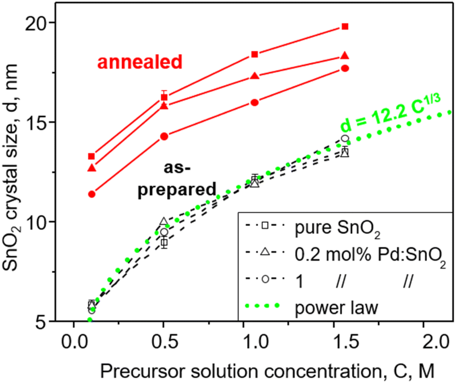 | ||
| Fig. 1 Crystal size of as-prepared (black, open symbols) and annealed (red, filled symbols) pure (squares) and doped SnO2 with 0.2 (triangles) and 1 mol% Pd (circles) made at FSP precursor solution flowrate, P (ml min−1), to dispersion O2 flowrate, D (l min−1), of 5/5 as a function of FSP precursor solution concentration (C). | ||
Most interestingly, the size of all as-prepared particles followed a power law (Fig. 1, dotted line) with C, d = 12.2C1/3, indicating that particle size directly relates to precursor solution concentration, C, and consequently to formation from single droplets by evaporation-precipitation.25 Most likely, such droplets were formed by microexplosions.26 So SnO2 formation takes place largely by droplet-to-particle conversion at the highly oxidic conditions of spray combustion.
Increasing the ratio of FSP precursor solution to dispersion O2 flowrate, P/D, increases the precursor aerosol concentration and flame temperature (Fig. S4 in the ESI†) that increase SnO2 crystal size (Fig. S5, ESI†) as seen in Fig. 1 with increasing C. However, the increased flame temperature at high P/D results in slightly larger SnO2 crystals, i.e. 12 nm at P/D = 5/5 (Fig. 1) and 15 nm at P/D = 5/2 for pure SnO2 (Fig. S5, ESI†). It should be noted that the SnO2 crystal size did not change much due to reduction with H2, leaching and subsequent washing and drying.
Palladium distribution and oxidation state
Metallic Pd can be leached from the SnO2 surface as shown for photodeposited Pd onto SnO2, where more than 99% of the nominal Pd content was removed.13 For flame-made particles, the question arises regarding the partition of Pd between the particle's surface and interior, as well as its oxidation state. All annealed Pd/SnO2 particles were leached with HNO3 to remove Pd from the SnO2 surface and determine the Pd surface fraction from the Pd ion concentration in the leachate and subsequently the embedded fraction of the total Pd content. To confirm results from HNO3 leaching, Pd/SnO2 powders with Pd content ranging from 0.1 to 0.5% of Pd were completely digested using HF. Digestion was performed before and after leaching to determine the total Pd and the embedded Pd content. Solutions remaining after HF digestion were diluted and the concentrations of Sn and Pd ions were measured by ICP-OES.Juxtaposition of the results of HNO3 leaching and HF digestion experiments is shown in Fig. S6 in the ESI.† The sum of Pd determined in the leachates and that in the residual material after leaching was close to 100% of the nominal Pd content in the SnO2 powder for all Pd-contents.
To investigate the impact of FSP process conditions on the embedded content of Pd, one FSP process variable (precursor concentration, C, precursor solution/dispersion O2 flowrate ratio, P/D, or Pd content, Pd%) was varied while the other two were kept constant. For example, the fraction of embedded Pd into SnO2 from total (nominal) Pd contents of 0.1, 0.2, 0.5, 1 and 3 mol% produced at C = 0.5 M and P/D = 5/5 is shown as a function of SnO2 crystal size in Fig. 2 (squares). Increasing the total Pd content, drastically decreases the embedded Pd fraction from 73 to 35% as the actual amount of embedded Pd increases into SnO2 since the total Pd content in SnO2 increases (Fig. S7 in the ESI†).
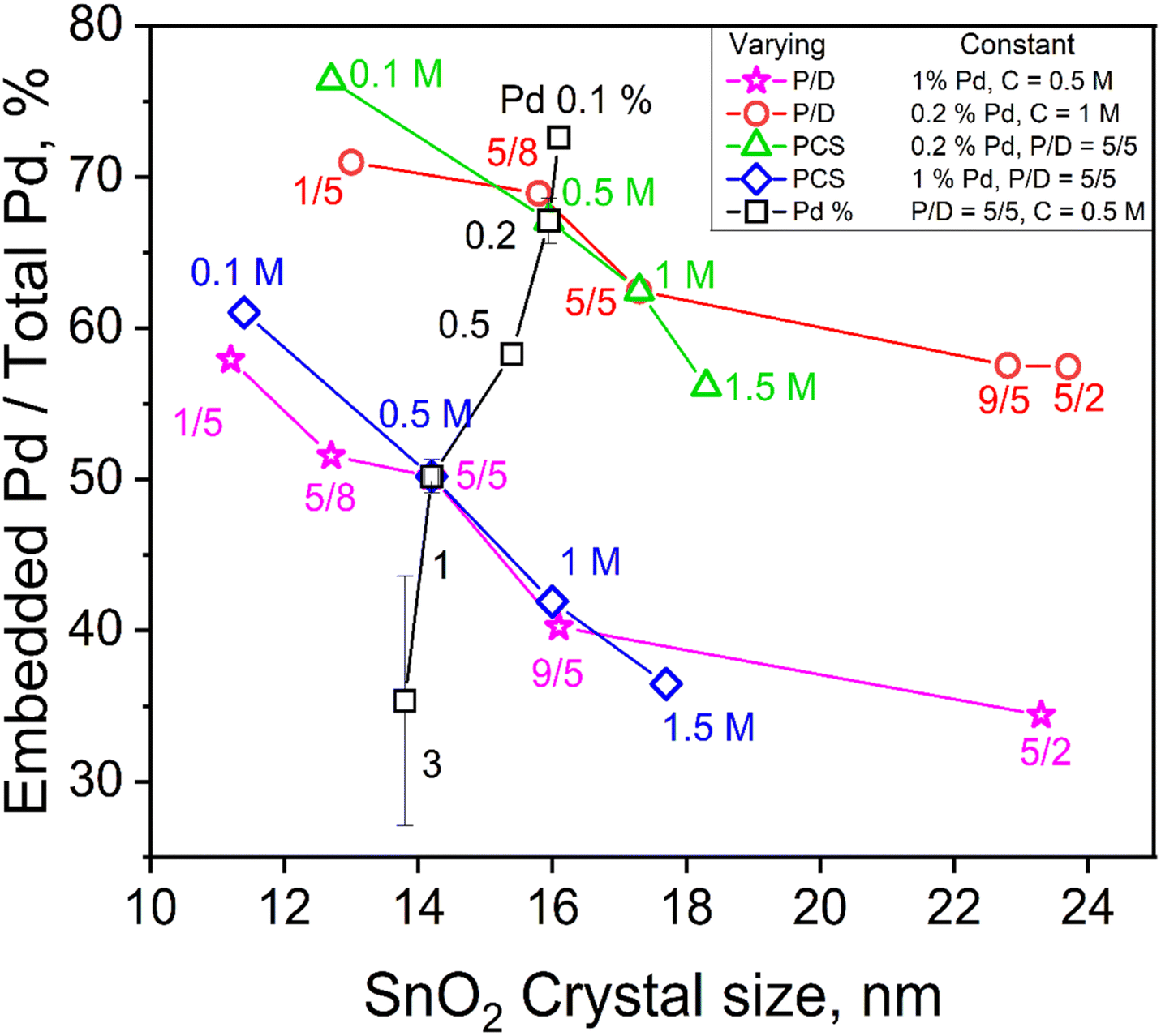 | ||
| Fig. 2 The embedded Pd fraction as a function of SnO2 crystal size in the annealed powders made by varying one of the FSP process variables, P/D (stars and circles), C (diamonds and triangles) or Pd content (squares), while keeping the other two constant. The actual embedded Pd content (mol%) as a function crystal size is provided in Fig. S7 in the ESI.† | ||
Increasing the C from 0.1 to 1.5 (Fig. 2, triangles) and P/D from 1/5 to 5/2 (circles) at 0.2 mol% nominal Pd content hardly altered the mole fraction of embedded Pd in SnO2 (Fig. S7 in the ESI†), even though the embedded fraction decreased from 76 to 56% of the nominal value. The same increase of C (Fig. 2, diamonds) and P/D (stars) at higher Pd content, 1 mol%, decreased the embedded fraction of Pd from 60 to 35% as both FSP variables increase SnO2 crystal size while inversely affect the flame temperature (Fig. S4 in the ESI†) indicating its limited significance at the employed conditions. As SnO2 particles are formed by droplet-to-powder conversion (Fig. 1), the precursor solution concentration, C, largely determines their size. Precursor solutions of increasing C and/or P/D increase the metal ion concentration and form larger SnO2 crystals (Fig. 1 and S7 in the ESI†). As particle formation takes place within microdroplets26 (Fig. 1), Pd and Sn are well mixed there and embedding of Pd species into the SnO2 matrix takes place.
To visualize the change in content and dispersion of Pd in and/or on the particles at different Pd doping levels, STEM-EDXS mapping was used. Fig. 3 presents EDXS elemental maps of annealed SnO2 doped with various amounts of Pd (a) before and (b) after leaching with nitric acid. The change of particle Pd content can be observed on the basis of the respective image EDXS spectrum shown in the lower panel of Fig. 3a. As the Pd content increases from 0 to 3%, the relative height of the characteristic Pd-Lα peak at 2.839 keV increases as well. Even though there is no Pd peak in the EDXS spectrum of pure SnO2 (0 mol% Pd, Fig. 3a), it still appears on the elemental map above. The Pd map in this case is only based on unspecific Bremsstrahlung X-ray counts, generated once material is within the path of the electron beam. The exact spectrum for the different Pd map areas for pure SnO2 in Fig. S8cd in the ESI† proves that there is no detectable Pd in this sample. Before leaching, pure SnO2 (0% Pd in Fig. 3a) showed the characteristic Sn Lλ peak at 3.045 keV and was free from Pd Lα X-ray counts at 2.839 keV. Using a high beam current of 8 nA, Pd down to 0.2 mol% was detected at 2.839 keV of the EDX spectrum. At the lowest Pd-contents of 0.2 & 0.5 mol%, virtually no Pd clusters were visible while still a distinct Pd peak could be seen at 2.839 keV. This suggests that Pd is distributed inside and/or on the surface of SnO2 – atomically dispersed or in Pd clusters close to or below ≈2 nm in diameter (LOD).
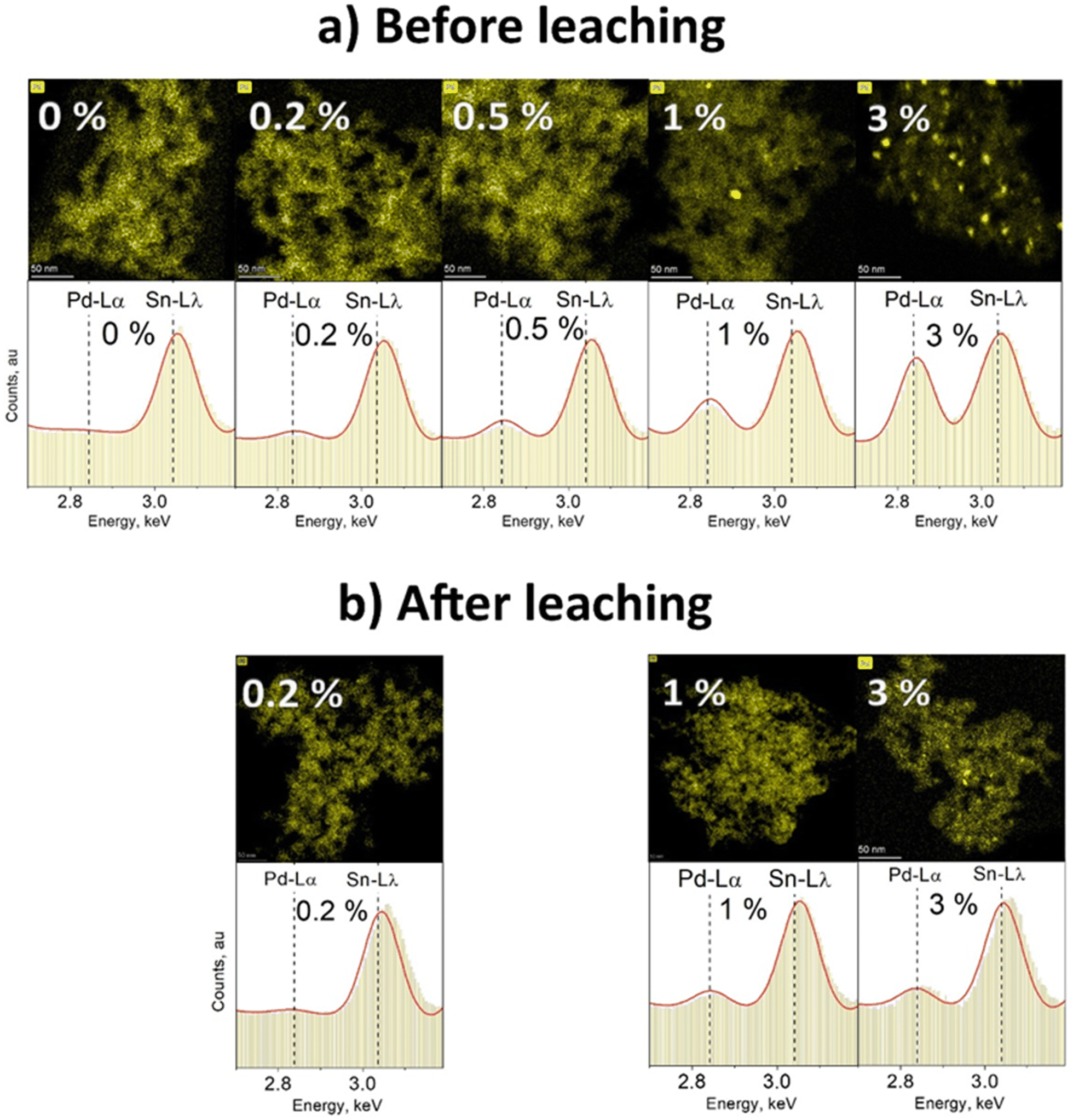 | ||
| Fig. 3 (a) Top panel: Pd elemental maps of annealed SnO2 doped with Pd contents of 0, 0.2, 0.5, 1 & 3 mol% and made at C = 0.5 M, P/D = 5/5. Bottom panel: EDXS spectra corresponding to the image area above. All images were recorded at the same imaging conditions (450 kx magnification, beam current of 8 nA, 10 frames at 50 μs dwell time). As the content of Pd increases, more and larger Pd-rich (bright) spots are visible. (b) Top panel: Pd elemental maps of SnO2 containing originally 0.2, 1 & 3 mol% Pd after undergoing leaching with HNO3. Only in the 3 mol% sample some Pd-rich spots are visible. The bottom panel: EDXS spectra corresponding to the image area above. Clearly, the amount of Pd in relation to Sn has decreased compared to these samples before leaching and corresponds to the embedded Pd into SnO2. | ||
In the elemental map for SnO2 containing 1 mol% Pd before leaching (Fig. 3a), single Pd clusters larger than 2 nm can be seen. Also for 3 mol% Pd before leaching (Fig. 3a) even more Pd-rich spots with a diameter from a few to a dozen nm can be observed. These observations are in line with Koziej et al. for impregnated27 Pd and Gschwend et al. for photodeposited11 Pd onto SnO2. Using K-edge XANES & EXAFS, for example, Koziej et al.27 found that at low Pd-contents, e.g. 0.2 mol%, Pd is finely dispersed and does not form any clusters which only become apparent at high Pd concentrations (3 mol%).
After leaching, no Pd clusters were detected for 0.2 mol% Pd (as expected) and hardly any for 1 mol% Pd (Fig. 3b). When comparing the latter to its initial sample, we go from some to virtually no clusters, indicating that most of the Pd clusters were actually on the SnO2 particle surface. However, when 3 mol% Pd/SnO2 was leached, still some Pd clusters were visible. Their number and average size were smaller than before leaching, but still single clusters up to 10 nm in diameter were present. Such clusters could be embedded in SnO2 which would protect them from the HNO3 leaching. Another possibility is that such visible Pd-rich regions are not clusters, but only superficially Pd-enriched SnO2 areas that were in contact with larger Pd clusters prior to their leaching. Such enrichment might be caused by annealing-induced solid-state diffusion of Pd into SnO2 and/or solid-state reaction13 forming PdSnOx. This is supported by the fact that the fraction of leachable Pd decreases by 20–40% after annealing.13
Clearly very small amounts of Pd can be incorporated into SnO2 by FSP that could form solid solutions. Such atomic Pd doping should occur only to a limited extent as the SnO2 diffraction patterns were not affected by Pd at all Pd contents employed here (Fig. S9 and S10 in the ESI†). However, with increased Pd loading, Pd forms a separate phase (i.e. Pd/PdOx) that cannot be detected by XRD. This phase resulted in domains and clusters into and onto the SnO2 proportional in size and number to the nominal Pd content as shown in Fig. 3a. Larger clusters are not easily embedded in SnO2. As a result, more Pd would be exposed to leaching, decreasing the embedded Pd fraction at higher nominal Pd loadings (i.e. only 35% is embedded at the 3 mol% nominal Pd loading, Fig. 2).
To more closely investigate the oxidation states of Pd, X-ray Photoelectron Spectroscopy (XPS) analysis was performed (Fig. S11†). Due to the limited depth of analysis (typically ≈1–5 nm),28,29 this technique provides valuable information about the surface and near-surface regions rather than the bulk of the SnO2 powder. Detailed spectra with deconvolution into individual oxidation states are presented in the ESI, Fig. S12 and S13.† They revealed the dominating presence of oxidized forms (PdOx) of palladium as well as metallic Pd0 in all the as-prepared and annealed (unleached and leached) samples (Fig. S14 in the ESI†).
The measurements showed PdOx![[thin space (1/6-em)]](https://www.rsc.org/images/entities/char_2009.gif) :Pd0 ratios of ≈1.1 and ≈0.7 for particles containing 1 and 3 mol% of Pd, respectively, for both as-prepared and annealed samples (Fig. S15, ESI†). These are consistent with Deligiannakis et al.30 who found a PdOx:Pd0 of 0.8 for FSP-made Pd/TiO2. As the boiling point of metallic palladium is 2963 °C and the decomposition temperature of palladium oxide is around 800 °C,31 palladium clusters formed in high temperatures regions of the flame will possess a metallic character. However, as these clusters reach temperatures of around 700 °C away from the flame, they undergo oxidation32 but only at the surface layer which has access to oxygen. The Pd clusters core and portion incorporated into SnO2, lacking access to oxygen, would remain in their metallic form as confirmed by the XPS spectra.
:Pd0 ratios of ≈1.1 and ≈0.7 for particles containing 1 and 3 mol% of Pd, respectively, for both as-prepared and annealed samples (Fig. S15, ESI†). These are consistent with Deligiannakis et al.30 who found a PdOx:Pd0 of 0.8 for FSP-made Pd/TiO2. As the boiling point of metallic palladium is 2963 °C and the decomposition temperature of palladium oxide is around 800 °C,31 palladium clusters formed in high temperatures regions of the flame will possess a metallic character. However, as these clusters reach temperatures of around 700 °C away from the flame, they undergo oxidation32 but only at the surface layer which has access to oxygen. The Pd clusters core and portion incorporated into SnO2, lacking access to oxygen, would remain in their metallic form as confirmed by the XPS spectra.
After leaching however, the PdOx:Pd0 ratio increased dramatically to 2.2 and 2.8 for 1 mol% and 3 mol% initial Pd, respectively (Fig. S15, ESI†) suggesting a lower content in metallic Pd after leaching. In this case, it was possible to remove all Pd from the surface, suggesting surface only Pd can be fully reduced to Pd0 after the reduction process, as only Pd0 is soluble in HNO3.11 However, in this study, Pd was introduced already in the flame and thus mixed into the entirety (inside and outside) of the SnO2 particles. Therefore, here, it is possible that – as suggested from XPS – a portion of metallic Pd can remain shielded beneath a protective PdOx/SnO2 surface.
In a first line, the XPS results demonstrate that the particle surface is dominated by oxidized Pd species. However, they also suggest the presence of metallic Pd, most likely near the surface. Whether this is true and valid also for deeper layers of the particles warrants further investigation by complementary and bulk analysis techniques such as X-ray absorption spectroscopy.
Sensing performance
To investigate the impact of embedded Pd on the sensing of organics (acetone) and inorganics (CO), the response of SnO2 sensors containing (a) embedded and surface Pd, (b) only embedded and (c) only surface Pd was compared. Fig. 4 shows the sensor response to 1 ppm of acetone at 350 °C in 50% RH by pure (green diamonds) and 0.2 mol% Pd-doped SnO2 (an optimal Pd content33,34 for gas sensors) as a function of SnO2 crystal size made at various P/D at C = 1 M (circles in Fig. 2).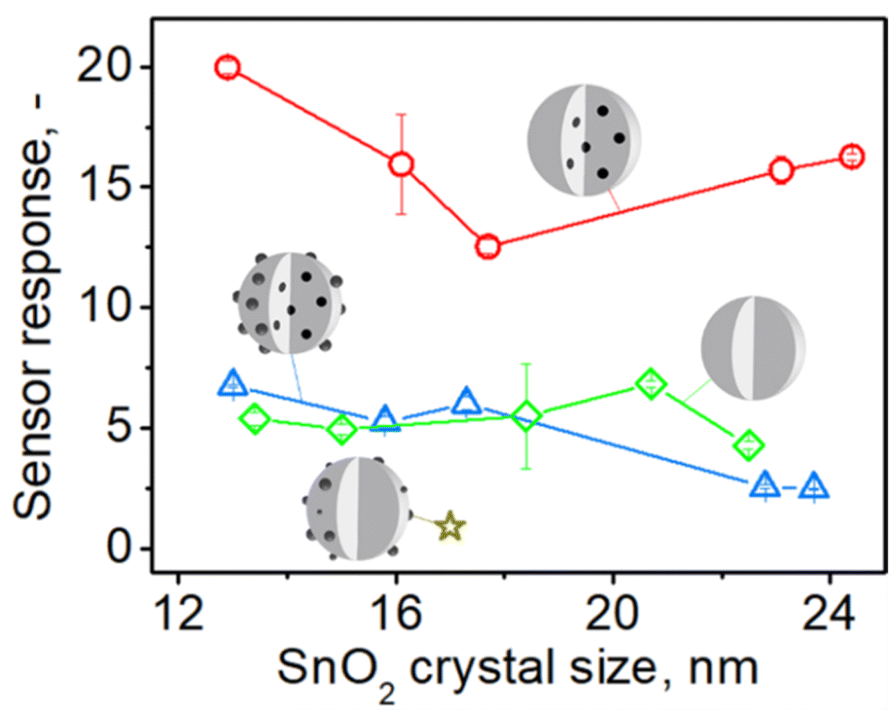 | ||
| Fig. 4 The response to 1 ppm of acetone at 350 °C in 50% RH by sensors made with pure (green diamonds) and 0.2 mol% Pd-containing SnO2 particles before (blue triangles) and after HNO3 solution leaching and removal of surface Pd (red circles) made at various FSP precursor solution to dispersion O2 flowrate ratio (starting from the left P/D = 1/5, 5/8, 5/5, 9/5, 5/2) and C = 1 M as a function of SnO2 crystal size. The star shows the response of a SnO2 sensor that contained 0.2 mol% photodeposited Pd.11 Schematics of sensing particles depict with gray the SnO2 and black the Pd/PdOx atoms, clusters or domains. | ||
For all sensors, increasing the P/D and the resulting SnO2 crystal size from 13 to 24 nm (Fig. S5 in the ESI†) hardly affects their response consistent with Güntner et al.12 Pure SnO2 sensors had a stronger response (green diamonds) than those containing only surface Pd (gold star)11 but comparable to those having both surface and embedded Pd (blue triangles). However, when surface Pd was removed from the SnO2 particles, their response (red circles) increases by 2 to 6 times over pure (diamonds) and Pd-containing SnO2 (triangles) that had 50% more Pd, regardless of SnO2 crystal size.
These observations are attributed to the detrimental effect of surface Pd (Fig. 4, gold star) and the enhancement of sensing provided by embedded Pd, as depicted in Fig. 4 (red circles), which is fully manifested only after removal of surface Pd. If the sensing reaction takes place mostly locally at the surface of noble metal clusters, no electron transfer to the conduction band of SnO2 will occur and thus no change in the conductivity of the sensing film.35 Therefore, it is commonly observed that sensors exhibit a maximum response when there is only a small amount of dopant present, as sensitivity decreases with increasing dopant content. For SnO2 containing both surface and internal palladium (Fig. 4, triangles), it is plausible that their effects mutually negate each other.
When the same sensors were tested towards 1 ppm of CO at the same conditions (Fig. S16 in the ESI†), the response for all sensors again was hardly affected by SnO2 crystal size12 from 13 to 23 nm. The response of the pure SnO2 sensors (green diamonds) is lower or comparable to that containing both fractions of Pd (blue triangles). Again, when the surface Pd is removed, the sensor response (red circles) increases 2–6 times over that of pure SnO2 (green diamonds) and that containing both surface and embedded Pd (blue triangles).
To better understand this enhancement, sensors with high nominal palladium loading of 1% (or 0.6 to 0.4 mol% actual embedded Pd, Fig. S7 in the ESI†) made at increasing precursor solution concentrations C (and subsequently particle size from 11 to 18 nm, Fig. 1) were tested towards acetone at the same conditions as above (Fig. 5). Sensors containing only surface Pd (gold star) or both surface and embedded Pd (blue triangles) showed hardly any response to 1 ppm of acetone and well below that of pure SnO2 (green diamonds). When, however, surface Pd is removed, their response (red circles) becomes 14 to 95 times higher. This response is also higher or comparable to that of pure SnO2 (green square and diamonds). Nevertheless, please note that the best of these responses is 3–5 times lower than that of sensors containing 0.2 mol% Pd (Fig. 4). This is consistent with the literature showing that sensors with low Pd contents (0.1–0.2 mol%) exhibit higher response than those with higher Pd loadings (0.5–3 mol% Pd).9,11,33,36
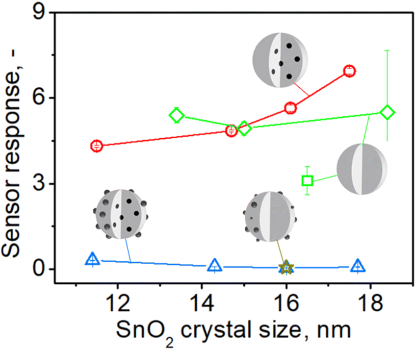 | ||
| Fig. 5 The response to 1 ppm of acetone at 350 °C in 50% RH by pure (green square,13 diamonds – responses from Fig. 4) and 1 mol% Pd-containing SnO2 sensors before (blue triangles) and after leaching and removal of surface Pd (red circles) made at various FSP precursor solution concentrations (starting from the left C = 0.1, 0.5, 1, 1.5 M) and i/D = 5/5 as a function of SnO2 crystal size. The star shows the response of a sensor that contained 1 mol% photodeposited Pd onto SnO2 particles by FSP at C = 0.5 M and same P/D.11 | ||
When the above sensors were exposed to 1 ppm of CO (Fig. S17 in the ESI†), they gave similar results: hardly any response by those containing surface and embedded Pd (blue triangles), which is lower than that of pure SnO2 (green square and diamonds) and a much higher response by the sensor containing only embedded Pd (red circles) that reached a 125-fold amplification for the largest – 18 nm – SnO2 crystals (C = 1.5 M). The response of these sensors was also 2–3 times lower than that for 0.2 mol% Pd-doped sensors, similar to acetone (Fig. 4). Response times of about 10 seconds for pure SnO2 sensors were observed and a moderate increase to 20–40 seconds for those containing 0.2% Pd before its surface removal, in agreement with literature.11 Notably, leaching of surface Pd halved the response times to those before leaching. Recovery times of approximately 40–125 seconds were observed for pure SnO2 and 30 to 200 seconds for Pd-containing SnO2.
To better understand the sensing mechanism of embedded Pd, the baseline of pure and Pd-containing SnO2 sensor was examined before and after leaching surface Pd from the latter ones (Fig. 6). The resistance of films containing 0.2 mol% Pd (surface and embedded, blue triangles) was about an order of magnitude higher than pure SnO2 (green squares) in agreement with Korotcenkov et al.33 This can be attributed to the presence of palladium oxide clusters on the surface. A similar picture holds also for sensors made with 1 mol% Pd (Fig. S18 in the ESI†). As mentioned before, there are two oxidation states of Pd, and thus both PdO and PdO2 can form surface clusters. The PdO2 is metallic while PdO, of which a significant fraction (up to 50%, Fig. S14, ESI,†) is found on/near the surface of the particles according to XPS measurements, is a p-type semiconductor.37 Band bending at binary and ternary heterojunctions with n-type SnO2 causes transfer of electrons and extension of the depletion layer and thus increases the film resistance.
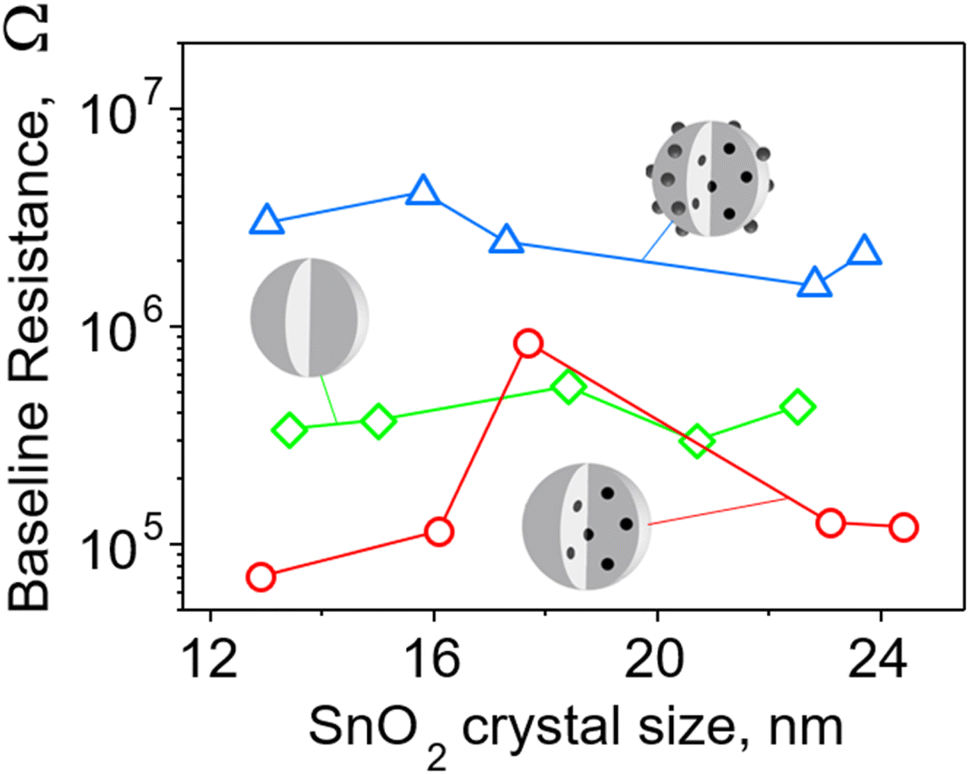 | ||
| Fig. 6 Baseline resistance of pure and 0.2 mol% Pd-doped SnO2 films as a function of SnO2 crystal size for particles made at various P/D (Fig. 4). Films of nanoparticles doped with Pd (blue triangles) both on the surface and in the bulk have the highest resistance – almost an order of magnitude higher than that of pure SnO2 film (green diamonds). Most films of nanoparticles with only embedded Pd (red circles) have resistance significantly lower than the other two SnO2 films. | ||
When the surface Pd was removed, the film resistance fell even below that of pure SnO2 in all except one case (Fig. 6, red circles). This indicates that embedded Pd improves the conductive properties of the film possibly due to the shift of the Fermi level and/or the existence of nanoelectrodes.38 When Pd is dispersed at the atomic level within the crystalline lattice of SnO2, the electronic structure is likely to be changed through introduction of additional energy levels arising from defects in the crystalline structure introduced by dopant atoms.39 The atomically dispersed Pd within the SnO2 lattice has the potential to induce defects, such as oxygen vacancies, which are recognized as the primary source of n-type conductivity in40 SnO2 or Pd-related defects. Such defects can serve as charge carriers, increasing the material's conductivity and enhancing its response to analytes.6 The introduction of additional energy levels originating from defects can raise the position of the Fermi level to a higher energy, approaching the conduction band. This would facilitate the promotion of electrons to the conduction band, creating more free charge carriers (electrons) available for conduction and lowering the baseline resistance of the sensing film.
For SnO2 doped with 1 and 3 mol% Pd we also encounter Pd clusters with a diameter of a few nanometers. These are located within the SnO2 particle (Fig. 3b). It is presumed that the presence of embedded Pd or PdO domains can establish efficient conduction pathways within the film, thus minimizing its electrical resistance.38
Embedding Pd into the SnO2 bulk allows for synthesis of sensors characterized by both low resistance and high response, because there are no surface Pd clusters to compete chemically with SnO2. Embedded Pd clearly improves the transducing properties of the sensing film.
Alternatively, the observed increase in sensor response after leaching may be attributed to imparting specific surface properties to the material through the removal of external Pd clusters, which distinguish it from pure SnO2. These properties predominantly refer to increased surface catalytic activity. A similar technique to the leaching method employed in our study, aimed at removing surface-decorating metal clusters, was utilized by Yang and Flytzani-Stephanopoulos et al. to obtain single atoms of gold on CeO2 catalyst surfaces by treating them with a solution of NaCN.41 This treatment effectively eliminated the majority of metallic Au, leaving behind cationic Au atoms that formed strong bonds with CeO2 changing the surface properties of the catalyst. Similarly, in our investigation, the leaching selectively eliminates surface Pd clusters while allowing atomically dispersed Pd ions to remain within the SnO2 lattice, affecting surface activity similarly to single atom catalysts.41–43 As have been seen from XPS analysis (Fig. S14, ESI,†), the near-surface region of the particles still contained oxidized and metallic Pd. The Pd ions within the SnO2 lattice can provide initial adsorption sites for analyte molecules offering free valences and, by that, lowering their energy barrier of adsorption.27 Single Pd ions directly activate lattice oxygen which is not reactive at the pure SnO2 surface.44,45
Conclusions
Tin oxide particles embedded with Pd were prepared by flame spray pyrolysis (FSP) of appropriate precursors followed by annealing and leaching metallic Pd from the surface of these particles with nitric acid. The SnO2 crystal size and the embedded fraction of Pd inside SnO2 were closely controlled by varying the FSP precursor solution concentration (C), total Pd content and the ratio of precursor solution (ml min−1) to dispersion oxygen (l min−1) flowrate (P/D). The response of sensors made with nominal Pd content of 0.2 and 1 mol% obtained at varying C and P/D was tested towards 1 ppm of acetone and carbon oxide (CO) at 350 °C and 50% relative humidity. The SnO2 crystal size increased with increasing C and P/D, while it decreased slightly with increasing Pd content. That way, SnO2 crystals in the range of 11–24 nm were obtained with the embedded palladium fraction ranging from about 20% to almost 76% of the nominal Pd content. As shown by Scanning Transmission Electron Microscopy (STEM) and Energy Dispersive X-ray Analysis (EDXS), at contents of 0.5 mol% and below, palladium was homogeneously dispersed within and/or on SnO2. Palladium domains and clusters smaller than 10 nm are visible at higher Pd contents, e.g. 1 and 3 mol%.The SnO2 crystal size hardly affected the sensor response in the employed size range. The removal of surface palladium from 0.2 mol% Pd-doped SnO2 significantly enhanced (2–6 times) the sensor response to CO and acetone over that of pure SnO2 sensors and those containing both surface and embedded Pd and greatly exceeds (17–33 times) the response of SnO2 with the same nominal content (0.2 mol%) of photodeposited Pd. At high nominal Pd content, i.e. 1 mol%, the response of SnO2 sensors merely embedded with Pd is from one to two orders of magnitude higher than those containing both surface and embedded Pd.
This drastic enhancement of sensor response can be attributed to Pd atoms in the SnO2 lattice that may change charge carrier concentration and therefore conductance and responsiveness of the film. Also Pd atoms on/near the SnO2 particle surface can lower the adsorption energy of analytes while Pd/PdO clusters may act as nanoelectrodes enhancing the transducing properties of the sensing film.
Author contributions
S. E. P. conceived the study. K. J. established and ran the experimental studies, evaluated analysis and proposed interpretation. C. M. P. K. assisted with the experiments. A. G. carried out the microscopic and XPS data analyses and proposed interpretations. K. J. and S. E. P. wrote the manuscript. All authors have given approval to the final version of the manuscript.Conflicts of interest
There are no conflicts to declare.Acknowledgements
This research was funded by the Particle Technology Laboratory, ETH Zurich and the Swiss National Science Foundation (#175754 and 182668 and R'Equip 170729). We acknowledge the Scientific Center for Optical and Electron Microscopy (ScopeM) of the ETH Zurich for providing access to their microscopes. Also, we like to thank Mr Erik Mayr at EMPA Dübendorf for conducting the XPS measurements and Dr Patrick Rupper at EMPA St. Gallen for fruitful XPS discussions.References
- G. Sberveglieri, S. Groppell and G. Coccoli, Sens. Actuators, 1988, 15, 235–242, DOI:10.1016/0250-6874(88)87013-6.
- J. A. Dirksen, K. Duval and T. A. Ring, Sens. Actuators, A, 2001, 80, 106–115, DOI:10.1016/S0925-4005(01)00898-X.
- S. Abegg, L. Magro, J. van den Broek, S. E. Pratsinis and A. T. Güntner, Nat. Food, 2020, 1, 351–354, DOI:10.1038/s43016-020-0095-9.
- A. T. Güntner, S. Abegg, K. Königstein, P. A. Gerber, A. Schmidt-Trucksäss and S. E. Pratsinis, ACS Sens., 2019, 4, 268–280, DOI:10.1021/acssensors.8b00937.
- A. T. Güntner, N. A. Sievi, S. J. Theodore, T. Gulich, M. Kohler and S. E. Pratsinis, Anal. Chem., 2017, 89, 10578–10584, DOI:10.1021/acs.analchem.7b02843.
- D. Degler, U. Weimar and N. Barsan, ACS Sens., 2019, 4, 2228–2249, DOI:10.1021/acssensors.9b00975.
- N. Yamazoe, Y. Kurokawa and T. Seiyama, Sens. Actuators, 1983, 4, 283–289, DOI:10.1016/0250-6874(83)85034-3.
- S. Matsushima, T. Maekawa, J. Tamaki, N. Miura and N. Yamazoe, Chem. Lett., 1989, 18, 845–848, DOI:10.1246/cl.1989.845.
- M. Yuasa, T. Masaki, T. Kida, K. Shimanoe and N. Yamazoe, Sens. Actuators, B, 2009, 136, 99–104, DOI:10.1016/j.snb.2008.11.022.
- H. Yoshiyama, S. Tanaka, Y. Mikami, S. Ohshio, J. Ni-shiura, H. Kawakami, H. Kobayashi, J. Cryst, H. Kasano, K. Megumi, H. Yamamoto, J. G. Duh, J. W. Jou and B. S. Chiou, J. Electrochem. Soc., 1989, 136, 2740–2747, DOI:10.1149/1.2097581.
- P. M. Gschwend, F. M. Schenk, A. Gogos and S. E. Pratsinis, Materials, 2021, 14, 5921–5934, DOI:10.3390/ma14205921.
- A. T. Güntner, N. J. Pineau and S. E. Pratsinis, Prog. Energy Combust. Sci., 2022, 90, 100992–101030, DOI:10.1016/j.pecs.2022.100992.
- N. J. Pineau, S. D. Keller, A. T. Güntner and S. E. Pratsinis, Microchim. Acta, 2020, 187, 96–105, DOI:10.1007/s00604-019-4080-7.
- J. van den Broek, I. C. Weber, A. T. Güntner and S. E. Pratsinis, Mater. Horiz., 2021, 8, 661–684, 10.1039/D0MH01453B.
- H. Wang, Y. Qu, Y. Li, H. Chen and Z. Lin, J. Nanosci. Nanotechnol., 2013, 13, 1858–1862, DOI:10.1166/jnn.2013.7131.
- M. Epifani, J. Arbiol, E. Pellicer, E. Comini, P. Sicilian, G. Faglia and J. R. Morante, Cryst. Growth Des., 2008, 8, 1774–1778, DOI:10.1021/cg700970d.
- S. Shao S, H. Wu, S. Wang, Q. Hong, R. Koehn, T. Wu and W. F. Rao, J. Mater. Chem. C, 2015, 3, 10819–10829, 10.1039/c5tc02188j.
- F. I. Shaikh, L. P. Chikhale, I. S. Mulla and S. S. Suryavanshi, Ceram. Int., 2017, 43, 10307–10315, DOI:10.1016/j.ceramint.2017.05.060.
- Y. Chen, H. Qin and J. Hu, Appl. Surf. Sci., 2018, 428, 207–217, DOI:10.1016/j.apsusc.2017.08.205.
- X. T. Yin and X. M. Guo, Sens. Actuators, B, 2014, 200, 213–218, DOI:10.1016/j.snb.2014.04.026.
- P. Kutukov, M. Rumyantseva, V. Krivetskiy, D. Filatova, M. Batuk, J. Hadermann, N. Khmelevsky, A. Aksenenko and A. Gaskov, Nanomaterials, 2018, 8, 917, DOI:10.3390/nano8110917.
- N. Barsan, L. Mädler and U. Weimar, In Proceedings of the Nanosensing: Materials, Devices, and Systems III, SPIE, 2007, vol. 6769, 676903, DOI:10.1117/12.731110.
- S. Ahlers, G. Müller and T. Doll, Sens. Actuators, B, 2005, 107, 587–599, DOI:10.1016/j.snb.2004.11.020.
- J. D. Powers and A. M. Glaeser, Ceram. Int., 1998, 6, 23–39, DOI:10.1023/A:1008656302007.
- G. L. Messing, S. C. Zhang and G. V. Jayanthi, J. Am. Ceram. Soc., 1993, 76, 2707–2726, DOI:10.1111/j.1151-2916.1993.tb04007.x.
- C. D. Rosebrock, T. Wriedt, L. Mädler and K. Wegner, AIChE J., 2016, 62, 381–391, DOI:10.1002/aic.15056.
- D. Koziej, M. Hübner, N. Barsan, U. Weimar, M. Sikora and J.-D. Grunwaldt, Phys. Chem. Chem. Phys., 2009, 11, 8620–8625, 10.1039/B906829E.
- M. P. Seah, Vacuum, 1984, 34, 463–478, DOI:10.1016/0042-207X(84)90084-8.
- S. Tougaard, Microsc. Microanal., 2005, 11(S02), 676–677, DOI:10.1017/S1431927605500229.
- Y. Deligiannakis, V. Tsikourkitoudi, P. Stathi, K. Wegner, J. Papavasiliou and M. Louloudi, Energy Fuels, 2020, 34, 15026–15038, DOI:10.1021/acs.energyfuels.0c02399.
- A. F. Holleman, Lehrbuch der anorganischen Chemie, Walter de Gruyter GmbH & Co KG, Berlin, New York, 2019 Search PubMed.
- R. J. Farrauto, J. K. Lampert, M. C. Hobson and E. M. Waterman, Appl. Catal. B: Environ., 1995, 6, 263–270, DOI:10.1016/0926-3373(95)00015-1.
- G. Korotcenkov and B. K. Cho, Sens. Actuators, B, 2014, 196, 80–98, DOI:10.1016/j.snb.2014.01.108.
- D. Singh, V. S. Kundu and A. S. Maan, J. Mol. Struct., 2015, 1100, 562–569, DOI:10.1016/j.molstruc.2015.08.009.
- L. Mädler, T. Sahm, A. Gurlo, J.-D. Grunwaldt, N. Barsan, U. Weimar and S. E. Pratsinis, J. Nanopart. Res., 2006, 8, 783–796, DOI:10.1007/s11051-005-9029-6.
- K. Suematsu, Y. Shin, Z. Hua, K. Yoshida, M. Yuasa, T. Kida and K. Shimanoe, ACS Appl. Mater. Interfaces, 2014, 6, 5319–5326, DOI:10.1021/am500944a.
- K. Khamfoo, M. Punginsang, K. Inyawilert, A. Wisitsoraat, A. Tuantranont and C. Liewhiran, Appl. Surf. Sci., 2022, 586, 152817–152829, DOI:10.1016/j.apsusc.2022.152817.
- A. Tricoli and S. E. Pratsinis, Nat. Nanotechnol., 2010, 5, 54–60, DOI:10.1038/nnano.2009.349.
- B. Nandan, B. Venugopal, S. Amirthapandian, B. K. Panigrahi and P. Thangadurai, J. Nanopart. Res., 2013, 15, 1999, DOI:10.1007/s11051-013-1999-1.
- Z. M. Jarzebski and J. P. Marton, J. Electrochem. Soc., 1976, 123, 299C, DOI:10.1149/1.2133090.
- M. Yang and M. Flytzani-Stephanopoulos, Catal. Today, 2017, 298, 216–225, DOI:10.1016/j.cattod.2017.04.034.
- K. Fujiwara and S. E. Pratsinis, Appl. Catal., B, 2018, 226, 127–134, DOI:10.1016/j.apcatb.2017.12.042.
- X. F. Yang, A. Wang, B. Qiao, J. Li, J. Liu and T. Zhang, Acc. Chem. Res., 2013, 46, 1740–1748, DOI:10.1021/ar300361m.
- K. Großmann, S. Wicker, U. Weimar and N. Barsan, Phys. Chem. Chem. Phys., 2013, 15, 19151–19158, 10.1039/C3CP52782D.
- T. P. Senftle, A. C. T. van Duin and M. J. Janik, ACS Catal., 2015, 5, 6187–6199, DOI:10.1021/acscatal.5b00741.
Footnote |
| † Electronic supplementary information (ESI) available: As-prepared and annealed crystal and particle size data as a function of Pd content and P/D. Flame temperatures. Mass balance of surface and embedded Pd at three nominal Pd contents. HAAD micrographs quantitative EDXS spectra. Embedded Pd content as a function of SnO2 crystal size. XRD patterns of as prepared & annealed powders. Sensor responses to CO. Table with all particle synthesis conditions. See DOI: https://doi.org/10.1039/d3na00558e |
| This journal is © The Royal Society of Chemistry 2024 |