
 Open Access Article
 This Open Access Article is licensed under a Creative Commons Attribution-Non Commercial 3.0 Unported Licence
A carbonyl-decorated two-dimensional polymer as a charge-trapping layer for non-volatile memory storage devices with a high endurance and wide memory window†
Ruba
Al-Ajeil‡
a,
Abdul Khayum
Mohammed‡
 a,
Pratibha
Pal‡
b,
Matthew A.
Addicoat
c,
Surabhi Suresh
Nair
d,
Dayanand
Kumar
b,
Abdul Momin
Syed
b,
Ayman
Rezk
e,
Nirpendra
Singh
d,
Ammar
Nayfeh
e,
Nazek
El-Atab
*b and
Dinesh
Shetty
*af
a,
Pratibha
Pal‡
b,
Matthew A.
Addicoat
c,
Surabhi Suresh
Nair
d,
Dayanand
Kumar
b,
Abdul Momin
Syed
b,
Ayman
Rezk
e,
Nirpendra
Singh
d,
Ammar
Nayfeh
e,
Nazek
El-Atab
*b and
Dinesh
Shetty
*af
aDepartment of Chemistry, Khalifa University of Science and Technology, PO Box: 127788, Abu Dhabi, United Arab Emirates. E-mail: dinesh.shetty@ku.ac.ae
bSmart, Advanced Memory Devices and Applications (SAMA) Laboratory, Electrical and Computer Engineering Program, Computer Electrical Mathematical Science and Engineering Division, King Abdullah University of Science and Technology (KAUST), 23955 Thuwal, Kingdom of Saudi Arabia
cSchool of Science and Technology, Nottingham Trent University Clifton Lane, Nottingham, NG11 8NS, UK
dDepartment of Physics, Khalifa University, PO Box: 127788, Abu Dhabi, United Arab Emirates
eDepartment of Electrical Engineering, Khalifa University of Science & Technology, Abu Dhabi 127788, United Arab Emirates
fCenter for Catalysis and Separations (CeCaS), Khalifa University of Science & Technology, PO Box: 127788, Abu Dhabi, United Arab Emirates
First published on 24th May 2024
Abstract
The charge-trapping mechanism in conjugated polymers is a performance obstacle in many optoelectronic devices harnessed for non-volatile memory applications. Herein, a carbonyl-decorated organic 2D-polymer (TpDb)-based charge-trapping memory device has been developed with a wide memory window (3.2 V) with low programming and erasing voltages of +3/−2 and −3/+2. The TpDb was synthesized by a potentially scalable solid-state aldol condensation reaction. The inherent structural defects and the semi-conjugated nature of the enone network in TpDb offer effective charge-trapping through the localization of charges in specific functional groups (C![[double bond, length as m-dash]](https://www.rsc.org/images/entities/char_e001.gif) O). The interlayer hydrogen bonding enhances the packing density of the 2D-polymer layers thereby improving the memory storage properties of the material. Furthermore, the TpDb exhibits excellent features for non-volatile memory applications including over 10
O). The interlayer hydrogen bonding enhances the packing density of the 2D-polymer layers thereby improving the memory storage properties of the material. Furthermore, the TpDb exhibits excellent features for non-volatile memory applications including over 10![[thin space (1/6-em)]](https://www.rsc.org/images/entities/char_2009.gif) 000 cycles of write/read endurance and a prolonged retention performance of 104 seconds at high temperatures (100 °C).
000 cycles of write/read endurance and a prolonged retention performance of 104 seconds at high temperatures (100 °C).
New conceptsThe emergence of novel technologies necessitates the development of memory devices with increased capability and eco-friendliness. Exploring sustainable materials for non-volatile memory devices becomes crucial in this context. Organic 2D polymer materials present themselves as sustainable alternatives due to their lightweight, low toxicity, and functional regulation nature, distinguishing them from conventional inorganic materials. Criteria such as structural requirements to lock charges, high packing density for enhanced charge storage, chemical stability for prolonged performance, and environmentally friendly synthesis are pivotal in the quest for sustainable memory materials. In this work, we introduced a carbonyl-decorated 2D polymer (TpDb) through an aldol condensation reaction, employing a simple solid-state mechanochemistry approach. The material's interlayer hydrogen bonding interactions notably boost macroscopic packing, thereby increasing functional/defective site density in the charge trapping layer. The TpDb-based memory device exhibited a substantial storage window of ∼3.2 V with exceptional charge trapping and de-trapping behavior. Furthermore, TpDb showcased a remarkable write/read endurance exceeding 104 cycles and extended retention performance of 104 seconds at elevated temperatures of 100 °C. |
Conjugated polymers exhibit an inherent property of charge carrier localization due to polymeric structural defects and the presence of numerous weak molecular interactions.1,2 Despite limited charge carrier mobility in conjugated polymers, the localized charges in such polymers have been explored for non-volatile memory (NVM) properties where dynamic control over the charge-trapping sites creates discrete memory states.3,4 Notably, in comparison with inorganic charge trapping materials, organic materials offer several advantages such as lightweight, less toxicity, and functional regulations. Among these, organic two-dimensional (2D)-polymers exhibit versatile properties including reticular design, porous structure, and possibilities of pore aperture modifications.5 Recently, a few organic 2D polymers were introduced for charge-trapping in non-volatile memory devices.6,7 However, in general, many of the 2D-polymers are composed of chemically fragile C
N and B–O linkages, affecting the long-term performance of memristor devices.8 Meanwhile, chemically stable CC connected 2D-polymers lack precise charge-trapping centers in the framework.9 The subtle performance of such 2D polymers indicates the need for the development of specially designed reticular frameworks for effective charge trapping. An effective charge-trapping material should possess charge carrier localization at precise centers capable of trapping charges and creating long-lived trap states.1,2 Additionally, charge-trapping materials should be stable in various environments and at high temperatures. Besides, it is advised to use sustainable organic polymers for device applications considering the minimization of electronic waste. In this regard, it is attractive to develop sustainable, chemically stable, and specifically designed 2D-polymers to control the charge trapping–detrapping process in memory devices.
Herein, a novel, chemically stable, carbonyl-decorated (CO), sp2 carbon-connected two-dimensional (2D)-organic polymer is developed as an active layer in a non-volatile memory device. We construct an aldol condensation-based 2D-polymer (TpDb) from C3 symmetric 1,3,5-triformylphloroglucinol (Tp) and C2 symmetric 1,4-diacetylbenzene (Db) using green solid-state synthesis. The acid-catalyzed (p-toluenesulphonic acid: p-TSA) reaction yielded a semi-conjugated enone (−CC–CO) linked 2D-network. TpDb exhibited a semi-crystalline nature with ultramicro channels decorated with CO and O–H functional groups, facilitating the formation of interlayer hydrogen-bonding interactions. Alongside structural defects, the CO groups in TpDb act as electron-trapping centers in the charge-trapping layer. As a proof of concept, TpDb was explored in a charge-trapping non-volatile memory device using an Al/Al2O3/TpDb/Al2O3/Si-based metal-oxide–semiconductor (MOS) capacitor structure. Remarkably, a wide window of approximately 3.2 V was achieved when low programming and erasing voltages of +3/−2 and −3/+2 were used. Excellent charge trapping and de-trapping in the MOS capacitor device were confirmed through an increment of the memory window (i.e. shift between programmed and erased states) with increasing voltage. The TpDb shows great potential for application in non-volatile memory with excellent features, including a write/read endurance over 104 cycles and a long retention performance of 104 seconds at elevated temperatures of 100 °C.
The TpDb was synthesized through solid-state mechanomixing of the monomers and catalyst (Fig. 1a and Fig. S1, ESI†). The Db (170 mg) was mixed with PTSA (453 mg) for the formation of the corresponding enol. The Tp (100 mg) was added and mechano-mixed with a Db-PTSA mixture resulting in a white colour paste. The obtained reactant paste was thermally treated for 24 hours at 90 °C yielding black colour flakes. These flakes were washed with N,N-dimethylacetamide (at 90 °C), water (at 60 °C), and acetone. The dried solid flakes were used for further characterization. It is important to note that the reactant paste has been fabricated into freestanding sheets using a surface casting method (Fig. 1b and Fig. S1, ESI†). The physical nature of TpDb is hard and brittle. Moreover, the SEM images of the free-standing sheets show crack-free solid monoliths of TpDb (Fig. 1c). The cross-section SEM further indicates the absence of large cracks or pores (Fig. S2, ESI†). The SEM images show a non-macroporous nature morphology of TpDb. Overall, the physical nature and microscopic images of TpDb could indicate a strong interaction between the 2D-layers of the polymers, which decreases the flexibility and creates a non-macroporous structure.
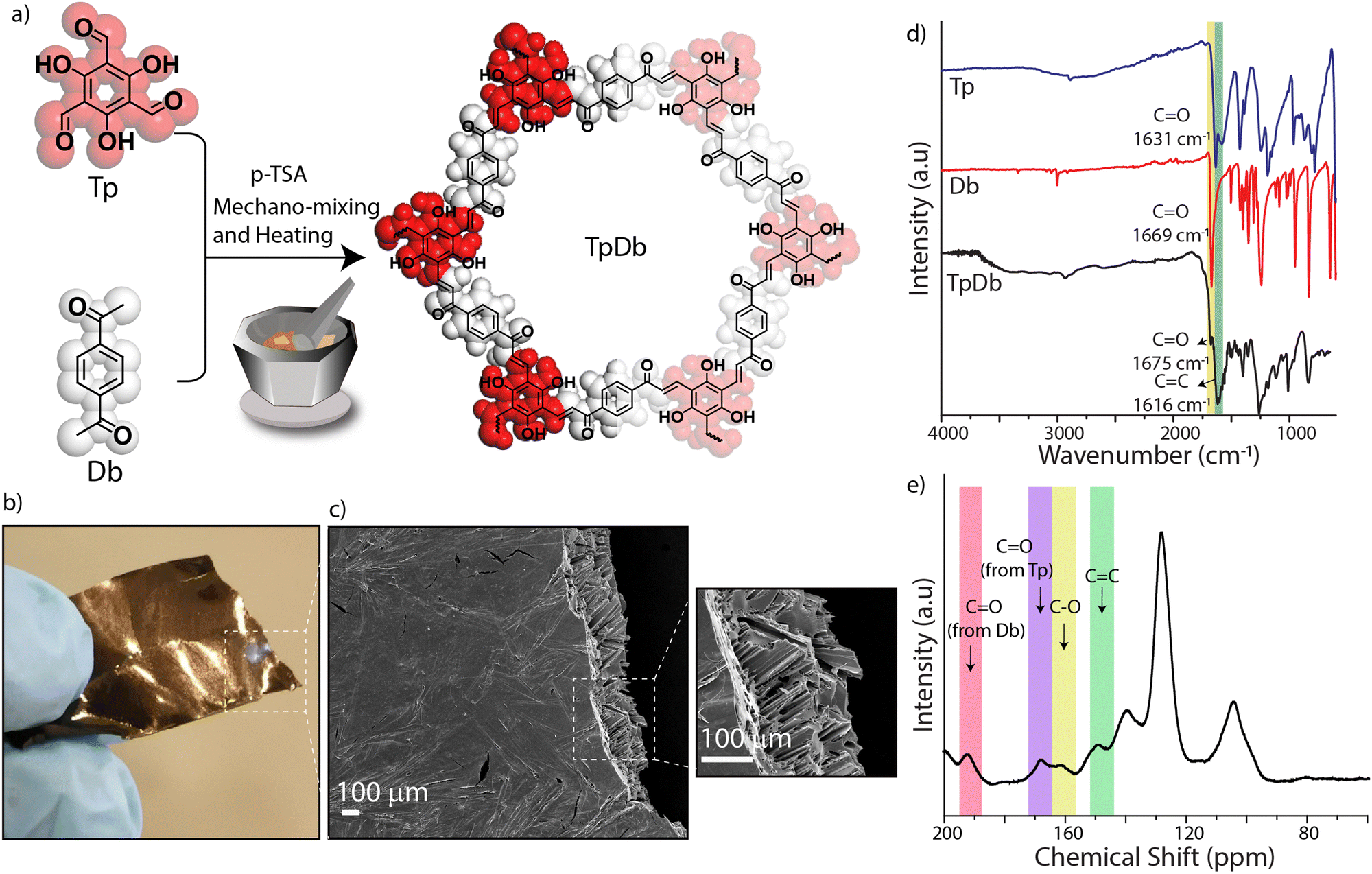 | ||
| Fig. 1 (a) The scheme of TbDb synthesis. (b) A digital photograph of the TpDb free-standing sheet. (c) The SEM image of TpDb. (d) The FT-IR of TpDb with monomers. (e) The 13C solid-state NMR of TpDb. | ||
The Fourier-transform infrared (FT-IR) spectroscopy revealed the chemical bonding features of TpDb (Fig. 1d). Notably, the absence of a characteristic aldehyde CO peak at 1636 cm−1 from Tp indicates the aldol condensation reaction at Tp aldehydes. Moreover, the stretching vibration at 1610 cm−1 corresponds to the newly formed CC bonds and the presence of a ketone CO peak at 1683 cm−1 suggests the formation of a conjugated enone in the framework upon the dehydration process. The formation of the allyl ketone (CC–CO) structure signifies successful Aldol condensation. Furthermore, the presence of weak doublet peaks at 2875–2925 cm−1 could be originated from the residual aldehyde C–H stretching, indicating the possibility of defects in the 2D framework. The 13C solid-state NMR spectroscopy further validated the enone structure of the TpDb (Fig. 1e). The presence of the CO from the enone was confirmed at ∼192 ppm. Additionally, the characteristic olefin CC signal and the C–O signal were noted at 149 ppm and 161 ppm, respectively. The above observations indicate the formation of olefin-connected polymeric networks. Interestingly, the peak at 167 ppm could originate from the CO from Tp in the framework due to the possible tautomerism between the newly formed conjugated enone and enol in Tp.
Notably, TpDb is a 2D-polymer, constructed using conjugated sp2 carbon atoms from symmetric planar building blocks (C3 and C2). The physical appearance of the as synthesized TpDb resembles hard-rocks, which could be due to the efficient packing of 2D layers through intermolecular weak interactions like hydrogen bonding and π–π stacking. The powder X-ray diffraction (PXRD) of TpDb is investigated to understand the periodic nature of the polymer (Fig. 2a). The PXRD profile of TpDb shows a broad peak at 2θ ∼ 8.0° along with a broad amorphous peak range of 2θ ∼ 15° to 30°. Although it is difficult to build an exact structure of TpDb using the obtained PXRD, theoretical models were constructed to understand the possible mode of layer stacking in TpDb (Fig. S3, ESI†). Interestingly, the ABC stacking of 2D layers is best matched with the experimental PXRD compared to AA, slip-AA, and AB stacking of layers (Fig. 2b). We surmise that the ABC stacking of TpDb could be due to the possible interlayer hydrogen bonding between CO and C–O–H (3.1 Å) (Fig. 2c). Compared to other stacking modes, the ABC stacking results in maximum close packing of the layers, which creates ultramicroporous channels. Furthermore, it forms high-density occupancy of functional groups in the polymeric matrix of TpDb. Interestingly, the broad peak observed in TpDb suggests its semicrystalline nature, characterized by numerous structural defects, in contrast to highly crystalline COFs. This lower crystallinity, coupled with the presence of structural defects, may offer potential advantages in enhancing charge-trapping properties.
 | ||
| Fig. 2 (a) The experimental PXRD profile of TpDb with simulated PXRD of the ABC stacking model. (b) The theoretical models of the ABC stacking model of TpDb (2 × 2 cells). (c) The vertical view of the ABC-stacked model of TpDb along with the possible interlayer interaction through hydrogen bonding. (d) and (e) Total charge density distribution across different atoms (isosurface = 0.3) in TpDb. (f) Cross-sectional schematic diagram of the MOS capacitor device. (g) FIB assisted HRSEM cross-sectional image of the MOS capacitor (Al/Al2O3/TpDb/Al2O3/Si) device. (h) SEM image of TpDb flakes using the drop-casting technique at 100 μm scale, showing highly dense flakes all over the surface. | ||
The solid-state UV-visible spectroscopy of TpDb showed a broad visible range absorption from 600 nm to 400 nm with wavelength maxima at 474 nm and 590 nm (Fig. S4, ESI†). The Tauc plot suggests an optical band gap value of 2.7 eV (Fig. S5, ESI†). The electrical conductivity measurements of free-standing sheets of TpDb were analyzed by a four-probe method using the Signatone probe station, which showed a conductivity of 6.075 × 10⁻⁹ ± 0.245 × 10⁻⁹ S m−1 (Fig. S6–S8, ESI†). The low conductivity is attributed to the semiconjugation of the TpDb network and structural defects. The thermogravimetric analysis showed that the thermal stability of TpDb was maintained up to 200 °C (Fig. S9, ESI†).
The DFTB calculation, conducted on the ABC stacked model of TpDb, provides insights into the charge density distribution across the network (Fig. 2d and e). The results distinctly reveal that oxygen atoms exhibit electron-rich characteristics, whereas hydrogen atoms, particularly the phenolic proton, appear electron-deficient. The electronic distribution within the framework suggests a potential for interlayer hydrogen bonding in TpDb. We hypothesize that, along with structural defects, these hydrogen-bonding sites may serve as potential charge-trapping levels in TpDb, given the functional interactions (CO with C–O–H) within the polymeric layers. Moreover, electron affinity (Eea), a pivotal parameter influencing charge trapping efficiency, is determined by assessing the energy difference between the vacuum level (Evac) and the conduction band minimum (EC).10 The calculated Eea of 3.14 eV (with respect to the vacuum level), underscores the material's robust inclination to attract electrons. This observation aligns with the behavior seen in conjugated polymers, where Eea typically spans from 1 to 4 eV (with respect to the vacuum level).11
To understand the charge-trapping behavior, TpDb was employed as a charge-trapping layer in a non-volatile MOS capacitive device. The MOS capacitor memory device is fabricated on a p+Si substrate, as shown in Fig. S10 and 11 (ESI†). In the first step, a p+Si wafer was etched using buffer oxide etchant (BOE) for 3 min to remove the native oxide and washed with deionized water. Then, the wafer was cleaned using a nitrogen gun to remove the native oxide. Next, an Al2O3 tunneling layer of 3 nm thickness was deposited by plasma-enhanced atomic layer deposition (PE-ALD) at 250 °C using Al (CH3), trimethylaluminum, and O2 plasmas as the Al and O precursors. Furthermore, a charge-trapping layer TpDb was drop cast on the tunneling layer using the TpDb solution and then the device was dried initially at 80 °C temperature using a hot plate and later at room temperature for 5 hours. Thereafter, a 15 nm thick Al2O3 blocking oxide layer was deposited on TpDb by PE-ALD. Finally, an Al layer top electrode of 120 nm was deposited via direct current magnetron sputtering using a metal shadow mask. Fig. 2f and g are the cross-sectional schematic diagrams of the MOS capacitor device architecture and FIB (focused ion beam) assisted HRSEM (high resolution scanning electron microscopy) cross-sectional images, respectively. Fig. 2f–h clearly shows the TpDb film with a thickness of ∼60 nm sandwiched between the Al2O3 (tunneling layer ∼ 3 nm) and the Al2O3 (blocking oxide layer ∼ 15 nm). The SEM image for the drop-cast TpDb reveals the morphology, compactness, and high density of the drop-cast layer (Fig. 2h). The results verify the high density of TpDb flakes with different dimensions. It is anticipated that the 2D flakes with a highly dense arrangement are responsible for a larger charge trapping density at the Al2O3/TpDb interface or within the TpDb layer in the device, thus enabling a larger memory window.
Fig. 3a displays the multi-cycling (1st, 100th, 500th, 800th, 1000th cycles) capacitance–voltage (CV) characteristics when programming by sweeping the gate voltage from +3 V to −2 V and while erasing by sweeping the gate voltage from 3 V to −2 V, at a 100 kHz frequency at room temperature. A stable and wide memory window of ∼3.2 V is observed at such low program/erase voltages. It is also evident that after 1000 cycles, a negligible shift in the CV curve is observed compared to the 1st cycle. The breakdown electric field intensity (E) range between 1.94 and 1.75 MV cm−1 across the TpDb layer (see Fig. S12) was calculated (details are in ESI†). To confirm the interface trapping, the C–V curve at different frequencies was also analyzed (inset of Fig. 3a). Additional frequency-dependent C–V characteristics are also shown in the ESI† (see Fig. S13). The frequency hysteresis (Fig. S13, ESI†) confirms the presence of an interfacial state at the Al2O3/TpDb interface. Fig. 3b shows the threshold voltage at different programming/erasing (P/E) voltages from ±2 V up to ±8 V. A noticeable increase in the memory window is observed, which confirms that a large charge trapping density is available within the TpDb. This could be due to high-density packing of the TpDb network, which provides more trapping sites per unit volume. More specifically, at ±8 V sweeping voltages, a remarkable 8 V memory shift is obtained. The observed shift of the threshold voltage towards both negative and positive directions during the different sweeping conditions indicates that both hole and electron trapping are achieved in the TpDb layer.12,13 These observations signify the presence of charge-trapping sites within TpDb that can stabilize both positive and negative charges through weak molecular interactions such as hydrogen bonding. The current–voltage characteristics across the device are also measured (Fig. S14, ESI†), which shows the low gate leakage current.
 | ||
| Fig. 3 (a) Capacitance–voltage (C–V) characteristics of the MOS capacitor at a ±3 V bi-directional sweeping voltage showing the charge trapping phenomenon over 1000 cycles at room temperature (RT). (b) Threshold voltage (Vt) under different bi-direction scan voltage ranges at 100 kHz frequency. (c) Extracted charge trapping density (CTD) as a function of P/E voltage. (d) Device-to-device stability of 10 random devices. (e) Endurance of the MOS capacitor. (f) Retention characteristics of the MOS capacitor at room temperature (RT) and at 100 °C. | ||
Furthermore, the charge trapping density in the storage layer at different program/erase voltages (Fig. 3c) is calculated using the equation Nt = Ct × △Vt/q, where Ct is the capacitance of the device per unit area, △Vt is the memory window of the device at VFB and q is the elementary charge. It is clear that the trapped charge density increases at larger operating voltages, reaching a high value of 1.562 × 1013 cm−2 at 8/−8 V P/E voltages. The device-to-device stability of ten randomly chosen devices is estimated and the corresponding memory window for all ten devices is found to be ∼3.2 V (Fig. 3d). This result confirms the excellent stability of all devices for both programming and erasing states, even though the drop-casting technique does not usually result in a good uniformity of the deposited layer; thus, a different density of flakes is expected to exist within the different devices. However, the stable results and low device-to-device variability confirm that the large charge trapping density within the TpDb is larger than the number of charges tunneling at a specific P/E voltage. To test the endurance of the MOS memory, the device was P/E using voltages of +3/−2 and −3/+2 (Fig. 3e). The device shows good endurance up to 104 cycles without any degradation. Fig. 3f demonstrates the retention performance measured at both room temperature (RT) and at 100 °C using the P/E voltages of +3/−2 and −3/+2, respectively. A good memory window was observed at RT for 104 seconds. While by increasing the temperature up to 100 °C, the memory window is reduced by a negligible voltage, which confirms that it can also withstand up to 104 seconds. Therefore, the MOS memory shows good retention properties (up to 104 seconds) with a wide memory window (∼3.2 V), even when stressed at an elevated temperature of 100 °C. These noticeable retention characteristics could be due to the large conduction and valence band shifts between the TpDb and surrounding oxides, resulting in a large charge potential barrier during the retention operation. Such excellent endurance and retention properties along with the large memory hysteresis make the TpDb promising for non-volatile memory applications compared with other reported materials (Fig. 4a and b).14–22 Overall, the TpDb-based device was reliable up to 104 cycles and it showed over 52% increase in memory window compared to previously demonstrated devices while using a lower P/E voltage. It should be noted that the memory hysteresis reported in ref. 15, 16, and 19 is not reported on the graph as the used P/E voltages were very large (>50/−50 V). Thus, TpDb-based MOS memory stands out as a highly promising device for non-volatile memory applications.
 | ||
| Fig. 4 (a) and (b) represent the comparison of the endurance and memory window of our MOS capacitor device with previously reported work. (c) The energy band diagram of the MOS capacitor (Al/Al2O3/TpDb/Al2O3/Si) structure (flatband condition). (d) and (e) The program and erase operations of the CTM, respectively. | ||
To better explain the physics of the device, the charge-trapping memory's energy band diagram (Fig. 4c) is constructed incorporating the Eea value of TpDb calculated using DFT calculations and the reported band offsets and bandgaps of the used materials.23 When program voltage sweeps (+3 V to +2 V) are applied to the MOS gate (Fig. 4d), electrons in Si conduction states gain sufficient energy to tunnel through the Al2O3 and become trapped within the TpDb's quantum well formed by the band offsets and within the interface states along the alumina. Simultaneously, holes in the TpDb acquire enough energy to be emitted into the p+Si substrate. Similarly, Fig. 4e shows the erase operation of the memory.
These results show (Fig. 3a) a right shift of the memory's programmed C–V characteristic (Vt–1 V). Conversely, during the erase voltage sweeps (−3 V to 2 V), electrons from the TpDb tunnel back to the Si bulk, while holes are ejected into the TpDb. This causes the C–V characteristic of the memory to shift back to the left (Vt ∼ −2 V). The large band offsets between the TpDb and surrounding oxides explain the excellent retention characteristic of the memory.
Conclusions
In conclusion, we have developed a novel carbonyl-decorated semi-conjugated 2D-polymer through solid-state mechanomixing synthesis. The resulting 2D-polymer showed a high-density packing of the network layers with the potential capability of trapping charges through weak interactions and structural defects. The TpDb-based capacitive memory device (Al/Al2O3/TpDb/Al2O3/Si) showed a wide memory window (∼3.2 V) at low programming and erasing voltages of +3/–2 V and –3/+2 V. An excellent stability and small variation was obtained for ten random devices. Furthermore, the devices also display desirable reliability characteristics in terms of a robust endurance performance (10000 cycles) and a good 104 seconds retention at an elevated temperature of 100 °C. Moreover, these excellent features demonstrated charge trapping in the TpDb-based MOS memory, unlocking the potential for future non-volatile memory applications.
Author contributions
RAA: data curation; formal analysis; investigation; methodology. AKM: conceptualization; data curation; formal analysis; investigation; methodology; validation; visualization; roles/writing – original draft. PP: data curation; formal analysis; investigation; methodology; validation; visualization; roles/writing – original draft. MAA: data curation; investigation; methodology; software. SSN: data curation; investigation; methodology; roles/writing – original draft, software. DK: investigation; methodology. AMS: investigation; methodology. AR: investigation; methodology. NS: data curation; investigation; methodology; resources; software; supervision; validation; writing – review & editing. AN: data curation; investigation; methodology; resources; supervision; validation; writing – review & editing. NEA: data curation; investigation; methodology; resources; supervision; validation; writing – review & editing. DS: conceptualization; funding acquisition; project administration; resources; supervision; validation; writing – review & editing.Conflicts of interest
There are no conflicts to declare.Acknowledgements
RAA, AKM, and DS acknowledge Khalifa University Abu Dhabi for the generous support of this research. DS acknowledges the financial support from the Khalifa University Competitive Internal Research Award (CIRA-2021). DS acknowledges resource support under the Center for Catalysis and Separations (CeCaS). AN and AZ acknowledge the financial support from Aspire as part of the VRI20-07. The authors (PP, DK, AMS, and NEA) would like to acknowledge generous financial support from King Abdullah University of Science and Technology (KAUST) Research Funding (KRF) under Award No. OFP-2023-5518. MAA is grateful for HPC resources via membership of the UK's HEC Materials Chemistry Consortium, which is funded by EPSRC (EP/X035859), this work used the UK Materials and Molecular Modelling Hub, which is partially funded by EPSRC (EP/T022213).Notes and references
- D. Abbaszadeh, A. Kunz, N. B. Kotadiya, A. Mondal, D. Andrienko, J. J. Michels, G.-J. A. H. Wetzelaer and P. W. M. Blom, Chem. Mater., 2019, 31, 6380–6386 CrossRef CAS.
- H. F. Haneef, A. M. Zeidell and O. D. Jurchescu, J. Mater. Chem. C, 2020, 8, 759–787 RSC.
- Y. van de Burgt, A. Melianas, S. T. Keene, G. Malliaras and A. Salleo, Nat. Electron., 2018, 1, 386–397 CrossRef.
- F. Alibart, S. Pleutin, O. Bichler, C. Gamrat, T. SerranoGotarredona, B. Linares-Barranco and D. Vuillaume, Adv. Funct. Mater., 2012, 22, 609–616 CrossRef CAS.
- A. M. Evans, M. J. Strauss, A. R. Corcos, Z. Hirani, W. Ji, L. S. Hamachi, X. A.-Enriquez, A. D. Chavez, B. J. Smith and W. R. Dichtel, Chem. Rev., 2022, 122(1), 442–564 CrossRef CAS PubMed.
- B. Sun, X. Li, T. Feng, S. Cai, T. Chen, C. Zhu, J. Zhang, D. Wang and Y. Liu, ACS Appl. Mater. Interfaces, 2020, 12, 51837–51845 CrossRef CAS PubMed.
- A. Rezk, Md. H. R. Ansari, K. C. Ranjeesh, S. Gaber, D. Kumar, A. Merhi, B. R. Kaafarani, M. B. Hassine, N. E. Atab, D. Shetty and A. Nayfeh, Sci. Rep., 2023, 13, 18845 CrossRef CAS PubMed.
- P.-K. Zhou, H. Yu, Y. Li, H. Yu, Q. Chen and X. Chen, J. Polym. Sci., 2023, 1–18, DOI:10.1002/pol.20230273.
- J. Kang, S. Huang, K. Jiang, C. Lu, Z. Chen, J. Zhu, C. Yang, A. Ciesielski, F. Qiu and X. Zhuang, Adv. Funct. Mater., 2020, 30, 2000857, DOI:10.1002/adfm.202000857.
- Z. Zhang, M. Wensell and J. Bernholc, Phys. Rev. B: Condens. Matter Mater. Phys., 1995, 51, 5291–5296 CrossRef CAS PubMed.
- D. Abbaszadeh, A. Kunz, N. B. Kotadiya, A. Mondal, D. Andrienko, J. J. Michels, G.-J. A. H. Wetzelaer and P. W. M. Blom, Chem. Mater., 2019, 31, 6380–6386 CrossRef CAS.
- E. Zhang, W. Wang, C. Zhang, Y. Jin, G. Zhu, Q. Sun, D. W. Zhang, P. Zhou and F. Xiu, ACS Nano, 2015, 9, 612–619 CrossRef CAS PubMed.
- W. Guan, S. Long, M. Liu, Z. Li, Y. Hu and Q. Liu, J. Phys. D: Appl. Phys., 2007, 40, 2754–2758 CrossRef CAS.
- D. Prime, S. Paul and P. W. Josephs-Franks, Philos. Trans. R. Soc., A, 2009, vol. 367, 1905, DOI:10.1098/rsta.2009.0141.
- J.-H. Hong, S. H. Kim, S. B. Jo, K. Cho and B. Kang, Org. Electron., 2011, 93, 106107 CrossRef.
- N. M. Murari, Y.-J. Hwang, F. S. Kim and S. A. Jenekhe, Org. Electron., 2016, 31, 104–110 CrossRef CAS.
- J.-S. Lee, J. Cho, C. Lee, I. Kim, J. Park, Y.-M. Kim, H. Shin, J. Lee and F. Caruso, Nat. Nanotechnol., 2007, 2, 790–795 CrossRef CAS PubMed.
- W. L. Leong, P. S. Lee, A. Lohani, Y. M. Lam, T. Chen, S. Zhang, A. Dodabalapur and S. G. Mhaisalkar, Adv. Mater., 2008, 20, 2325–2331 CrossRef CAS.
- S.-T. Han, Y. Zhou, Z.-X. Xu, L.-B. Huang, X.-B. Yang and V. A. L. Roy, Adv. Mater., 2012, 24, 3556–3561 CrossRef CAS PubMed.
- E. H. Oulachgar, C. Aktik and M. Scarlete, IEEE Trans. Electron Devices, 2010, 57, 1942–1947 CAS.
- V. Suresh, M. S. Huang, M. P. Srinivasan and S. Krishnamoorthy, J. Mater. Chem., 2012, 22, 21871–21877 RSC.
- A. Miura, Y. Uraoka, T. Fuyuki, S. Kumagai, S. Yoshii, N. Matsukawa and I. Yamashita, Surf. Sci., 2007, 601(15), L81–L85 CrossRef CAS.
- E. Bersch, S. Rangan, R. A. Bartynski, E. Garfunkel and E. Vescovo, Phys. Rev. B: Condens. Matter Mater. Phys., 2008, 78, 085114 CrossRef.
Footnotes |
| † Electronic supplementary information (ESI) available: Experimental section. See DOI: https://doi.org/10.1039/d4mh00201f |
| ‡ RAA, AKM, and PP made equal contributions to this manuscript. |
| This journal is © The Royal Society of Chemistry 2024 |