
 Open Access Article
 This Open Access Article is licensed under a
 Creative Commons Attribution 3.0 Unported Licence
Bicolour, large area, inkjet-printed metal halide perovskite light emitting diodes†
Vincent R. F.
Schröder
 a,
Nicolas
Fratzscher
b,
Nicolas
Zorn Morales
b,
Daniel Steffen
Rühl
b,
Felix
Hermerschmidt
*b,
Eva L.
Unger
cde and
Emil J. W.
List-Kratochvil
*ab
a,
Nicolas
Fratzscher
b,
Nicolas
Zorn Morales
b,
Daniel Steffen
Rühl
b,
Felix
Hermerschmidt
*b,
Eva L.
Unger
cde and
Emil J. W.
List-Kratochvil
*ab
aHelmholtz-Zentrum Berlin für Materialien und Energie, Hahn-Meitner-Platz 1, 14109 Berlin, Germany
bInstitut für Physik, Institut für Chemie, IRIS Adlershof, Humboldt-Universität zu Berlin, Zum Großen Windkanal 2, 12489 Berlin, Germany. E-mail: felix.hermerschmidt@hu-berlin.de; emil.list-kratochvil@hu-berlin.de
cDepartment Solution Processing of Hybrid Materials & Devices, Helmholtz-Zentrum Berlin für Materialien und Energie, Kekuléstraße 5, 12489 Berlin, Germany
dInstitut für Chemie, IRIS Adlershof, Humboldt-Universität zu Berlin, Zum Großen Windkanal 2, 12489 Berlin, Germany
eChemical Physics and NanoLund, Lund University, PO Box 124, 22100 Lund, Sweden
First published on 8th February 2024
Abstract
We demonstrate a bicoloured metal halide perovskite (MHP) light emitting diode (LED) fabricated in two sequential inkjet printing steps. By adjusting the printing parameters, we selectively and deliberately redissolve and recrystallize the first printed emissive layer to add a pattern emitting in a different color. The red light emitting features (on a green light emitting background) have a minimum size of 100 μm and originate from iodide-rich domains in a phase-segregated, mixed MHP. This phase forms between the first layer, a bromide-based MHP, which is partially dissolved by printing, and the second layer, an iodide-containing MHP. With an optimised printing process we can retain the active layer integrity and fabricate bicolour, large area MHP-based LEDs with up to 1600 mm2 active area. The two emission peaks at 535 nm and 710 nm are well separated and produce a strong visual contrast.
New conceptsLight emitting diodes (LEDs) based on metal-halide perovskites (MHP) have already been demonstrated for the emission of red, green and blue light. To achieve simultaneous emission of multiple colours, previous approaches focused on the fabrication of tandem devices with multiple emitter layers or on the creation of multiple emission colours by adding emissive additives into the MHP precursor solution. These approaches, however, do not allow selective patterning of the emissive layer. Here, we demonstrate a two-step inkjet printing process to directly pattern a homogeneous MHP film. By controlling the substrate temperature, ink formulation and drying procedure, we can selectively and deliberately redissolve and recrystallize the primary emissive layer and achieve homogeneous, smooth and pinhole-free patterned emissive layers. With optimised printing conditions we ensured the full integrity of the patterned layer and attained a minimum feature size of 100 μm for a single printed dot. The fabricated devices show no increase in leakage current or decrease of device performance caused by the patterning procedure. Here this two-step printing process was successfully used to realise large area, bicoloured perovskite LEDs, yet it can be generally applied in any device structure where a spatially controlled variation of the material composition is needed. |
Introduction
MHPs are a solution-processable, crystalline class of semiconductors, that are employed in a multitude of high efficiency optoelectronic devices, such as solar cells,1–3 photodetectors,4–6 X-ray detectors7–9 and light emitting diodes.10–13 The solubility of the MHP precursors in polar solvents enables solution processing by spin-coating, slot-die coating14,15 and inkjet printing (IJP).16–20 IJP printing offers large-area, structured and selective deposition of materials with high throughput and inline process integration. We have demonstrated in earlier studies that bright perovskite-based LEDs (PeLEDs) could be frabricated by inkjet printing and upscaled to 1600 mm2 active area size.21,22Beyond large area processing, IJP enables the generation of arbitrary patterns from digital sources through selective drop placement.23,24 Precise control over deposited droplets enables combinatorial mixing of inks during the deposition process, which also enables high-throughput compositional screening of perovskite materials.25,26
A key feature that makes MHPs an interesting material for different applications is the tunable, composition-dependent bandgap. Let us consider methyl ammonium lead bromide (MAPbBr3) with a bandgap of 2.3 eV. The bandgap of e.g. methyl ammonium (MA) containing MHPs can be tuned by substituting the halide anion component, which allows seamless tuning of the MHP bandgap towards lower energies by partial substition of Br− by I− (MAPbIxBr1−x) or higher energies by substituting Br− with Cl− (MAPbClxBr1−x).27 By tuning the halide composition, the perovskite lattice is expanded or compressed and bandgap energies between 1.6 eV (MAPbI3) and 3.1 eV (MAPbCl3) can be achieved. Alternatively, the bandgap of MAPbBr3 can be expanded by substituting MA with large A-site cations, such as phenethyl ammonium (PEA) cations, which creates a layered, 2D structure, with an increased bandgap of 3.1 eV for e.g. PEA2PbBr4.28 Mixing of these cations enables fine tuning of the bandgap, by controlling the number of lead-octahedral layers between the large PEA spacer ions.29–31 As a result, semiconductor devices which absorb or emit specific wavelengths of light in the visible spectrum can be fabricated.32–34
Tuning the bandgap by means of halide compositional engineering is powerful, but in reality subject to compositional phase segregation.35–37 For mixed halide perovskites, the disproportionation of the mixed-halide solid solution into a wide phase distribution is well known.38–41 This effect has already proved harmful in MHP solar cells, but is catastrophic for light emitting devices, as injected charge carriers are funneled into low bandgap domains of the mixed-halide phase distribution.42–44 A strong red-shift of the emitted light is the result.45,46 Subsequently, colour stabilty in PeLEDs became a topic of substantial interest in recent years and good progress was made, mainly by surpressing ion migration with large spacer ions.47,48 Single colour PeLEDs can be combined in a matrix towards display applications,49,50 and beyond single-colour emission of a single device, multiple approaches were tested in literature. To yield multiple emission wavelengths from a single device, two separate electroluminescent MHP layers,51 a partial colour conversion layer,52,53 or the introduction of a secondary emitter material in the electroluminescent perovskite layer by phase separation or blending with an organic molecule have been previously used.54,55 These works all focused on the fabrication of white light emitting devices by colour mixing. Creating a structured emission pattern in a PeLED remains challenging, due to the difficulty in controlling the drying behaviour of MHP inks, which tend to hamper the structural integrity of the printed thin films.23 While structuring of an MHP layer for multi-coloured photoluminescent MHP layers has been shown by lithography,56 inkjet printing,57 and E-jet printing,58 a structured, multi-coloured electroluminescent emission pattern from a single LED pixel could not yet be demonstrated.
In this study, we demonstrate direct patterning of the electroluminescent layer using IJP. By inducing spatially selective phase segregation, we confined the red-shift of mixed halide perovskite phases to a printed pattern and achieved bicolour emission from a single emission layer. For this, an area up to 1600 mm2 Br− based MHP layer was first deposited by inkjet printing. To achieve a high quality MHP layer of that size, a special gas flow assisted drying method was used.16 A custom-made aluminium chamber was evacuated and a constant nitrogen stream, shaped by a 3D printed slit-nozzle, dried the printed, wet film which crystallized into a homogeneous and pinhole-free large area MHP layer. In a second printing step, an I−-based MHP composition was printed on top of the first layer, partially redissolving the dried perovskite in the process and forming a mixed-composition perovskite phase. By exploiting the segregation of the mixed-halide perovskite phase, we achieved arbitrarily patternable bicolour PeLEDs with a single emitter layer and strong colour contrast.
Results
To achieve a single emitter layer with a lateral emission pattern, we used a sequential IJP process. In a first step, the active device is printed from a MAPbBr3:poly(ethylene glycol) (PEG) ink using dimethyl formamide (DMF), dimethylsulfoxide (DMSO) and gamma-butyrolactone (GBL). The dried MHP layer acts as green light emitter in the fabricated PeLEDs. The ink is deposited on a substrate with a prepatterned indium tin oxide (ITO) electrode coated with a poly(3,4-ethylenedioxythiophene):polystyrene sulfonate/potassium chloride (PEDOT:PSS/KCl) layer. The resulting wet film is dried in a gas flow assisted vacuum chamber. Further details of this process are described in our previous publications.21,22Printing a patterned MHP layer
To directly print the patterned emissive structure in a second step, we used a PEA2MA3Pb4I13 composition, which acts as red light emitting material (Fig. 1a). In this second printing step, the underlying layer is partially dissolved. The dissolved area thus contains a mixture of the ionic components of the first layer and the MHP precursors in the second ink. This second ink contains the MHP precursors in a solvent mixture of GBL and chlorobenzene (CBZ) in a 3![[thin space (1/6-em)]](https://www.rsc.org/images/entities/char_2009.gif) :1 ratio. When designing the ink formulation, we considered the loading of the ink with MHP precursors and the solubility of the first layer. With a high precursor loading, the added material would increase the layer thickness of a patterned area and reduce current density and therefore light emission in this part of the device. Additionally, since the second printing step dissolves the first layer, using more polar solvent dissolves more MHP and thereby increases the minimum feature size. The GBL/CBZ mixture was therefore chosen to create a saturated ink with low precursor concentration, dissolving as little as possible of the first underlying layer and at the same time adding little material to the printed layer.
:1 ratio. When designing the ink formulation, we considered the loading of the ink with MHP precursors and the solubility of the first layer. With a high precursor loading, the added material would increase the layer thickness of a patterned area and reduce current density and therefore light emission in this part of the device. Additionally, since the second printing step dissolves the first layer, using more polar solvent dissolves more MHP and thereby increases the minimum feature size. The GBL/CBZ mixture was therefore chosen to create a saturated ink with low precursor concentration, dissolving as little as possible of the first underlying layer and at the same time adding little material to the printed layer.
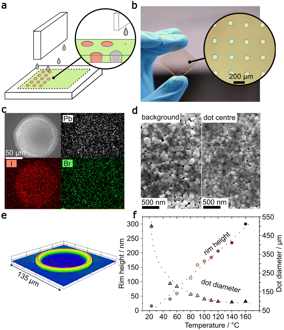 | ||
| Fig. 1 (a) The sequential printing process with a large area of MAPbBr3 as background layer in which PEA2MA3Pb4I13 is printed on top with (b) a feature size that cannot be perceived by eye. (c) The printed dots have a diameter of 125 μm and EDX confirms the existence of iodide exclusively in the printed dots. (d) SEM shows the morphology of the background layer and printed dots. (e) A 3D confocal microscope image shows a large dot rim height, which (f) can be adjusted by substrate temperature. | ||
Initiated by the undissolved edge of the crystalline first layer, the MHP precursors in the dissolved area recrystallize and form a mixed cation, mixed halide lead perovskite. Fig. 1b shows a photograph of a patterned perovskite layer. Macroscopically, the first layer retains the faint yellow colour of the pure MAPbBr3:PEG layer. Printed features are not distinguishable from the background at normal lighting conditions by the naked eye. As inset, a microscope image of the patterned layer is shown.
The printed dots have a diameter of 100 μm and a distance of 300 μm. In Fig. 1c, a scanning electron microscope image of a printed feature shows the dimensions of a dot with a diameter of 125 μm. Using energy dispersive X-ray spectroscopy (EDX), I− ions are shown to be exclusively present in the printed dot, while Pb2+ and Br− ions are universally present. Fig. 1d shows the morphology of the first perovskite layer and the centre of the printed dots. The perovskite crystal of the underlying background layer features a crystal size around 200 nm, which decreases after dissolving and recrystallization, resulting in smaller, around 100 nm large crystals. The dissolving-recrystallizing process creates well defined dots of mixed-halide perovskite and confines the I−-based perovskite added in the second printing step. In this process, the lateral dimension of the printed dots depends solely on the dissolving of the underlying layer, while the feature height and thereby the roughness of the resulting patterned layer depends on the recrystallization.
To tune the dimensions of the printed features, we controlled the substrate temperature during the second printing step with an external hotplate fixed on the printing table. Fig. 1e displays a 3D image of a single dot taken with a confocal laser microscope. The dot was printed with a substrate temperature of 120 °C and shows a strong coffee ring effect. The interplay of rim height and dot diameter of the printed features for substrate temperatures between glovebox temperature (RT = 25 °C) and 160 °C is shown in Fig. 1f. At room temperature, the printed features have a width up to 500 μm with a ca. 20 nm high rim at the edge of the dot. With increasing temperature, the width of the feature decreases to less than 100 μm but the roughness of the resulting patterned layer is affected drastically. Rim heights up to 300 nm were measured.
Increasing the temperature accelerated the evaporation of the solvents in the ink, which limits the spreading of ink on the solid layer and facilitates fast crystallization, templated by the crystalline, undissolved edge of the remaining solid layer. At sufficiently high temperature (relative to the boiling point and vapour pressure of the solvent system) the droplets are pinned to the surface, reaching minimal lateral feature size. Considering the thickness of the initial solid layer of 60 nm, the resulting rim height proved challenging for integration in a multi-layer PeLED structure, causing shorts, reducing device performance and ultimately leading to device failure. Fig. 1f shows that shrinking the dot diameter by increasing the substrate temperature results in an increasing rim height. To ensure optimum device functionality, perovskite layers for PeLED devices were printed at room temperature with a targeted dot diameter of 100 μm. In order to reach this, the drop volume of the second printing step was reduced from 30 pL to 1 pL by changing the print head system. This smaller drop volume was used to create printed features in MHP layers for further characterization and PeLED fabrication.
Exploiting MHP phase segregation
The dissolving and recrystallising process of the second printing step creates an MHP composition containing components of the MAPbBr3:PEG background layer and the PEA2MA3Pb4I13 ink. The bandgap of this mixed composition depends primarily on the halide ratio. To investigate the ionic composition of the patterned MHP layer, a sample series with decreasing dot distance was printed. Fig. 2a shows microscopy images of the unpatterned first layer and four decreasing dot distances (250 μm, 200 μm, 150 μm and 100 μm). Due to the dot diameter of 100 μm, the dots can only be clearly distinguished until a centre-to-centre distance of 100 μm, at which the printed dots start to overlap. Thus, for the closest spacing, the result is a rough layer with an interference-like pattern. In this series, the total volume of deposited I−-based ink, and therefore the I−/Br− ratio is increasing. | ||
| Fig. 2 (a) A series of patterned perovskite layers with decreasing dot distance from 250 μm to 100 μm and corresponding average iodide/bromide ratio up to 2.4% were fabricated, which show a shift of the (b) UV-vis spectrum and (c) XRD pattern. (d) μm-scale PL measurements of the patterned layer show the emission of the background, printed dot and dot edge. | ||
Using the concentration of Br− and I−-based inks, we calculated the nominal I−/Br− ratio from the deposited ink volume and stoichiometry of the perovskite compositions (see ESI†). For a decreasing drop distance from 250 μm to 100 μm, the nominal I−/Br− ratio increases from 0.4% to only 2.4%. This low iodide content in a fully dissolved and recrystalized layer is mainly due to the lower drop volume (1 pL compared to 24 pL) and lower print resolution. Fig. 2b shows the absorption edge of the patterned layers from UV-vis measurements. For higher dot distances, the observed shift lies between 3 nm and 5 nm and only for the lowest centre-to-centre dot distance of 100 μm (i.e. 2.4% ratio) a significant shift of 15 nm was observed. The widening of the bandgap (∼60 meV) linearly correlates to the halide ratio in the solid film. Using the known absorption spectra of pure MAPbBr3 and MAPbI3,26 the red shift of 15 nm corresponds to an MHP composition containing ∼6.3% I−. The discrepancy from the nominal ratio is most likely due to variations in the printed drop volume (Fig. S4, ESI†). For the primary printhead system, a drop volume between 20 pL and 28 pL were determined. The smaller, nominally 1 pL droplets of the secondary printhead system could not be verified by the PixDRO printed dropwatcher analyser software.
Besides the change of the bandgap, the incorporation of iodide causes expansion of the unit cell latice, which can be determined by XRD. Fig. 2c shows the first reflection peak of the cubic perovskite phase for the sample series. While larger dot distances again barely show an effect, the 100 μm dot distance sample displays a shift in the reflection by ∼0.08°, which corresponds to the incorporation of ∼8.8% I−. These estimations are also based on linear interpolation of the XRD reflections of pure MAPbBr3 and MAPbI3.26 This value is close to the 6.3% extracted from UV-vis and deviates due to the inhomogeneous nature of the sample and thus a decreased detection limit.59 The ratio of PEA cations to I− in the second ink is 2:13 and thus below 1% in the patterned perovskite layer. As such, the possible impact of 2D phases on the absorption edge and XRD pattern is negligible.
If we further assume that the shortest dot spacing of 100 μm in Fig. 2a corresponds to a fully dissolved and recrystallized perovskite film, we can safely estimate that the I−/Br− ratio in our printed pattern does not exceed 10%. This would ideally correspond to a red shift of the emission wavelength of ∼25 nm to 560 nm. Instead, displayed in Fig. 2d, we measured photoluminescence (PL) at a wavelength of 535 nm for the background and 710 nm for the emission of a printed dot. This emission wavelength corresponds to a bandgap of 1.8 eV and a calculated I−/Br− ratio of ∼66%. This significant red shift is due to phase segregation in the mixed halide perovskite phase, caused by inhomogeneous recrystallization and intensified by illumination for PL measurements or an applied electric field in a PeLED.35,37,44
During this segregation process, the mixed halide perovskite phase experiences disproportionation into I−-rich and I−-poor domains. The resulting composition-based bandgap variation in the emitter material results in funneling of the charge carriers through the I−-rich, low-bandgap domains of the printed dot. From this low-bandgap region, with a bandgap energy of 1.8 eV, bright red light with a wavelength of 710 nm is emitted. Fig. 2d does not only show the green light emitting background and red light emission from the printed dot, but also an intermediate light emission at 675 nm at the edge of the printed dot. During formation of the mixed halide perovskite, the gradual drying process creates a concentration gradient of iodide in the recrystallized dot. In the resulting edge area, the reduced I− concentration causes a reduction in the I−/Br− ratio of the phase separated iodide-rich domains. The resulting red shift is reduced. By taking advantage of the phase-segregation, a strong red emission with a high contrast to the green light emitting background is created and is applied in bicoloured PeLEDs.
Bicoloured PeLEDs
In a next step, we used the patterned printed MHP layers to fabricate PeLEDs. Fig. 3a shows the energy level diagram of such bicoloured PeLED devices. Based on our previous work,21 ITO and PEDOT:PSS were used as anode and hole transport layer, respectively. As previously reported, KCl was added to the PEDOT:PSS solution to improve the crystallization of the initial perovskite layer.21 2,2′,2′′-(1,3,5-Benzinetriyl)-tris(1-phenyl-1-H-benzimidazole) (TPBi) and lithium fluoride (LiF)/aluminium (Al) were used as electron transport layer and cathode, respectively. The energy level positions of valence band and conduction band of MAPbBr3:PEG have also been previously reported.21 Here the mixed perovskite phase is indicated in yellow, even though we only observe emission from the iodide-rich domains, indicated in red.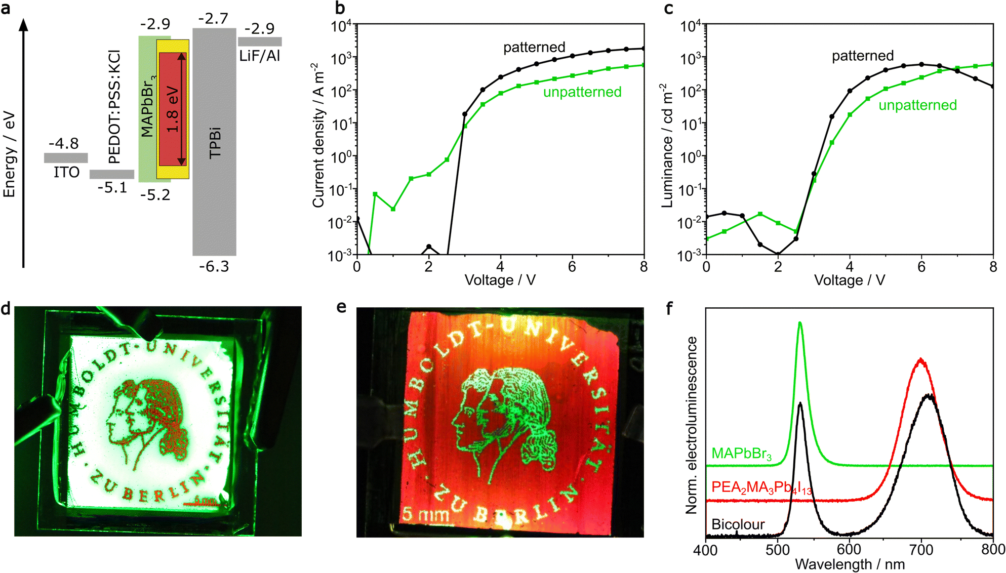 | ||
| Fig. 3 (a) The device architecture of fabricated PeLEDs with (b) current voltage and (c) luminance voltage characteristics of a pure green light emitting and patterned PeLED. (d) 400 mm2 devices with green background light emission and a red pattern or (e) red light emitting background layer and green light emitting pattern, by printing a negative image as pattern. The 5 mm scale bar is printed into the active layer. (f) Electroluminescence spectra of a bicoloured PeLED compared with the respective single-coloured devices. | ||
The current density–voltage (J–V) characteristics of a 20 × 20 mm device without printed pattern are compared to those of a bicoloured device in Fig. 3b. The patterned device shows a higher overall current density after turn-on. At voltage under 2 V, the current density remains low. Thus, the patterning process does not increase the leakage current by disrupting the perovskite layer integrity. Fig. 3c show the luminance–voltage (L–V) characteristics of both devices. Both devices show the same turn-on at 2.7 V (defined at 0.1 cd m−2) and a very comparable maximum luminance of 570 cd m−2. The luminance of the bicoloured device was measured in the background region to be comparable with the unpatterned device. Thus, the second printing step as such does not impact the device performance of the unpatterned regions.
The second printing step is controlled by a digital image that is fed into the inkjet printer software. This enables us to print arbitrary patterns, such as the logo of our university, in a PeLED with an active area of 400 mm2 (Fig. 3d) and 1600 mm2 (Fig. S2, ESI†). Even though the Br−-based perovskite forms the basis of the device operation, large area iodide-doping is also possible in order to invert the perceived image and create a red background with a green emission pattern (Fig. 3e). Fig. 3f displays the corresponding electroluminescence spectra. The narrow green light emission at 535 nm is well separated from the broader red light emission at 710 nm. Indicated as coloured areas are the emission spectra of single colour PeLEDs, fabricated with MAPbBr3:PEG and PEA2MA3Pb4I13, respectively. The red single-colour PeLED shows an emission at 700 nm, which is caused by PEA cations that shift the emission wavelength of MAPbI3 (∼780 nm) towards lower wavelengths.
Beyond the emission of red and green light, tri-coloured PeLEDs with a MAPbCl3 background layer could be realized for red, green, and blue (RGB) light emission from a single emitter layer. Due to the low performance of Cl−-based PeLEDs however, this approach is not promising.28,60 Thus, in further work we will utilize 2D and pseudo-2D MHPs to access blue light emitting PeLEDs. Tri-coloured PeLEDs could be achieved by selectively breaking the layered structure of a 2D perovskite background and shifting the wavelength of the printed pattern by reducing the quantum confinement towards green light emission. A third printing step for the creation of a mixed halide phase would enable red light emission for an RGB emitting device.
Conclusions
In this work, we demonstrated large area PeLEDs with bicolour light emission using an optimized high-resolution IJP process. In a sequential printing process, a primary, large area, Br−-based perovskite film was deposited and patterned with an I−-based perovskite ink. The dissolving and recrystallising process that took place during the second printing step achieved a minimum feature size of 100 μm. The created patterns contain a mixed-halide perovskite phase. Due to phase segregation in the mixed-halide perovskite and charge-carrier funnelling towards iodide-rich, low bandgap domains during operation, a red pattern on a green background is perceived. The two emission peaks at 535 nm and 710 nm are well separated and create a high visual contrast. By carefully controlling drop spacing and drying behaviour, large area PeLEDs with a clearly defined, readable, digitally based two-coloured emission pattern were fabricated, and can be used to display printed logos or printed signage. Beyond the use in bicoloured PeLEDs, the presented process will also allow the fabrication of other devices, such as (photo) detectors or transistors where spatially controlled lateral variation of the material composition is desired.Experimental
Perovskite ink preparation
The Br−-based perovskite ink (MAPbBr3:PEG, 0.125 M) was prepared in a nitrogen filled glovebox by dissolving lead bromide (>98%, TCI) and methyl ammonium bromide (99.99% trace elements basis, dyenamo) in a 3:7:10 mixture of DMF (anhydrous, 99.9%, Sigma-Aldrich), DMSO (anhydrous, >99.9%, Sigma-Aldrich) and GBL (>99.0%, TCI) to yield a 59.87 mg mL−1 (0.125 mol L−1) solution with an excess of 5 wt% of MABr. 8 mg mL−1 of PEG was added to this solution. The I−-based perovskite ink (PEA2MA3Pb4I13 0.031 M) was prepared in a similar way using a stoichiometric amount of lead iodide (>98%, TCI), methyl ammonium iodide (99% trace element basis, dyenamo) and phenethyl ammonium iodide (>98%, dyenamo) in a 3:1 mixture of GBL (>99.0%, TCI) and chlorobenzene (anhydrous, Sigma Aldrich).
Device fabrication
Patterned (25.4 × 25.4 mm2) and unpatterned (50 × 50 mm2) ITO substrates were purchased from Psiotec Limited. The 50 × 50 mm2 ITO substrates were patterned with a pulsed laser (1064 nm, 12 W) integrated in a PixDRO inkjet printer system. The substrates were cleaned with 1% Hellmanex III solution, followed by acetone and then isopropanol in an ultrasonic bath for 10 minutes each. The substrates were subsequently treated with oxygen plasma in a Femto plasma system (Diener). PEDOT:PSS (Al4083, Heraeus) was mixed with 5 mg L−1 KCl (Sigma Aldrich), filtered with a 0.45 μm PA filter and spin-coated at 1500 rpm for 12 s and 2500 rpm at 30 s. The PEDOT:PSS layers were annealed at 220 °C for 10 min before being transferred into a nitrogen filled glovebox. In the glovebox, the Br−-based perovskite ink was deposited with a PixDRO LP50 (Meyer-Burger/Suess) inkjet printer fitted with Spectra SE-128 print heads (30 pL nominal drop volume) and Dimatix cartridges (10 pL) with 350 dpi resolution. We note that the cartridges are damaged by the DMSO/DMF solvent system and cannot be reused multiple times. The films were dried in a specially developed aluminium chamber,16 by evacuating the chamber for 10 s, reaching a base pressure of ∼1 mbar. After evacuation, a valve was opened to allow and control the nitrogen flow over the substrate. The crystallization of the perovskite film was observed through a window in the chamber. After full crystallization, the substrate was transferred to a hotplate and annealed at 100 °C for 10 min. Afterwards, the printhead was swapped with a 1 pL Dimatix cartridge for the patterning step with PEA2MA3Pb4I13 ink. The patterns used in bicoloured PeLEDs were printed at 350 dpi. After the second printing step, the substrates were dried in the same aluminum chamber. Further annealing was not necessary. The substrates were transferred to another nitrogen filled glovebox fitted with a thermal evaporator. 20 nm TPBi, 1 nm LiF and 150 nm Al were thermally evaporated, with the overlap of ITO and aluminium electrode defining the active area of the devices. All devices were encapsulated using a commercially available epoxy (Blufixx) and hardened with a blue LED. The devices were characterized afterwards in ambient air.Thin film and device characterization
The PeLED devices were characterized by current density-luminance-voltage measurements using a Keithley source measurement unit 2612B, an LS160 luminance meter (Konica Minolta), a substrate holder and multiplexer (Ossila). Source measurement unit, multiplexer and candelameter were addressed with self-written software. The electroluminescence spectra were collected through an optical fibre with an HR 2000+ Ocean Optics spectrometer. UV-vis measurements were performed on a PerkinElmer Lambda 950 UV-vis spectrometer, whereby transmission was measured, and absorption was calculated accordingly. For the acquisition of PL spectra, samples were prepared by printing patterned perovskite layers on soda lime glass. A 420 nm laser with a spot size of 20 μm was used for the selective excitation of background and printed features.SEM images and EDX maps were collected with a Zeiss GeminiSEM 500. Samples were printed on ITO covered glass slides to electrically ground the samples during measurement. XRD experiments were performed on a Bruker Advanced D8 in Bragg–Brentano geometry under ambient conditions with a Cu Kα X-ray source (λ = 1.5406 Å).
Conflicts of interest
There are no conflicts of interest to declare.Acknowledgements
This work was carried out in the framework of the Joint Lab GEN_FAB and with the support of the Helmholtz Innovation Lab HySPRINT. The authors would like to thank Christoph T. Koch for granting instrument access. E. L. U. acknowledges funding from the German Ministry of Education and Research (BMBF) for the Young Investigator Group Hybrid Materials Formation and Scaling (HyPerFORME) within the program “NanoMatFutur” (Grant No. 03XP0091), as well as the Helmholtz Energy Materials Foundry (HEMF).Notes and references
- M. Jošt, L. Kegelmann, L. Korte and S. Albrecht, Adv. Energy Mater., 2020, 10, 1904102 CrossRef.
- M. Saliba, J. P. Correa-Baena, C. M. Wolff, M. Stolterfoht, N. Phung, S. Albrecht, D. Neher and A. Abate, Chem. Mater., 2018, 30, 4193–4201 CrossRef CAS.
- M. Jošt, T. Bertram, D. Koushik, J. A. Marquez, M. A. Verheijen, M. D. Heinemann, E. Köhnen, A. Al-Ashouri, S. Braunger, F. Lang, B. Rech, T. Unold, M. Creatore, I. Lauermann, C. A. Kaufmann, R. Schlatmann and S. Albrecht, ACS Energy Lett., 2019, 4, 583–590 CrossRef.
- E. Horváth, M. Spina, Z. Szekrényes, K. Kamarás, R. Gaal, D. Gachet and L. Forró, Nano Lett., 2014, 14, 6761–6766 CrossRef PubMed.
- J. Miao and F. Zhang, J. Mater. Chem. C, 2019, 7, 1741–1791 RSC.
- H. Wang, Y. Sun, J. Chen, F. Wang, R. Han, C. Zhang, J. Kong, L. Li and J. Yang, Nanomaterials, 2022, 12, 4390 CrossRef CAS PubMed.
- H. Wei and J. Huang, Nat. Commun., 2019, 10, 1–12 CrossRef PubMed.
- S. Yakunin, M. Sytnyk, D. Kriegner, S. Shrestha, M. Richter, G. J. Matt, H. Azimi, C. J. Brabec, J. Stangl, M. V. Kovalenko and W. Heiss, Nat. Photonics, 2015, 9, 444–449 CrossRef CAS PubMed.
- Y. C. Kim, K. H. Kim, D. Y. Son, D. N. Jeong, J. Y. Seo, Y. S. Choi, I. T. Han, S. Y. Lee and N. G. Park, Nature, 2017, 550, 87–91 CrossRef CAS PubMed.
- J. Li, L. Xu, T. Wang, J. Song, J. Chen, J. Xue, Y. Dong, B. Cai, Q. Shan, B. Han and H. Zeng, Adv. Mater., 2017, 29, 1603885 CrossRef PubMed.
- B. R. Lee, J. C. Yu, J. H. Park, S. Lee, C. K. Mai, B. Zhao, M. S. Wong, E. D. Jung, Y. S. Nam, S. Y. Park, D. Di Nuzzo, J. Y. Kim, S. D. Stranks, G. C. Bazan, H. Choi, M. H. Song and R. H. Friend, ACS Nano, 2018, 12, 5826–5833 CrossRef CAS PubMed.
- E. P. Yao, Z. Yang, L. Meng, P. Sun, S. Dong, Y. Yang and Y. Yang, Adv. Mater., 2017, 29, 1–7 Search PubMed.
- P. Du, J. Li, L. Wang, L. Sun, X. Wang, X. Xu, L. Yang, J. Pang, W. Liang, J. Luo, Y. Ma and J. Tang, Nat. Commun., 2021, 12, 1–10 CrossRef PubMed.
- J. Li, J. Dagar, O. Shargaieva, M. A. Flatken, H. Köbler, M. Fenske, C. Schultz, B. Stegemann, J. Just, D. M. Többens, A. Abate, R. Munir and E. Unger, Adv. Energy Mater., 2021, 11, 2003460 CrossRef CAS.
- V. Prakasam, D. Tordera, F. Di Giacomo, R. Abbel, A. Langen, G. Gelinck and H. J. Bolink, J. Mater. Chem. C, 2019, 7, 3795–3801 RSC.
- F. Mathies, E. R. Nandayapa, G. Paramasivam, M. F. Al Rayes, V. R. F. Schröder, C. Rehermann, E. J. W. List-Kratochvil and E. L. Unger, Mater. Adv., 2021, 2, 5365–5370 RSC.
- F. Mathies, E. J. W. List-Kratochvil and E. L. Unger, Energy Technol., 2020, 8, 1900991 CrossRef CAS.
- H. Näsström, O. Shargaieva, P. Becker, F. Mathies, I. Zizak, V. R. F. Schröder, E. J. W. List-Kratochvil, T. Unold and E. Unger, J. Mater. Chem. A, 2022, 10, 4906–4914 RSC.
- Y. Liu, F. Li, C. Perumal Veeramalai, W. Chen, T. Guo, C. Wu and T. W. Kim, ACS Appl. Mater. Interfaces, 2017, 9, 11662–11668 CrossRef CAS PubMed.
- S. Chen, L. Zhang, L. Yan, X. Xiang, X. Zhao, S. Yang and B. Xu, Adv. Funct. Mater., 2019, 29, 1905487 CrossRef CAS.
- F. Hermerschmidt, F. Mathies, V. R. F. Schröder, C. Rehermann, N. Z. Morales, E. L. Unger and E. J. W. List-Kratochvil, Mater. Horiz., 2020, 7, 1773–1781 RSC.
- V. R. F. Schröder, N. Fratzscher, F. Mathies, E. R. Nandayapa, F. Hermerschmidt, E. L. Unger and E. J. W. List-Kratochvil, Nanoscale, 2023, 5649–5654 RSC.
- Y. Zou, L. Cai, T. Song and B. Sun, Small Sci., 2021, 1, 2000050 CrossRef CAS.
- L. Liang, T. Ma, Z. Chen, J. Wang, J. Hu, Y. Ji, W. Shen and J. Chen, Adv. Mater. Technol., 2023, 8, 1–28 Search PubMed.
- H. Näsström, O. Shargaieva, P. Becker, F. Mathies, I. Zizak, V. R. F. Schröder, E. J. W. List-Kratochvil, T. Unold and E. L. Unger, J. Mater. Chem. A, 2022, 10, 4906–4914 RSC.
- V. R. F. Schröder, F. Hermerschmidt, S. Helper, C. Rehermann, G. Ligorio, H. Näsström, E. L. Unger and E. J. W. List-Kratochvil, Adv. Eng. Mater., 2021, 2101111, 1–7 Search PubMed.
- Q. Ou, X. Bao, Y. Zhang, H. Shao, G. Xing, X. Li, L. Shao and Q. Bao, Nano Mater. Sci., 2019, 1, 268–287 CrossRef.
- N. K. Kumawat, X. K. Liu, D. Kabra and F. Gao, Nanoscale, 2019, 11, 2109–2120 RSC.
- L. Cheng, Y. Cao, R. Ge, Y. Q. Wei, N. N. Wang, J. P. Wang and W. Huang, Chin. Chem. Lett., 2017, 28, 29–31 CrossRef CAS.
- G. Zou, Z. Li, Z. Chen, L. Chu, H. L. Yip and Y. Cao, Adv. Funct. Mater., 2021, 31, 2103219 CrossRef CAS.
- M. Yuan, L. N. Quan, R. Comin, G. Walters, R. Sabatini, O. Voznyy, S. Hoogland, Y. Zhao, E. M. Beauregard, P. Kanjanaboos, Z. Lu, D. H. Kim and E. H. Sargent, Nat. Nanotechnol., 2016, 11, 872–877 CrossRef CAS PubMed.
- H. Kim, W. Kim, Y. Pak, T. J. Yoo, H. W. Lee, B. H. Lee, S. Kwon and G. Y. Jung, Laser Photonics Rev., 2020, 14, 1–7 Search PubMed.
- K. Qasim, B. Wang, Y. Zhang, P. Li, Y. Wang, S. Li, S. T. Lee, L. S. Liao, W. Lei and Q. Bao, Adv. Funct. Mater., 2017, 27, 1606874 CrossRef.
- B. Han, Q. Shan, F. Zhang, J. Song and H. Zeng, J. Semicond., 2020, 41, 052205 CrossRef CAS.
- E. T. Hoke, D. J. Slotcavage, E. R. Dohner, A. R. Bowring, H. I. Karunadasa and M. D. McGehee, Chem. Sci., 2015, 6, 613–617 RSC.
- P. Vashishtha and J. E. Halpert, Chem. Mater., 2017, 29, 5965–5973 CrossRef CAS.
- C. Rehermann, A. Merdasa, K. Suchan, V. Schröder, F. Mathies and E. L. Unger, ACS Appl. Mater. Interfaces, 2020, 12, 30343–30352 CrossRef CAS PubMed.
- X. Tang, M. Van Den Berg, E. Gu, A. Horneber, G. J. Matt, A. Osvet, A. J. Meixner, D. Zhang and C. J. Brabec, Nano Lett., 2018, 18, 2172–2178 CrossRef CAS PubMed.
- H. Funk, O. Shargaieva, A. Eljarrat, E. L. Unger, C. T. Koch and D. Abou-Ras, J. Phys. Chem. Lett., 2020, 11, 4945–4950 CrossRef CAS PubMed.
- L. Tian, J. Xue and R. Wang, Electronics, 2022, 11, 1 Search PubMed.
- P. Gratia, G. Grancini, J. N. Audinot, X. Jeanbourquin, E. Mosconi, I. Zimmermann, D. Dowsett, Y. Lee, M. Grätzel, F. De Angelis, K. Sivula, T. Wirtz and M. K. Nazeeruddin, J. Am. Chem. Soc., 2016, 138, 15821–15824 CrossRef CAS PubMed.
- Y. Bai, Z. Huang, X. Zhang, J. Lu, X. Niu, Z. He, C. Zhu, M. Xiao, Q. Song, X. Wei, C. Wang, Z. Cui, J. Dou, Y. Chen, F. Pei, H. Zai, W. Wang, T. Song, P. An, J. Zhang, J. Dong, Y. Li, J. Shi, H. Jin, P. Chen, Y. Sun, Y. Li, H. Chen, Z. Wei, H. Zhou and Q. Chen, Science, 2022, 378, 747–754 CrossRef CAS PubMed.
- D. Di Girolamo, N. Phung, F. U. Kosasih, F. Di Giacomo, F. Matteocci, J. A. Smith, M. A. Flatken, H. Köbler, S. H. Turren Cruz, A. Mattoni, L. Cinà, B. Rech, A. Latini, G. Divitini, C. Ducati, A. Di Carlo, D. Dini and A. Abate, Adv. Energy Mater., 2020, 10, 2000310 CrossRef CAS.
- F. Lehmann, A. Franz, D. M. Többens, S. Levcenco, T. Unold, A. Taubert and S. Schorr, RSC Adv., 2019, 9, 11151–11159 RSC.
- M. Karlsson, Z. Yi, S. Reichert, X. Luo, W. Lin, Z. Zhang, C. Bao, R. Zhang, S. Bai, G. Zheng, P. Teng, L. Duan, Y. Lu, K. Zheng, T. Pullerits, C. Deibel, W. Xu, R. Friend and F. Gao, Nat. Commun., 2021, 12, 1–10 CrossRef PubMed.
- S. J. Yoon, M. Kuno and P. V. Kamat, ACS Energy Lett., 2017, 2, 1507–1514 CrossRef CAS.
- A. F. Gualdrón-Reyes, S. J. Yoon, E. M. Barea, S. Agouram, V. Muñoz-Sanjosé, Á. M. Meléndez, M. E. Niño-Gómez and I. Mora-Seró, ACS Energy Lett., 2019, 4, 54–62 CrossRef PubMed.
- F. Xu, D. Chen, D. Huang, K. Xu, S. Liang, J. Hu, X. Zhang, L. Liu, F. Xiong and H. Zhu, J. Phys. Chem. Lett., 2022, 13, 718–725 CrossRef CAS PubMed.
- J. Wang, D. Li, L. Mu, M. Li, Y. Luo, B. Zhang, C. Mai, B. Guo, L. Lan, J. Wang, H. L. Yip and J. Peng, ACS Appl. Mater. Interfaces, 2021, 13, 41773–41781 CrossRef CAS PubMed.
- J. Liang, Y. Du, K. Wang, A. Ren, X. Dong, C. Zhang, J. Tang, Y. Yan and Y. S. Zhao, Adv. Opt. Mater., 2022, 10, 1–8 CAS.
- J. Mao, H. Lin, F. Ye, M. Qin, J. M. Burkhartsmeyer, H. Zhang, X. Lu, K. S. Wong and W. C. H. Choy, ACS Nano, 2018, 12, 10486–10492 CrossRef CAS PubMed.
- Z. Chen, Z. Li, Z. Chen, R. Xia, G. Zou, L. Chu, S. J. Su, J. Peng, H. L. Yip and Y. Cao, Joule, 2021, 5, 456–466 CrossRef CAS.
- T. Guner and M. M. Demir, Phys. Status Solidi A, 2018, 215, 1–11 CrossRef.
- H. Yu, H. Wang, G. Pozina, C. Yin, X. K. Liu and F. Gao, Chem. Sci., 2020, 11, 11338–11343 RSC.
- C. Y. Chang, A. N. Solodukhin, S. Y. Liao, K. P. O. Mahesh, C. L. Hsu, S. A. Ponomarenko, Y. N. Luponosov and Y. C. Chao, J. Mater. Chem. C, 2019, 7, 8634–8642 RSC.
- L. Helmbrecht, M. H. Futscher, L. A. Muscarella, B. Ehrler and W. L. Noorduin, Adv. Mater., 2021, 33, 2005291 CrossRef CAS PubMed.
- A. Gao, J. Yan, Z. Wang, P. Liu, D. Wu, X. Tang, F. Fang, S. Ding, X. Li, J. Sun, M. Cao, L. Wang, L. Li, K. Wang and X. W. Sun, Nanoscale, 2020, 12, 2569–2577 RSC.
- M. Zhu, Y. Duan, N. Liu, H. Li, J. Li, P. Du, Z. Tan, G. Niu, L. Gao, Y. A. Huang, Z. Yin and J. Tang, Adv. Funct. Mater., 2019, 29, 1903294 CrossRef.
- C. F. Holder and R. E. Schaak, ACS Nano, 2019, 13, 7359–7365 CrossRef CAS PubMed.
- N. K. Kumawat, A. Dey, A. Kumar, S. P. Gopinathan, K. L. Narasimhan and D. Kabra, ACS Appl. Mater. Interfaces, 2015, 7, 13119–13124 CrossRef CAS PubMed.
Footnote |
| † Electronic supplementary information (ESI) available. See DOI: https://doi.org/10.1039/d3mh02025h |
| This journal is © The Royal Society of Chemistry 2024 |