
 Open Access Article
 This Open Access Article is licensed under a Creative Commons Attribution-Non Commercial 3.0 Unported Licence
3D simulation of conductive nanofilaments in multilayer h-BN memristors via a circuit breaker approach
D.
Maldonado
 a,
A.
Cantudo
a,
F. M.
Gómez-Campos
a,
Yue
Yuan
b,
Yaqing
Shen
b,
Wenwen
Zheng
b,
M.
Lanza
*b and
J. B.
Roldán
*a
a,
A.
Cantudo
a,
F. M.
Gómez-Campos
a,
Yue
Yuan
b,
Yaqing
Shen
b,
Wenwen
Zheng
b,
M.
Lanza
*b and
J. B.
Roldán
*a
aDepartamento de Electrónica y Tecnología de Computadores, Universidad de Granada, Facultad de Ciencias, Avd. Fuentenueva s/n, 18071 Granada, Spain. E-mail: jroldan@ugr.es
bMaterials Science and Engineering Program, Physical Sciences and Engineering Division, King Abdullah University of Science and Technology (KAUST), Thuwal 23955-6900, Saudi Arabia. E-mail: mario.lanza@kaust.edu.sa
First published on 2nd December 2023
Abstract
A 3D simulation of conductive nanofilaments (CNFs) in multilayer hexagonal-BN memristors is performed. To do so, a simulation tool based on circuit breakers is developed including for the first time a 3D resistive network. The circuit breakers employed can be modeled with two, three and four resistance states; in addition, a series resistance and a module to account for quantum effects, by means of the quantum point contact model, are also included. Finally, to describe real dielectric situations, regions with a high defect density are modeled with a great variety of geometrical shapes to consider their influence in the resistive switching (RS) process. The simulator has been tuned with measurements of h-BN memristive devices, fabricated with chemical-vapour-deposition grown h-BN layers, which were electrically and physically characterized. We show the formation of CNFs that produce filamentary charge conduction in our devices. Moreover, the simulation tool is employed to describe partial filament rupture in reset processes and show the low dependence of the set voltage on the device area, which is seen experimentally.
New conceptsIn this manuscript we present a new 3D memristor simulator based on circuit breakers (CBs). Previous simulators are 2D; therefore, it means a step forward in the description of memristor operation and the resistive switching processes. The CBs can be switched between different resistance values depending on the voltage between their terminals or on the CB temperature. By means of these mechanisms, which reflect the physics and chemistry involved in the operation of memristors, we are able to reproduce experimental data obtained in h-BN memristors and describe the conductive nanofilament formation and rupture that make the device operate. Moreover, we can reproduce reset processes where the current versus voltage curve presents several steps (partial nanofilament rupture). We can also describe defect regions in the dielectric (our simulation domain), allowing the study of pristine dielectrics and the corresponding resistive switching operation. The particularities of 2D materials (in this case, the dielectric of our devices is hexagonal boron nitride) have been considered in the simulator and they helped to understand the operation and experimental measurements of our devices. |
I. Introduction
Memristive devices have been intensively studied in Academia and industry in the last decade.1–3 These devices show great potential both for standalone and embedded non-volatile memory applications;4–8 in fact, they have already been incorporated in different industrial products.3 Their features make them fit the market needs (in general, as storage-class memory) and they are CMOS fabrication technology compatible (some memristive devices have a 4F2 footprint, where “F” is the minimum technology half-pitch).8Although memristor-based non-volatile memory applications are the most commercially advanced,9–11 these devices play an important role in other fields such as neuromorphic computing.12–21 The neuromorphic engineering approach22 allows the acceleration of matrix-vector multiplication (a key operation in Artificial Intelligence (AI) algorithms) that can be implemented through memristive device crossbar arrays.3,17 This approach can get over some of the hurdles of von Neumann's bottleneck, which are linked to the constant data movement between the memory and the processor. Memristive devices, in this neuromorphic computing context, mimic biological synapses to permit the fabrication of hardware neural networks.12–16,18–20,23 In this respect, due to the inherent redundancy of neural circuits, the device requirements do not need to be as strict as in non-volatile memory applications since AI methodologies allow a greater margin of variability and endurance.17
Resistive switching memristors are fabricated with a thin layer of dielectric sandwiched between metal electrodes; their electrical and thermal features are closely linked to the materials employed. Different authors have described switching and charge conduction making use of the dynamics of metallic ions, oxygen vacancies and other defects, whose concentration evolves with time in the device active part.24–30 In particular, for filamentary conduction, the formation and destruction of CNFs is a stochastic process that leads to cycle-to-cycle (C2C) variability.6,7,31–33 This inherent variability (in addition to device-to-device (D2D) variability31) has to be minimized for memory applications; however, it could be beneficial in some cases for deep neural network training to avoid overfitting.34 Variability is key for hardware cryptography (an entropy source that allows the fabrication of physical unclonable functions and random number generators).35–39 C2C variability is linked to CNF morphological changes in each RS cycle, where the CF is created (set process) and ruptured (reset process) successively.24–26,29,30 The device C2C and D2D variability, and switching dynamics can be tackled from different simulation and modeling approaches, such as kinetic Monte Carlo (kMC) simulation,24,26,28,40,41 advanced statistical modeling42,43 and compact modeling (for circuit simulation and design).2,44–50 A different approach, although complementary, is based on RRAM simulation by means of circuit breakers (CB).7,51–56 These CB-based simulators are bidimensional; nevertheless, a 3D approach is needed if CNFs (in the case of filamentary operation) are to be described correctly, see ref. 57 for a study on the appropriateness of a 3D description in comparison with a 2D approach based on a kMC simulation tool. CB-based simulation poses a numerical technique in between kMC and compact modeling for circuit simulation in what is referred to as complexity, although it allows a reasonable description of variability and current versus voltage curves.
In this work, we present a 3D CB-based simulator that can describe the CNF evolution (that facilitates RS operation) and the charge transport in the filamentary operation regime. Apart from common features for these CB-based simulation tools,7,51–54 we include quantum effects implemented through the quantum point contact model, the use of circuit breakers with four conductivity stages and a device series resistance. We also consider 3D regions of different shapes within the simulator domain to model dielectric zones with high defect density formed at the fabrication stage that evolve as the RS unfolds. This latter feature is hardly ever taken into consideration in simulation tools.
We have tuned our simulator making use of experimental measurements from hexagonal boron-nitride memristive devices58 that we have fabricated. The devices characterized here have been studied previously,18,59 and physical and electrical experimental characterization was employed. Devices with some similarities in the layer stack were also analyzed from different viewpoints.60 All these works were purely experimental. In this work, we present an analysis where a strong simulation approach was introduced. The 3D modeling employed was implemented by means of a new CB-based simulator that allows the assessment of different physical effects on the RS operation and the role of high defect density regions in the dielectric on device variability and reliability.
It is important to draw attention to the fact that there exist different physical characterization techniques to visualize conductive nanofilaments.61–63 They are based on the use of conductive atomic force microscopy (C-AFM) and transmission electron microscopy (TEM). These techniques allow outstanding analyses that give us information about the CNF composition, size, shape, charge transport features, etc. This information can be used in the development of models and simulation tools. They are also important for the model and simulator calibration, in addition to electrical measurements. Once the simulators are tuned, they can complement C-AFM and TEM by providing an exact map of the temperature and the electric field in the simulation domain (usually the dielectric, although it could include the electrodes), the progress in the CNF formation, the influence of high defect density regions on RS, quantum effects, and charge transport processes.
The measurements have been correctly fitted and different operational particularities have been explained in full. In particular, in Section II, we introduce the fabrication and measurement details; the simulator description is presented in Section III and the results and discussion is given in Section IV. Finally, the main conclusions are drawn in Section V.
II. Device fabrication and measurement setup
The memristive devices used in our study have been introduced previously.18 The electrodes are made of a bilayer of 40 nm Au/10 nm Ti (E-beam evaporation is employed). The bottom electrode is deposited on a Si wafer, with 300 nm SiO2 on top of the Si. Then, a h-BN multilayer (18 layers approximately, see Fig. 1a and b) film was placed on top of the bottom electrode by wet transfer from a Cu foil where it was grown by chemical vapor deposition. In Fig. 1c, RS I–V curves are shown. They are obtained with a B1500A Keysight semiconductor parameter analyzer and a probe station (Karl Suss); ramped voltage stress (RVS) is used for the measurement of long RS series with consecutive set and reset cycles. RS operation is filamentary.18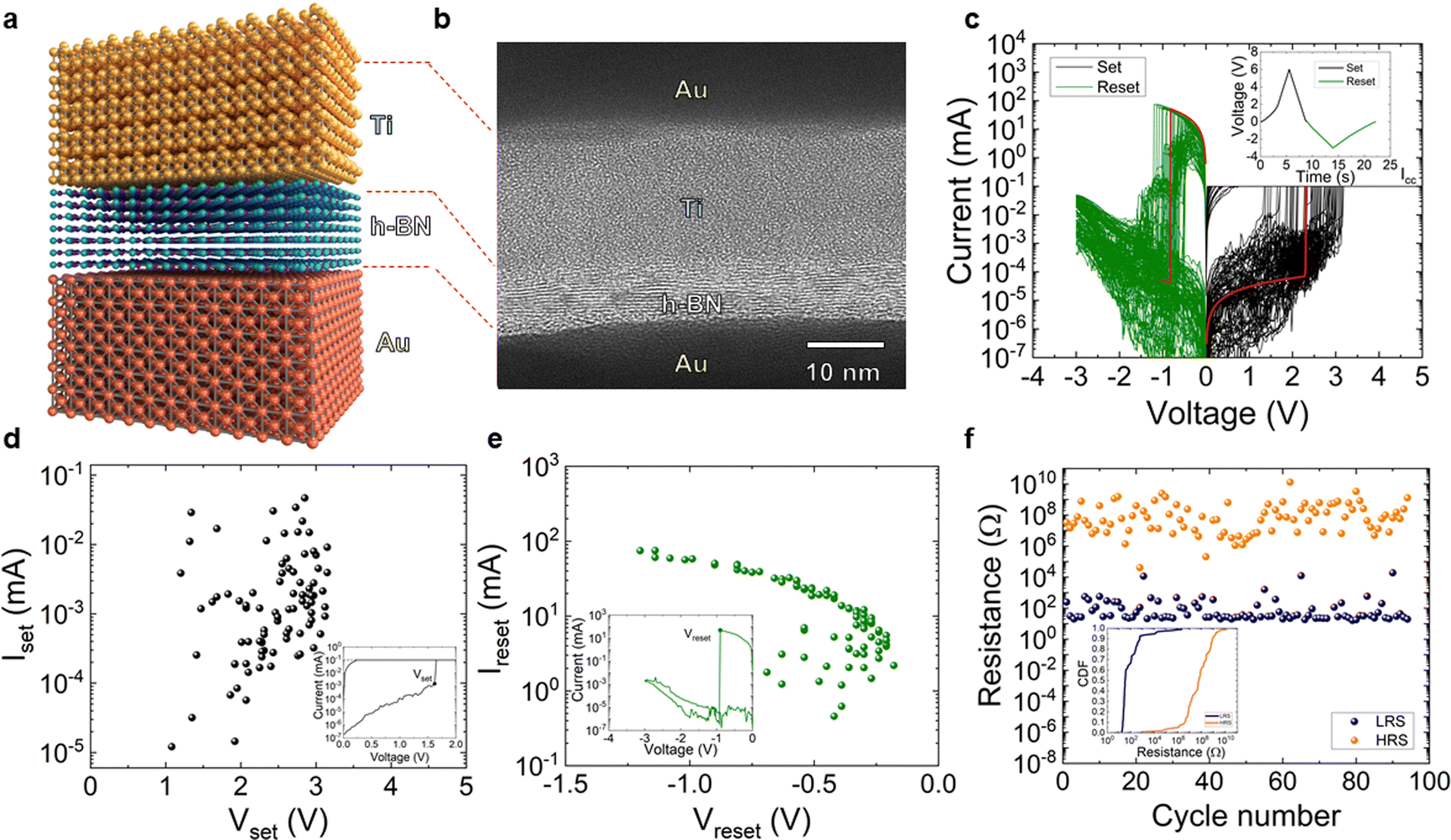 | ||
| Fig. 1 (a) Device layer scheme, (b) cross-section TEM image of the dielectric and surrounding layers in the device stack. In the h-BN dielectric, we have approximately 18 layers that were transferred from Cu foils. (c) Current versus voltage measured in the ramped voltage stress operation regime; see the voltage versus time signal in the inset. (d) Set current versus set voltage for the curves shown in (c); the set point definition is shown in the inset. (e) Reset current versus voltage for the I–V curves in (c); in the inset is shown the criterion established to define the reset voltage. (f) HRS and LRS resistance values versus cycle number in the resistive switching series obtained in (c) (the data are read at 0.1 V). Inset: Cumulative distribution function (CDF) of the HRS and LRS resistance values. | ||
In Fig. 1d and e, we plot the set and reset parameters, and the low and high resistance states (LRS/HRS) are plotted in Fig. 1f. It is clear that the resistance ratio (RHRS/RLRS) allows non-volatile memory applications (see the cumulative distribution functions of RHRS and RLRS in the inset in Fig. 1f, a reasonable variability is obtained).
It is interesting to highlight that CVD grown polycrystalline h-BN multilayers, such as the one employed here, work well for RS devices since they include insulating 2D layered regions and clusters of defects that are more conductive (these clusters of defects may be related to lattice distortions that propagate from one layer to another60,64). Other options, such as exfoliated h-BN, do not exhibit RS.65
III. Simulator description
The simulation tool that we developed, based on CBs, allows the analysis of RRAM RS, charge conduction and variability. CNF creation and destruction can be modeled to describe both unipolar and bipolar device operations. A 3D approach is followed, and therefore, it means a step forward with respect to 2D CB tools7,51–55 (see Fig. 2a). Following the simulation scheme unfolded in ref. 55, CBs with several conductance levels are included (Fig. 2b). Quantum effects in the charge conduction are considered by means of the quantum point contact (QPC) model,66,67 also the effects of metal pads and electrodes are included through a series resistance68 (Fig. 2a).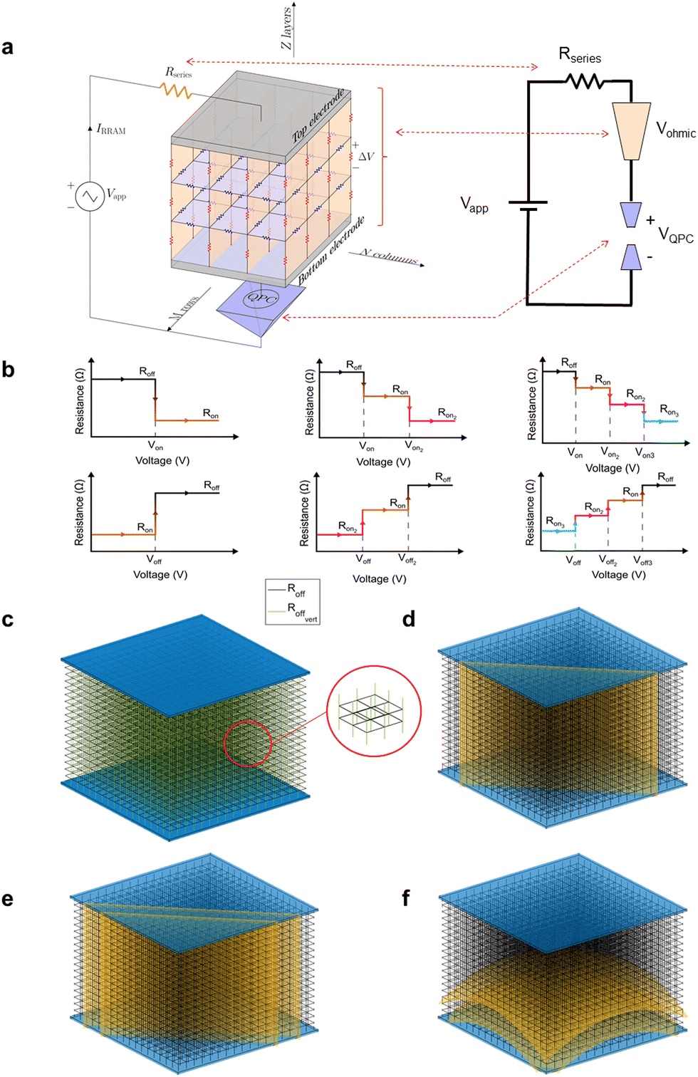 | ||
| Fig. 2 (a) Schematics of the 3D CB network diagram that depicts the internal electric circuitry included in the simulator to model the device. The horizontal CBs symbolize B vacancies embedded within the percolation path. The CBs are differentiated by blue and red colors, describing conduction in the h-BN layers (with lower associated resistances) and in the perpendicular direction of the BN planes (corresponding to much higher resistance in our model). The top and bottom electrodes are connected to an external voltage source. The model includes a series resistance that accounts for the metal pads and electrode resistances, and it is obviously in series with the resistance network that represents the dielectric. Quantum effects related to potential barriers along the charge conduction path are taken into consideration by means of the QPC model. A single module for the QPC model is employed in series with the resistance network. (b) The CB internal resistance values for the set (or forming) process are categorized into two levels (Roff and Ron), three levels (Roff, Ron, and Ron2) and four levels (Roff, Ron, Ron2, and Ron3). Similarly, for the reset process, the CB internal resistance structure is described for two, three or four levels. (c) Schematic of the 3D CB network incorporating two types of CBs to address the resistivity in-layer and out-of-layer in the h-BN. In this case, the horizontal CBs are represented in black, while the vertical CBs are denoted in green to better visualize them. (d) 3D CB network including a 2D vertical plane (in yellow) to model a region with a higher defect density, (e) 3D vertical plane and (f) a 3D curved plane in the CB domain to represent regions of different shapes with a higher defect density. | ||
The particularities of the h-BN dielectric are considered by utilizing two types of CB resistance values: in-plane CBs, represented in blue in Fig. 2a, that account for charge conduction in the BN layers, and out-of-plane CBs (red ones) that represent charge conduction in the dielectric vertical direction. The resistance values are described as plotted in Fig. 2b, selecting two, three or four levels. In whatever case, the red CBs are scaled with respect to the blue ones due to the different nature of the transport in a h-BN plane or in the perpendicular direction of the multilayer stack (c-axis).
At the beginning of the simulation (corresponding to a pristine dielectric), we can select the probability of having some CBs in the low resistance values (in case of two levels, the Ron value) in all the dielectric volume. In addition, we can define a 3D region, described by its geometrical equation, where the probability of having defects is higher than in the rest of the dielectric (this is modeled by increasing the CB probability of being in the low resistance value at the beginning of the simulation). Within the regions selected, determining a certain geometry (a single plane, Fig. 2d, a thick plane Fig. 2e, including several layers of CBs; a curved surface of different thickness, Fig. 2f), the initial probability can be changed (usually higher) with respect to the rest of the dielectric. This assumption can help to consider different pristine dielectrics or changes along a switching cycle series, and, therefore, direct the CNF formation through this region. If we consider three or four resistance levels for each CB, we can also select between other low resistance levels (Ron, Ron2, Ron3) as the CNF is getting formed along a set or forming process. The CB high-resistance component represents a defect-free dielectric region where charge transport is not enhanced by any means and the h-BN works as an ideal dielectric. The CB low-resistance component could be associated with the presence of a Ti atom inside the h-BN stack. TiX+ ions move toward the cathode across the dielectric leading to CNF formation through the h-BN multilayer. These CNFs short the electrodes and strongly reduce the device resistance. The ions are expected to diffuse preferentially at locations where the lower density of the material and the larger density of B and N vacancies favor their migration. Under negative bias (the bottom electrode is assumed to be always grounded), TiX+ ions may diffuse back to their original positions leading to CNF rupture, i.e., a reset event.18,60
The switching between the CB resistance values is performed when Von (also Von1 and Von2) or Voff (also Voff1 and Voff2) are overpassed (see Fig. 2b). Additionally, a fully thermal simulation can be performed by controlling the CB switching through temperature calculations, as described in ref. 55 and 69.
IV. Results and discussion
We have simulated the devices described in Section II. An 18 × 18 × 18 matrix of resistors was employed since the 6 nm-thick dielectric consists of 18 layers approximately of h-BN.16,18 We have employed a two-value CB resistance model, although higher complexities are allowed in the simulation tool (see Fig. 2b). As a reference, the scale between the values of the blue (in-plane CBs), see Fig. 2a, and red (out-plane CBs, higher resistance) resistances assumed in the simulation was 10. In this case, the best fit of the experimental curve was performed (blue curve, Fig. 3a and b). For a scale factor of 20 the green curve for the set I–V curve is obtained (Fig. 3a and b). We have also included for the sake of comparison a simulation where no distinction between the horizontal and vertical CBs is assumed (orange curve corresponding to CBs with equal resistance values). In this latter case a very different I–V curve is obtained. Due to the h-BN material structure, a distinction between in-plane and out-of-plane CBs is needed.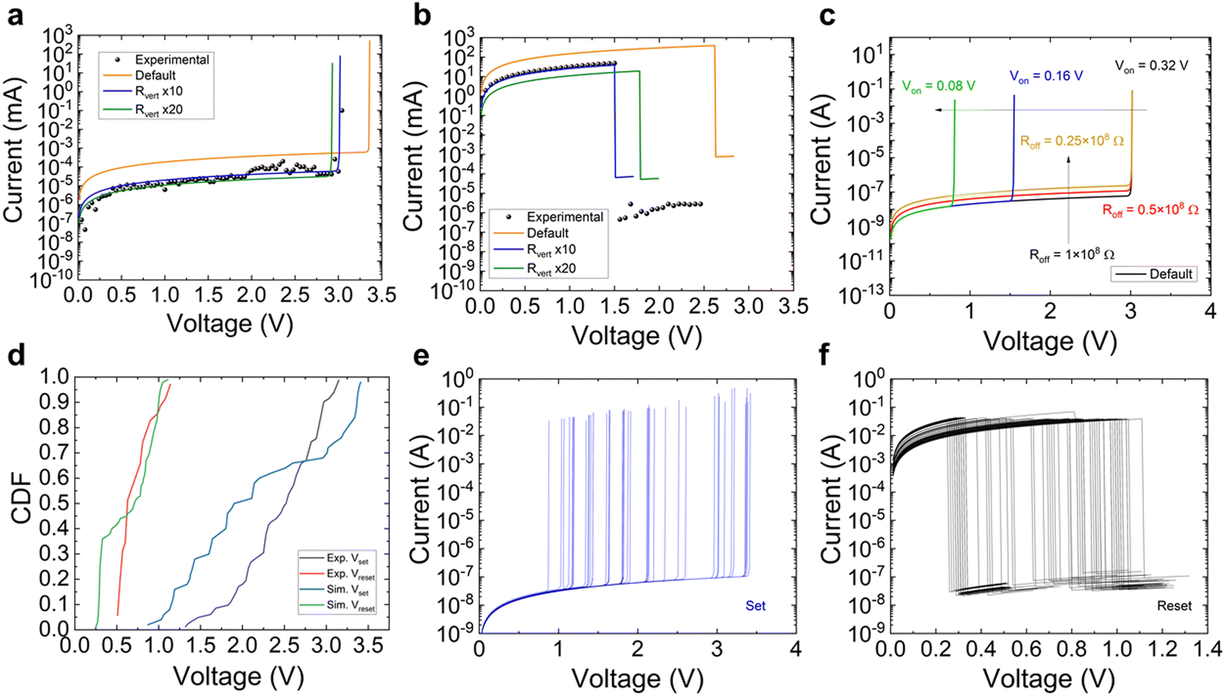 | ||
| Fig. 3 (a) Current versus voltage absolute value curve of simulated data (solid lines) and experimental data (black symbols) for a set process and (b) for a reset process. An 18 × 18 × 18 resistor array was employed to obtain this simulation using CBs with two resistance levels: Roff = 1 × 10⁸ Ω and Ron = 0.5 Ω. The model parameters in relation to Fig. 2 are: Voff = 0.195 V and Von = 0.32 V. A 10 scale factor was employed between horizontal (lower) and vertical (higher) resistances. This corresponds to the blue line, a scale factor of 20 was used in the green line. The default curve (orange) stands for CBs with similar resistance values for the vertical and horizontal directions. (c) Simulated current versus voltage set curves. The model parameters employed were those of panel a, for the default curve. Other curves obtained by changing some of the model parameters are shown for comparison, to assess their influence in the simulation tool. (d) CDFs for the experimental (c) and simulated (panels e and f) set and reset voltage (absolute value) points extracted from the I–V curves. (e) and (f) Simulated set (reset) cycles obtained for different probabilities for the defect density included in the geometry described in Fig. 2e (a thick plane). The simulation parameters are the same as in Fig. 3a and b. Voltage absolute values were considered for the reset processes. | ||
The fitting of the I–V experimental curves is shown in Fig. 3a and b. Some simulated curves are shown in Fig. 3c for different model parameters. See how the current level and the set voltage depend on the model parameters. A comparison between the set and reset voltage CDFs obtained from experimental and simulated curves is given in Fig. 3d. The group of simulated curves is obtained by changing the thickness of the geometry shown in Fig. 2e, and the probability linked to the CBs within this geometry in the low resistance state at the beginning of the simulation (see Fig. 3e and f where the group of simulated I–V curves is shown). In spite of the approximations performed in the modeling implemented in the simulator, the curve fitting is reasonable (Fig. 3d). In this respect the cycle-to-cycle variability can be described with our simulation tool.
In Fig. 4a we have plotted a simulated set current versus voltage. Different points have been marked along the curve in order to follow the CNF evolution. The low resistance value circuit breakers (Ron) are shown in red in Fig. 4b–e (assuming two resistance values CBs); these panels correspond to the simulation points shown in symbols in Fig. 4a. Notice how the CNF is formed as the set process unfolds until (in Fig. 4e) it shorts the electrodes and constitutes a fully-formed conduction path. The latter points (2–4) correspond to the sudden current rise that is seen both in simulated and experimental curves close to the set point, where a positive feedback process linked to the CNF formation is triggered.24
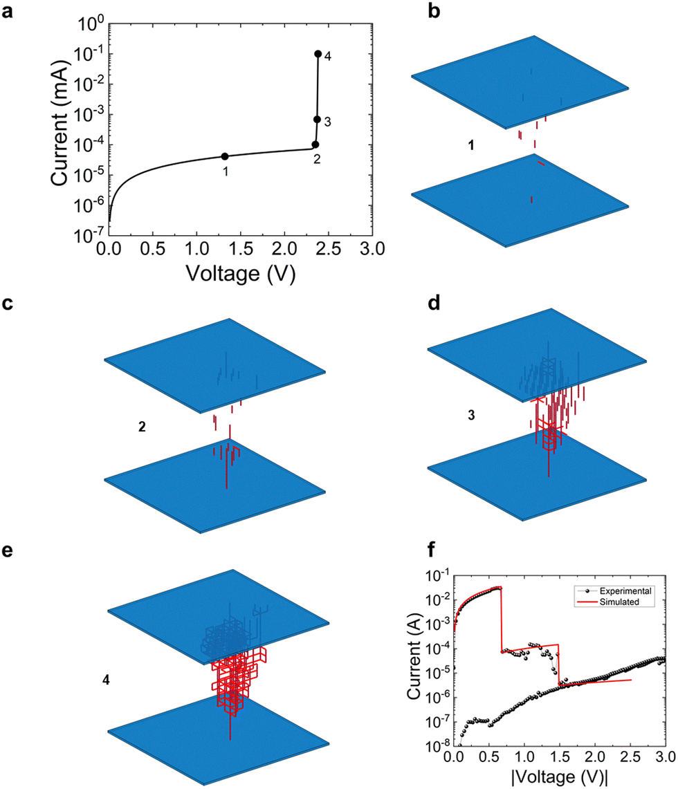 | ||
| Fig. 4 (a) Simulated current versus voltage in a set process. See different points along the I–V that correspond to different CNF formation stages (the CNFs are plotted in panels (b)–(e)). An 18 × 18 × 18 network was employed to obtain this simulation using CBs with two resistance levels: Roff = 65.5 × 10⁶ Ω, Ron = 0.24 Ω. The model parameters in relation with Fig. 2 are: Voff = 0.11 V, Von = 0.25 V. A 10 scale factor was employed between horizontal (lower) and vertical (higher) resistances. (f) Simulated and experimental current versus voltage in a set process. A clear stepped curve is seen due to the partial CNF rupture along the reset process. | ||
Some of the experimental curves measured present a stepped-like shape (see Fig. 4f) due to a CNF rupture in several stages. Our simulator can reproduce this behavior. In this respect, a single CNF could be broken in steps, or two CNFs (formed in a previous set event) can go through a reset process and get broken at different times. Experimental and simulated curves are shown in Fig. 4f to illustrate this effect.
The simulator can also be used to study large area devices. For instance, 100 nm × 100 nm area devices are simulated maintaining the number of CBs per nanometer that corresponds to the description of the h-BN layers of the dielectric described above. In this respect, millions of CBs are taken into consideration (see Fig. 5a and b for plots of a large area device simulation CB network). In this case, big matrix processing acceleration techniques have been implemented. In Fig. 5c we have shown arbitrary I–V curves simulated for devices with different areas. In this case no regions of high defect density were assumed. The probability of finding CBs in the low resistance value at the beginning of the simulation (1% in these examples) was the same in all cases; notice that a different random distribution is generated at the start of each simulation. We have scaled the I–V curves by a factor Areasmallest_area_simulated/Areaactual_device_area in order to fairly compare the curves taking into consideration the purely resistive network that we have employed to model the device. It is seen that, although the current curves are close together, the set voltage varies in each of the device areas employed. This parameter depends on the initial random distribution of low resistance CBs. We have plotted the set voltage versus device area in Fig. 5d, and it can be seen that as the area increases the set voltage decreases. This effect is linked to the higher probability (for the higher area devices) of finding a pre-formed subpath with the random initial CB configuration to let the CNF be created. As can be seen, as the area increases, the set voltage reduction saturates, as it is expected for devices where charge conduction is based on filamentary switching (Fig. 5d).
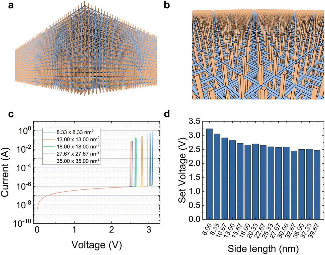 | ||
| Fig. 5 (a) Resistance network corresponding to a great area (100 nm × 100 nm) device. (b) Resistance network corresponding to a great area (100 nm × 100 nm) device (zoomed-in view). (c) Several simulated set I–V curves for different device areas (the current values are scaled with respect to the lowest area shown in the plot, i.e. (8.33 nm × 8.33 nm)). (d) Set voltage versus device side length (assuming a device square area obtained as (side length)2). | ||
V. Conclusions
A 3D simulation tool based on CBs is developed for the first time to describe RS in multilayer h-BN memristors. It is based on CBs that can be modeled with two, three and four resistance states; in addition, a series resistance and a module are included to account for quantum effects. The simulator has been tuned with measurements of h-BN memristive devices. The influence of the model parameters has been shown in the simulator tuning process. We also show the CNF formation that accounts for filamentary charge conduction in our devices, explaining the current abrupt change when the set event takes place. In doing so, the particularities of the material have been taken into consideration. Moreover, the simulation tool is employed to describe partial filament rupture in reset processes. Finally, the dependence of the set voltage with the device area is described by means of simulations with a massive number of CBs.Data available on request from the authors
The data that support the findings of this study are available from the corresponding author upon reasonable request.Conflicts of interest
There are no conflicts of interest to declare.Acknowledgements
We acknowledge project PID2022-139586NB-44 funded by MCIN/AEI/10.13039/501100011033 and by the European Union NextGenerationEU/PRTR. F. M. G.-C. thanks project PP2022.PP-13 funded by “Ayudas del Plan Propio UGR 2022”. M. L. acknowledges generous support from the King Abdullah University of Science and Technology.References
- L. O. Chua and S. M. Kang, Memristive devices and systems, Proc. IEEE, 1976, 64(2), 209–223 Search PubMed.
- F. Corinto, P. P. Civalleri and L. O. Chua, A Theoretical Approach to Memristor Devices, IEEE J. Emerging Selected Top. Circuits Syst., 2015, 5(2), 123–132 Search PubMed.
- M. Lanza, A. Sebastian, W. D. Lu, M. Le Gallo, M. F. Chang, D. Akinwande, F. M. Puglisi, H. N. Alshareef, M. Liu and J. B. Roldan, Memristive technologies for data storage, computation, encryption, and radio-frequency communication, Science, 2022, 376(6597), eabj9979 CrossRef CAS PubMed.
- F. Pan, S. S. Gao, C. Chen, C. Song and F. Zeng, Recent progress in resistive random access memories: Materials, switching mechanisms, and performance, Mater. Sci. Eng., R, 2014, 83, 1–59 CrossRef.
- M. Lanza, H.-S. Philip Wong, E. Pop, D. Ielmini, D. Strukov and B. Regan, et al., Recommended Methods to Study Resistive Switching Devices, Adv. Electron. Mater., 2019, 5(1), 1800143 CrossRef.
- D. Ielmini and R. Waser, Resistive Switching: From Fundamentals of Nanoionic Redox Processes to Memristive Device Applications, Wiley eBooks, 2016 Search PubMed.
- J. S. Lee, S. Lee and T. W. Noh, Resistive switching phenomena: A review of statistical physics approaches, Appl. Phys. Rev., 2015, 2(3), 031303 Search PubMed.
- S. Spiga, A. Sebastian, D. Querlioz and B. Rajendran, Memristive Devices for Brain-Inspired Computing, Elsevier eBooks, Elsevier, 2020 Search PubMed.
- C. C. Yang, C. Wu, M. Yang, W. Wang, M. Yang, T. C. Chien, et al.Industrially Applicable Read Disturb Model and Performance on Mega-Bit 28nm Embedded RRAM, Proceedings of the IEEE Symposium, 2020 Search PubMed.
- C. C. Chou, Z. J. Lin, C. M. Lai, C. J. Su, P. L. Tseng, W. C. Chen, et al.A 22nm 96KX144 RRAM Macro with a Self-Tracking Reference and a Low Ripple Charge Pump to Achieve a Configurable Read Window and a Wide Operating Voltage Range, Proceedings of the IEEE Symposium on VLSI Circuits, 2020 Search PubMed.
- C. C. Chou, Z. J. Lin, P. L. Tseng, C. F. Li, C. S. Chang, W. C. Chen, et al.An N40 256K×44 embedded RRAM macro with SL-precharge SA and low-voltage current limiter to improve read and write performance, Proceedings of the IEEE International Solid-State Circuits Conference (ISSCC), 2018 Search PubMed.
- S. Yu, Y. Wu, R. Jeyasingh, D. Kuzum and H. S. P. Wong, An Electronic Synapse Device Based on Metal Oxide Resistive Switching Memory for Neuromorphic Computation, IEEE Trans. Electron Devices, 2011, 58(8), 2729–2737 CAS.
- S. Ambrogio, P. Narayanan, H. Tsai, R. M. Shelby, I. Boybat and C. di Nolfo, et al., Equivalent-accuracy accelerated neural-network training using analogue memory, Nature, 2018, 558(7708), 60–67 CrossRef CAS PubMed.
- P. A. Merolla, J. V. Arthur, R. Alvarez-Icaza, A. S. Cassidy, J. Sawada and F. Akopyan, et al., Artificial brains. A million spiking-neuron integrated circuit with a scalable communication network and interface, Science, 2014, 345(6197), 668–673 CrossRef CAS PubMed.
- F. Alibart, E. Zamanidoost and D. B. Strukov, Pattern classification by memristive crossbar circuits using ex situ and in situ training, Nat. Commun., 2013, 4(1), 2072 CrossRef PubMed.
- K. Zhu, S. Pazos, F. Aguirre, Y. Shen, Y. Yuan and W. Zheng, et al., Hybrid 2D/CMOS microchips for memristive applications, Nature, 2023, 618(7963), 57–62 CrossRef CAS PubMed.
- A. Sebastian, M. Le Gallo, R. Khaddam-Aljameh and E. Eleftheriou, Memory devices and applications for in-memory computing, Nat. Nanotechnol., 2020, 15(7), 529–544 CrossRef CAS PubMed.
- J. B. Roldan, D. Maldonado, C. Aguilera-Pedregosa, E. Moreno, F. Aguirre and R. Romero-Zaliz, et al., Spiking neural networks based on two-dimensional materials, npj 2D Mater. Appl., 2022, 6(1), 63 CrossRef.
- M. Prezioso, F. Merrikh-Bayat, B. D. Hoskins, G. C. Adam, K. K. Likharev and D. B. Strukov, Training and operation of an integrated neuromorphic network based on metal-oxide memristors, Nature, 2015, 521(7550), 61–64 CrossRef CAS.
- M. A. Zidan, J. P. Strachan and W. D. Lu, The future of electronics based on memristive systems, Nat. Electron., 2018, 1(1), 22–29 CrossRef.
- F. Hui, P. Liu, S. A. Hodge, T. Carey, C. Wen and F. Torrisi, et al., In Situ Observation of Low-Power Nano-Synaptic Response in Graphene Oxide Using Conductive Atomic Force Microscopy, Small, 2021, 2101100 CrossRef CAS.
- C. Mead and M. Ismail, Analog VLSI Implementation of Neural Systems, The Kluwer International Series in Engineering and Computer Science, Springer US, Boston, MA, 1989 Search PubMed.
- T. Dalgaty, N. Castellani, C. Turck, K. E. Harabi, D. Querlioz and E. Vianello, In situ learning using intrinsic memristor variability via Markov chain Monte Carlo sampling, Nat. Electron., 2021, 4(2), 151–161 CrossRef.
- S. Aldana, P. García-Fernández, R. Romero-Zaliz, M. B. Gonzalez, F. Jiménez-Molinos and F. M. Gómez-Campos, et al., Resistive switching in HfO2 based valence change memories, a comprehensive 3D kinetic Monte Carlo approach, J. Phys. D: Appl. Phys., 2020, 53(22), 225106 CrossRef CAS.
- M. von Witzleben, K. Fleck, C. Funck, B. Baumkötter, M. Zuric and A. Idt, et al., Investigation of the Impact of High Temperatures on the Switching Kinetics of Redox-Based Resistive Switching Cells using a High-Speed Nanoheater, Adv. Electron. Mater., 2017, 3(12), 1700294 CrossRef.
- S. Dirkmann, J. Kaiser, C. Wenger and T. Mussenbrock, Filament Growth and Resistive Switching in Hafnium Oxide Memristive Devices, ACS Appl. Mater. Interfaces, 2018, 10(17), 14857–14868 CrossRef CAS PubMed.
- M. Bocquet, D. Deleruyelle, H. Aziza, C. Muller, J. M. Portal and T. Cabout, et al., Robust Compact Model for Bipolar Oxide-Based Resistive Switching Memories, IEEE Trans. Electron Devices, 2014, 61(3), 674–681 CAS.
- S. Aldana, E. Pérez, F. Jiménez-Molinos, C. Wenger and J. B. Roldán, Kinetic Monte Carlo analysis of data retention in Al:HfO2-based resistive random access memories, Semicond. Sci. Technol., 2020, 35(11), 115012 CrossRef CAS.
- S. Menzel, P. Kaupmann and R. Waser, Understanding filamentary growth in electrochemical metallization memory cells using kinetic Monte Carlo simulations, Nanoscale, 2015, 7(29), 12673–12681 RSC.
- C. Funck and S. Menzel, Comprehensive Model of Electron Conduction in Oxide-Based Memristive Devices, ACS Appl. Electron. Mater., 2021, 3(9), 3674–3692 CrossRef CAS.
- E. Pérez, D. Maldonado, C. Acal, J. E. Ruiz-Castro, F. Alonso and A. Aguilera, et al., Analysis of the statistics of device-to-device and cycle-to-cycle variability in TiN/Ti/Al:HfO2/TiN RRAMs, Microelectron. Eng., 2019, 214, 104–109 CrossRef.
- A. N. Mikhaylov, D. V. Guseinov, A. I. Belov, D. S. Korolev, V. A. Shishmakova and M. N. Koryazhkina, et al., Stochastic resonance in a metal-oxide memristive device, Chaos, Solitons Fractals, 2021, 144, 110723 CrossRef.
- J. B. Roldan, E. Miranda, D. Maldonado, A. N. Mikhaylov, N. V. Agudov and A. A. Dubkov, et al., Variability in Resistive Memories, Adv. Intell. Syst., 2023, 2200338 CrossRef.
- R. Romero-Zaliz, E. Perez, F. Jiménez-Molinos, C. Wenger and J. B. Roldán, Study of Quantized Hardware Deep Neural Networks Based on Resistive Switching Devices, Conventional versus Convolutional Approaches, Electronics, 2021, 10(3), 346 CrossRef CAS.
- R. Carboni and D. Ielmini, Stochastic Memory Devices for Security and Computing, Adv. Electron. Mater., 2019, 5(9), 1900198 CrossRef.
- S. Pazos, W. Zheng, T. Zanotti, F. Aguirre, T. E. Becker and Y. Shen, et al., Hardware implementation of a true random number generator integrating a hexagonal boron nitride memristor with a commercial microcontroller, Nanoscale, 2023, 15(5), 2171–2180 RSC.
- Z. Wei, Y. Katoh, S. Ogasahara, Y. Yoshimoto, K. Kawai, Y. Ikeda, et al.True random number generator using current difference based on a fractional stochastic model in 40-nm embedded ReRAM, IEEE International Electron Devices Meeting (IEDM), 2016 Search PubMed.
- A. Chen, Utilizing the Variability of Resistive Random Access Memory to Implement Reconfigurable Physical Unclonable Functions, IEEE Electron Device Lett., 2015, 36(2), 138–140 Search PubMed.
- C. Wen, X. Li, T. Zanotti, F. M. Puglisi, Y. Shi and F. Saiz, et al., Advanced Data Encryption using 2D Materials, Adv. Mater., 2021, 33(27), 2100185 CrossRef CAS.
- A. Padovani, P. Lugli, O. Pirrotta, L. Vandelli and G. Bersuker, Microscopic Modeling of HfOx RRAM Operations: From Forming to Switching, IEEE Trans. Electron Devices, 2015, 62(6), 1998–2006 CAS.
- J. Guy, G. Molas, P. Blaise, M. Bernard, A. Roule and G. Le Carval, et al., Investigation of Forming, SET, and Data Retention of Conductive-Bridge Random-Access Memory for Stack Optimization, IEEE Trans. Electron Devices, 2015, 62(11), 3482–3489 Search PubMed.
- J. B. Roldán, F. J. Alonso, A. M. Aguilera, D. Maldonado and M. Lanza, Time series statistical analysis: A powerful tool to evaluate the variability of resistive switching memories, J. Appl. Phys., 2019, 125(17), 174504 CrossRef.
- F. Alonso, D. Maldonado, A. M. Aguilera and J. B. Roldán, Memristor variability and stochastic physical properties modeling from a multivariate time series approach, Chaos, Solitons Fractals, 2021, 143, 110461 CrossRef.
- P. Huang, X. Y. Liu, B. Chen, H. T. Li, Y. J. Wang and Y. X. Deng, et al., A Physics-Based Compact Model of Metal-Oxide-Based RRAM DC and AC Operations, IEEE Trans. Electron Devices, 2013, 60(12), 4090–4097 CAS.
- G. González-Cordero, M. B. González, H. García, F. Campabadal, S. Dueñas and H. Castán, et al., A physically based model for resistive memories including a detailed temperature and variability description, Microelectron. Eng., 2017, 178, 26–29 CrossRef.
- P. Y. Chen and S. Yu, Compact Modeling of RRAM Devices and Its Applications in 1T1R and 1S1R Array Design, IEEE Trans. Electron Devices, 2015, 62(12), 4022–4028 Search PubMed.
- X. Guan, S. Yu and H. Wong, A SPICE Compact Model of Metal Oxide Resistive Switching Memory With Variations, IEEE Electron Device Lett., 2012, 33(10), 1405–1407 CAS.
- P. Huang, D. Zhu, S. Chen, Z. Zhou, Z. Chen and B. Gao, et al., Compact Model of HfOX-Based Electronic Synaptic Devices for Neuromorphic Computing, IEEE Trans. Electron Devices, 2017, 64(2), 614–621 CAS.
- Z. Jiang, Y. Wu, S. Yu, L. Yang, K. Song and Z. Karim, et al., A Compact Model for Metal–Oxide Resistive Random Access Memory With Experiment Verification, IEEE Trans. Electron Devices, 2016, 63(5), 1884–1892 CAS.
- J. B. Roldán, G. González-Cordero, R. Picos, E. Miranda, F. Palumbo and F. Jiménez-Molinos, et al., On the Thermal Models for Resistive Random Access Mmory Circuit Simulation, Nanomaterials, 2021, 11(5), 1261 CrossRef.
- S. H. Chang, J. S. Lee, S. C. Chae, S. B. Lee, C. Liu and B. Kahng, et al., Occurrence of Both Unipolar Memory and Threshold Resistance Switching in a NiO Film, Phys. Rev. Lett., 2009, 102(2), 026801 CrossRef CAS PubMed.
- S. B. Lee, J. S. Lee, S. H. Chang, H. K. Yoo, B. S. Kang and B. Kahng, et al., Interface-modified random circuit breaker network model applicable to both bipolar and unipolar resistance switching, Appl. Phys. Lett., 2011, 98(3), 033502 CrossRef.
- S. C. Chae, J. S. Lee, S. Kim, S. B. Lee, S. H. Chang and C. Liu, et al., Random Circuit Breaker Network Model for Unipolar Resistance Switching, Adv. Mater., 2008, 20(6), 1154–1159 CrossRef CAS.
- S. Brivio and S. Spiga, Stochastic circuit breaker network model for bipolar resistance switching memories, J. Comput. Electron., 2017, 16(4), 1154–1166 CrossRef CAS.
- D. Maldonado, F. M. Gómez-Campos, M. B. González, A. Roldán, F. Jiménez-Molinos and F. Campabadal, et al., Comprehensive study on unipolar RRAM charge conduction and stochastic features: a simulation approach, J. Phys. D: Appl. Phys., 2022, 55(15), 155104 CrossRef.
- J. B. Roldán, D. Maldonado, C. Aguilera-Pedregosa, F. J. Alonso-Morales, Y. Xiao and Y. Shen, et al., Modeling the Variability of Au/Ti/h-BN/Au Memristive Devices, IEEE Trans. Electron Devices, 2023, 70(4), 1533–1539 Search PubMed.
- S. Aldana, P. García-Fernández, R. Romero-Záliz, F. Jiménez-Molinos, F. M. Gómez-Campos and J. B. Roldán, Analysis of conductive filament density in resistive random access memories: a 3D kinetic Monte Carlo approach, J. Vac. Sci. Technol., 2018, 36(6), 062201 CrossRef.
- M. Lanza, F. Palumbo, Y. Shi, F. Aguirre, S. Boyeras and B. Yuan, et al., Temperature of Conductive Nanofilaments in Hexagonal Boron Nitride Based Memristors Showing Threshold Resistive Switching, Adv. Electron. Mater., 2021, 8(8), 2100580 CrossRef.
- C. Acal, D. Maldonado, A. M. Aguilera, K. Zhu, M. Lanza and J. B. Roldán, Holistic Variability Analysis in Resistive Switching Memories Using a Two-Dimensional Variability Coefficient, ACS Appl. Mater. Interfaces, 2023, 15(15), 19102–19110 CrossRef CAS.
- C. Pan, Y. Ji, N. Xiao, F. Hui, K. Tang and Y. Guo, et al., Coexistence of Grain-Boundaries-Assisted Bipolar and Threshold Resistive Switching in Multilayer Hexagonal Boron Nitride, Adv. Funct. Mater., 2017, 27(10), 1604811 CrossRef.
- Y. Y. Li, S. Long, Q. Liu, H. Lv and M. Li, Resistive Switching Performance Improvement via Modulating Nanoscale Conductive Filament, Involving the Application of Two-Dimensional Layered Materials, Small, 2017, 13(35), 1604306 CrossRef PubMed.
- A. C. Khot, T. D. Dongale, K. A. Nirmal, J. Sung, H. J. Lee and R. D. Nikam, et al., Amorphous Boron Nitride Memristive Device for High-Density Memory and Neuromorphic Computing Applications, ACS Appl. Mater. Interfaces, 2022, 14(8), 10546–10557 CrossRef CAS.
- A. C. Khot, T. D. Dongale, K. A. Nirmal, K. Deepthi Jayan, S. S. Sutar and T. G. Kim, 2D Ti3C2T MXene-derived self-assembled 3D TiO2nanoflowers for nonvolatile memory and synaptic learning applications, J. Mater. Sci. Technol., 2023, 150, 1–10 CrossRef CAS.
- Y. Shi, X. Liang, B. Yuan, V. Chen, H. Li and F. Hui, et al., Electronic synapses made of layered two-dimensional materials, Nat. Electron., 2018, 1(8), 458–465 CrossRef.
- Y. Hattori, T. Taniguchi, K. Watanabe and K. Nagashio, Layer-by-Layer Dielectric Breakdown of Hexagonal Boron Nitride, ACS Nano, 2014, 9(1), 916–921 CrossRef PubMed.
- E. Miranda, C. Walczyk, C. Wenger and T. Schroeder, Model for the Resistive Switching Effect in HfO MIM Structures Based on the Transmission Properties of Narrow Constrictions, IEEE Electron Device Lett., 2010, 31(6), 609–611 CAS.
- J. B. Roldán, E. Miranda, G. González-Cordero, P. García-Fernández, R. Rocío Romero-Záliz and P. González-Rodelas, et al., Multivariate analysis and extraction of parameters in resistive RAMs using the Quantum Point Contact model, J. Appl. Phys., 2018, 123(1), 014501 CrossRef.
- D. Maldonado, F. Aguirre, G. González-Cordero, A. Roldán, M. B. González and F. Jiménez-Molinos, et al., Experimental study of the series resistance effect and its impact on the compact modeling of the conduction characteristics of HfO2-based resistive switching memories, J. Appl. Phys., 2021, 130(5), 054503 CrossRef CAS.
- 3D simulation of conductive nanofilaments in multilayer h-BN memristors, A circuit breaker approach, https://www.youtube.com. 2023 [cited 2023 Dec 6], Available from: https://youtu.be/Ksivb2vHtv4.
| This journal is © The Royal Society of Chemistry 2024 |