
 Open Access Article
 This Open Access Article is licensed under a
 Creative Commons Attribution 3.0 Unported Licence
High-performance and self-powered visible light photodetector using multiple coupled synergetic effects†
José P. B.
Silva‡
 *ab,
Eliana M. F.
Vieira‡
cd,
Katarzyna
Gwozdz
e,
Nuno E.
Silva
ab,
Adrian
Kaim
e,
Marian C.
Istrate
fg,
Corneliu
Ghica
f,
José H.
Correia
cd,
Mario
Pereira
ab,
Luís
Marques
ab,
Judith L.
MacManus-Driscoll
*h,
Robert L. Z.
Hoye
i and
Maria J. M.
Gomes
ab
*ab,
Eliana M. F.
Vieira‡
cd,
Katarzyna
Gwozdz
e,
Nuno E.
Silva
ab,
Adrian
Kaim
e,
Marian C.
Istrate
fg,
Corneliu
Ghica
f,
José H.
Correia
cd,
Mario
Pereira
ab,
Luís
Marques
ab,
Judith L.
MacManus-Driscoll
*h,
Robert L. Z.
Hoye
i and
Maria J. M.
Gomes
ab
aPhysics Center of Minho and Porto Universities (CF-UM-UP), University of Minho, Campus de Gualtar, 4710-057 Braga, Portugal. E-mail: josesilva@fisica.uminho.pt
bLaboratory of Physics for Materials and Emergent Technologies, LapMET, University of Minho, 4710-057 Braga, Portugal
cCMEMS – UMinho, University of Minho, Campus de Azurem, 4804-533 Guimarães, Portugal
dLABBELS – Associate Laboratory, Braga, Guimarães, Portugal
eDepartment of Quantum Technologies, Wroclaw University of Science and Technology, Wroclaw 50-370, Poland
fNational Institute of Materials Physics, 105 bis Atomistilor, 077125 Magurele, Romania
gUniversity of Bucharest, Faculty of Physics, Atomistilor 405, Magurele Ilfov 077125, Romania
hDept. of Materials Science and Metallurgy, University of Cambridge, ., 27 Charles Babbage Rd, Cambridge, CB3 OFS, UK. E-mail: jld35@cam.ac.uk
iInorganic Chemistry Laboratory, Department of Chemistry, University of Oxford, South Parks Road, Oxford, OX1 3QR, UK
First published on 22nd November 2023
Abstract
In this work, we demonstrate, for the first time, that coupling together the pyroelectric effect, the photovoltaic effect and the plasmonic effect is a novel method to significantly enhance the performance of self-powered photodetectors in the visible region. Photodetectors based on tri-layered heterojunction of n-Si/p-SnO/n-ZnO through the inclusion of silver (Ag) nanoparticles (NPs) at the SnO/ZnO interface were fabricated. The photo-response of the device, with excitation from a chopped 650 nm wavelength laser, was carefully investigated, and it was shown that the photodetector performance is enhanced the most with the inclusion of spheroidal Ag NPs with ∼70 nm diameter. The Al/Si/SnO/Ag NPs/ZnO/ITO device exhibited an optimum responsivity, detectivity and sensitivity of 210.2 mA W−1, 5.47 × 10⁹ Jones and 15.0 × 10⁴, respectively, together with a rise and fall time of 2.3 and 51.3 μs, respectively, at a laser power density of 317 mW cm−2 and at a chopper frequency of 10 Hz. The present photodetectors are more than twice as responsive as the current best-performing ZnO-based pyro-phototronic photodetectors and they also exhibit other competitive features, such as detectivity, and fall and rise times. Therefore, by exploiting the plasmonic effect of the Ag NPs together with the pyroelectric effect in a ZnO film, and the photovoltaic effect at a Si/SnO junction, all in a single device, photodetectors were developed with state-of-the-art performance for the visible region.
New conceptsSelf-powered ZnO-based photodetectors are attracting tremendous attention for IoT applications. Besides significant recent improvements, so far, their application is hindered by performance issues, such as low responsivity, slow response times and low detectivity. By exploiting the plasmonic effect of Ag nanoparticles together with the pyroelectric effect in a ZnO film, and the photovoltaic effect at a Si/SnO junction, all in a single device, we have developed new self-powered photodetectors. Their performance is enhanced considerably compared to previously reported ZnO-based photodetectors for visible light detection. Therefore, the present work demonstrates for the first time a triple functionality hybrid heterostructure which gives highly-responsive, highly sensitive and ultrafast photosensors which do not require any external power source. |
1. Introduction
Broadband photodetectors (PDs) that can operate from the ultraviolet (UV) to visible (Vis) and near infrared (NIR) with ultrasensitive response have plentiful applications in optical communications, environmental monitoring, imaging systems, medicine and multispectral detection, among many other examples.1–3 Recently, self-powered PDs based on the photovoltaic (PV) effect in a p–n junction, which can work without consuming external power, have recently gained significant attention.4 The possibility of achieving self-driven PDs makes them extremely appealing for applications in the Internet of Things (IoT) and wearable electronics, where the availability of power locally on each autonomous device is limited.5In particular, the wide bandgap semiconductor-based PDs for the UV to visible wavelength range (UV-Vis) have shown the benefits of having a simple structure, facile miniaturization, and robustness against radiation in harsh conditions.6 In this case, metal oxides, such as ZnO and TiO2, owing to their advantages of non-toxicity, abundance in nature, facile synthesis and good stability, have been widely investigated for self-powered UV-Vis photodetection.7,8 In the case of ZnO-based PDs, the PV effect can be coupled with the pyroelectric effect into the so-called pyro-phototronic effect5,9 to further boots the PD performance given the fact that ZnO is a pyroelectric material.
There are numerous works reporting the UV and NIR PD performance of ZnO nanowires, thin films and heterostructures.8,10–14 However, their wide-bandgap only allows them to absorb light in the UV region, and their application in broadband photodetectors is still puzzling. For instance, Y. Zhang et al. investigated the photosensing performance of p-Si/n-ZnO NWs for the 325–785 nm broadband range.15 This PD shows a maximum responsivity of 79.9 mA W−1 in the case of blue illumination (λ = 442 nm), while it shows moderate responsitivity for UV illumination (λ = 325 nm), red (λ = 633 nm), and NIR (785 nm) illumination.
Peng et al. investigated a PEDOT:PSS/ZnO NWs/n-Si tri-layer heterojunction for visible light detection (λ = 648 nm).16 It was found that the responsivity increased by decreasing the laser power, and a maximum responsivity value of 22.05 mA W−1 was achieved. Silva et al. demonstrated a promising approach to achieve a visible ultrafast PD in the form of a tri-layered heterojunction of n-Si/p-SnOx/n-ZnO, which takes advantage of the pyroelectric properties of the n-type ZnO film and the PV response of the n-type Si/p-type SnOx heterojunction.5 In this case, a maximum responsivity of 64.1 mA W−1 was achieved for a 648 nm laser illumination. An improvement in the responsivity to 93 mA W−1 through the SnO layer optimization was reported by E. M. F. Vieira et al.17 with a 405 nm laser illumination. The improved performance is attributed to the high-quality n-Si/p-SnO/n-ZnO heterojunction that provides a higher separation efficiency of carriers due to built-in electric field at the interface.
Ways to further increase the responsivity of self-powered PDs for visible light detection are being actively studied. Recently, it was demonstrated that the combination of metal gold (Au) or silver (Ag) nanoparticles (NPs) with ZnO-based PDs are promising for enhancing the UV PD performance through the coupling of the localized surface plasmon (LSP) and pyroelectric effects.18–21 However, the effect of the inclusion of metal NPs on the performance of self-powered PDs for visible light detection has not been investigated yet. It is well known that plasmonic metal NPs have a strong effect on the visible light absorption.22 Therefore, in the present work we systematically investigated the photoresponse of n-Si/p-SnO/n-ZnO heterojunctions by including Ag NPs with different sizes at the interface between p-SnO and n-ZnO after illumination with 650 nm wavelength pulsed laser light. As compared to the reported investigations on Si-based heterojunctions already described, this work presents a self-powered PD with more than two times higher responsivity, with competitive other features, such as detectivity, and rise and fall times. We discuss and highlight the coupling between the localized surface plasmon (LSP) and the pyro-phototronic effect, which led to the enhanced performance of the n-Si/p-SnO/Ag NPs/n-ZnO heterojunction.
2. Materials and methods
2.1 Device fabrication and characterization
The growth conditions for the Si/SnO/ZnO structure were previously reported.5,17 However, the SnO and ZnO deposition times were further optimized to achieve a 22 ± 5 and 115 ± 5 nm thick layers, respectively. For simplicity, this sample is named as Ag@0. In order to grow the Si/SnO/Ag NPs/ZnO structure, Ag thin films were grown at different deposition times of 10, 20, 40, 80 and 160 seconds on top of the n-Si/p-SnO. Next, the ZnO layer was grown using ion beam sputter deposition (IBSD) on top of the n-Si/p-SnO/Ag NP structure. Prior to the deposition, the vacuum chamber was first evacuated down to a low pressure of 1 × 10⁻⁶ mbar. During the deposition, the substrate was kept at room temperature, and at a distance of 87.3 mm from the target. The gas pressure inside the chamber was maintained constant at 2.5 × 10⁻⁴ mbar. A gas flow of 8.0 ml min−1 of Ar was introduced into the ion beam gun and the atoms were ionized in the ion source with an rf-power of 100 W. The ions beam was further accelerated at 500 V and the ion beam current was regulated to remain at 20 mA. For simplicity, the different Ag NP samples were named as Ag@’deposition time in seconds’, i.e. Ag@10, Ag@20, Ag@40, Ag@80 and Ag@160, respectively. In addition, for the morphological and optical characterization of the Ag NPs, the films were grown on Si and glass substrates, respectively, under the same conditions.The surface morphologies of the Ag thin films were evaluated using field emission scanning electron microscopy (FEI NOVA model). Also, the optical properties of the Ag thin films were evaluated using a Shimadzu (Model UV-3101PC) spectrometer, after growing the films on glass substrate. Cross-sectional transmission electron microscopy (TEM) specimens were prepared for analyzing by mechanical polishing down to ca. 30 μm, followed by ion milling in a Gatan PIPS machine at 4 kV accelerating voltage and 70 incidence angle. Low-voltage ion milling was used as a final polishing stage in order to reduce the amorphous surface layer enveloping the specimen. TEM results were obtained using a JEOL 2100 analytical transmission electron microscope operating at an acceleration voltage of 200 kV, equipped with an energy dispersive X-ray spectroscopy (EDS) unit.
To fabricate the photodetectors, an indium tin oxide (ITO) top electrode with 5 × 5 mm2 size was deposited by IBSD as reported in ref. 23, while aluminum electrodes were attached to the Si wafer backside by electric spark. The I–V curves were measured using a Keithley 2601 System Source Meter. I–t curves were obtained using a self-made setup consisting of National Instruments acquisition card 6251 (pulse generation and data acquisition) and Keithley 428 Current Amplifier. The illumination of the devices was provided by a semiconductor laser with a wavelength of 650 nm and power of 52 and 19 mW controlled with a square wave signal, which corresponds to a laser power density of 867 and 317 mW cm−2. The chopper frequency was varied using pulsed repetition rates of 10, 50, 100 and 200 Hz.
2.2 Computational simulation
The finite element method (FEM) was used to model the light absorption in the multilayer stack geometries with and without Ag nanoparticles (NP), using the commercially available software (COMSOL version 6.4.1). We numerically solves the time-harmonic wave equation for the electric field,![[E with combining right harpoon above (vector)]](https://www.rsc.org/images/entities/i_char_0045_20d1.gif) , assuming there are no source charges, as shown in eqn (1):
, assuming there are no source charges, as shown in eqn (1):| ∇ × μr−1∇ × − k02εr = 0 | (1) |
For the electromagnetic (EM) modeling of multilayer stack with silver NP, the infinite 2D NP arrays were approximated using a rectangular unit cell with periodic boundary conditions on the side walls as shown in Fig. 1(a) and (b).
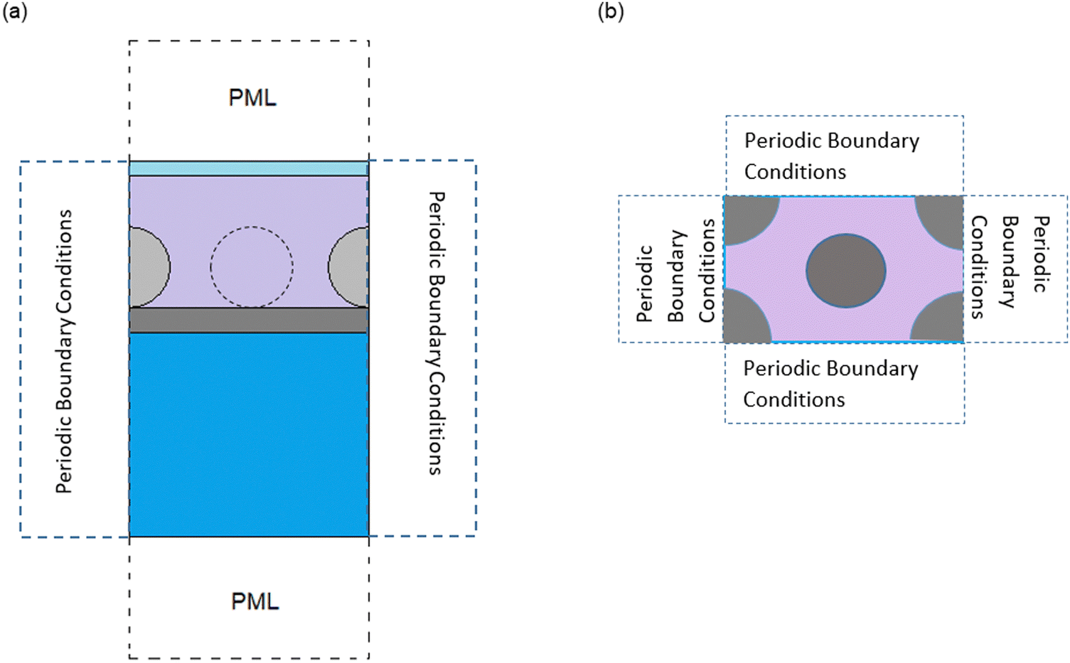 | ||
| Fig. 1 (a) Computational domain used in the electromagnetic modeling. (b) Rectangular unit cell used for representing the infinite NP periodic array. | ||
The spacing between NPs was kept constant at 50 nm and the NP diameter was changed from 40 nm to 70 nm. The total height of the computational cell is 349 nm, with following layer thickness: ITO = 12 nm, ZnO = 115 nm, SnO = 22 nm, Si = 200 nm. The optical constants used for the different materials were obtained from literature: ITO,24 ZnO,25 Si,26 SnO,27 Ag.28
The incident electromagnetic field (TM polarization) with power of 1 W was introduced from the top with the wave outlet at the bottom for the full-field solution. A perfectly matched layer (PML) with 150 nm thickness was implemented on the top and the bottom boundaries to ensure minimum artificial reflections from the boundaries. The built-in finer mesh element size (element sizes ranging from 4.3 to 59.3 nm) was selected giving a total of more than 68000 elements for the different nanoparticle setups. A Parallel Sparse direct Solver (MUMPS) was selected for solving the wave equation.
The outcome of each simulation is the electromagnetic field profile defined for all wavelengths in the range 400–750 nm. From this profile, the absorption A(λ) can be calculated by integrating the energy dissipation density within the appropriate volume according to:
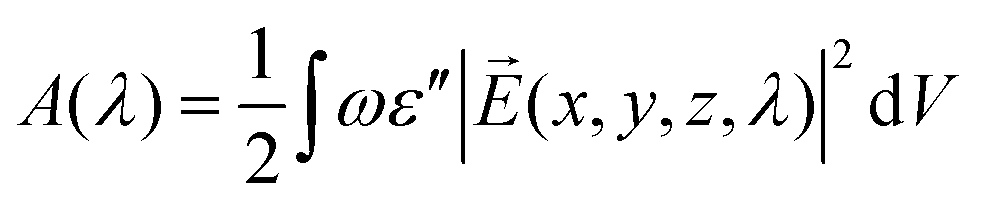 | (2) |
are the angular frequency and electric field strength of the electromagnetic field, respectively.
3. Results and discussion
Fig. 2(a)–(e) shows the SEM images of the surface of the Ag thin films on Si before growth of the SnO/ZnO heterojunctions. Well-separated Ag NPs were observed for the Ag@10, Ag@20 and Ag@40 samples. For longer Ag deposition times the separation of the NPs was no longer evident (i.e. a continuous layer was formed). The evolution of the Ag NP size and the covered surface area is shown in Fig. 2(f), where it is observed that the NP size increases from 37 nm up to 69 nm, and the surface area coverage decreases from 65% to 56% for Ag@10 to Ag40 to 100% for Ag@80 and Ag@160.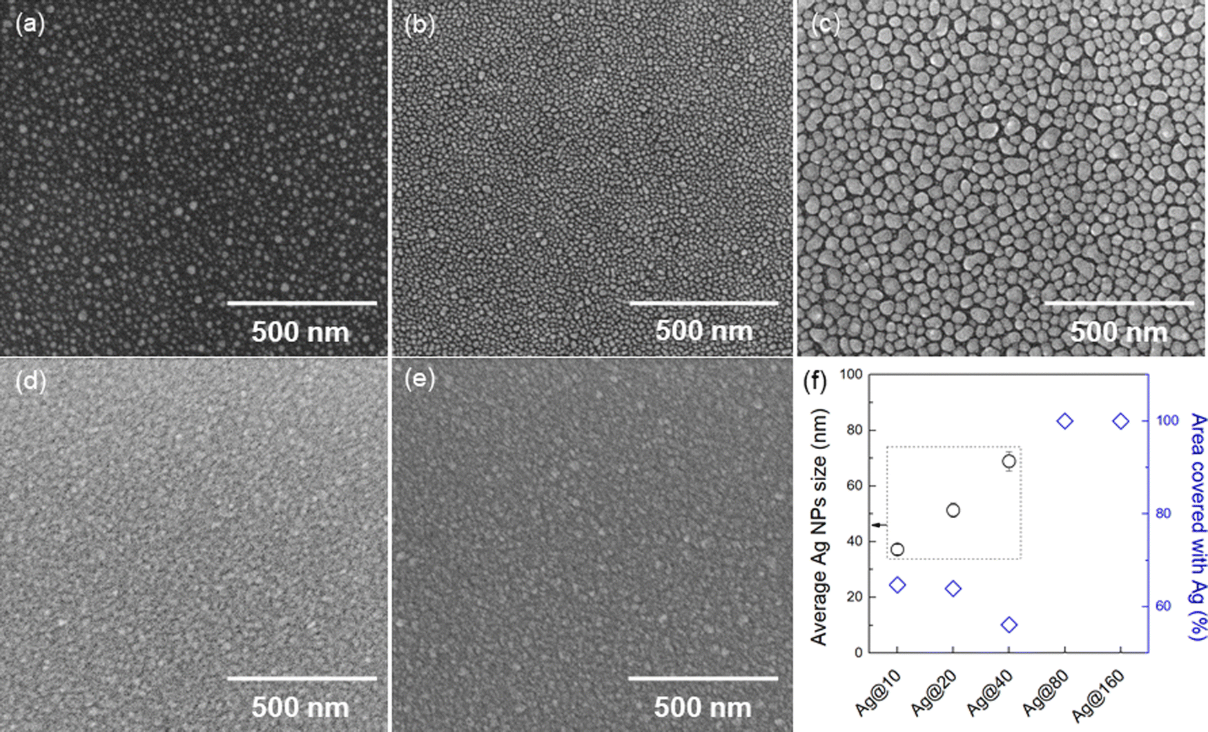 | ||
| Fig. 2 (a)–(e) Scanning electron microscopy images of the surface of the Ag thin films deposited on Si. The brightness and contrast of original images were adjusted to 40% and 20%, respectively. (f) Average Ag nanoparticles size and area of the Si substrate covered with Ag for the different samples. | ||
Fig. 3 depicts the UV-Vis absorption spectra of the Ag thin films deposited on glass. It can be concluded that the deposition time strongly influences the surface plasmon resonance (SPR) peak. The SPR wavelength shifts from 486 nm to 552 nm when the deposition time increases from 10 s up to 20 s. Moreover, with a further increase in the deposition time up to 40 seconds, the SPR peak remains practically at the same position, but the absorbance is higher. With a further increase of the Ag deposition time, it is possible to observe that the SPR peak disappears. This behavior confirms the creation of the Ag layer for deposition times 80 s and 160 s.
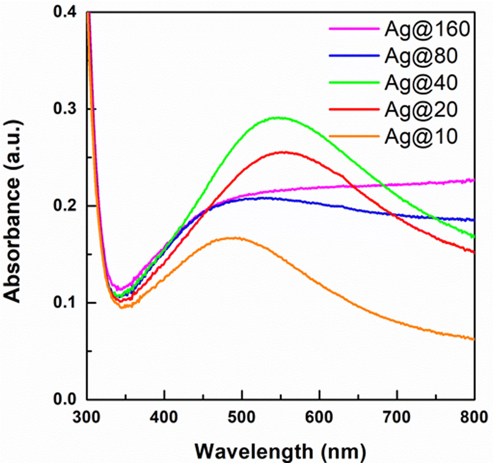 | ||
| Fig. 3 Optical absorption spectra of the different Ag thin films. | ||
The I–V characteristics of the Al/Si/SnO/Ag NPs/ZnO/ITO devices were measured in the dark and under 650 nm wavelength laser illumination for a fixed power density of 877 mW cm−2, as shown in Fig. 4(a) and (b), respectively. The asymmetrical behavior of the dark I–V curve indicates that the diode behavior of the device is due to the n–p–n heterojunction formed at the n-Si/p-SnO/n-ZnO interface.5Fig. 4(c) shows the rectifying ratio  for the different samples in the dark. It is observed that the RR decreases with the inclusion of the Ag NPs, suggesting that their inclusion degrades the SnO/ZnO heterojunction. However, and as shown in Fig. 4(b), the inclusion of the Ag NPs has a strong influence on the PV effect. Fig. 4(c) shows the short-circuit current (ISC) for the different samples and it is possible to observe that the sample Ag@40 exhibits the optimal PV performance due to the proximity of the surface plasmon resonance (SPR) wavelength to the wavelength of the laser illumination used and therefore higher light absorption. In addition, the surface area covered by Ag for Ag@40 is the smallest of all the samples with Ag NPs, thus allowing more light to reach the n-Si/p-SnO junction, which further enhances the PV effect.
 | ||
| Fig. 4 I–V curves (a) in the dark and (b) under 650 nm wavelength laser light illumination with a fixed power density of 877 mW cm−2 for the different samples. (c) Rectifying ratio and short-circuit current achieved for the different samples. | ||
The transient response characteristics of the Al/Si/SnO/AgNPs/ZnO/ITO devices, with different Ag deposition times, were investigated under zero bias and under the 650 nm laser illumination at a chopper frequency of 10 Hz. The I–t curves were measured at a fixed power density of 877 mW cm−2 and are shown in Fig. 5. The typical photocurrent dynamic response induced by the pyro-phototronic effect is observed for all samples, with repeatable features. In order to confirm that the spike current is due to the pyroelectric effect, the I–t curve was also measured under low frequencies for the Ag@20 sample, as shown in Fig. S1 (ESI†). It is possible to conclude that the response is due to the pyroelectric effect. It is possible to observe that, when compared to the sample without Ag NPs (Ag@0), the Ag NP layer not only enhances the PV effect, as already demonstrated in the I–V curves, but also the pyroelectric effect. Furthermore. The enhancement is independent of the morphology and optical response of the Ag thin layer.
 | ||
| Fig. 5 I–t curves for the different samples at a chopper frequency of 10 Hz for a fixed power density of 877 mW cm−2. | ||
Fig. 6(a) and (b) shows a schematic structure of the devices and energy band diagram of the Si/SnO/Ag NPs/ZnO heterojunction. The details of the band diagram for the Si/SnO/ZnO heterojunction are given in the previous work.17 When the laser light is turned on, the carriers are generated and separated due to the electric field associated to the PV effect (EPV) occurring at the p–n junction between p-SnO and n-Si. At the same time, the structure is heated up. This results in temperature gradient across the ZnO layer. An additional electric field is then generated due to the pyroelectric effect (Epyro), which increases the carrier separation at the junction and therefore a sharp current peak is observed from the combination of the PV and the pyroelectric effects.5 After the stabilization of the temperature across the structure, the gradient disappears. The Epyro is no longer effectively separating the carriers and so only an EPV is present which leads to a decrease in the observed current. In addition, when the light shines on the Ag NPs, the electromagnetic wave is coupled to the electron resonance. This results in oscillations of the free electrons and the emergence of an additional electric field. The plasmonic effect can extend up to 1 μm.29
 | ||
| Fig. 6 (a) Schematic representation of the pyro-phototronic effect in the Al/Si/SnO/Ag NPs/ZnO/ITO device and (b) energy band diagram for the Si/SnO/Ag NPs/ZnO heterojunction. (c) e-Field distribution around the central Ag NP, with a diameter of 70 nm, obtained by finite element simulation for wavelength of 650 nm. (d) Total absorbance in the full multilayer stack: without nanoparticle (black), and with NP different diameters: 70 nm (red), 50 nm (blue), 40 nm (green). (e) Power dissipated in ZnO layer (black) and Ag NP (red) as a function NP diameter for a wavelength of 650 nm. | ||
The EM interaction of the Ag NP array with light excitation was further elucidated through finite element simulations. The localized EM field and simulated absorbance of the Ag NP array with average size of 70 nm and average spacing of 50 nm are presented in Fig. 6(c) and (d), respectively. The simulated spectra, shown in Fig. 6(d), clearly exhibits an enhancement of the radiation absorption in the multilayer stack due to the localized surface plasmon resonance (LSPR) of the NPs. The plasmonic effect is also enhanced with an increase in the Ag NP diameter, with the plasmon peak shifting to longer wavelengths, in agreement with experimental observations. In addition, as shown in Fig. 6(c), the localized e-field distribution exhibits a stronger enhancement confined at the NP edges. Also, a large electric field intensity in the SnO layer originating from the LSPR effect from the Ag NPs, contributes to more efficient photocarrier separation and transport. The e-field enhancement also leads to a larger power dissipation in the ZnO layer and in the Ag NPs, as shown in Fig. 6(e). This can contribute to a larger heating of ZnO layer, thus explaining the increase in the pyro-current. Further, the generation and injection of hot carriers from the metal NP into the conduction band of the semiconductor layers can lead to an enhanced photovoltaic response.30 As the SnO layer has a thickness of 22 ± 3 nm, we can conclude that the electric field emerging from the nanoparticles reaches the p–n junction.
Overall, we conclude that the increase in the pyro- and photocurrent is caused by more effective charge-carrier separation at the junction due to the presence of an additional electric field from the LSPR effect. The possible formation of Ag/ZnO and Ag/SnO Schottky junctions could also have a significant impact on the pyro-phototronic effect.19 However, the dark current of the devices (Fig. 4(a)) is not suppressed with the formation of these Schottky barriers for the samples with Ag NPs confirming that this effect is less dominant in our samples. Moreover, while the Ag NPs in the sample Ag@40 absorbs more light when compared to samples Ag@10 and Ag@20 (see Fig. 3), they also cover a smaller surface area allowing more light to reach the n-Si/p-SnO junction, which enhances the PV effect in this case. In addition, larger NPs can absorb more energy from the neighborhood enhancing the gradient in the ZnO layer and further enhancing the pyroelectric effect. Therefore, synergistic coupling between the pyroelectric effect, the photovoltaic effect and the plasmonic effect is demonstrated.
As mentioned before, in the case of the Ag@80 and Ag@160 samples, a Ag layer is formed. In these cases, we can consider the sample as two devices in series: Al/Si/SnO/Ag and Ag/ZnO/ITO. In these cases, the PV effect is higher than the one observed in the Ag@0 sample because we have two back-to-back p–n junction barriers (i.e. n–p and p–n) of Si/SnO and SnO/ZnO, which blocks most of photo-generated carriers.5 We note that the pyroelectric effect of the Ag@80 and Ag@160 samples is reduced to a level closer to that in the Ag@0 sample because there is no plasmonic effect is present in any of these samples which could modify the pyroelectric effect.
The PD parameters such as responsivity (R), detectivity (D*) and sensitivity (S) were estimated with the following equations:10
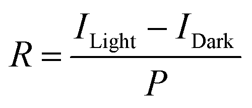 | (3) |
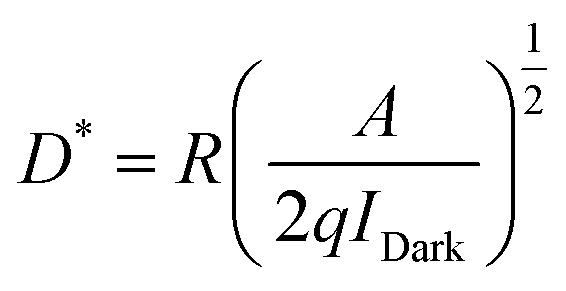 | (4) |
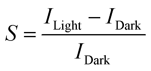 | (5) |
Fig. 7(a) shows the R, D* and S for the different samples. It is possible to observe that the sample Ag@40 reaches a maximum R of 72.3 mA W−1, with a D* of 18.8 × 10⁸ Jones and a S of 13.6 × 10⁴, as a consequence of the enhanced pyro-phototronic effect. As shown in Fig. 7(a), both R and D* values for samples with Ag NPs are higher than the samples without Ag NPs. In Table S1 (ESI†), it is shown the dark and photocurrent values are obtained through I–V and I–t measurements, respectively. It is possible to conclude that the dark current decrease with the inclusion of the Ag NPs and the photocurrent increases, suggesting that both effects contribute to the increase of R and D* values.
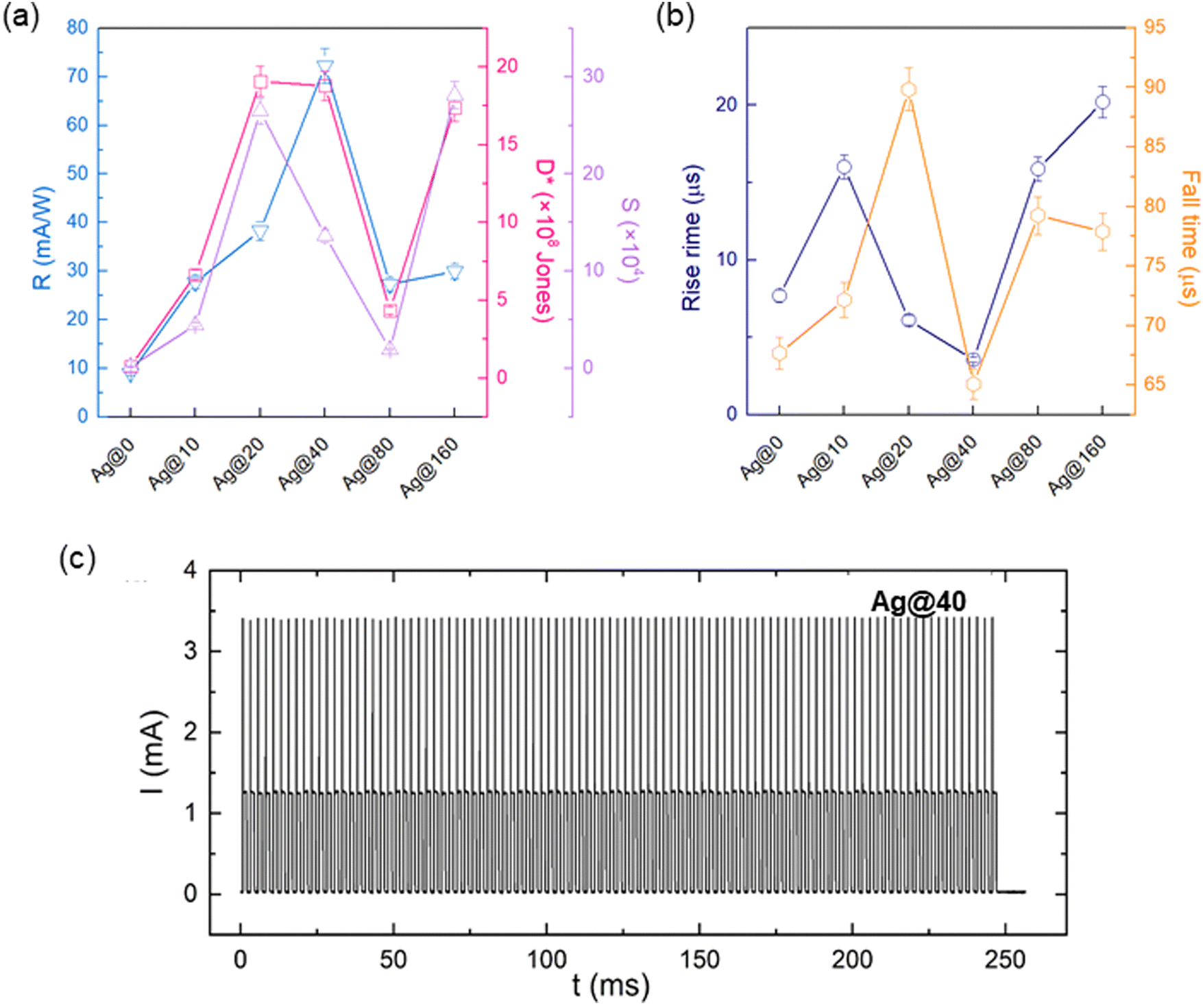 | ||
| Fig. 7 (a) Responsivity (R), detectivity (D*) and sensitivity (S) for the different samples. (b) Rise time (τr) and the fall time (τf) estimated for the different samples. (c) Stability of the transient response characteristics of the Ag@40 sample under zero bias and with 650 nm laser illumination and a laser power density of 887 mW cm−2. | ||
The rise time (τr) and the fall time (τf) were also evaluated for all the samples and are shown in Fig. 7(b). It is possible to observe that τr and τf have minimum values for the sample Ag@40 and are equal to 3.6 and 65.1 μs, respectively. The optimal PD parameters achieved in sample Ag@40 are a consequence of the plasmonic enhancement of the pyro-phototronic effect.
The stability of the transient response characteristics of the Ag@40 sample under zero bias and with 650 nm laser illumination is shown in Fig. 7(c). It is possible to observe that the PD exhibits a stable response up to 100 cycles.
In order to confirm the size of the Ag NPs in the Ag@40 sample, we performed TEM measurements. Fig. 8(a) is a CTEM image at low magnification, which shows in diffraction contrast imaging the morphology of our sample, which contains the following layers: ITO with an average thickness of 12 ± 3 nm, ZnO with an average thickness of 115 ± 5 nm, Ag nanoparticles with diameter around 60–70 nm and SnO layer with an average thickness of 22 ± 3 nm, and the Si substrate. Fig. 8(b) is a selected area electron diffraction image performed on the TEM image from Fig. 8(a), and it reveals the crystallinity of the sample. It contains a set of strong peaks, which can be assigned to the cubic Si structure of the substrate with space group Fd![[3 with combining macron]](https://www.rsc.org/images/entities/char_0033_0304.gif) m and a series of diffraction rings, which suggest the presence of some polycrystalline materials. From the measurements performed on the SAED pattern, we were able to index and assign a set of diffraction rings as follows: two of them were assigned to the tetragonal SnO structure with space group P4/nmm and a = b = 0.3849 nm, c = 0.4894 nm lattice constants, with Miller indices (101) and (002) and the other two were assigned to the wurtzite structure (hexagonal structure) of ZnO with space group P63mc and a = b = 0.3237 nm, c = 0.522 nm lattice constants, with Miller indices (100) and (002). Fig. 8(c) shows the high-angle annular dark-field scanning transmission electron microscopy (HAADF-STEM) image of the Si/SnO/Ag NPs/ZnO multilayered structure.
m and a series of diffraction rings, which suggest the presence of some polycrystalline materials. From the measurements performed on the SAED pattern, we were able to index and assign a set of diffraction rings as follows: two of them were assigned to the tetragonal SnO structure with space group P4/nmm and a = b = 0.3849 nm, c = 0.4894 nm lattice constants, with Miller indices (101) and (002) and the other two were assigned to the wurtzite structure (hexagonal structure) of ZnO with space group P63mc and a = b = 0.3237 nm, c = 0.522 nm lattice constants, with Miller indices (100) and (002). Fig. 8(c) shows the high-angle annular dark-field scanning transmission electron microscopy (HAADF-STEM) image of the Si/SnO/Ag NPs/ZnO multilayered structure.
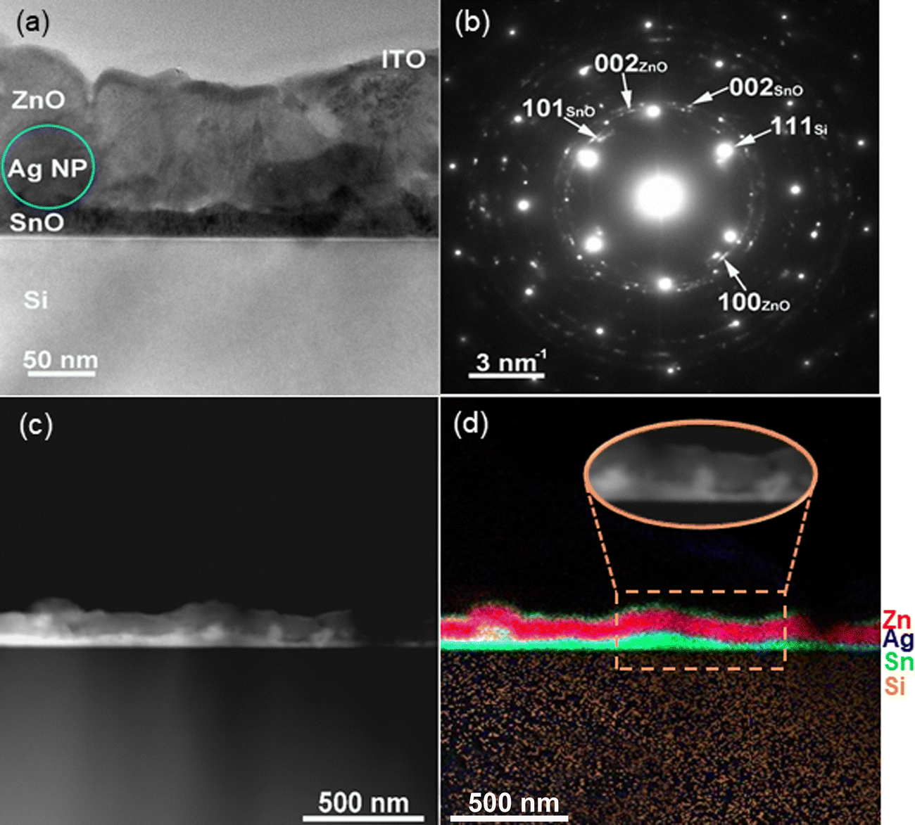 | ||
| Fig. 8 (a) Conventional transmission electron microscopy (CTEM) image at low magnification of the Si/SnO/Ag NPs/ZnO multilayered structure corresponding to sample Ag@40 and (b) electron diffraction diagram performed on an area from the TEM image shown in (a). (c) HAADF-STEM image of the Si/SnO/Ag NPs/ZnO multilayered structure. (d) Energy dispersive X-ray spectroscopy mapping of the high-angle annular dark-field scanning transmission electron microscopy shown in (c) obtained by overlapping the Si, Ag, Zn, Sn elemental maps. The inset shows a detail of the HAADF-STEM image showing the Ag NPs at the SnO/ZnO interface. | ||
In order to show the presence and the morphology of the Ag nanoparticles at the SnO/ZnO interface, we performed EDS mapping of the HAADF-STEM the results being present in Fig. 8(c). For every pixel of the HAADF image we acquired an EDS spectrum, thus obtaining an EDS map of each element present in the sample. Although, the EDS lines for Sn and Ag are quite close, we avoid them by choosing weaker lines for the Ag elemental map, i.e. the L line and M lines for the Sn elemental map. The EDS map shown in Fig. 8(d) was obtained by overlapping the Si, Sn, Ag, Zn maps and clearly point to a very sharp interface without any perceptible atomic interdiffusion between the layer, which is limited by the resolution of the EDS spectrometer. The Ag NPs have a spheroidal morphology with diameter around 60–70 nm, which is in good agreement with the SEM measurements. Inset into Fig. 8(d), is a magnified region of the HAADF-STEM image reveals the presence of Ag NPs at the SnO/ZnO interface.
Given that the pyro-phototronic effect is usually enhanced for lower power density,5,31 we measured the transient response characteristics for the best sample Ag@40 with a laser power density of 317 mW cm−2 as a function of the different chopper frequencies, in the range 10 up to 200 Hz. The measured I–t curves are shown in Fig. 9(a). It is possible to observe that the PD performance is almost independent of the chopper frequency. The PD parameters R, D* and S were found to be 210.2 mA W−1, 54.7 × 10⁸ Jones and 15.0 × 10⁴, respectively, while τr and τf are 2.3 and 51.3 μs, respectively for a chopper frequency of 10 Hz. This corresponds to an enhancement of 2.9 times in R and D*, and a decrease of the τr and τf of 36 and 21%, respectively, when compared to the same parameters measured at 877 mW cm−2.
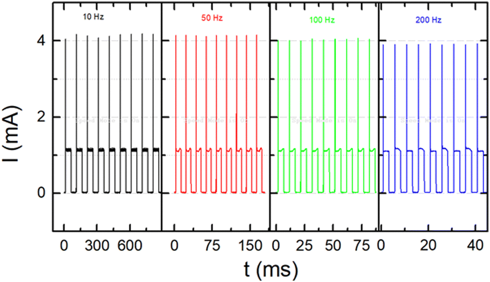 | ||
| Fig. 9 I–t curves for the Ag@40 device at different chopper frequencies and at a fixed power density of 317 mW cm−2. | ||
Table 1 shows a comparison of the R, D*, τr and τf of the self-powered PD obtained in this work with recent literature for other pyro-phototronic devices at different visible excitation wavelength. The present PD exhibits excellent responsivity, and the ultrafast fall and rise time make it promising for visible light detection. In addition, the lower detectivity observed in the present PDs can be attributed to an increase of the dark current observed in the samples with Ag NPs.
| Structure | Power density (mW cm−2) | Wavelength (nm) | R (mA W−1) | D* (Jones) | τ r (μs) | τ f (μs) | Ref. |
|---|---|---|---|---|---|---|---|
| Ag/Si/ZnO/ITO | 0.015 | 442 | 79.9 | 2.5 × 10¹⁰ | 600 | 500 | 15 |
| Ag/Si/ZnO/ITO | 0.34 | 633 | 17.9 | 6.4 × 10⁹ | 900 | 700 | 15 |
| Ag/Si/ZnO/ITO | 0.05 | 785 | 17.9 | 2.9 × 10⁹ | 2000 | 1800 | 15 |
| Al/Si/ZnO/PEDOT:PSS/ITO | — | 648 | 22.1 | — | — | — | 16 |
| Al/Si/SnOx/ZnO/ITO | 36.3 | 405 | 36.7 | 1.5 × 10¹¹ | 3 | 2 | 5 |
| Al/Si/SnOx/ZnO/ITO | 36.3 | 515 | 53.0 | 2.0 × 10¹¹ | 3 | 2 | 5 |
| Al/Si/SnOx/ZnO/ITO | 36.3 | 650 | 64.1 | 2.4 × 10¹¹ | 2 | 1 | 5 |
| Al/Si/SnO/ZnO/ITO | 36 | 405 | 93.0 | 2.4 × 10¹⁰ | 3.1 | 2.2 | 17 |
| Glass/FTO/ZnO/NiO/Ni | 0.08 | 400 | 3850 | 9.6 × 10¹³ | 24000 | 21200 | 32 |
| Al/Si/SnO/Ag NPs/ZnO/ITO | 317 | 650 | 210.2 | 5.47 × 10⁹ | 2.3 | 51.3 | This work |
4. Conclusion
Different to earlier works, Ag NPs were included to exploit the synergistic combination of the plasmonic effect and the pyro-phototronic effect to further enhance the visible response of a self-powered photodetector. To achieve that, a novel Al/Si/SnO/Ag NPs/ZnO/ITO device PD was developed. The influence of Ag NP morphology and optical properties on the photoresponse performance were explored after illumination with 650 nm laser light. Spheroidal Ag NPs with a diameter of ∼70 nm produced the optimum performance, i.e. to a strongly enhanced pyro-phototronic effect. The PD exhibited a responsivity, detectivity and sensitivity of 210.2 mA W−1, 5.47 × 10⁹ Jones and 15.0 × 10⁴, respectively, together with a rise and fall time of 2.3 and 51.3 μs, respectively. Through the plasmonic approach, in ZnO-based photodetectors it was possible to double the responsivity, while keeping an ultrafast rise and fall time response. The results are explained based on the coupling between the photovoltaic effect at the Si/SnO junction, and the plasmonic effect of the Ag NPs and the pyroelectric effect in ZnO that provided an extra electric field at the SnO/ZnO junction for charge separation. Moreover, the electromagnetic interaction of Ag NPs array with light excitation was elucidated through finite element simulations that confirm that the pyro- and photocurrent is caused by more effective charge-carrier separation at the junction due to the presence of an additional electric field from the LSPR effect. Therefore, the present work demonstrates that the combination of plasmonic Ag NPs with a ZnO pyroelectric film and a n-Si/p-SnO heterojunction is a promising materials combination for achieving highly-responsive and sensitive ultrafast photosensors.Data availability statement
The data that support the findings of this study are available from the corresponding author upon reasonable request.Author contributions
José P. B. Silva: conceptualization, methodology, validation, investigation, formal analysis, writing – original draft. Eliana M. F. Vieira: methodology, validation, investigation, formal analysis, writing – review & editing. Katarzyna Gwozdz: investigation, formal analysis, writing – review & editing. Nuno E. Silva: investigation. Adrian Kaim: investigation. Marian C. Istrate: investigation, writing – review & editing. Corneliu Ghica: resources, supervision, writing – review & editing. José H. Correia: resources, supervision, writing – review & editing. Mario Pereira: conceptualization, writing – review & editing. Luis Marques: investigation, formal analysis, conceptualization, writing – review & editing. Judith L. MacManus-Driscoll: conceptualization, writing – review & editing. Robert L. Z. Hoye: conceptualization, writing – review & editing. Maria J. M. Gomes: resources, supervision, writing – review & editing.Conflicts of interest
The authors declare no conflict of interest.Acknowledgements
This work was supported by: (i) the Portuguese Foundation for Science and Technology (FCT) in the framework of the Strategic Funding Contracts UIDB/04650/2020; (ii) CMEMS-UMinho Strategic Project UIDB/04436/2020 and UIDP/04436/2020 and (iii) the project M-ERA-NET3/0003/2021 - NanOx4EStor grant agreement No 958174 (https://doi.org/10.54499/M-ERA-NET3/0003/2021). J. P. B. S. also thanks FCT for the contract under the Institutional Call to Scientific Employment Stimulus – 2021 Call (CEECINST/00018/2021). The authors would like also to thank engineers Nuno Gomes and José Santos for technical support at the Thin Film Laboratory. K. G. acknowledges support from the National Science Centre in Poland Grant No. 2023/07/X/ST7/00073. M. C. I. and C. G. acknowledge the financial support by a grant of the Ministry of Research, Innovation and Digitization, CNCS/CCCDI – UEFISCDI, project number COFUND-M-ERANET-3-NanOx4Estor, within PNCDI III. J. L. M.-D. and R. L. Z. H. thank EPSRC CAM-IES grant EP/P007767/. R. L. Z. H. also acknowledges support from the Royal Academy of Engineering under the Research Fellowships scheme (No. RF\201718\1701). And J. L. M.-D. acknowledges support from the Royal Academy of Engineering Chair in Emerging Technologies scheme (No. CIET1819_24) and the ERC advanced grant, EU-H2020- ERC-ADG No. 882929, EROS.References
- D. You, C. Xu, W. Zhang, J. Zhao, F. Qin and Z. Shi, Nano Energy, 2019, 62, 310–318 CrossRef CAS.
- R. P. Rocha, M. J. Maciel, J. M. Gomes, J. P. Carmo and J. H. Correia, IEEE Sens. J., 2014, 14, 1343–1344 Search PubMed.
- B. Esteves, S. Pimenta, E. M. F. Vieira, J. R. Freitas, J. A. Rodrigues and J. H. Correia, Mater. Lett., 2021, 286, 129251 CrossRef CAS.
- S. Yang, M. Chen, X. Shen, Y. Yuan, Y. Liu, Q. Wang and D. Cao, Appl. Phys. Lett., 2021, 119, 121107 CrossRef CAS.
- J. P. B. Silva, E. M. F. Vieira, K. Gwozdz, A. Kaim, L. M. Goncalves, J. L. MacManus-Driscoll, R. L. Z. Hoye and M. Pereira, Nano Energy, 2021, 89, 106347 CrossRef CAS.
- J. P. B. Silva, K. Gwozdz, L. S. Marques, M. Pereira, M. J. M. Gomes, J. L. MacManus-Driscoll and R. L. Z. Hoye, Carbon Energy, 2022, 1–10, DOI:10.1002/cey2.297.
- S. Sahare, P. Ghoderao, M. K. Sharma, M. Solovan, R. Aepuru, M. Kumar, Y. Chan, M. Ziółek, S.-L. Lee and Z.-H. Lin, Nano Energy, 2023, 107, 108172 CrossRef CAS.
- V. Panwar, S. Nandi, M. Majumder and A. Misra, J. Mater. Chem. C, 2022, 10, 12487–12510 RSC.
- Z. Wang, R. Yu, C. Pan, Z. Li, J. Yang, F. Yi and Z. L. Wang, Nat. Commun., 2015, 6, 8401 CrossRef CAS PubMed.
- L. Chen, B. Wang, J. Dong, F. Gao, H. Zheng, M. He and X. Wang, Nano Energy, 2020, 78, 105260 CrossRef CAS.
- B. Yin, H. Zhang, Y. Qiu, Y. Luo, Y. Zhao and L. Hu, Nanoscale, 2017, 9, 17199–17206 RSC.
- J. Dong, Z. Wang, X. Wang and Z. L. Wang, Nano Today, 2019, 29, 100798 CrossRef CAS.
- B. Wang, Y. Zhu, J. Dong, J. Jiang, Q. Wang, S. Li and X. Wang, Nano Energy, 2020, 70, 104544 CrossRef CAS.
- X. Wang, Y. Dai, R. Liu, X. He, S. Li and Z. L. Wang, ACS Nano, 2017, 11, 8339–8345 CrossRef CAS PubMed.
- Y. Zhang, M. Hu and Z. Wang, Nano Energy, 2020, 71, 104630 CrossRef CAS.
- W. Peng, Z. Pan, F. Li, Y. Cai and Y. He, Nano Energy, 2020, 78, 105268 CrossRef CAS.
- E. M. F. Vieira, J. P. B. Silva, K. Gwozdz, A. Kaim, N. M. Gomes, A. Chahboun, M. J. M. Gomes and J. H. Correia, Small, 2023, 2300607 CrossRef CAS PubMed.
- Q. Li, J. Huang, J. Meng and Z. Li, Adv. Opt. Mater., 2022, 10, 2102468 CrossRef CAS.
- J. Huang, Q. Li, X. Lu, J. Meng and Z. Li, Adv. Mater. Interfaces, 2022, 9, 2200327 CrossRef CAS.
- J. Meng, Q. Li, J. Huang, C. Pan and Z. Li, Nano Today, 2022, 43, 101399 CrossRef CAS.
- Q. Li, J. Meng, J. Huang and Z. Li, Adv. Funct. Mater., 2022, 32, 2108903 CrossRef CAS.
- K. Kamakshi, J. P. B. Silva, K. C. Sekhar, G. Marslin, J. A. Moreira, O. Conde, A. Almeida, M. Pereira and M. J. M. Gomes, Appl. Phys. B: Lasers Opt., 2016, 122, 108 CrossRef.
- J. P. B. Silva, K. C. Sekhar, F. Cortés-Juan, R. F. Negrea, A. C. Kuncser, J. P. Connolly, C. Ghica and J. A. Moreira, Sol. Energy, 2018, 167, 18–23 CrossRef CAS.
- R. J. Moerland and J. P. Hoogenboom, Optica, 2016, 3, 112–117 CrossRef CAS.
- O. Aguilar, S. de Castro, M. P. F. Godoy and M. R. S. Dias, Opt. Mater. Express, 2019, 9, 3638–3648 CrossRef CAS.
- C. Schinke, P. C. Peest, J. Schmidt, R. Brendel, K. Bothe, M. R. Vogt, I. Kröger, S. Winter, A. Schirmacher, S. Lim, H. T. Nguyen and D. MacDonald, AIP Adv., 2015, 5, 67168 CrossRef.
- D. E. Guzmán-Caballero, M. A. Quevedo-López and R. Ramírez-Bon, J. Mater. Sci.: Mater. Electron., 2019, 30, 1366–1373 CrossRef.
- Y. Jiang, S. Pillai and M. Green, Sci. Rep., 2016, 6, 30605 CrossRef CAS PubMed.
- W. Jacak, E. Popko, A. Henrykowski, E. Zielony, K. Gwozdz, G. Luka, R. Pietruszka, B. Witkowski, L. Wachnicki, M. Godlewski, L.-B. Chang and M.-J. Jeng, Sol. Energy Mater. Sol. Cells, 2016, 147, 1–16 CrossRef CAS.
- S. Kunwar, S. Pandit, J. H. Jeong and J. Lee, Nano-Micro Lett., 2020, 12, 91 CrossRef CAS PubMed.
- Y. Wang, L. Zhu, Y. Feng, Z. Wang and Z. L. Wang, Adv. Funct. Mater., 2019, 29, 1807111 CrossRef.
- M. Patel, H.-S. Kim and J. Kim, Adv. Electron. Mater., 2015, 1, 1500232 CrossRef.
Footnotes |
| † Electronic supplementary information (ESI) available. See DOI: https://doi.org/10.1039/d3mh01725g |
| ‡ These authors contributed equally to this work. |
| This journal is © The Royal Society of Chemistry 2024 |