
 Open Access Article
 This Open Access Article is licensed under a
 Creative Commons Attribution 3.0 Unported Licence
Fully printed memristors made with MoS2 and graphene water-based inks†
Zixing
Peng
a,
Alessandro
Grillo
 a,
Aniello
Pelella
b,
Xuzhao
Liu
cd,
Matthew
Boyes
a,
Xiaoyu
Xiao
e,
Minghao
Zhao
a,
Jingjing
Wang
a,
Zhirun
Hu
e,
Antonio
Di Bartolomeo
b and
Cinzia
Casiraghi
*a
a,
Aniello
Pelella
b,
Xuzhao
Liu
cd,
Matthew
Boyes
a,
Xiaoyu
Xiao
e,
Minghao
Zhao
a,
Jingjing
Wang
a,
Zhirun
Hu
e,
Antonio
Di Bartolomeo
b and
Cinzia
Casiraghi
*a
aDepartment of Chemistry, University of Manchester, Oxford Road, Manchester, UK. E-mail: cinzia.casiraghi@manchester.ac.uk
bPhysics Department “E. R. Caianiello”, University of Salerno, via Giovanni Paolo II n. 132, Fisciano, 84084, Salerno, Italy
cDepartment of Materials, University of Manchester, Oxford Road, Manchester, UK
dPhoton Science Institute, University of Manchester, Oxford Road, Manchester, UK
eDepartment of Electrical and Electronics, University of Manchester, Oxford Road, Manchester, UK
First published on 26th December 2023
Abstract
2-Dimensional materials (2DMs) offer an attractive solution for the realization of high density and reliable memristors, compatible with printed and flexible electronics. In this work we fabricate a fully inkjet printed MoS2-based resistive switching memory, where graphene is used as top electrode and silver is used as bottom electrode. Memristic effects are observed only after annealing of each printed component. The printed memory on silicon shows low SET/RESET voltage, short switching times (less than 0.1 s) and resistance switching ratios of 103–105, comparable or superior to the performance obtained in devices with both printed silver electrodes on rigid substrates. The same device on Kapton shows resistance switching ratios of 102–103 and remains stable at least up to 2% of strain. The memristor resistance switching is attributed to the formation of Ag conductive filaments, which can be suppressed by integrating graphene grown by chemical vapour deposition (CVD) onto the silver electrode. Temperature-dependent electrical measurements starting from 200 K show that memristic behavior appears at a temperature of ∼300 K, confirming that an energy threshold is needed to form the conductive filament. This work shows that inkjet printing is a very powerful technique for the fabrication of 2DMs-based resistive switches onto rigid and flexible substrates.
New conceptsIn this work we demonstrate that water-based graphene and MoS2 inks, used as top electrode and switching layer, respectively, can be used to realize fully printed memristors with low SET/RESET voltage, short switching times (<0.1 s) and resistance switching ratios of 103–105, comparable or superior to the performance obtained in devices with both printed silver electrodes on rigid substrates. The same device printed on kapton shows resistance switching ratios of 102–103 and stable switching up to 2% of strain. Moreover, the devices show temperature dependent memristic behavior, which has never been observed in printed memristors of 2D materials. In addition, our work also provides insights on the filament formation mechanism. For example, we show that by integrating CVD graphene onto the silver electrode enables to completely remove the memristic effect. This work shows that inkjet printing is a very powerful technique for the fabrication of 2DMs-based memristic devices onto rigid and flexible substrates. |
1. Introduction
The development of memristic devices capable of storing multiple states of information is required for many applications, ranging from data computation to neuromorphic circuits and adaptive systems.1–4 Research has mostly focused on the improvement of the device performance parameters, such as fast switching speeds, low energy consumption, and high endurance. However, it is also of crucial importance to show integration of such devices onto flexible substrates, enabled by the use of low-cost and mass scalable technologies such as inkjet printing.2D materials are very attractive for the fabrication of printed memristors as they can be easily processed into inkjet printable formulations and used to fabricate the full device.5–13 However, very few works have reported fully printed 2DMs-based memristors: most of the literature is based on the use of non-scalable deposition methods such as spin coating or drop casting. In particular, only 3 works have reported printed memristors made of 2DMs,14–16 while few works have also reported printed devices made with other types of nanomaterials17–28 (see ESI,† Tables SI and SII). In literature, fully printed 2DMs-based devices have been made by using silver to print both the bottom and top electrode. The use of silver is considered mandatory for the fabrication of printed 2DMs resistive switches based on electrochemical metallization (ECM), as it enables the formation of conductive filaments between the electrodes.14 However, there is no comprehensive research on how the filament is formed and propagates in a randomly assembled network of nanosheets, as produced by printing techniques, hence leading to poor device reproducibility and limited endurance. In addition, defects in MoS2 nanosheets have been also attributed to memristic effects,29,30 hence the fundamentals of the switching mechanism in printed devices is not completely understood.
Herein, using water-based 2DMs and silver inks, we fabricated MoS2-based ECM resistive switches by inkjet printing, using silver as bottom electrode and graphene (Gr) as top electrode (heterostructure: Ag/MoS2/Gr). The ability to replace the printed silver with graphene enables to achieve better mechanical flexibility, without degrading the performance of the device: under optimized conditions, the fully printed Ag/MoS2/Gr memristors offer performance comparable to those obtained in printed devices with silver as electrodes and with other nanomaterials, such as TiO2 and ZrO2, on rigid substrates.19,22,24 The same device printed on Kapton shows a stable memristic behavior up to at least 2% of strain. Finally, we show that the memristic effect can be hindered by the integration of CVD Gr onto the silver electrode. Remarkably, hysteresis is also strongly reduced when CVD Gr is integrated in a Gr/MoS2/Gr heterostructure, showing that CVD Gr not only acts as a barrier for the ions migration, but also enables to improve the interface between the electrode and the dielectric layer, hence enhancing the reliability and reproducibility of the device.
2. Results and discussion
Fig. 1a shows the schematic of the printed Ag/MoS2/Gr memristors. The inset displays an optical picture of 6 memristors printed onto silicon (SiO2/Si), using the same ink and printing conditions (see Methods). The inset in Fig. 1b shows a higher magnification optical image of one of the memristors, showing that the film edges are well defined – no visible blemishes or breakages of the films are observed, confirming good printability of the inks on the SiO2/Si substrate. To note that the thickness of the silver film is found to be also important in the optimization of the device fabrication: if the silver film is too thick, cracks appear in the MoS2 film (Fig. S1, ESI†), which is printed on top of it, leading to devices with no resistive switching (RS) behavior.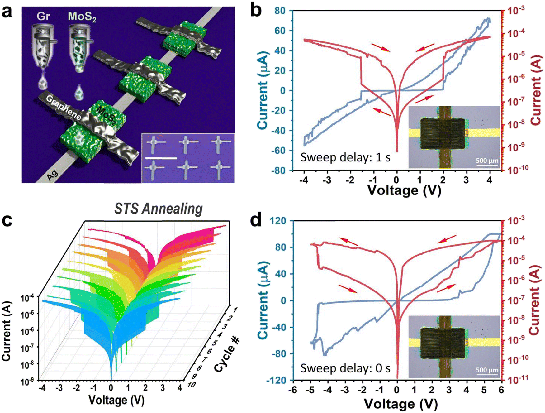 | ||
| Fig. 1 Electrical properties of fully printed Ag/MoS2/Gr memristors. (a) Schematic of fully printed Ag/MoS2/Gr memristors. Inset: Optical picture of 6 printed devices on silicon, scale bar: 5 mm. (b) Representative I–V curve of the Ag/MoS2/Gr device; inset: optical image at high magnification of the Ag/MoS2/Gr memristor. (c) I–V curves taken over 10 cycles of the device made with STS. (d) Representative I–V curve of a non-volatile Ag/MoS2/Gr memory obtained by applying a continuous sweep voltage to the device shown in panel b. | ||
All devices were made with a step-by-step (STS) annealing, where each film of the heterostructure was annealed after printing (see Experimental section for more details). Fig. 1b shows the electrical characteristics of the device obtained at a current compliance of 10−4 A: a clear threshold-type volatile RS behavior is observed, i.e. the memristor abruptly switches from a high resistance state (HRS) to a low resistance state (LRS) beyond a threshold voltage, associated to the “SET process”, and then shows resistance recovery when the bias is removed, no matter the polarity of the sweep voltages. Fig. 1c shows the I–V curves measured over 10 cycles. However, when we apply a continuous sweep voltage, the switching characteristic turns into a non-volatile behavior, as shown in Fig. 1d. In this case, after setting the memristor in LRS with a switching voltage of ∼5 V, a voltage bias with opposite polarity is required to make a RESET process, i.e. to bring the memristor to HRS.
As the memristic effect is expected to be caused by migrations of silver ions and formation of conductive filaments, the overlapped area between the silver electrode, the dielectric layer and the top electrode is expected to affect the performance of the device. Hence, the overlapped area has been changed by varying the width of the Ag film from 0.1 mm to 0.5 mm. The optical images of the devices are shown in Fig. S2 (ESI†). Fig. S3 (ESI†) shows that the Ag/MoS2/Gr memristors achieve higher RS ratio with a relatively small active area. This seems to be counterintuitive, however one should consider that the uniformity of the silver film is expected to decrease by increasing the printed area, for example some pin-holes are visible on the widest silver films (Fig. S2, ESI†). Overall, the device with 0.2 mm width Ag bottom electrode shows the best performance, amongst all devices investigated (Fig. S4, ESI†).
We also compared two different annealing processes: STS and final-step (FS) annealing, in which the device was annealed only once, and after printing of all components. Fig. S5a (ESI†) shows the I–V curves measured over 10 cycles for a Ag/MoS2/Gr device made with FS annealing: only hysteresis is observed. Fig. S5b (ESI†) shows the memristor performance, reported as the RS ratio, defined as the resistance ratio between the current measured at the LRS and HRS (ILRS/IHRS) for all the Ag/MoS2/Gr memristors, fabricated with different geometries (see ESI,† Table SIII for full details on the devices geometry) and divided by type of annealing. Note that in Fig. S5b (ESI†) we normalized the Ag/MoS2/Gr memristors by the active area. This figure shows that STS annealed memristors are more likely to achieve RS ratio above 102. A maximum RS of 105–106 can be achieved, if the device is properly optimized. In contrast, the memristic effect is hardly visible when FS annealing is used, with RS ratio of 102 achieved only for a few devices.
In order to further investigate the effect of annealing on the memristic behavior, we performed profilometry, cross-sectional scanning electron microscopy (SEM), X-ray diffraction (XRD) and X-ray photoelectron spectroscopy (XPS). However, we did not observe any strong change in the elemental composition and structure of the films, before and after annealing (Section S4, ESI†), in the limit of the experimental resolution. Since pyrene melting temperature is ∼400 °C, while glycol propylene, Triton-X and Xanthan gum melt at 200–270 °C, annealing at 150 °C is expected to remove mainly residual water from the film. Previous studies on printed capacitors31 have shown that STS annealing allows to better remove residual water from the film, hence enabling to measure the dielectric constant of printed h-BN films. Based on these observations, we can conclude that the removal of water molecules somehow affects the memristic behavior, i.e. STS annealing is needed to see memristic effects in our device because this process is more efficient than FS annealing at removing the residual solvent from the printed film. Furthermore, it is likely that the printed film may have also a slightly different morphology when subjected to the different types of annealing but this cannot be resolved with traditional characterization techniques. It is clear that both the morphology and the presence of additional molecules trapped in the film are crucial to obtain devices with memristic effects, i.e. the structure and composition of the film affect the formation of the silver filament. Therefore, we predict that by finely controlling the morphology, porosity and composition of the printed dielectric film (e.g. amount of residual solvent), the RS ratio could be even further improved.
Fig. 2a shows a pulsed voltage test on the optimized Ag/MoS2/Gr memristor. A voltage of 4 V was applied with 1 second pulse (ON/OFF time). After applying the pulsed voltage for a total of 30 s, the device reaches the SET condition, by switching on in just 0.1 s (Fig. S10, ESI†). The relatively rapid RS capability enables fabrication of non-volatile Ag/MoS2/Gr memristors. Fig. 2b summarizes the SET and RESET voltages of 50 memristors. It can be seen that all devices are working, but due to the non-uniformity of the inkjet printing devices, the SET and RESET voltages are distributed in a small range, with the most frequent SET voltage seen at about +2 V, while the RESET voltage is slightly smaller, at around −1 V. To note that a voltage switching range from ±1.4 to ±5![[thin space (1/6-em)]](https://www.rsc.org/images/entities/char_2009.gif) V has been observed in devices that have been proposed for integration of 2D based memristor in CMOS technology.32
V has been observed in devices that have been proposed for integration of 2D based memristor in CMOS technology.32
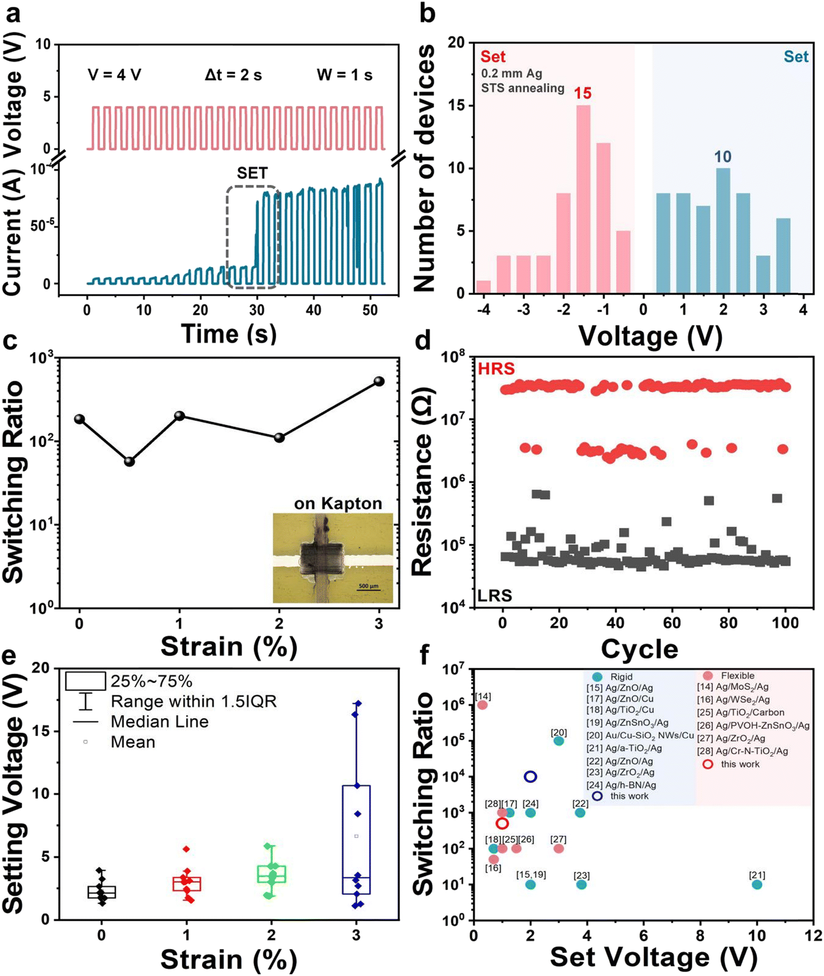 | ||
| Fig. 2 Switching behavior of the Ag/MoS2/Gr memristors. (a) The current response from input voltage pulses generated by the Ag/MoS2/Gr device, made with STS annealing. (b) Statistical distributions of VSET over 50 devices. (c) Resistive switching characteristics of the Ag/MoS2/Gr memristors printed on Kapton. Inset: Optical image of a printed devices on Kapton. (d) Cycle endurance test of a single Ag/MoS2/Gr on Kapton. (e) Switching voltage measured on 10 Ag/MoS2/Gr devices printed on Kapton under bending at different strain. (f) Benchmarking of the fully printed Ag/MoS2/Gr memristor compared to state-of-the-art printed memristors fabricated on rigid and flexible substrates. | ||
We have also conducted up to 100 cycles of rapid testing and examined the stability of the optimized memristor in both HRS and LRS, finding that the device can keep switching for over 100 cycles and remains stable in both HRS and LRS for at least 104 seconds with negligible degradation. The estimated lifetime of the memristors in the LRS state is about 1000 hours (Fig. S11, ESI†). Fig. S12 (ESI†) shows that the switching speed of the memristors increases when the voltage applied between the two electrodes is increased, so as the ON/OFF ratio of the device. The higher voltage is expected to speed up the migration of Ag ions in the MoS2 dielectric layer and to promote the rapid switching of the memristors. The memristor can set in few seconds even when narrow pulses voltage (Δt = 0.5 s and 0.6 s) are applied. In particular, with a set voltage of 3V, the memristor can switch for over 100 cycles, as shown in Fig. S13 (ESI†).
Since our devices are fabricated by inkjet printing, they can be easily integrated onto flexible substrates. The inset in Fig. 2c shows the optical image of a fully-printed Ag/MoS2/Gr memristor printed on Kapton. Fig. S14 (ESI†) shows its I–V characteristics over 10 cycles: each cycle shows stable memristic behaviour. Fig. 2c shows the results of a bending test: the RS ratio remains around 102 up to strain of 3%; Fig. 2d and Fig. S15 (ESI†) shows that the RS ratio of the pristine and strained (under 1% and 2% strain) Ag/MoS2/Gr memristors on Kapton remains between 102–103 for over 100 cycles. Fig. S16 (ESI†) shows the LRS and HRS and the I–V characteristics of a Ag/MoS2/Gr memristor that has been bent for 500 times with a bending radius of 2.5 mm (corresponding to 1% strain) and 1.25 mm (corresponding to 2% strain). Both devices show similar switching characteristics of the pristine (i.e. unbent) device printed on Kapton. The bending endurance is comparable to most of the reported values for printed memristors (ESI,† Table SII(b)). This demonstrates the suitability of the devices for flexible and printable electronics. The switching voltage of the device under bending conditions has also been reported in Fig. 2e, including statistical analysis (see full set of data in ESI,† Table SV), showing good reproducibility of the performance parameters for strain up to 2%. Finally, Fig. 2f compares the RS and the set voltage of our printed memristors with fully printed memristors based on various nanomaterials from the state of art (see ESI,† Tables SI and SII). When printed on rigid substrate, our devices show the highest RS for a SET voltage below 2 V; on flexible substrate, our devices show performance comparable to most of the printed memristors reported in literature made with silver electrodes.
In silver-based ECM memristors, the RS mechanism is explained by the Ag ions migration in the MoS2 dielectric layer. When a bias was applied on the device, the Ag atoms in the bottom Ag electrode are oxidized to Ag+ ions by the Joule effect of the electric field. Afterwards, the Ag+ ions are driven to the top graphene electrode by the applied electric field, leading to the re-distribution and accumulation of the space charge. When reaching the graphene electrode, the Ag cations are gradually reduced to Ag atoms, leading to the Ag filament formation, which facilitates the switch from the HRS to LRS. In contrast, with the applied reverse bias on the device, the Ag atoms of the conductive filament are oxidized to the Ag+, which then migrate to the Ag electrode under the electric field. This leads to the dissolution of the conductive filament, causing the resistance to switch from LRS to HRS. To verify this mechanism, we printed a control device where Gr was used for both electrodes, Fig. S17 (ESI†): no resistance switching behavior is observed, as expected – just a small hysteresis is seen, similar to the one observed in the FS annealed Ag/MoS2/Gr device (Fig. S5a, ESI†).
Furthermore, the ECM-based RS mechanism can be easily checked by fitting the I–V curve of the Ag/MoS2/Gr memristor, as shown in Fig. 3a: in the HRS phase, the slope is 1.20 between 0 V to 1 V, showing a linear Ohmic conduction (J ∝ V, where J is the current density); the slope increases for V > 1 and it is well fitted with the Childs square at high bias (i.e. J ∝ V2), indicating that the charge transport in the HRS fits well with the space charge limited current (SCLC) model,33 in agreement with other works.34 The slope of the I–V curve of the LRS is 1.22, close to 1, indicating that charge transport conforms to the Ohmic law, in agreement with the filament formation mechanism. Hence, alternative RS models35 where contribution on the memristic effect was explained by the presence of a Schottky barrier between the MoS2 flakes and the electrode, with the MoS2 flakes acting as electron trapping centers, are not valid for our devices.
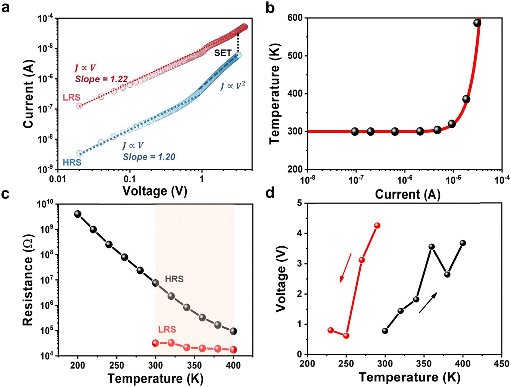 | ||
| Fig. 3 Resistance switching mechanism of the Ag/MoS2/Gr memristor. (a) The positive part of the I–V curve in double logarithmic coordinates shows Ohmic behaviour in LRS and SCLC behaviour in HRS. (b) Temperature of the conductive filaments as a function of current, calculated using eqn (1). (c) LRS and HRS resistance of the Ag/MoS2/Gr memristors as a function of the temperature in the 200–400 K range. (d) Setting voltage as a function of the temperature in the 200–400 K range recorded by increasing (black line) and decreasing temperature (red line). | ||
Finally, following the model proposed in ref. 23, we also extracted the temperature of the conductive filaments using the following equation:36
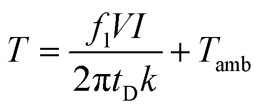 | (1) |
Moreover, we performed electrical measurements at different temperatures, starting from 200 K and increasing the temperature to 400 K with 20 K steps, which have never been reported for printed memristors. Fig. S19 (ESI†), Fig. 3c and d show that memristic behaviour is observed only when the temperature reaches 300 K. Furthermore, Fig. 3c shows that in the HRS, the resistance of the device decreases with the temperature, as expected for a semiconductor.38 In the LRS, the resistance remains around 104 Ω, independent of the temperature, as expected for a metal. Moreover, Fig. 3d shows that the setting voltage changes with the temperature. For both the measurements recorded by increasing temperature and decreasing temperature, the setting voltage increases with the temperature. Normally, higher temperature should help silver ions migration, so this observation may indicate a change in the micro-structure of the printed MoS2 film for increasing temperature, which may hinder the ions migration. Alternatively, this may indicate the presence of another memristic mechanism, in addition to the silver filament, for example related to defects in the MoS2 film. On the other hand, printed memristors show setting voltage in the range 1–4 V (Fig. 2b), so this variation may simply be within the device-to-device fluctuation range.
To further investigate the origin of the memristic effect observed in the Ag/MoS2/Gr device, we used CVD graphene as impermeable barrier,39–43 by integrating this material (see Experimental and Section S10, ESI† for details) onto the silver electrode. CVD graphene is expected to prevent silver ions migration from the electrode to the dielectric. Fig. 4a–d show that although the transfer of graphene is not perfect (e.g. some folding and wrinkles are observed, possibly due to the rough silver surface), still it is possible to transfer graphene on a relatively large area with good coverage.
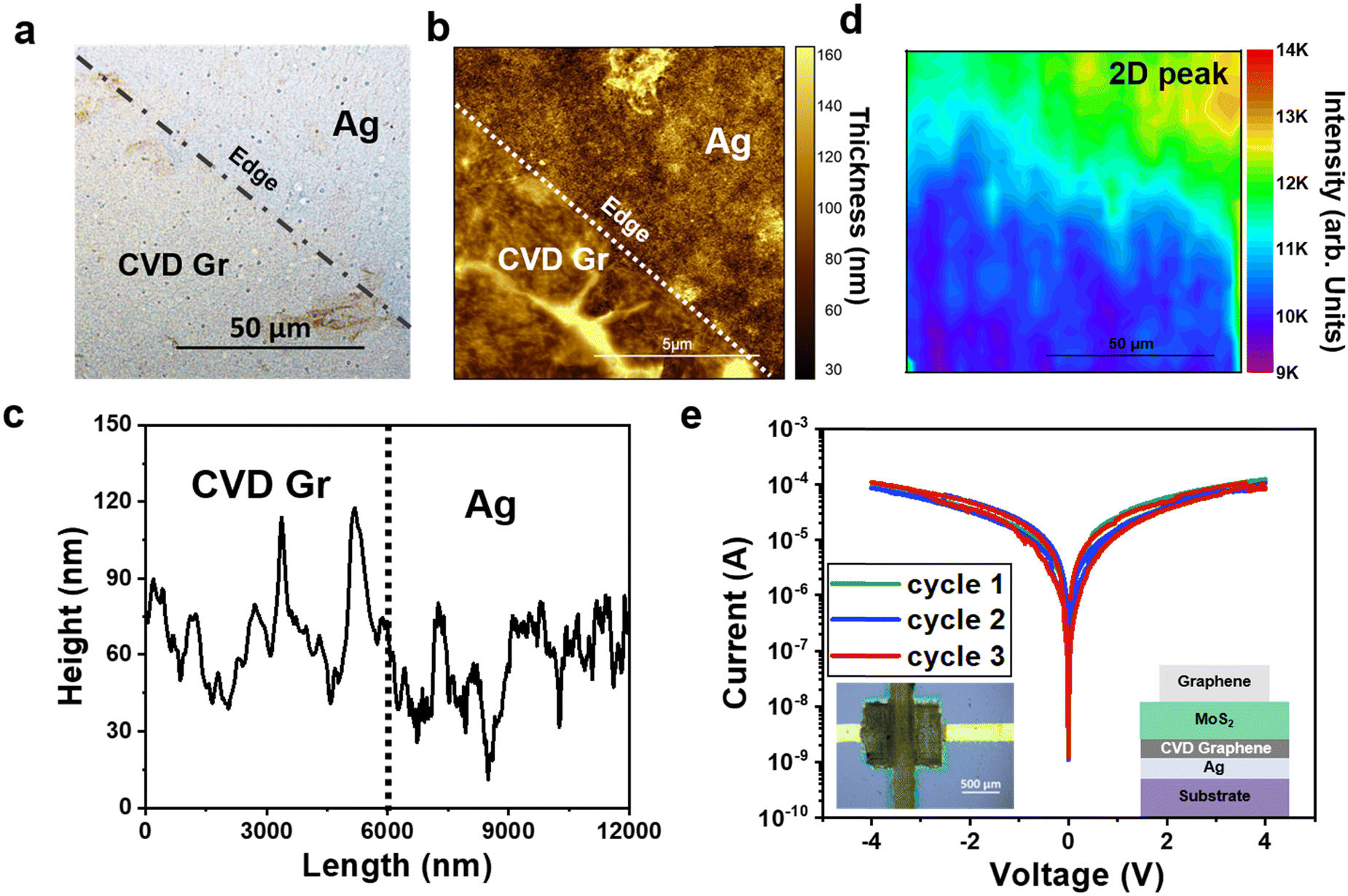 | ||
| Fig. 4 Ag/MoS2/Gr memristors with integration of CVD graphene. (a) Optical image, (b) and (c) AFM image and (d) Raman mapping of the 2D peak intensity of CVD graphene transferred onto the printed Ag electrode. (e) I–V curves of the Ag/CVD Gr/MoS2/Gr device; inset: optical image of the device. | ||
Fig. 4e shows the I–V characteristics of the Ag/CVD Gr/MoS2/Gr device: no memristic behaviour is observed, confirming that the silver ions migration from the bottom Ag electrode to the top graphene electrode is strongly reduced by the presence of the CVD graphene. Remarkably, the hysteresis window is strongly reduced as compared with that observed in the Gr/MoS2/Gr device, showing that CVD graphene enables to improve the quality of the interface, possibly by reducing the number of defects/trap states. Hysteresis is an unwanted effect as it makes the I–V characteristic not reproducible and can produce artefacts if measurements are taken too quickly,44 so it is of crucial importance to understand the origin of hysteresis and find ways to minimize it. Our results show that the integration of CVD graphene onto printed electrodes is a simple solution to minimize the hysteresis, hence improving the reliability and reproducibility of the devices.
To note that we also investigated transfer of CVD graphene in the dielectric layer and at the interface between the dielectric layer and the top electrode (Ag/MoS2/CVD Gr/MoS2/Gr) and Ag/MoS2/CVD Gr/Gr, respectively. See Experimental and Section S10 (ESI†) for more details. In the first configuration, none of the devices have shown a clear memristic effect, confirming the ability of CVD graphene to block the filament formation. In the second case, some devices still show memory effects, see full data in ESI,† Table SVII, possibly due to the increased difficulty in device fabrication, leading to poor device reproducibility.
3. Conclusions
In summary, we have investigated the memristic behaviour of fully inkjet printed heterostructures made by using water based 2D material inks and silver ink for the bottom electrode. Under careful optimization, we demonstrated fully printed Ag/MoS2/Gr memristors exhibiting improved performance as compared to fully printed memristors on rigid substrate made of other nanomaterials using silver electrodes.The memristic effect is originated by the migration of silver ions to form conductive filaments and can be completely blocked by transferring CVD graphene onto the silver electrode. We finally demonstrate a fully printed Ag/MoS2/Gr memristors on Kapton showing reliable and stable signal up to 2% strain, hence revealing the potential of 2DMs printable inks for the development of the next generation of flexible memristors.
4. Experimental
Materials
Bulk graphite flakes (99.5% grade) were purchased from Graphexel Ltd. Molybdenum disulfide powder (<2 μm, 99%) and pyrene-1-sulfonic acid sodium (PS1) were purchased from Sigma Aldrich (>97%). De-ionised water was prepared by a Millipore Simplicity 185 water purification system with the resistivity of ∼18.2 MΩ cm (at RT). The silver ink was purchased from Sigma Aldrich (1.45 g mL−1 ± 0.05 g mL−1, 30–35 wt% in triethylene glycol monomethyl ether).Silver conductive paste was sourced from Sigma Aldrich. Triton X-100 and Xanthan gum were purchased from Sigma-Aldrich, UK. Silicon wafers with an oxide layer thickness of ∼300 nm were purchased from IDB Technologies Ltd and cleaned by sonication, using a Sonorex RK 100 bath sonicator, in acetone and Isopropyl Alcohol (IPA) at 35 kHz for 15 minutes, each respectively prior to use. Monolayer graphene on Cu grown by CVD was purchased from Graphenea. Anisole was purchased from Honeywell (99%). Poly(methyl methacrylate) (PMMA) was purchased from Sigma Aldrich (average Mw = 350000, measured by GPC). 10 μL Dimatix cartridges were purchased from Printed Electronics Ltd.
Preparation and characterization of graphene and MoS2 inks
The ink preparation is described in ref. 5. In details, the dispersion was sonicated at 300 W using a Hilsonic bath sonicator for 120 hours. Flakes of appropriate lateral size were collected via differential centrifugation to reduce the chance of nozzle blockages. The liquid obtained was centrifuged using a Sigma 1–14k refrigerated centrifuge at 3500 rpm (903 g) for 20 minutes before collecting the supernatant. The collected supernatant was then centrifuged at 15000 rpm (16600 g) for 1 hour and the precipitate re-dispersed in the printing solvent. The solvent consists of less than 1:10 propylene glycol:water by mass, ≥0.06 mg mL−1 Triton X-100 and ≥0.1 mg mL−1 Xantan gum. The concentration of 2D material was determined by UV-Vis spectroscopy. The dispersion was diluted to reach a concentration of 2 mg mL−1, as measured by absorption spectroscopy with a PerkinElmer l-900 UV-vis-NIR spectrophotometer. Absorption coefficients of 2460 L g−1 m−1 (at 660 nm) and 3400 L g−1 m−1 (at 670 nm)45 were used for graphene and MoS2, respectively. No aggregation is observed when the material is transferred in the cartridge or during printing.
Transfer of CVD graphene
Commercial CVD graphene was transferred to SiO2/Si substrate by PMMA-based transfer method. PMMA powder was dissolved in anisole at 80 °C to form a 9 wt% PMMA solution. The PMMA solution was spin coat onto CVD graphene at 2500 rpm for 60 s, then the sample was heated at 170 °C for 5 min. The sample was then placed in 0.5 mol% (NH4)2S2O8, (6–12 h) to etch the copper substrate. The sample is then cleaned with DI water to remove extra (NH4)2S2O8 and then transferred to the SiO2/Si substrate. The PMMA film on the surface was dissolved by soaked into acetone and at last the sample is dried by N2 airflow.Device fabrication
The SiO2/Si and Kapton substrates are cleaned by acetone and IPA and then treated with Ar plasma for 15 s to improve printability. A Fujifilm Dimatix DMP 2800 printer was used to fabricate the devices. Printing was performed at a platen temperature of 45 °C and drop spacing of 35 μm.5 The graphene film was printed with 60 printing passes, giving a film thickness of ∼200 nm on silicon (Fig. S6, ESI†). The silver ink was printed with one pass (corresponding to a film thickness of ∼100 nm), as more passes result in cracks formation of the MoS2 film.Two post-processing approaches were investigated: (i) STS annealing, where annealing is performed after printing each film of the heterostructure. The Ag and 2D material-based films were annealed at 150 °C for 30 min and 90 min, respectively, in vacuum. Note that after annealing, the printability on the silicon is not good enough, so the sample is subjected to a 15 s Ar plasma treatment before the next material is printed. This treatment does not affect the structure of the printed MoS2 film as shown by UV-Vis and Raman spectroscopy (ESI,† Section S10). (ii) FS annealing, where the device is first fully printed and then annealed once at 150 °C for 180 minutes under vacuum. 50 devices were made for each post-processing conditions.
In the case of the devices containing CVD Gr, three types of devices were investigated:
(i) Ag/CVD Gr/MoS2/Gr devices, where the CVD graphene is transferred on top of the Ag electrode, hence acting as interface between the silver and the MoS2 dielectric layer;
(ii) Ag/MoS2/CVD Gr/MoS2/Gr devices, where the CVD graphene is integrated in the MoS2 dielectric layer, after 20 passes of the MoS2 printed on the Ag, the CVD graphene is transferred, then 60 passes more MoS2 is printed, hence the CVD graphene acting as barrier inside the dielectric.
(iii) Ag/MoS2/CVD Gr/Gr devices, where the CVD graphene is transferred on top of the MoS2 dielectric layer, hence acting as interface between the dielectric and top electrode.
Ar plasma treatment for 60 s was performed after finishing the whole printing process, in order to remove excess CVD graphene.
All devices containing CVD graphene were made with STS annealing before CVD graphene was transferred onto the heterostructure.
Raman spectroscopy
A Renishaw Invia Raman spectrometer, equipped with a laser with excitation wavelength of 514.5 nm and 2 mW laser power, a 100× NA, 0.85 objective lens and a 2400 grooves mm−1 grating was used. The Raman spectra were collected on 10 different spots for each sample to check for sample uniformity.UV-Vis absorption spectroscopy
A PerkinElmer l-900 UV-vis-NIR spectrophotometer was used to measure the UV-vis spectra of the MoS2 films drop-casted on quartz glass.XRD Spectroscopy
XRD spectra were acquired using a Bruker D8 Discover Autochanger, equipped with CuKa source. The step size and dwell time was set to be 0.02 degree and 2 s, respectively.X-ray Photoelectron Spectroscopy
XP spectra were acquired using Kratos Axis Ultra, equipped with a monochromatic Al Ka source (hv = 1486.7 eV), under 8 × 10⁻⁹ mbar vacuum. Survey spectra and core-level spectra (O 1s, C 1s, Mo 3d and S 2p region) were acquired using 80 eV pass energy, 0.5 eV step size and 20 eV pass energy, 0.1 eV step size, respectively. Thin-film samples were prepared using drop casting method on a piece of Si wafer to enhance the conductivity. Neutralizer was applied during the experiment to eliminate the surface charging effect. Quantification of XP spectra were performed using CasaXPS software. The relative sensitivity factors (RSFs) used for quantification are exported from CasaXPS_KratosAxis-C1s which is a build-in library in CasaXPS. All spectra were calibrated to contaminated hydrocarbon components in C 1s spectra located at 284.8 eV. Shirley backgrounds were applied to each spectrum for further peak fitting. All constraints (peak positions, areas and FWHMs) used are listed in ESI,† Table SIV.Profilometry
The thickness of the printed films was measured by using a Veeco Dektak 8Stylus Profilometer. The equipment is characterized by a stylus force of 3 mg and a scan resolution of ∼0.28 μm. The films were measured in 3 different points from which the average height and root mean square (RMS) roughness are extracted.Electrical measurements
An Agilent B1500A Semiconductor Device Parameter Analyser was used to perform electrical measurements. Silver based contacts were added to each end of the electrodes. When testing the electrical properties, the Agilent B1500A Semiconductor Device Parameter Analyser probes were then contacted to the silver pads. The sweep rate was selected to 1s to allow enough time for the ions to migrate. The dual sweeping cycle was set from 0 V → 4 V → 0 V and then 0 V → (−4 V) → 0 V, the sweeping step was set as 0.02 V and the current limit was 0.001 A. The devices were tested between 5 and 10 cycles.In the bending test, the strain (in %) is calculated as: (h/2r) × 100%, where h is the substrate thickness (50 μm for the Kapton tape) and r is the curvature radius.
The electrical measurements at different temperatures were performed with a four nanoprobes Janis probe station (Janis ST-500 probe station), connected to a Keithley 4200 SCS with current and voltage sensitivity better than 1 pA and 2 μV, respectively. The electrical measurements were performed at 10−5 mbar, obtained by evacuating the air in the chamber by a rough and a turbo pump, and at different temperatures from 200 K to 400 K.
Data availability
The data that support the findings of this study are available from the corresponding author upon reasonable request.Conflicts of interest
There are no conflicts to declare.Acknowledgements
This work is supported by the UKRI (EP/X028844/1) and the Graphene Flagship Core 3 (Contract No. 881603). ZP acknowledges financial support by the CSC; AG is supported by a Newton Fellowship funded by the Royal Society; JW acknowledge NPL London for financial support. The authors thank Dr Andrew Thomas for access to the XPS and useful discussions.References
- M. A. Zidan, J. P. Strachan and W. D. Lu, Nat. Electron., 2018, 1, 22 CrossRef.
- F. Pan, S. Gao, C. Chen, C. Song and F. Zeng, Mater. Sci. Eng., R, 2014, 83, 1 CrossRef.
- J. J. Yang, D. B. Strukov and D. R. Stewart, Nat. Nanotechnol., 2012, 8, 13 CrossRef PubMed.
- K. Sun, J. Chen and X. Yan, Adv. Funct. Mater., 2021, 31, 2006773 CrossRef CAS.
- D. McManus, S. Vranic, F. Withers, V. Sanchez-Romaguera, M. Macucci, H. Yang, R. Sorrentino, K. Parvez, S. Son, G. Iannaccone, K. Kostarelos, G. Fiori and C. Casiraghi, Nat. Nanotechnol., 2017, 12, 343 CrossRef CAS PubMed.
- R. Worsley, L. Pimpolari, D. McManus, N. Ge, R. Ionescu, J. A. Wittkopf, A. Alieva, G. Basso, M. Macucci, G. Iannaccone, K. S. Novoselov, H. Holder, G. Fiori and C. Casiraghi, ACS Nano, 2019, 13, 54 CrossRef CAS PubMed.
- O. Kassem, L. Pimpolari, C. Dun, D. K. Polyushkin, M. Zarattini, E. Dimaggio, L. Chen, G. Basso, F. Parenti, J. J. Urban, T. Mueller, G. Fiori and C. Casiraghi, Nanoscale, 2023, 15, 5689 RSC.
- X. Gao, G. Bian and J. Zhu, J. Mater. Chem. C, 2019, 7, 12835 RSC.
- J. Kang, V. K. Sangwan, J. D. Wood and M. C. Hersam, Acc. Chem. Res., 2017, 50, 943 CrossRef CAS PubMed.
- L. W. T. Ng, G. Hu, R. C. T. Howe, X. Zhu, Z. Yang, C. G. Jones and T. Hasan, Printing of Graphene and Related 2D Materials, Springer, Cham, Switzerland, 2019 Search PubMed.
- J. Kim, D. Rhee, O. Song, M. Kim, Y. H. Kwon, D. U. Lim, I. S. Kim, V. Mazánek, L. Valdman, Z. Sofer, J. H. Cho and J. Kang, Adv. Mater., 2022, 34, 2106110 CrossRef CAS PubMed.
- A. G. Kelly, T. Hallam, C. Backes, A. Harvey, A. S. Esmaeily, I. Godwin, J. Coelho, V. Nicolosi, J. Lauth, A. Kulkarni, S. Kinge, L. D. A. Siebbeles, G. S. Duesberg and J. N. Coleman, Science, 2017, 356, 69 CrossRef CAS PubMed.
- X. Chen, X. Wang, Y. Pang, G. Bao, J. Jiang, P. Yang, Y. Chen, T. Rao and W. Liao, Small Methods, 2023, 7, 2201156 CrossRef CAS PubMed.
- X. Feng, Y. Li, L. Wang, S. Chen, Z. G. Yu, W. C. Tan, N. Macadam, G. Hu, L. Huang, L. Chen, X. Gong, D. Chi, T. Hasan, A. V. Thean, Y. Zhang and K. Ang, Adv. Electron. Mater., 2019, 5, 1900740 CrossRef CAS.
- K. Zhu, G. Vescio, S. González-Torres, J. López-Vidrier, J. L. Frieiro, S. Pazos, X. Jing, X. Gao, S. D. Wang, J. Ascorbe-Muruzábal, J. A. Ruiz-Fuentes, A. Cirera, B. Garrido and M. Lanza, Nanoscale, 2023, 15, 9985 RSC.
- Y. Li, X. Feng, M. Sivan, J. F. Leong, B. Tang, X. Wang, J. N. Tey, J. Wei, K. W. Ang and A. V. Y. Thean, IEEE Sens. J., 2020, 20, 4653 CAS.
- K. H. Choi, M. Mustafa, K. Rahman, B. K. Jeong and Y. H. Doh, Appl. Phys. A: Mater. Sci. Process., 2012, 106, 165 CrossRef CAS.
- N. M. Muhammad, N. Duraisamy, K. Rahman, H. W. Dang, J. Jo and K. Y. Choi, Curr. Appl. Phys., 2013, 13, 90 CrossRef.
- N. Duraisamy, N. M. Muhammad, H. Kim, J. Jo and K. Choi, Thin Solid Films, 2012, 520, 5070 CrossRef CAS.
- G. Siddiqui, J. Ali, Y. Doh and K. H. Choi, Mater. Lett., 2016, 166, 311 CrossRef CAS.
- M. J. Catenacci, P. F. Flowers, C. Cao, J. B. Andrews, A. D. Franklin and B. J. Wiley, J. Electron. Mater., 2017, 46, 4596 CrossRef CAS.
- B. Salonikidou, A. Mehonic, Y. Takeda, S. Tokito, J. England and R. A. Sporea, Adv. Eng. Mater., 2022, 24, 2200439 CrossRef CAS.
- A. F. Rafique, J. H. Zaini, M. Z. Bin Esa and M. M. Nauman, Appl. Phys. A: Mater. Sci. Process., 2020, 126, 134 CrossRef CAS.
- M. M. Nauman, M. Z. Esa, J. H. Zaini, A. Iqbal and S. Abu Bakar, 2020 IEEE 11th International Conference on Mechanical and Intelligent Manufacturing Technologies (ICMIMT), Cape Town, South Africa, 2020, 167.
- D. Lien, Z. Kao, T. Huang, Y. Liao, S. Lee and J. He, ACS Nano, 2014, 8, 7613 CrossRef CAS PubMed.
- G. U. Siddiqui, M. M. Rehman and K. H. Choi, Polymer, 2016, 100, 102 CrossRef.
- M. N. Awais, H. C. Kim, Y. H. Doh and K. H. Choi, Thin Solid Films, 2013, 536, 308 CrossRef CAS.
- M. Khan, H. M. M. U. Rehman, R. Tehreem, R. M. Saqib, M. M. Rehman and W. Y. Kim, Nanomaterials, 2022, 12, 2289 CrossRef CAS PubMed.
- V. K. Sangwan, D. Jariwala, I. S. Kim, K. Chen, T. J. Marks, L. J. Lauhon and M. C. Hersam, Nat. Nanotechnol., 2015, 10, 403 CrossRef CAS PubMed.
- R. Ge, X. Wu, M. Kim, J. Shi, S. Sonde, L. Tao, Y. Zhang, J. C. Lee and D. Akinwande, Nano Lett., 2018, 18, 434 CrossRef CAS PubMed.
- R. Worsley, L. Pimpolari, D. McManus, N. Ge, R. Ionescu, J. A. Wittkopf, A. Alieva, G. Basso, M. Macucci, G. Iannaccone, K. S. Novoselov, H. Holder, G. Fiori and C. Casiraghi, ACS Nano, 2019, 13, 54 CrossRef CAS PubMed.
- K. Zhu, S. Pazos, F. Aguirre, Y. Shen, Y. Yuan, W. Zheng, O. Alharbi, M. Villena, B. Fang and X. Li, Nature, 2023, 618, 57 CrossRef CAS PubMed.
- Q. Liu, W. Guan, S. Long, R. Jia, M. Liu and J. Chen, Appl. Phys. Lett., 2008, 92, 012117 CrossRef.
- J. Chen, J. Xu, J. Chen, L. Gao, C. Yang, T. Guo, Y. Zhao, Y. Xiao, J. Wang and Y. Li, Mater. Today Commun., 2022, 32, 103957 CrossRef CAS.
- L. T. Manamel, S. C. Madam, S. Sagar and B. C. Das, Nanotechnology, 2021, 32, 35LT02 CrossRef CAS PubMed.
- M. Lanza, F. Palumbo, Y. Shi, F. Aguirre, S. Boyeras, B. Yuan, E. Yalon, E. Moreno, T. Wu and J. B. Roldan, Adv. Electron. Mater., 2022, 8, 2100580 CrossRef CAS.
- M. Rahman, K. Parvez, G. Fugallo, C. Dun, O. Read, A. Alieva, J. J. Urban, M. Lazzeri, C. Casiraghi and S. Pisana, Nanomaterials, 2022, 12, 3861 CrossRef CAS PubMed.
- P. Y. Yu and M. Cardona, Fundamentals of semiconductors: physics and materials properties, Springer, Berlin, Heidelberg, 2010 Search PubMed.
- S. Bukola, Z. Li, J. Zack, C. Antunes, C. Korzeniewski, G. Teeter, J. Blackburn and B. Pivovar, J. Energy Chem., 2021, 59, 419 CrossRef CAS.
- M. P. Hautzinger, E. K. Raulerson, S. P. Harvey, T. Liu, D. Duke, X. Qin, R. A. Scheidt, B. M. Wieliczka, A. J. Phillips, K. R. Graham, V. Blum, J. M. Luther, M. C. Beard and J. L. Blackburn, J. Am. Chem. Soc., 2023, 145, 2052 CrossRef CAS PubMed.
- X. Zhao, S. Liu, J. Niu, L. Liao, Q. Liu, X. Xiao, H. Lv, S. Long, W. Banerjee, W. Li, S. Si and M. Liu, Small, 2017, 13, 1603948 CrossRef PubMed.
- J. S. Bunch, S. S. Verbridge, J. S. Alden, A. M. van der Zande, J. M. Parpia, H. G. Craighead and P. L. McEuen, Nano Lett., 2008, 8, 2458 CrossRef CAS PubMed.
- V. Berry, Carbon, 2013, 62, 1 CrossRef CAS.
- D. Kang and N. Park, Adv. Mater., 2019, 31, 1805214 CrossRef PubMed.
- Y. Hernandez, V. Nicolosi, M. Lotya, F. M. Blighe, Z. Sun, S. De, I. T. McGovern, B. Holland, M. Byrne, Y. K. Gun'Ko, J. J. Boland, P. Niraj, G. Duesberg, S. Krishnamurthy, R. Goodhue, J. Hutchison, V. Scardaci, A. C. Ferrari and J. N. Coleman, Nat. Nanotechnol. 2008, 3, 563 Search PubMed.
Footnote |
| † Electronic supplementary information (ESI) available: State of art of memristors tables; silver electrode thickness and best printing passes; optical image, I–V curves and RS ratio of memristors with different Ag electrode width; I–V curve of FS devices; RS ratio of STS and FS devices; summary of Ag/MoS2/Gr devices table; profilometry, SEM, XRD and XPS of Ag/MoS2/Gr memristors; electrical properties of non-volatile Ag/MoS2/Gr memristor; I–V curves of Ag/MoS2/Gr memristors on Kapton; I–V curves for Gr/MoS2/Gr devices; calculation of the filament temperature; temperature dependence I–V measurements; integration of CVD graphene, including fabrication of the CVD inserted device, UV-vis, Raman study and I–V curves of different structure CVD inserted devices. See DOI: https://doi.org/10.1039/d3mh01224g |
| This journal is © The Royal Society of Chemistry 2024 |