
 Open Access Article
 This Open Access Article is licensed under a Creative Commons Attribution-Non Commercial 3.0 Unported Licence
Morphology-controlled synthesis, growth mechanism, and applications of tellurium nanostructures
Jinshu
Li†
ab,
Qingshan
Yang†
b,
Dawei
He
 a,
Yongsheng
Wang
a,
Euyheon
Hwang
b and
Yajie
Yang
*a
a,
Yongsheng
Wang
a,
Euyheon
Hwang
b and
Yajie
Yang
*a
aKey Laboratory of Luminescence and Optical Information, Ministry of Education, Institute of Optoelectronic Technology, Beijing Jiaotong University, Beijing 100044, China. E-mail: yangyj@bjtu.edu.cn
bSKKU Advanced Institute of Nanotechnology (SAINT), Sungkyunkwan University, Suwon 16419, South Korea
First published on 10th August 2024
Abstract
Tellurium (Te) nanostructures, especially two-dimensional (2D) tellurene, have recently attracted considerable attention due to their distinctive chiral-chain structures and intriguing physical and chemical properties. Morphology is a crucial factor in determining the properties and applications of Te nanostructures. High-quality Te nanostructures with controllable morphologies and dimensions are synthesized using template-free solution-phase approaches. The morphological evolution generally follows a sequence of zero-dimensional (0D), one-dimensional (1D), and 2D phases. Thus morphological control in every phase is of significant importance for the formation of the target products. Reasonable growth mechanisms were developed to describe the morphological evolutions and transformations based on different reaction conditions. A systematic demonstration of the morphology-controlled growth of Te nanostructures and the underlying growth mechanism is significant for the preferable preparation of Te nanostructures and the extension of their applications. This review covers a comprehensive overview of the synthesis methods, morphological control, properties, and potential applications of Te-based nanostructures, providing a broad overview for readers interested in this exciting field.
1. Introduction
Recent studies have intensely explored the single-element group IVA nanomaterial tellurium, due to its p-type conduction with a band-gap of 0.35 eV, and intriguing properties, such as quasilinear electronic dispersion,1–3 thermoelectricity, piezoelectricity, and photoconductivity.4–13 Tellurium nanomaterials exhibit unique chiral-chain structures, where individual infinite 31 helical chains of covalently bonded Te atoms are bound together through weak van der Waals interactions.14,15 The morphology of nanomaterials is a crucial factor in determining their properties and applications.16 For instance, Te nanoparticles (Te NPs) are effective for electromagnetic interference shielding and biological applications.17–20 Te nanowires (Te NWs) have been synthesized for electronic, optoelectronic, and piezoelectric applications,21–25 while Te nanotubes (Te NTs) demonstrate high performance in energy storage and memristor applications.26–28 Te nanoribbons (Te NRs) possess excellent electronic, optical, and optoelectronic properties.29–34 A special one-dimensional nanocomposite, Te/C nanocable, consisting of a Te nanowire wrapped with a carbon outer layer, exhibits near-infrared nonlinearity and potential for biological applications.35–37 Two-dimensional tellurium has a thickness-dependent band gap and air-stable field-effect mobility of about 700 cm2 V−1 s−1 at room temperature, making it an ideal candidate for high-performance optoelectronic devices.38–46Te nanomaterials are synthesized using various approaches.47–51 Solution-based synthesis strategies are of considerable importance for preparing high-quality Te helical-chain (anisotropic) nanocrystals, despite their incompatibility with scaling and manufacturing.52 Highly anisotropic nanostructures of Te can be directly nucleated and grown from aqueous solutions without the assistance of templates or surfactants to induce anisotropic growth.10,53,54 Trigonal tellurium shows a strong tendency toward one-dimensional growth along the c-axis. Controllable morphologic transformations of Te nanostructures have been intensively explored by modulating growth parameters, including transformations between various 1D shapes and from 1D to 2D shapes. Understanding the fundamental manufacturing science of solution processing for Te nanostructures is crucial for producing high-quality Te nanomaterials. Various growth mechanisms, such as template-roll-growth, template-twist-join growth, nucleation–dissolution–recrystallization, and surfactant-assisted solid-solution-solid growth, have been proposed to elucidate the formation processes of different Te nanostructures.55–57
In this regard, we begin with an overview of solution-phase methods of synthesizing Te nanomaterials. Different morphologies and dimensions of Te nanostructures can be designed by modulating the reaction parameters. A summary and comparison of growth conditions for Te nanostructures is exhibited. Then, we summarize the growth mechanisms proposed for the morphological transformations of Te nanostructures. Various growth processes were described based on the applied preparation conditions. After that, we move on to a brief overview of recent applications of Te nanostructures. Finally, we conclude our review with a description of the challenges and future research of Te nanostructures.
2. Morphology-controlled synthesis of tellurium nanostructures
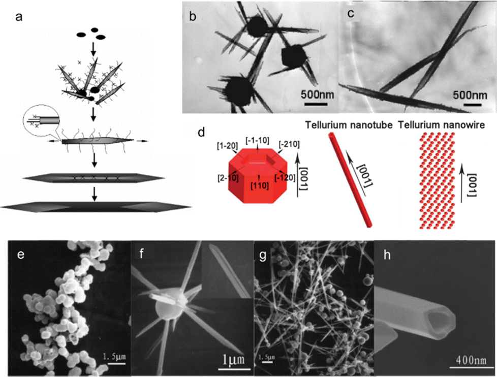
The shape and size of tellurium nanocrystals are crucial in determining their properties and applications. During the solution synthesis of Te nanostructures, controllable morphological transformations, including size change and shape variations, are widely explored to obtain various Te nanocrystals.55,58–62 As shown in Fig. 1, Te seeds are typically generated by the chemical reduction of Te source, such as sodium tellurite, orthotelluric acid, and tellurium dioxide, using reductants like hydrazine hydrate and glucose. Due to its inherent anisotropy, the trigonal crystal structures tend to grow along the c-axis. With the assistance of surfactants, morphological evolution from 1D to 2D forms can be realized. Preparation parameters, including reaction temperature, reaction time, reactant mole ratio, and reaction media, play significant roles in determining the morphology of the synthesized Te nanostructures. Precise control of preparation parameters has been investigated by many research works to explore the diversity and controllability of Te nanostructures, enabling the designable formation of Te nanowires, nanotubes, nanobelts, nanocables, and tellurene.9 The morphology-controlled syntheses of Te nanostructures are summarized in Table 1.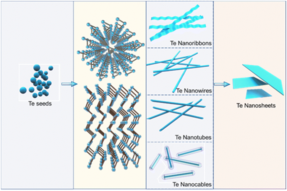 | ||
| Fig. 1 Schematic of the morphological evolutions and transformations of Te nanostructures. | ||
| Te source | Reductant | Surfactant | Reaction media | Additional condition | T (°C) | RT (h) | Morphology | Ref. |
|---|---|---|---|---|---|---|---|---|
| Na2TeO3 | Hydrazine hydrate | — | HCl | — | 100 | 12 | Nanowires | 63 |
| — | NaOH | — | Tubular structure | |||||
| PVP | 0.1 g PVP | Sphere | ||||||
| 0.05 g PVP | 48 | Nanowires | ||||||
| 0.01 g PVP | 48 | Bow-like microcrystals | ||||||
| TeO2 | Hydrazine hydrate | PVP | Ammonia | — | 200 | 4 | Nanowires | 14 |
| 12 | Nanosheets | |||||||
| Na2TeO3 | Glucose | — | DI water | — | 90 | 12 | Nanotubes | 64 |
| 120 | Nanowires | |||||||
| 180 | Nanocables | |||||||
| Na2TeO3 | Glucose | CTAB | DI water | — | 130 | 12 | Nanowires | 65 |
| 90 | Nanoparticle | |||||||
| 110 | Nanorod | |||||||
| — | 170 | Nanocables | ||||||
| Na2TeO3 | Hydrazine hydrate | PVP | Ammonia | 0.5 g PVP | 180 | 4 | Nanoparticle | 66 |
| 1.0 g PVP | Nanowires | |||||||
| 1.5 g PVP | Nanosheets | |||||||
| TiO2 | Ethylene glycol | — | NaOH | — | 170 | 0.42 | Nanowires | 67 |
| 200 | Nanotubes | |||||||
| Orthotelluric acid | Ethylene glycol | — | Pure water | 40 mM orthotelluric acid | 197 | 2 | Nanotubes | 53 |
| 0.7 mM orthotelluric acid | Nanowires | |||||||
| Na2TeO3 | H2O | — | Ammonia | 0.0005 M Na2TeO3 | 220 | 36 | Nanorod | 68 |
| 180 | ||||||||
| 0.005 M Na2TeO3 | Nanobelts; nanotubes; nanorods | |||||||
| Na2TeO3 | H2O | — | Serine | — | 160 | 12 | Nanotubes | 69 |
| Lysine | Nanowires | |||||||
| Histidine | Dendritic crystals | |||||||
| Te powder | — | — | — | Hydrazine hydrate as medium | 160 | 6 | Nanowires | 70 |
| HCl | 12 | Nanotubes | ||||||
| TiO2 | Glucose | Glucose | NaOH | 180 | 1 | Nanoplates | 71 | |
| 5 | Nanowires | |||||||
| 10 | Nanospheres | |||||||
| Orthotelluric acid | Ethylene glycol | — | Pure water | Morphology is controlled by the refluxing temperature | <100 | — | Spines | 72 |
| 100–160 | Filaments | |||||||
| 160–180 | Needles | |||||||
| >180 | Tubular structures |
Liu et al. used sodium tellurite (Na2TeO3) and hydrazine hydrate as the Te source and reductant respectively, achieving Te nanospheres, Te NWs, Te tubular structure and bow-like nanostructure by changing surfactants, reaction media and reaction time.63 In the reaction media of acidic (HCl) solution, nanowires with diameters ranging from 30 to 100 nm and lengths of tens of micrometers were generated (Fig. 2(a)). While in the reaction of alkaline (NaOH) solution, tubular crystals show up with 1–2 μm in diameter and several hundred micrometers in length (Fig. 2(b)). Due to the lower rate of reduction reaction in alkaline media, Te atoms are insufficient for the growth of the central part with relatively lower free energies than circumferential edges of each seed, leading to the formation of the tubular structure. The shape of the products is determined by the reaction media. Meanwhile, their size could also be modulated by the concentration of reaction media. Furthermore, the addition of surfactant (polyvinyl pyrrolidone, PVP) has a great influence on the morphology of the obtained Te nanostructures by absorbing on the surface of the initial Te particles to obstruct Te diffusion. Therefore, Te spheres (∼100 nm in size) were formed after growing for 12 h with 0.1 g PVP (Fig. 2(c)), Te nanowires (∼20–30 nm in diameter) came out after growing for 48 h with 0.05 g PVP (Fig. 2(e)), and Te bow-like structures were generated after growing for 48 h with 0.01 g PVP (Fig. 2(d)). Wang et al. also demonstrated the formation of Te nanostructures by modulating the amount of PVP (Fig. 3(a)). Besides, temperature is another crucial factor for the morphology of the synthesized Te nanostructures. When the temperature increases from 100 °C to 125 °C with 0.1 g PVP, the final products change from nanowire to bow-like structures with irregular surfaces (Fig. 2(f)).
 | ||
| Fig. 2 (a) Scanning electron microscope (SEM) image of Te NWs prepared in acidic solution with 1 M HCl. (b) SEM image of Te tubular structure prepared in alkaline solution with 1 M NaOH. (c) SEM image of uniform Te spheres prepared in 1 M of NaOH aqueous solution and 0.1 g of PVP. (d)–(f) Morphologies of synthetic Te nanostructures with different amounts of PVP and different temperatures. (d) 0.01 g of PVP, at 100 °C for 48 h; (e) 0.05 g of PVP, at 100 °C for 48 h; and (f) 0.1 g of PVP, at 125 °C for 48 h. Reproduced with permission.63 Copyright 2003, The Royal Society of Chemistry. (g)–(j) SEM images of synthetic Te nanostructures with different reaction times: (g) 1 h (nanoplates); (h) 3 h (a mixture of Te NWs and nanoplates); (i) 5 h (Te NWs dominant); (j) 10 h (Te nanospheres). Reproduced with permission.71 Copyright 2020, Springer. (k)–(m) SEM images of synthetic Te NWs (g), Te NTs (h), and Te dendritic crystals (i) in the presence of different additives. Reproduced with permission.69 Copyright 2005, American Chemical Society. | ||
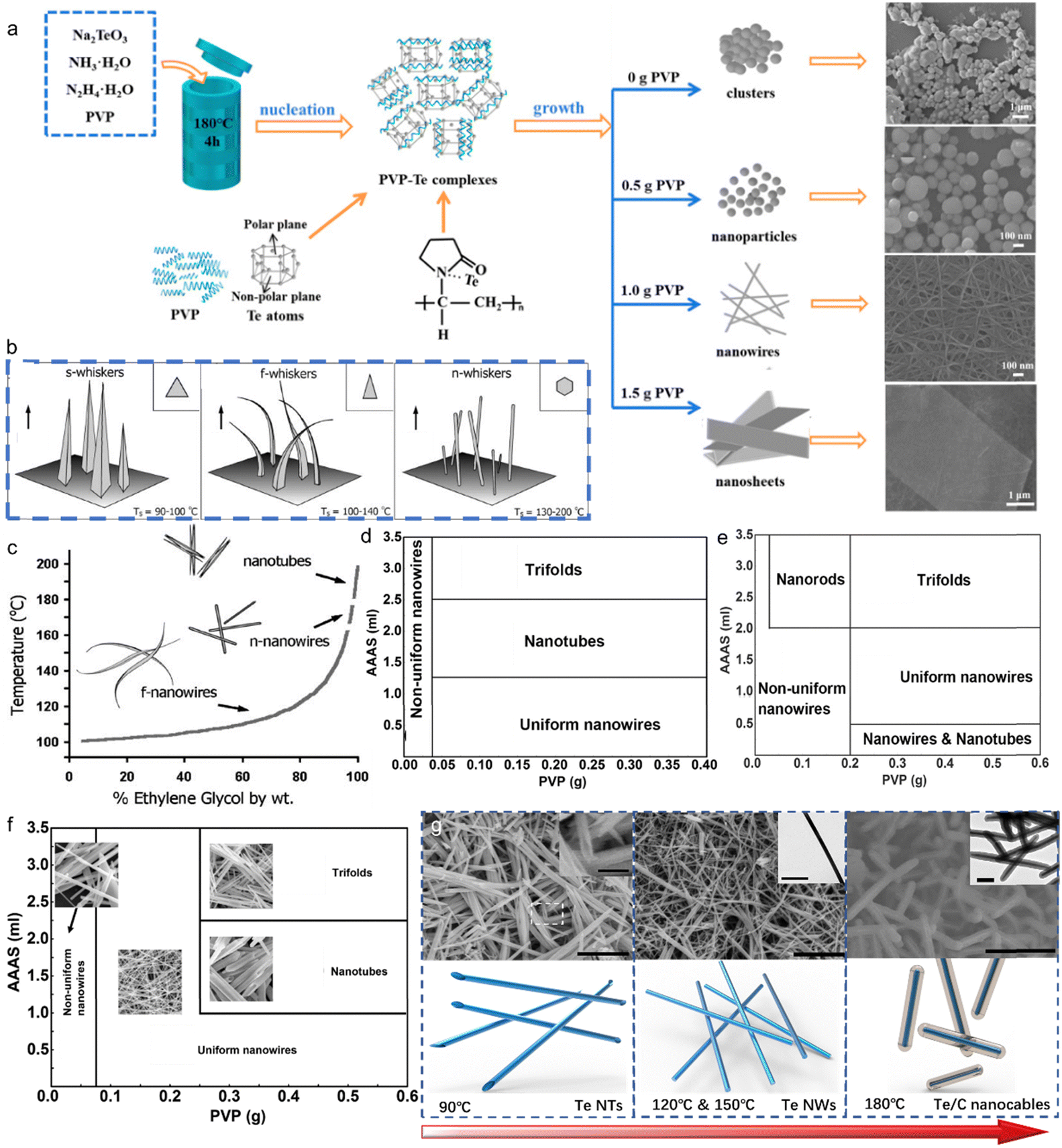 | ||
Fig. 3 (a) Schematic of the formation processes of various Te nanostructures with different amounts of PVP. Reproduced with permission.66 Copyright 2023, MDPI. (b) Schematic of different Te whiskers. (c) The boiling points of EG and water mixtures as a function of the ratios of EG![[thin space (1/6-em)]](https://www.rsc.org/images/entities/char_2009.gif) :water. In the range of 174 °C to 182 °C, needle-shaped Te NWs were obtained, below 174 °C filamentary Te NWs were formed and Te NTs were generated above 182 °C. Reproduced with permission.72 Copyright 2002, The Royal Society of Chemistry. (d)–(f) Morphological evolution of Te nanostructures with different amounts of PVP and AAAS at (d) 120 °C, (e) 150 °C and (f) 180 °C. Reproduced with permission.73 Copyright 2017, The Royal Society of Chemistry. (g) Schematic of different Te nanostructures synthesized at different temperatures. Reproduced with permission.64 Copyright 2023, The Royal Society of Chemistry. :water. In the range of 174 °C to 182 °C, needle-shaped Te NWs were obtained, below 174 °C filamentary Te NWs were formed and Te NTs were generated above 182 °C. Reproduced with permission.72 Copyright 2002, The Royal Society of Chemistry. (d)–(f) Morphological evolution of Te nanostructures with different amounts of PVP and AAAS at (d) 120 °C, (e) 150 °C and (f) 180 °C. Reproduced with permission.73 Copyright 2017, The Royal Society of Chemistry. (g) Schematic of different Te nanostructures synthesized at different temperatures. Reproduced with permission.64 Copyright 2023, The Royal Society of Chemistry. | ||
Unlike general morphological evolution, Cui et al. performed morphological evolution from 2D Te nanoplates to Te NWs and Te nanospheres by controlling the reaction time.71 In the hydrothermal growth reaction, TiO2 was reduced by NaOH and glucose. As shown by Fig. 2(g)–(j), with the reaction time increasing, the products changed gradually from Te nanoplates to Te nanospheres. Organic molecules with specific functional groups play a great role in the growth of inorganic crystals. Several amino acids with different structural conformations and functionalities were selected by He et al.69 to control the shape and size of the synthesized Te nanostructure in hydrothermal processes. The surface tension of Te products could be modified by amino acids. In the presence of serine, shuttle-like nanotubes with a diameter of ∼500 nm and length of several micrometers were synthesized, as shown in Fig. 2(l). In contrast, if one extra amino group was supplied by lysine, the final products turned into superlong rigid nanowires with length over 100 μm and a uniform diameter of 150 nm (Fig. 2(k)). However, the employment of another amino acid, histidine, containing one carboxyl, one amino group and a penta-ring, produced dendritic crystals of Te with branched nanorods as shown in Fig. 2(m). Xia et al.72 performed a solution-phase, self-seeding method to synthesize various 1D Te nanostructures through the reduction of orthotelluric acid by hydrazine at different refluxing temperatures. Fig. 3(b) exhibits the different Te whiskers grown by the different temperatures. In Fig. 3(c), the refluxing temperature was modulated by adding different amounts of water in ethylene glycol (EG), and the morphology of the final Te nanostructure was also determined. When the refluxing temperature is lower than 100 °C, spine-shaped crystals (or s-whiskers) were obtained. In the range of 174 °C to 182 °C, needle-shaped Te NWs were obtained, below 174 °C filamentary Te NWs were formed and Te NTs were generated above 182 °C. Zhang et al.73 synthesized Te NWs, Te NTs, and trifold nanorods using an environmentally benign solvothermal approach using non-hazardous ascorbic acid as a reductant, PVP as surfactant and ethylene glycol as solvent. Fig. 3(d)–(f) shows the prepared Te nanostructures at different temperatures using different amounts of PVP and ascorbic acid aqueous solution (AAAS). The explorations of temperature as a pivotal factor affecting the morphology of the products were performed by Xu et al.64 The biomolecule glucose replaced toxic hydrazine hydrate as a reducing agent in the hydrothermal process, so green synthesis of various Te nanostructures was realized by precisely modulating temperature (Fig. 3(g)). When the chemical reaction takes place at low temperature (90 °C), insufficient Te atoms were provided by the slow reduction reaction. The finite Te atoms accumulated at the circumferential edges of each seed with higher free energies to form Te nanotube with a diameter of ∼80 nm and a length of several micrometers. When the reaction temperature increases to 120 °C, the reduction reaction processes more rapidly to produce enough Te atoms for the growth of the central part of the initial Te particles, so Te nanowires with ∼25 nm in diameter were the final products. If the preparation was raised to 180 °C, which is higher than the glycosidation temperature of glucose, the carbonization of glucose led to the formation of an amorphous layer on the surface of Te nanowires, and the final products appeared as Te/C nanocables with the outer shell (ca. 30 nm) and the inner core (ca. 25 nm).
The 1D to 2D transition in tellurium is an essential section for the solution process of preparing tellurene, due to its specific helical chains. By using four-dimensional scanning transmission electron microscopy (4D-STEM), Alejandra et al. studied the transition from 1D to 2D tellurium phase in a microwave-enhanced synthesis process.74 As demonstrated in Fig. 4(a), as evidenced by X-ray diffraction (XRD) patterns, ultrathin Te nanowires are first observed at the reaction temperature of 150 °C. For the microwave temperature of 175 °C, a mixture of thin and thicker Te nanowires was identified. When the reaction temperature increases to 190 °C, the observed product is a mixture of thick Te NWs plus 2D flakes. While Te nanoribbons and 2D flakes could be obtained at the optimal reaction temperature of 180 °C and a decreasing Na2TeO3:PVP ratio from 54 to 34, as exhibited in Fig. 4(b). Fig. 4(c) is a typical high-angle annular dark-field STEM image of the synthesized 2D tellurene. The curves of (β*/q)2versus (β*/q2) are plotted in Fig. 4(d), in which the slope represents the inverse of the coherent domain size and the intercept is the square root of the apparent nanostrain ε. The calculated coherent domain size increases with the products become larger and transition from 1D to 2D phase.
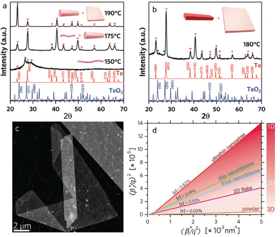 | ||
| Fig. 4 (a) XRD patterns of Te nanostructures prepared at different temperatures with a Na2TeO3:PVP molar ratio of 54. (b) XRD patterns of Te nanostructures prepared at 180 °C with a Na2TeO3:PVP molar ratio of 34. (c) High-angle annular dark-field STEM image of 2D Te nanosheets. (d) Halder–Wagner graph of Te nanostructures by 4D-STEM in comparison with that calculated for bulk powders by XRD. Reproduced with permission.74 Copyright 2020, Wiley-VCH GmbH. | ||
3. Growth mechanisms for Te nanostructures
To understand the underlying exotic theory for the morphological evolutions of Te nanostructures, various reasonable growth mechanisms based on different conditions have been proposed based on the experimental characterizations. Researchers explored the morphological evolutions of Te nanostructures from 0D to 1D to 2D phases and the morphological transformations between them. Some subtle but critical differences exist in the Te nanostructures with similar morphologies, such as shuttle-like Te NTs, Te NTs with cylindrical seeds, belt-rolled Te NT. Critical mechanisms are indispensable to illustrate the underlying growth theories and provide guidance for experimental works.Xia et al. proposed a concentration depletion mechanism at the surface of the cylindrical seeds to describe the growth of Te NTs in the polyol process75 and morphology transformation of Te nanostructures.53 The transmission electron microscopy (TEM) images in Fig. 5(a) show the growth process of Te NTs at different stages, beginning with the formation of cylindrical seeds and subsequent growth along their circumferential edges. Fig. 5(b)–(d) illustrates the SEM images of the morphological transformation of Te 1D nanostructures with varying concentrations of orthotelluric acid. As the concentration of orthotelluric acid decreased from 40 to 8 and 0.7 mM, the sizes of the initial Te seeds changed from 260 to 120 and 50 nm. Since the wall thickness (∼30 nm) of the synthesized Te NTs is constant (determined by the diffusion length of Te atoms on the seed surfaces), when the radius of Te seed is comparable to the diffusion length, the Te products evolved from nanotubes to nanorods. The schematic diagrams on the right side of Fig. 5(b)–(d) illustrate the growing face of a Te seed. A mixture of tellurium nanobelts, nanotubes, and nanorods was synthesized by reducing sodium tellurite in an aqueous ammonia system at ∼180 °C.68 Most Te nanobelts are very thin and uniform in thickness and width along their entire length, as shown in Fig. 5(e). The average thickness of Te nanobelt is ∼8 nm, similar as the average thickness (ca. 8 nm) of Te nanotubes whose thicknesses are in the range of 5–20 nm. Some Te nanobelts show twisting (Fig. 5(e)), some Te nanotubes end in tail-like helical belts (Fig. 5(f)), and some Te nanotubes show helical nanobelt-lined structures (inset in Fig. 5(f)). The helical belt template mechanism is proposed to explain the formation of the tellurium nanotubes. Using the helical nanobelt as the template, the relatively wider nanobelt rolls up around the twisted helical belt, the so-called template-roll growth (the upper schematic in Fig. 5(g)). The lower schematic in Fig. 5(g) explains the template-twist-join growth that is the twisting nanobelt grows through “epitaxy” along its edges and joins both the side edges of itself and evidenced by the tail-like structure in Fig. 5(f).
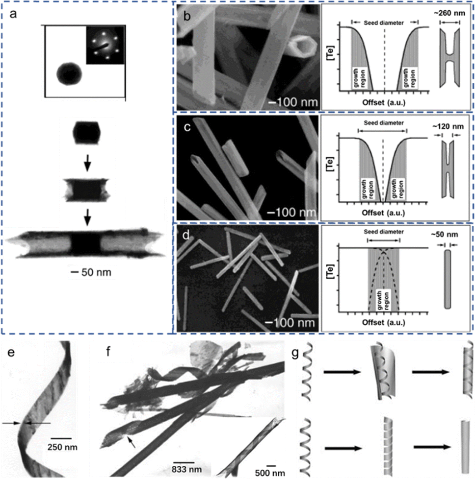 | ||
| Fig. 5 (a) Upper: Cross-sectional TEM image of a cylindrical seed and the microdiffraction pattern of this seed. Lower: TEM images of Te NTs at different stages of growth. (b)–(d) Left: SEM images of synthesized Te NMs with different concentrations of orthotelluric acid in ethylene glycol: (b) 40, (c) 8, (d) 0.7 mM. Right: Schematic diagram of the growing face with each concentration. Reproduced with permission.53 Copyright 2002, WILEY-VCH Verlag GmbH. (e) TEM image of synthesized lightly twisted Te NR. (f) TEM image of belt-twisted Te NTs. Inset is the belt-rolled Te NT. (g) Schematic diagram of the proposed formation mechanisms for the synthesized Te NTs. Upper: Template-roll-growth mechanism. Lower: Template-twist-join-growth mechanism. Reproduced with permission.68 Copyright 2002, WILEY-VCH Verlag GmbH. | ||
A scrolling mechanism is proposed by Yu et al. to illustrate the formation of shuttle-like Te NTs (Fig. 6(a)) in the presence of serine.69 Initially, amorphous Te nanoparticles form, followed by the growth of bamboo leaf-like nanostructures on their surfaces, as shown by the TEM image in Fig. 6(b). These nanotubes peel off from the amorphous matrix and grow further along the Ostwald ripening process. Epitaxial growth takes place with further adsorption of amorphous nanoparticles. The extended layers rolled with the influence of gravity and charge interaction between internal and external layers until the middle parts joined together, resulting in the formation of shuttle-like nanotubes (Fig. 6(c)). Li et al. summarized the growth mechanism of tellurium nanowires and nanotubes synthesized by employing ethylene glycol as the reductant and TiO2 as the tellurium source in the presence of NaOH.67 Na2TeO3 is first formed as the intermediate product. At 155 °C, due to the excess absorption of Na2TeO3, Te atoms occur very slowly in (001) and (110) planes, leading to the growth of nanocylinders with pits at both ends (left in Fig. 6(d)). At 170 °C, the Na2TeO3 concentration is very low due to the rapid growth of (001) plane, which results in the direct growth of Te nanowire (right in Fig. 6(d)). Above 185 °C, the Na2TeO3 concentration increases significantly and the Te nanocylinders grow into Te nanotubes (middle in Fig. 6(d)) along the [001] direction based on the anisotropic crystal structure of Te. Fig. 6(e)–(h) demonstrate the growth process of Te nanotubes observed by Qian et al. using sodium tellurate (Na2TeO4·2H2O) and formamide (HCONH2) as tellurium source and reductant, respectively.76 Different from the Te nanotubes prepared by Xia et al.53 and Qian et al.,68 no cylindrical seeds were observed inside the hollow structures. A nucleation–dissolution–recrystallization mechanism describes the formation of Te nanotubes. Initially, t-Te sphere-like crystals instead of α-Te are formed due to the very slow rate of nucleation, which would dissolve to provide Te atoms for the growth of groove-like nanorods on their surfaces (inset in Fig. 6(f)). The slow dissolution process cannot provide sufficient Te atoms for the growth of the central in nanorods. The incomplete nanotube structures indicate that the tuber axis directional growth rate is faster than the circumferential directional rate. With reaction time prolonged, Te nanoparticles disappear and are completely converted into nanotubes. However, prongs exist at the ends of Te nanotubes, which will grow into perfect nanotubes with reaction lasts long enough (Fig. 6(h)).
 | ||
| Fig. 6 (a) Schematic illustration of the proposed growth mechanism of the shuttle-like Te NTs using serine. (b) TEM image of the bamboo-like Te nanostructure living on the aggregated amorphous Te particles. (c) TEM image of the intact shuttle-like Te NTs. Reproduced with permission.69 Copyright 2005, American Chemical Society. (d) Schematic diagram of growth mechanisms for Te NTs and Te NWs. Reproduced with permission.67 Copyright 2013, The Royal Society of Chemistry. (e)–(h) SEM images of products after hydrothermal treatment for (e) 5 h, (f) 8 h, (g) 12 h, and (h) 20 h. Reproduced with permission.76 Copyright 2005, American Chemical Society. | ||
Large area and high-quality 2D tellurium was synthesized by Wu et al. utilizing a hydrothermal approach.77 The process-tunable thicknesses range from a monolayer to tens of nanometers, with lateral sizes of up to 100 μm. The optical image in Fig. 7(a) displays the morphology of the synthesized tellurene, and the inset is a typical solution dispersion. A detailed morphology transformation from 1D to 2D nanostructures is elucidated and shown by the schematic in Fig. 7(b). The crystal-face-blocking ligand PVP is preferentially adsorbed on the {10![[1 with combining macron]](https://www.rsc.org/images/entities/char_0031_0304.gif) 0} surfaces of the initially formed Te seeds,78 promoting the formation of 1D nanostructure. After a period of reaction, because of the insufficient PVP capping, the growth of {100} surfaces along the 〈1
0} surfaces of the initially formed Te seeds,78 promoting the formation of 1D nanostructure. After a period of reaction, because of the insufficient PVP capping, the growth of {100} surfaces along the 〈1![[2 with combining macron]](https://www.rsc.org/images/entities/char_0032_0304.gif) 10〉 significantly increases through thermodynamic-driven assembly due to its lowest free energy.79 The simultaneous growth along the 〈110〉 and 〈0001〉 direction leads to the emergence of 2D tellurium. PVP concentration is a pivotal factor in this synthesis process of tellurene. Fig. 7(c) shows the productivity as a function of reaction time with different Na2TeO3/PVP mole ratios. After 1.5 hours, the products are in 1D form for all PVP concentrations. With reaction time prolonging, the productivity of tellurene keeps growing until it reaches saturation after processing for 30 hours. A lower level of PVP promotes the rapid growth of tellurene (∼2 hours) but also results in smaller final productivity. Tellurene with a thickness of less than 10 nm could be achieved by a solvent-assisted post-growth thinning process. Fig. 7(d) shows the thinning results confirmed by atomic force microscope AFM. Large-area tellurene with monolayer, bilayer, and few-layer thicknesses have been obtained by changing the pH values of the tellurene solution in the post-growth thinning process.
10〉 significantly increases through thermodynamic-driven assembly due to its lowest free energy.79 The simultaneous growth along the 〈110〉 and 〈0001〉 direction leads to the emergence of 2D tellurium. PVP concentration is a pivotal factor in this synthesis process of tellurene. Fig. 7(c) shows the productivity as a function of reaction time with different Na2TeO3/PVP mole ratios. After 1.5 hours, the products are in 1D form for all PVP concentrations. With reaction time prolonging, the productivity of tellurene keeps growing until it reaches saturation after processing for 30 hours. A lower level of PVP promotes the rapid growth of tellurene (∼2 hours) but also results in smaller final productivity. Tellurene with a thickness of less than 10 nm could be achieved by a solvent-assisted post-growth thinning process. Fig. 7(d) shows the thinning results confirmed by atomic force microscope AFM. Large-area tellurene with monolayer, bilayer, and few-layer thicknesses have been obtained by changing the pH values of the tellurene solution in the post-growth thinning process.
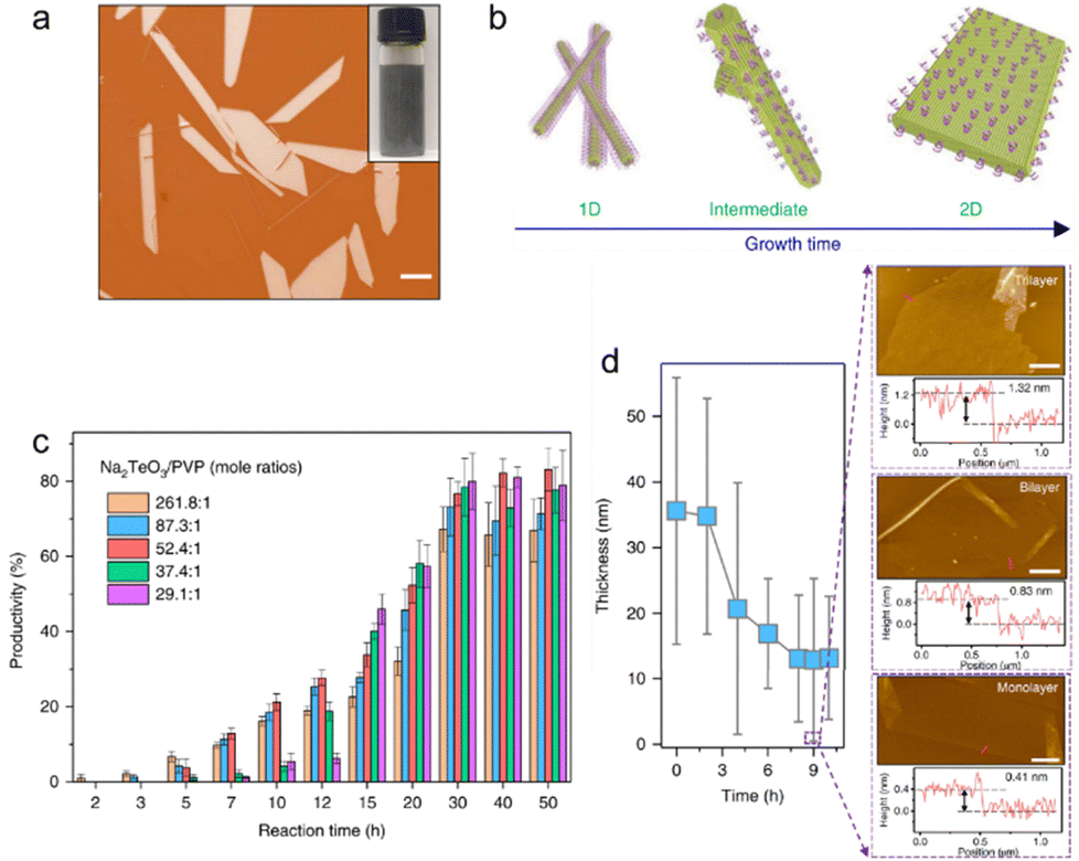 | ||
| Fig. 7 (a) Optical image of solution-phase grown Te nanosheets. Scale bar, 20 μm. Inset, upper right is the optical image of Te nanosheets solution and lower left is the atomic structure of tellurium. (b) Schematic diagram of the morphological evolution from 1D to 2D Te nanostructures. (c) Productivity of Te flakes as a function of reaction time with different PVP concentrations. Error bars represent s.d. (d) The thickness variation of Te nanosheets with different post-growth thinning treatment times. The right AFM images illustrate few-layer and monolayer Te flakes. Scale bar, 5 μm. Reproduced with permission.77 Copyright 2018, Macmillan Publishers Limited, part of Springer Nature. | ||
Sun et al. systematically investigated the growth mechanism of hydrothermal synthesized Te nanosheets by employing TEM.14 The obtained Te nanosheets could be represented by three typical shapes, as shown in Fig. 8(a)–(c). Type i is a trapezoidal configuration grown along the directions of [0001] and [110], showing an interior angle of 37°, commonly used for optoelectronic applications.80 Type ii Te nanosheet looks like the combination of two type i nanosheets along their short sides. Type iii nanosheet is a symmetrical “V” shape with an included angle of 41°. Fig. 8(d) summarizes the proportions of three types of Te nanosheets after different reaction times. Initially, type ii Te nanosheets dominate the product. As the reaction time increases, the proportion of type ii decreases from 66.7% to 11.4%, type i increases from 22.2% to 86.8%, and type iii is always low (from 11.1% to 1.8%). Moiré fringes are observed at the middle region framed in the white box in Fig. 8(b), and the spacing is measured to be around 2.03 nm (Fig. 8(e)). The Moiré fringes are supposed to be attributed to the edge superposition of two nanoflakes. While no Moiré fringe appears at the interfacial region of type iii Te nanosheet (Fig. 8(f)).
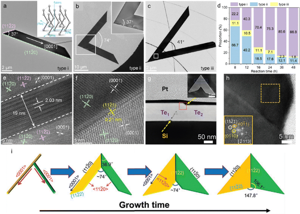 | ||
| Fig. 8 (a)–(c) Three typical types of Morphologies for the synthetic Te nanosheets. Inset in (a) is the atomic structure of tellurium. (d) Proportions variation of different types with different reaction times. (e) high-resolution TEM image of Moiré fringes at the interfacial region of the overlapping part. (f) Atomistic structures of the interfacial boundary for type iii. No Moiré fringe is observed. Reproduced with permission.14 Copyright 2023, American Chemical Society. (g) High-angle annular dark-field STEM image of Te flake cross-section as marked by the blue boxed region in the inserted SEM image. (h) high-resolution TEM image of area framed by the red dotted box in (g). Inset is the fast Fourier transforms of the dash boxed region. (i) Schematic illustration of the morphological evolution from the crossed Te nanowires to symmetrical Te nanoflake. Reproduced with permission.81 Copyright 2021 Wiley-VCH GmbH. | ||
To demonstrate the superposition of the contacting nanoflakes directly, Gao et al. investigated the cross-sectional view of the synthesized symmetric Te nanosheet.81 The specific region marked by the blue box in the inset of Fig. 8(g) shows Moiré fringes and its cross-sectional view is exhibited by the SEM image in Fig. 8(g). Clear boundaries could be observed at the interface of two separated flakes named Te1 and Te2, as marked by the yellow dashed arrow. The overlapped area between Te1 and Te2 results in the formation of Moiré fringes. Fig. 8(h) is the high-resolution TEM image of the interface region framed with the red dotted box in Fig. 8(g), indicating that Te1 and Te2 are tightly bound with good crystallinity. A possible morphological transformation from 1D to 2D form is elucidated in Fig. 8(i). Two Te nanowires intersect and stretch out at the intersection, followed by the thermodynamic-driven continuous growth along the 〈110〉 and 〈0001〉 directions due to the insufficient PVP capping. Meanwhile, the lateral extension along each 〈110〉 direction occurs based on the intersected nanowires, which could lead to slight differences in thickness and overlapping between the two grown Te flakes (Fig. 8(g)). Finally, Te nanosheets with different shapes are obtained.
4. Applications of Te nanostructures
Two-dimensional tellurium possesses a thickness-dependent band gap from 0.31 eV to 1.26 eV, holding great promise for broadband photo detection.82,83 Furthermore, simulation works confirmed that the morphology of Te nanostructure has a slight effect on its light absorption.4 Zhu et al. calculated the effective mass of hole and electron using phonon finite method, which is and
and 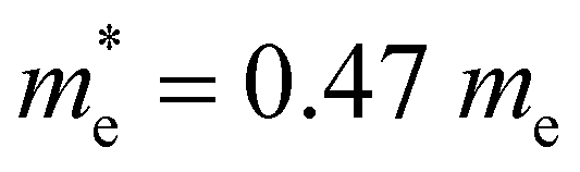 , respectively,84 indicating high mobility (∼1000 cm2 V−1 s−1) as observed by experimental works.77 Stability is another pivotal property for the applications of Te nanostructures. Both theoretical85 and experimental77 investigations demonstrated thermodynamic and air stability. Te nanostructures exhibit a special chiral-chain structure, which results in anisotropy properties, novel gyrotropic properties, and complex band structures with Weyl crossings.86,87 The above properties of Te nanostructures provide an ideal platform for novel chiral-related optics and optoelectronic devices.
Based on their intriguing properties, Te nanostructures have been explored for a number of applications.88–93 The comprehensive applications of Te nanostructures have been summarized recently.4,94 Here, a summary of very recent application works of Te nanostructures is demonstrated. A stretchable and flexible thin-film transistor was achieved based on the wafer-scale Te NWs with high-mobility and stretchability (Fig. 9(a)).95 The highly oriented arrays of Te NWs were assembled by a facile lock-and-shear strategy that mimics the alignment method of the trailing tentacles of a swimming jellyfish (Fig. 9(b)). On/off ratios of ∼104 and mobilities over 100 cm2 V−1 s−1 are obtained by Te NWs thin-film transistor. A vertical pn and Schottky junction was formed at the interface of 2D WS2 and Te nanoribbon96 (Fig. 9(c)). Thus the dark current and electric noise were suppressed because of the formation of depletion region in WS2 and the specific detectivity has been enhanced two orders of magnitude compared to the pristine WS2 device. Liu et al. fabricated a flexible multifunctional thermoelectric device using ordered Te–Au hetero-NW film (composed of Te NWs and Au nanoparticles).97 As shown by the schematic in Fig. 9(d), the achieved multifunctional thermoelectric detector can effectively detect object and environment temperature, heat proximity, airflow and thermal conductivity. Fig. 9(e) is the TEM image of the Te–Au hetero-nanowire film. Yu et al. observed the negative photoconductance by p-type Te NWs film, which is supposed to be attributed to the absorbed oxygen on the surface of Te NWs.98 Enlarged optical intensities from the UV to VIS-IR region with both negative and positive photoresponse were reported (Fig. 9(f)). Twisted heterostructures based on Te/MoS2 were utilized for an ultrasensitive photodetector (Fig. 9(g)), and the interfacial band alignment can be engineered by the tailoring the lattice mismatch and distance.99 The photocurrent is significantly enhanced by the interface alignment. A self-rolled Te photothermoelectric detector was fabricated by Huang et al., as shown in Fig. 9(h).100 The high light absorption and localized thermal energy of the 3D tubular structure enhanced the photothermoelectric effect and corresponding photodetection performance of the Te-based detector. Furthermore, tubular Te photodetector demonstrates ultrawide-angle detection and a stable broadband polarization-dependent photoresponse.
 | ||
| Fig. 9 (a) Schematic of a flexible Te NWs thin film transistor. (b) Schematic diagram of the aligning process of the wafer-scale Te NWs arrays. Reproduced with permission.95 Copyright 2024, AAAS. (c) Schematic illustration of WS2/Te NR photodetector. Reproduced with permission.96 Copyright 2024 AIP Publishing. (d) Schematic of the flexible multifunctional thermoelectric device based on the ordered Te–Au hetero-NW film. (e) TEM image of ordered Te–Au hetero-NW film. Reproduced with permission.97 Copyright 2024 Wiley-VCH GmbH. (f) Output curves of Te NW film with and without laser illumination (365 nm). Inset is the schematic illustration of Te NW photodetector. Reproduced with permission.98 Copyright 2022 Wiley-VCH GmbH. (g) Optical images of three different types of tellurene/MoS2 heterostructures: “parallel” stacking (left); “misorientation” stacking (middle); “vertical” stacking. Lower images are top-view schematics of each stacking. Reproduced with permission.99 Copyright 2023 Wiley-VCH GmbH. (h) Schematic of self-rolled Te photothermoelectric detector. Reproduced with permission.84 Copyright 2024 Springer Nature. | ||
Multiple applications of tellurene in different fields have been widely investigated.101–105 A nonvolatile optoelectronic memory was fabricated by ReS2/hBN/2D Te heterostructures, in which tellurene worked as the floating gate (Fig. 10(a)).38 Multi-bit storage states (Fig. 10(b)) can be realized by changing the gate voltage and Boolean logic gate operations (OR and AND) have been successfully performed by applying optical and electrical inputs. Tunable negative photoconductivity was obtained by the Al2O3-encapsulated tellurene photodetectors with excellent photoresponsivity of up to 6.9 × 10⁴ A W−1 (Fig. 10(c)).80 By depositing the Al2O3 top layer, ambipolar transporting property was shown by tellurene photodetector, and its carrier mobility is reduced by the enhanced phonon scattering due to the photothermal effect, leading to the negative photoconductivity and high performance. A single-crystalline tellurene flexible synaptic transistors were fabricated by Lee et al.,106 (Fig. 10(d)) which exhibit considerably low power consumption of 9 fJ, 93 effective multilevel states and excellent symmetry and linearity. Li et al.107 used a mild oxidative thinning strategy to achieve thin tellurene flakes and fabricated a four-terminal device using p-type tellurene and n-type ReS2 (Fig. 10(e)). A rectification ratio of 103 was shown by the ReS2/Te p–n diode. The magnetoresistance and nonreciprocal transport property of tellurene were investigated by Wang et al. (Fig. 10(f)).108 An unreported negative magnetoresistance was observed in the weak magnetic field of 0–2 T due to the participation of the Weyl nodes in the transport (Fig. 10(g)). Furthermore, a perpendicular spin component is detected in the Fermi surface near the Weyl nodes. Large-scale and high-pixel-density 2D imaging unit arrays were fabricated by Yang et al. using wafer-scale tellurene (Fig. 10(h)).41 Wide-spectrum photoresponse from 370.6 to 2240 nm and high responsivity 2.7 × 10⁷ A W−1 were obtained.
 | ||
| Fig. 10 (a) Schematic illustration of a logic gate based on ReS2/hBN/2D Te heterostructures. (b) Laser-controlled multi-bit storage of memory device based on ReS2/hBN/2D Te heterostructures. Reproduced with permission.38 Copyright 2024, American Chemical Society. (c) Transfer curves of Al2O3-encapsulated tellurene photodetectors with and without laser illumination (450 nm). Inset is the schematic illustration of Al2O3-encapsulated tellurene photodetectors. Reproduced with permission.80 Copyright 2023 Elsevier Ltd. (d) Schematic of the single-crystalline tellurene flexible synaptic transistors. Reproduced with permission.106 Copyright 2024, The Royal Society of Chemistry. (e) Schematic diagram of ReS2/2D Te heterostructures. Reproduced with permission.107 Copyright 2024 Wiley-VCH GmbH. (f) Schematic of tellurene device. (g) Schematic of Adler–Bell–Jackiw effect of Weyl nodes in the B||E configuration. Reproduced with permission.108 Copyright 2024 American Chemical Society. (h) Schematic of tellurene photodetector. Reproduced with permission.41 Copyright 2023 Wiley-VCH GmbH. | ||
5. Conclusions
Tellurium nanostructures possess specific chiral-chain structures and can be synthesized using template-free solution-phase approaches, allowing for controllable morphologies and dimensions. However, the use of toxic reductants and additional surfactants in these processes threatens the environment and can leave residues on the surface of Te nanomaterials, thereby reducing their properties. Green liquid-phase synthesis without surfactant offers an effective approach to enhance the quality of the obtained Te nanostructures.109 Furthermore, mechanical exfoliation generally gives the intrinsic properties of nanosheets without the influence of solvents. The properties of the mechanically exfoliated tellurene should be investigated and demonstrated, maybe with the assistance of annealing. Currently, 1D Te nanostructures, including Te NWs, Te NTs, and Te NRs, can grow into Te nanosheets.77,110,111 However, a post-growth process is still needed to obtain ultrathin 2D tellurium. Direct growth of ultrathin and large-area Te nanoflakes may be realized by modifying the morphology and dimensions of the 1D precursors. Furthermore, the obvious structure lattice orientation of liquid synthesized and even mechanically exfoliated Te nanostructures facilitates the study of twisted heterostructures and novel optoelectronic devices.In conclusion, tellurium nanostructures are fascinating materials with exceptional properties and a wide range of applications. Continued efforts in understanding and controlling the growth mechanisms are essential for high-quality tellurium-based nanomaterials and their integration into advanced technological applications.
Data availability
Data availability is not applicable to this article as no new data were created or analyzed in this study.Conflicts of interest
There are no conflicts to declare.Acknowledgements
We gratefully acknowledge support from the National Natural Science Foundation of China (grant no. 62105018 and 61975007), the Fundamental Research Funds for the Central Universities 2021RC212, Beijing Natural Science Foundation of China (grant no. Z190006 and 4222073), the National Research Foundation of Korea (NRF) (grant no. 2021R1A2C1012176).References
- C.-H. Yin, H.-W. Fang, H.-T. Jiang, L. Cao, S. Han, Y.-Y. Lv, J. Zhou, S.-H. Yao, Z. K. Liu, Y. B. Chen and Y.-F. Chen, Phys. Rev. B, 2023, 108, 195121 Search PubMed.
- Q. Fu, X. Cong, X. Xu, S. Zhu, X. Zhao, S. Liu, B. Yao, M. Xu, Y. Deng, C. Zhu, X. Wang, L. Kang, Q. Zeng, M. L. Lin, X. Wang, B. Tang, J. Yang, Z. Dong, F. Liu, Q. Xiong, J. Zhou, Q. Wang, X. Li, P. H. Tan, B. K. Tay and Z. Liu, Adv. Mater., 2023, 35, 2306330 Search PubMed.
- G. Qiu, C. Niu, Y. Wang, M. Si, Z. Zhang, W. Wu and P. D. Ye, Nat. Nanotechnol., 2020, 15, 585–591 Search PubMed.
- T. Zhu, Y. Zhang, X. Wei, M. Jiang and H. Xu, Front. Phys., 2023, 18, 33601 Search PubMed.
- M. Zhang, Y. Liu, F. Guo, B. Zhang, B. Hu, S. Li, W. Yu and L. Hao, ACS Appl. Mater. Interfaces, 2024, 16, 6152–6161 Search PubMed.
- A. Rani, W. Ren, H. J. Lee, S. H. Hong and T. G. Kim, Small, 2023, 20, 2300557 Search PubMed.
- G. Qiu, C. Niu, Y. Wang, M. Si, Z. Zhang, W. Wu and P. D. Ye, Nat. Nanotechnol., 2020, 15, 585–591 Search PubMed.
- E. Liu, A. Negm and M. M. R. Howlader, Mater. Today Energy, 2021, 20, 100625 Search PubMed.
- L. Jin, Y. Hao, A. K. Tareen, K. Khan, S. Wageh, O. A. Al-Hartomy, A. G. Al-Sehemi, H. Zhang and Y. Zhang, J. Mater. Chem. A, 2023, 11, 3771–3788 Search PubMed.
- Z. He, Y. Yang, J. W. Liu and S. H. Yu, Chem. Soc. Rev., 2017, 46, 2732–2753 Search PubMed.
- Z. Shi, R. Cao, K. Khan, A. K. Tareen, X. Liu, W. Liang, Y. Zhang, C. Ma, Z. Guo, X. Luo and H. Zhang, Nano-Micro Lett., 2020, 12, 99 Search PubMed.
- Z. Lin, C. Wang and Y. Chai, Small, 2020, 16, 2003319 Search PubMed.
- X. Cai, X. Han, C. Zhao, C. Niu and Y. Jia, J. Semicond., 2020, 41, 081002 Search PubMed.
- L. Shangguan, L.-B. He, Y.-T. Ran, H. Hong, J.-H. Zhu, Y.-T. Gao and L.-T. Sun, ACS Appl. Mater. Interfaces, 2023, 15, 38707–38715 Search PubMed.
- A. Ben-Moshe, A. da Silva, A. Müller, A. Abu-Odeh, P. Harrison, J. Waelder, F. Niroui, C. Ophus, A. M. Minor, M. Asta, W. Theis, P. Ercius and A. P. Alivisatos, Science, 2021, 372, 729–733 Search PubMed.
- C. Chen, J. L. Xu, Q. Wang, X. L. Li, F. Q. Xu, Y. C. Gao, Y. B. Zhu, H. A. Wu and J. W. Liu, Adv. Mater., 2024, 36, 2313228 Search PubMed.
- C. Li, L. Yang, B. Zhang, J. Li, B. Cai, W. Ni and G. Zhang, Res. Square, 2024 DOI:10.21203/rs.3.rs-4097182/v1.
- G. K. Sharma, S. L. Joseph, A. M. S and N. R. James, ACS Appl. Nano Mater., 2024, 7, 5819–5830 Search PubMed.
- M. C. Zambonino, E. M. Quizhpe, F. E. Jaramillo, A. Rahman, N. Santiago Vispo, C. Jeffryes and S. A. Dahoumane, Int. J. Mol. Sci., 2021, 22, 989 Search PubMed.
- D. Medina Cruz, W. Tien-Street, B. Zhang, X. Huang, A. Vernet Crua, A. Nieto-Argüello, J. L. Cholula-Díaz, L. Martínez, Y. Huttel, M. U. González, J. M. García-Martín and T. J. Webster, Green Chem., 2019, 21, 1982–1998 Search PubMed.
- N. Wen, X. Guan, X. Zuo, Y. Guo, Z. Chen, C. Li, H. Xu, L. Pan and Z. Fan, Adv. Funct. Mater., 2024, 34, 2315677 Search PubMed.
- S. Ran, T. S. Glen, B. Li, T. Zheng, I.-S. Choi and S. T. Boles, J. Phys. Chem. C, 2019, 123, 22578–22585 Search PubMed.
- X. Wu, S. Gao, W. Liu and K. Huang, Mater. Sci. Semicond. Process., 2024, 176, 108293 Search PubMed.
- Y. Meng, X. Li, X. Kang, W. Li, W. Wang, Z. Lai, W. Wang, Q. Quan, X. Bu, S. P. Yip, P. Xie, D. Chen, D. Li, F. Wang, C.-F. Yeung, C. Lan, C. Liu, L. Shen, Y. Lu, F. Chen, C.-Y. Wong and J. C. Ho, Nat. Commun., 2023, 14, 2431 Search PubMed.
- X. Wei, S. Wang, N. Zhang, Y. Li, Y. Tang, H. Jing, J. Lu, Z. Xu and H. Xu, Adv. Funct. Mater., 2023, 33, 2300141 Search PubMed.
- M. Kim, H. Kim, S.-H. Lee, S. Yu, W. Kim, J.-S. Bae, C.-Y. Ahn, H. Shim, J. E. Lee and S.-H. Yu, Chem. Eng. J., 2024, 481, 148256 Search PubMed.
- P. Bhol, P. B. Jagdale, A. H. Jadhav, M. Saxena and A. K. Samal, ChemSusChem, 2024, 17, e202301009 Search PubMed.
- Y. Yu, P. Joshi, D. Bridges, D. Fieser and A. Hu, Nanomaterials, 2023, 13, 789 Search PubMed.
- S. Lee, Y. Je, B. Seok, H. Tae Kim, Y.-R. Jo, S. Ju Oh, B. Im, D. Guen Kim, S.-S. Chee and G.-H. An, J. Energy Chem., 2024, 92, 113–123 Search PubMed.
- M. Dai, C. Wang, B. Qiang, Y. Jin, M. Ye, F. Wang, F. Sun, X. Zhang, Y. Luo and Q. J. Wang, Nat. Commun., 2023, 14, 3421 Search PubMed.
- Y.-L. Song, D.-B. Lu and X.-Y. Huang, J. Electron. Mater., 2022, 52, 1274–1283 Search PubMed.
- X. Wu, Q. Tao, D. Li, Q. Wang, X. Zhang, H. Jin, J. Li, S. Wang and X. Xu, Nano Res., 2021, 14, 4725–4731 Search PubMed.
- G. Miao, J. Qiao, X. Huang, B. Liu, W. Zhong, W. Wang, W. Ji and J. Guo, Phys. Rev. B, 2021, 103, 235421 Search PubMed.
- M. Xu, J. Xu, L. Luo, M. Wu, B. Tang, L. Li, Q. Lu, W. Li, H. Ying, L. Zheng, H. Wu, Q. Li, H. Jiang, J. Di, W. Zhao, Z. Zhang, Y. He, X. Zheng, X. Gan, Z. Liu, X. Wang and W. Huang, Mater. Today, 2023, 63, 50–58 Search PubMed.
- S. Manzoor, Y. Liu, X. Fu, Z. Yu and G. Ban, J. Mater. Sci., 2014, 49, 6892–6899 Search PubMed.
- G. Xi, C. Wang, X. Wang, Y. Qian and H. Xiao, J. Phys. Chem. C, 2008, 112, 965–971 Search PubMed.
- R. Zheng, K. Zheng and H. Fu, Appl. Surf. Sci., 2011, 257, 8024–8027 Search PubMed.
- T. P. A. Bach, S. Cho, H. Kim, D. A. Nguyen and H. Im, ACS Nano, 2024, 18, 4131–4139 Search PubMed.
- C. Zhao, H. Batiz, B. Yasar, H. Kim, W. Ji, M. C. Scott, D. C. Chrzan and A. Javey, Adv. Mater., 2021, 33, 2100860 Search PubMed.
- J. Zhou, G. Zhang, W. Wang, Q. Chen, W. Zhao, H. Liu, B. Zhao, Z. Ni and J. Lu, Nat. Commun., 2024, 15, 1435 Search PubMed.
- J. Lu, Y. He, C. Ma, Q. Ye, H. Yi, Z. Zheng, J. Yao and G. Yang, Adv. Mater., 2023, e2211562, DOI:10.1002/adma.202211562.
- X. Huang, R. Xiong, C. Hao, W. Li, B. Sa, J. Wiebe and R. Wiesendanger, Adv. Mater., 2023, 36, 2309023 Search PubMed.
- C. Zhao, C. Tan, D.-H. Lien, X. Song, M. Amani, M. Hettick, H. Y. Y. Nyein, Z. Yuan, L. Li, M. C. Scott and A. Javey, Nat. Nanotechnol., 2019, 15, 53–58 Search PubMed.
- Y. Xie, H. Yu, J. Wei, Q. He, P. Zhang, C. Gao and C. Lin, J. Alloys Compd., 2023, 968, 171899 Search PubMed.
- X. Cui and Y. Cai, ACS Appl. Nano Mater., 2023, 6, 17457–17463 Search PubMed.
- X. Zeng, L. Zhang, J. Peng, Q. Ye, B. Ma, H. Xu, Y. Liu, N. S. Shuaibu, X. Wang, Y. Wang, Y. Liu, Y. Hao and G. Han, Appl. Phys. Lett., 2023, 123, 173503 Search PubMed.
- S. Hosseinipour, E. K. Alamdari and N. Sadeghi, Metall. Mater. Trans. B, 2023, 54, 2670–2679 Search PubMed.
- C. Xing, Z. Li, Z. Wang, S. Zhang, Z. Xie, X. Zhu and Z. Peng, Nano-Micro Lett., 2023, 16, 47 Search PubMed.
- G. Zhou, R. Addou, Q. Wang, S. Honari, C. R. Cormier, L. Cheng, R. Yue, C. M. Smyth, A. Laturia, J. Kim, W. G. Vandenberghe, M. J. Kim, R. M. Wallace and C. L. Hinkle, Adv. Mater., 2018, 30, 1803109 Search PubMed.
- H. Ying, M. Xu, X. Xu, L. Wen, Z. Liu, X. Wang, X. Zheng and W. Huang, Device, 2023, 1, 100069 Search PubMed.
- Y.-H. Chan, C.-Y. Lin, Y.-C. Chou, A. C. Chang, Y.-F. Lin and Y.-Z. Chen, Mater. Adv., 2023, 4, 2008–2016 Search PubMed.
- X. Li, P. Chen, Y. Xia, J. Weng, M. Chen, T. He, Y. Li, J. Cheng and L. Zhang, J. Phys. Chem. Lett., 2022, 13, 11669–11677 Search PubMed.
- B. M. a Y. Xia, Adv. Mater., 2002, 14, 279–282 Search PubMed.
- B. Gates, Y. D. Yin and Y. N. Xia, J. Am. Chem. Soc., 2000, 122, 12582–12583 Search PubMed.
- X. Wu, Y. Wang, S. Zhou, X. Y. Yuan, T. Gao, K. Wang, S. Lou, Y. Liu and X. Shi, Cryst. Growth Des., 2012, 13, 136–142 Search PubMed.
- B. Xi, S. Xiong, H. Fan, X. Wang and Y. Qian, Cryst. Growth Des., 2007, 7, 1185–1191 Search PubMed.
- M. S. Kim, X. H. Ma, K. H. Cho, S. Y. Jeon, K. Hur and Y. M. Sung, Adv. Mater., 2017, 30, 1702701 Search PubMed.
- Y. Xu, J. Qi, C. Ma and Q. He, Chem. – Asian J., 2024, 19, e202301152 Search PubMed.
- Z. Wang, L. Wang and H. Wang, Cryst. Growth Des., 2008, 8, 4415–4419 Search PubMed.
- Z. Liu, Z. Hu, Q. Xie, B. Yang, J. Wu and Y. Qian, J. Mater. Chem., 2003, 13, 159–162 Search PubMed.
- J. Qi, Y. Dai, C. Ma, C. Ke, W. Wang, Z. Wu, X. Wang, K. Bao, Y. Xu, H. Huang, L. Wang, J. Wu, G. Luo, Y. E. Chen, Z. Lin and Q. He, Adv. Mater., 2023, 36, 2306962 Search PubMed.
- W. Wu, G. Qiu, Y. Wang, R. Wang and P. Ye, Chem. Soc. Rev., 2018, 47, 7203–7212 Search PubMed.
- Z. Liu, S. Li, Y. Yang, Z. Hu, S. Peng, J. Liang and Y. Qian, New J. Chem., 2003, 27, 1748–1752 Search PubMed.
- M. Xu, J. Li, Q. Yang, L. Jiang, J. He, D. He, Y. Wang and Y. Yang, Mater. Adv., 2023, 4, 5668–5673 Search PubMed.
- G. S. Cao, C. W. Dong, L. Wang and Z. S. Liu, Mater. Lett., 2009, 63, 1778–1780 Search PubMed.
- H. Wang, H. Zou, C. Wang, S. Lv, Y. Jin, H. Hu, X. Wang, Y. Chi and X. Yang, Micromachines, 2023, 15, 1 Search PubMed.
- Z. Li, S. Zheng, Y. Zhang, R. Teng, T. Huang, C. Chen and G. Lu, J. Mater. Chem. A, 2013, 1, 15046–15052 Search PubMed.
- J. Z. Maosong Mo, X. Liu, W. Yu, S. Zhang and Y. Qian, Adv. Mater., 2002, 1658–1662 Search PubMed.
- S.-H. Y. Zhubing He and J. Zhu, Chem. Mater., 2005, 17, 2785–2788 Search PubMed.
- Z. Wang, L. Wang, J. Huang, H. Wang, L. Pan and X. Wei, J. Mater. Chem., 2010, 20, 2457–2463 Search PubMed.
- P. Yu, L. Zhou, Z. Jia, K. Wu and J. Cui, J. Mater. Sci.: Mater. Electron., 2020, 31, 16332–16337 Search PubMed.
- B. Mayers and Y. Xia, J. Mater. Chem., 2002, 12, 1875–1881 Search PubMed.
- B. N. Zhong, G. T. Fei, W. B. Fu, X. X. Gong, S. H. Xu, X. D. Gao and L. De Zhang, CrystEngComm, 2017, 19, 2813–2820 Search PubMed.
- A. Londoño-Calderon, D. J. Williams, C. Ophus and M. T. Pettes, Small, 2020, 16, 2005447 Search PubMed.
- P. Toneguzzo, G. Viau, O. Acher, F. Fiévet-Vincent and F. J. A. M. Fiévet, Adv. Mater., 1998, 10, 1032–1035 Search PubMed.
- G. Xi, Y. Peng, W. Yu and Y. Qian, Cryst. Growth Des., 2004, 5, 325–328 Search PubMed.
- Y. Wang, G. Qiu, R. Wang, S. Huang, Q. Wang, Y. Liu, Y. Du, W. A. Goddard, M. J. Kim, X. Xu, P. D. Ye and W. Wu, Nat. Electron., 2018, 1, 228–236 Search PubMed.
- H.-S. Qian, S.-H. Yu, J.-Y. Gong, L.-B. Luo and L. F. Fei, Langmuir, 2006, 22, 3830–3835 Search PubMed.
- R. Tran, Z. Xu, B. Radhakrishnan, D. Winston, W. Sun, K. A. Persson and S. P. Ong, Sci. Data, 2016, 3, 1–13 Search PubMed.
- D. A. Nguyen, S. Cho, S. Park, D. Y. Park, H. C. Suh, M. S. Jeong, T. P. Anh Bach, H. Kim and H. Im, Nano Energy, 2023, 113, 108552 Search PubMed.
- C. Li, L. Zhang, T. Gong, Y. Cheng, L. Li, L. Li, S. Jia, Y. Qi, J. Wang and Y. Gao, Small, 2021, 17, 2005801 Search PubMed.
- C. Shen, Y. Liu, J. Wu, C. Xu, D. Cui, Z. Li, Q. Liu, Y. Li, Y. Wang, X. Cao, H. Kumazoe, F. Shimojo, A. Krishnamoorthy, R. K. Kalia, A. Nakano, P. D. Vashishta, M. R. Amer, A. N. Abbas, H. Wang, W. Wu and C. Zhou, ACS Nano, 2019, 14, 303–310 Search PubMed.
- Y. Wang, S. Yao, P. Liao, S. Jin, Q. Wang, M. J. Kim, G. J. Cheng and W. Wu, Adv. Mater., 2020, 32, 2002342 Search PubMed.
- Z. Zhu, X. Cai, S. Yi, J. Chen, Y. Dai, C. Niu, Z. Guo, M. Xie, F. Liu, J.-H. Cho, Y. Jia and Z. Zhang, Phys. Rev. Lett., 2017, 119, 106101 Search PubMed.
- J. Qiao, Y. Pan, F. Yang, C. Wang, Y. Chai and W. Ji, Sci. Bull., 2018, 63, 159–168 Search PubMed.
- X.-X. Xue, Y.-X. Feng, L. Liao, Q.-J. Chen, D. Wang, L.-M. Tang and K. Chen, J. Phys.: Condens. Matter, 2018, 30, 125001 Search PubMed.
- F. Calavalle, M. Suárez-Rodríguez, B. Martín-García, A. Johansson, D. C. Vaz, H. Yang, I. V. Maznichenko, S. Ostanin, A. Mateo-Alonso, A. Chuvilin, I. Mertig, M. Gobbi, F. Casanova and L. E. Hueso, Nat. Mater., 2022, 21, 526–532 Search PubMed.
- Z. Yuan, Q. Zhao, C. Xie, J. Liang, X. Duan, Z. Duan, S. Li, Y. Jiang and H. Tai, Sens. Actuators, B, 2022, 355, 131300 Search PubMed.
- C. Niu, Z. Zhang, D. Graf, S. Lee, M. Wang, W. Wu, T. Low and P. D. Ye, Commun. Phys., 2023, 6, 345 Search PubMed.
- M. Amani, C. Tan, G. Zhang, C. Zhao, J. Bullock, X. Song, H. Kim, V. R. Shrestha, Y. Gao, K. B. Crozier, M. Scott and A. Javey, ACS Nano, 2018, 12, 7253–7263 Search PubMed.
- L. Tong, X. Huang, P. Wang, L. Ye, M. Peng, L. An, Q. Sun, Y. Zhang, G. Yang, Z. Li, F. Zhong, F. Wang, Y. Wang, M. Motlag, W. Wu, G. J. Cheng and W. Hu, Nat. Commun., 2020, 11, 2308 Search PubMed.
- J.-K. Qin, P.-Y. Liao, M. Si, S. Gao, G. Qiu, J. Jian, Q. Wang, S.-Q. Zhang, S. Huang, A. Charnas, Y. Wang, M. J. Kim, W. Wu, X. Xu, H.-Y. Wang, L. Yang, Y. Khin Yap and P. D. Ye, Nat. Electron., 2020, 3, 141–147 Search PubMed.
- S. Lin, W. Li, Z. Chen, J. Shen, B. Ge and Y. Pei, Nat. Commun., 2016, 7, 10287 Search PubMed.
- H. Zhu, L. Fan, K. Wang, H. Liu, J. Zhang and S. Yan, Nanomaterials, 2023, 13, 2057 Search PubMed.
- Y. Zhao, S. Zhao, X. Pang, A. Zhang, C. Li, Y. Lin, X. Du, L. Cui, Z. Yang, T. Hao, C. Wang, J. Yin, W. Xie and J. Zhu, Sci. Adv., 2024, 10, eadm9322 Search PubMed.
- Y. Yang, X. Li, J. Huang, Z. Wu, Z. Pan, Y. Sun, T. Zheng, X. Liu, L. Li, J. Zhang, Y. Yang, H. Dong, W. Xiao and N. Huo, Appl. Phys. Lett., 2024, 124, 103501 Search PubMed.
- C. Chen, F. Q. Xu, Y. Wu, X. L. Li, J. L. Xu, B. Zhao, Z. He, J. Yang, W. Zhang and J. W. Liu, Adv. Mater., 2024, 36, 2400020 Search PubMed.
- R. Wang, J. L. Wang, T. Liu, Z. He, H. Wang, J. W. Liu and S. H. Yu, Adv. Mater., 2022, 34, 2204698 Search PubMed.
- L. Li, X. Fu, L. Zhang, S. Ullah, X. Gao, Y. Wang, W. Wu, Y. Xiang and Q. Yang, Adv. Opt. Mater., 2023, 11, 2202396 Search PubMed.
- J. Huang, C. You, B. Wu, Y. Wang, Z. Zhang, X. Zhang, C. Liu, N. Huang, Z. Zheng, T. Wu, S. Kiravittaya, Y. Mei and G. Huang, Light: Sci. Appl., 2024, 13, 153 Search PubMed.
- P. K. Sachdeva, S. Gupta and C. Bera, J. Phys.: Condens. Matter, 2024, 36, 215701 Search PubMed.
- G. Aljalham, S. Alsaggaf, S. Albawardi, T. Tabbakh, S. J. Addamane, F. W. DelRio and M. R. Amer, AIP Adv., 2024, 14, 045040 Search PubMed.
- Z. Pan, X. Zhang, I. DiSturco, Y. Mao, X. Zhang and H. Wang, Small Sci., 2024, 2300272 Search PubMed.
- K. Han, G. Huang, Y. Jia, Q. Niu, Z. Zheng and B. Wang, Opt. Mater., 2024, 148, 114971 Search PubMed.
- G. Li, H. Bao, Y. Peng, X. Fu, W. Liao and C. Xiang, Phys. Chem. Chem. Phys., 2024, 26, 16327–16336 Search PubMed.
- B. You, J. Yoon, Y. Kim, M. Yang, J. Bak, J. Park, U. J. Kim, M. G. Hahm and M. Lee, J. Mater. Chem. C, 2024, 12, 6596–6605 Search PubMed.
- L. Zhu, J. Zhang, X. Chen, N. Bu, T. Zheng, W. Gao, F. Li, Y. Zhao, Y. Sun, S. Li, N. Huo and J. Li, Adv. Funct. Mater., 2024, 34, 2316488 Search PubMed.
- B. Ma, M. Xie, L. Zhang, S. Liu, G. Ye, X. Yang, Y. Liu, F. Chu, Y. Liu, X. Zeng, X. Lu and X. Wang, ACS Appl. Nano Mater., 2024, 7, 9012–9019 Search PubMed.
- Y. Liu, Q. Jiang, J. Zhang, W. Ding, J. Xu, P. Liu, G. Nie, H. Mao and F. Jiang, Mater. Adv., 2020, 1, 1125–1133 Search PubMed.
- M. Sudheer, P. Rani, S. P. Patole and P. S. Alegaonkar, J. Phys. Chem. C, 2023, 127, 18076–18088 Search PubMed.
- M. Gao, X. Wang, Y. Hong, Y. Shi, D. Wang, D. Fang, X. Fang and Z. Wei, J. Nanomater., 2019, 2019, 1–7 Search PubMed.
Footnote |
| † These authors contributed equally to this work. |
| This journal is © The Royal Society of Chemistry 2024 |