
 Open Access Article
 This Open Access Article is licensed under a
 Creative Commons Attribution 3.0 Unported Licence
DLC-engineered flat gravure surface: enabling sustainable fabrication to replace chrome for printing conductive line electrodes in flexible electronics†
Chandramohan
Seetharamiahsrinivasaraju
 *a,
Ronit
Shetty
b,
Donald K.
Cohen
c,
Priyanka
Sharma
*a and
James R.
Springstead
a
*a,
Ronit
Shetty
b,
Donald K.
Cohen
c,
Priyanka
Sharma
*a and
James R.
Springstead
a
aDepartment of Chemical and Paper Engineering, Western Michigan University, Kalamazoo, Michigan 49008, USA. E-mail: priyanka.sharma@wmich.edu; cnv8204@wmich.edu
bIndustrial & Entrepreneurial Engineering (IEE), Western Michigan University, Kalamazoo, Michigan 49008, USA
cMichigan Metrology, Livonia, Michigan 48152, USA
First published on 11th July 2024
Abstract
In this research we compare conductive fine line electrodes printed from a flat gravure surface fabricated with diamond-like carbon (DLC) with prints from a chromium/chrome (Cr) surface. The study of DLC as gravure surface is important because it has durable surface. The DLC fabrication process does not produce toxic waste, while the Cr fabrication process results in toxic wastewater. Cr is deemed a hazardous material and a substance of high concern (SHC), while DLC is environmentally friendly. In this study, eight experimental trials were conducted to assess the quality of print reproduction. Combinations of ink, substrate, and doctor blade are used as printing conditions to test print reproduction from the chrome and the standard DLC gravure surfaces. These tests demonstrated the effect of print conditions on the reproduction of fine lines and an observable trend in studies with both surfaces. Experimental data show that under various printing conditions, the prints of electrode grids reproduced from standard DLC had increased line widths for 20 and 30 μm lines compared to chrome. Comparing the print samples from trial to trial that used the same gravure surface and print condition-associated factors such as higher total surface free energy (SFE) and its polar component of the PET (Polyethylene terephthalate) substrate, the viscosity and contact angle of the deposited ink, and various other factors influenced ink transfer to the substrate. Under different trial printing conditions, chrome-printed samples displayed a noticeable trend in terms of line width, electrical resistance and transparency. Interestingly, standard DLC-printed samples also displayed a similar trend to chrome-printed samples. However standard DLC-printed samples also demonstrated improved surface wetting, ink doctoring on the surface and ink transfer capability from line engravings. These differences resulted in increased line gain and low electrical resistance for DLC-printed surfaces when compared to chrome-printed surfaces. Additionally, a statistical t-test analysis indicated that standard DLC-printed surfaces provided significantly higher mean line width, likely as a results of improved ink release and transfer characteristics.
1. Introduction
There are several methods used for printing and coating on both rigid and flexible substrate surfaces. Typically, when a method is utilized to apply ink or material particles to create specific structures or patterns on the plain surface of a substrate, it is referred to as a printing method. Conversely, when a method is used to apply ink or material particles across the entire substrate surface without forming a pattern or structure, it is termed a coating method. Generally, methods for printing and coating can be classified as follows: (1) the ink fill and transfer method involves filling micron-sized cups with ink and transferring it directly onto the substrate (known as the gravure method). (2) The push ink in mesh and transfer method pushes ink through micron-sized screen mesh openings onto the substrate (known as the silk screen method). (3) The pickup ink and transfer method picks up ink from a micron-sized cup using a polymer or rubber and transfers it onto the substrate (known as the flexographic method). (4) The pickup ink and two sequential transfer method uses a thin ink film on the surface of a rubber roll, picked up by an ink-receptive plate and then transferred onto an intermediate blanket roll, which subsequently transfers the ink onto the substrate (known as the offset lithography method). (5) The jet transfer method involves directly jetting ink onto the substrate surface (known as the inkjet or aerosol jet method). Methods such as gravure, inkjet, flexography, screen printing, and aerosol jet are used for printing, coating, or both. The choice of method depends on the viscosity and rheological properties of the liquid ink formulation, its electrical properties, properties of the substrate and its surface, and the required post-processing and finishing steps to complete the product for end-use.Gravure printing is a major printing process that is used in graphic printing for decoration, brand identification, and for printing conductive electrode structures on flexible substrates, e.g., plastics, paper, etc., for use in electronics and energy storage device manufacturing. The Italian word Intaglio means “engraved” or “cut in” and, the intaglio printing process was given this name because images are cut on a flat copper surface as a set of grooves during the process of printing. The gravure process follows the intaglio principle, using a cylindrical metal surface called a gravure steel base cylinder. This cylindrical steel base is coated with a thick layer of soft copper that is engineered for use as a printing surface. Some portions of this copper surface are engraved to form recessed cells or patterns using electromechanical, chemical, or laser means, while the remaining portions are left as plain surfaces. These engravings and the plain portions of the copper surface are coated with a thin layer of hard, durable surface with a galvanic process, currently composed of chrome.1,2 Chrome conforms to the topology of the copper surface, providing a desired surface finish that is functional in the printing process. During printing this chrome-finished surface is filled with ink and then wiped with a doctor blade to remove any excess, leaving ink only in the desired pattern. The ink from the engravings is then transferred to the substrate that is backed by an impression roller covered in polyurethane rubber.3 The gravure printing process is used in printing graphic inks for various applications4 as well as printing conductive inks for electronics applications.5–9 Currently, gravure with chrome-finished surface is used for printing solar cells and semiconductor/dielectric interfaces of transistors in electronics,10 large-area electronics such as displays,11 solar cells, RFID tags, sensors, and energy-storing devices. The application of conventional gravure in printing fine conductive lines on substrates has been tested and found suitable for use in thin film transistors (TFTs), high-Q inductors, parallel-plate capacitors, and interconnecting wires.12–15 The 2022 global gravure printing market valued at US$ 3.7 billion is projected to reach US$ 6 billion by 2030, with a 6.4% CAGR.16 In the United States, the 2022 market estimate is US$ 1 billion.17 Gravure is a significant method in packaging, contributing to the US$ 355 billion global packaging printing market and expected to reach US$ 600 billion by 2030 with an 8.00% CAGR.18 The global flexible electronics market grew from US$ 27.34 billion in 2022 to US$ 31.52 billion in 2023, exhibiting a 15.3% CAGR. Further expansion is anticipated, reaching US$ 56.27 billion by 2027, with a 15.6% CAGR.19
The galvanic process of chrome plating uses chromium trioxide compounds, also known as hexavalent chromium (chromium VI oxides). This process is heavily regulated, as hexavalent chromium is considered hazardous.20 REACH (registration, evaluation, authorization, and restriction of chemicals) and the California air resources board (CARB) in California have introduced measures to restrict and ultimately ban the use of hexavalent chromium (chrome-VI) in certain applications, such as decorative plating. The ban on chrome will primarily take place in Europe in 2024,21–23 while the CARB has implemented regulations that include heavy audits and restrictions on the usage of hexavalent chromium (chrome-VI) in decorative plating by 2027, with a complete ban on toxic chrome plating by 2039.24
Gravure printing has the potential to revolutionize future flexible electronics and energy storage manufacturing. Restriction of the use of chrome on gravure surfaces would likely hinder the future application of the gravure method and hence the growth of flexible electronics and energy storage applications unless less hazardous materials can be identified and implemented in the process. Previous research suggests that surfaces that are coated with standard diamond like carbon (DLC), as opposed to chromium, possesses remarkable surface hardness and resistance to abrasion from titanium dioxide ink pigments and from friction wear from metal doctor blades that are used in gravure printing.25 If the conductive ink transfer capability of standard DLC-coated surfaces is confirmed, DLC could potentially replace chrome in the production of flexible electronics and energy storage devices. There are many prior studies that used chrome surfaces for printing flexible electronic material.26–29 Although graphic ink transfer capabilities to DLC were tested in the prior study, these studies did not involve conductive ink, different print conditions and surface properties,25 which we address in this study. Demonstration of performance of standard DLC-coated surfaces under these conditions provide evidence that these could allow for more sustainable, eco-friendly gravure surface fabrication in the future.
In the realm of printing for flexible electronics, gravure, alongside methods like inkjet, aerosol jet,30 screen printing31 and flexography, serves as a crucial printing and coating process.32 The choice of printing method hinges on its ability to accurately replicate prints with the required characteristics that influence electrical conductivity and resistance properties. These characteristics include ink density and film thickness, uniform distribution and smoothness of ink in printed lines and solids, precision and consistency of line width reproduction, accuracy in overprint registration for layered prints, and the capability to print on diverse substrate types. Each printing method requires ink formulations tailored to specific viscosity and rheological properties. These formulated inks are crucial for successfully transferring onto substrates to reproduce desired patterns and structures. Electronic inks consist of functional particles (conductive, insulating, or semiconducting), along with resins, binders, additives, and solvents. These components are carefully formulated to meet the viscosity and rheological requirements specified by the printing method.32 The selection of substrates, ranging from rigid to flexible surfaces, depends on the adaptability of the printing method within production machinery designed for specific printing techniques.
Production machinery utilizing screen printing, inkjet, and aerosol jet methods can transfer high ink density and film thickness on the substrate. However, in manufacturing low cost flexible printed electronic components and system for mass production, they face challenges such as process complexity, slower ink transfer speeds, inconsistent print reproduction at higher speeds, and longer setup, cleaning, and job changeover times. These limitations contribute to higher costs associated with manufacturing electronic components using these methods. The flexography method enables high-speed roll-to-roll printing; however, it faces limitations in achieving consistent ink density and uniform coverage due to ink splitting. This occurs when liquid ink is picked up by the polymer or rubber from filled cups and transferred onto the substrate.33 In contrast, gravure printing in a roll-to-roll configuration offers several advantages.34,35 It enables high-speed direct ink transfer and precise multiple overprint registration (currently used in bank note and security printing applications), making it feasible to produce flexible electronic components at high volumes and cost effective rates.36 Furthermore, advancements in machine automation have streamlined setup, cleaning procedures, and job changeover processes. These improvements not only enhance productivity but also reduce costs in electronic component manufacturing using the roll-to-roll gravure method.
Gravure printing operates as a top–down additive printing method, involving the transfer of conductive functional inks and process color graphic inks directly onto flexible substrate,37 a process involving several variables including ink, substrate, doctor blade, print speed, etc., collectively known as print conditions. Direct printing from gravure cylinders on rigid and hard substrates may damage the cylinder surface. To avoid such damage from direct contact with the hard substrate, an advanced gravure printing technique called gravure offset printing was utilized. In this process, the ink is first transferred to an intermediate cylinder wrapped with an elastic soft rubber blanket, known as the blanket cylinder or offset cylinder. The image transferred to the soft blanket is then printed onto the hard substrate under relatively high pressure. Here printing conditions affect the consistency of the printing results.38–40 This study focuses on assessing and evaluating the print reproduction trend and effectiveness of standard DLC-coated surfaces in transferring conductive ink from engraved patterns to flexible PET substrate in comparison to chrome-coated surfaces. These findings are relevant to both the printed electronics and printed security industries, particularly where precise reproduction of fine lines is essential.
2. Materials and methods
In this study we examine how well standard DLC-coated surfaces reproduce fine lines on a PET substrate compared to chrome-coated surfaces under various print conditions. Fine lines of grid printed on PET substrates are generally used as transparent conductive films that allow light transmission and electric charge transmission. Transparent conductive films are used in solar cells, LED devices and touch panels.41 In this study a series of fine line electrode grid patterns containing lines of 20 μm and 30 μm widths was digitally designed in an artwork file, and then using the digital artwork file, the pattern of the fine line grids was engraved on two identical soft copper surfaces. These engraved copper surfaces were fabricated individually with durable protective layers, one with chrome and other with standard DLC. To assess the line reproduction quality of standard DLC and chrome, print conditions are characterized and detailed in the Materials and methods section. Characterized print conditions include ink, substrate, doctor blade, gravure surface, and the flat plate gravure printing method.38 These parameters aid in comparison of the capabilities of standard DLC- and chrome-coated surfaces in ink transfer to the substrate, facilitating the observation of trends in print quality, specifically in terms of line width, line width increase, resistance, and grid transparency. Quantitative measurements are performed to evaluate ink and substrate parameters. Ink parameters include: viscosity, surface tension, and ink contact angle on the substrate and the gravure surface. Substrate parameters, such as surface free energy, are analyzed to assess printability. Tests, including Mayer rod drawdown, tape tests, and bend tests on ink drawdown, are used to determine ink leveling and adhesion strength. Having considered the materials used in the printing conditions, a print test is conducted using a flatbed Gravure RK proofing device. Print samples using different print conditions are collected and analyzed for line width and electrical resistance. Statistical analyses of the printed line width data are then performed to further characterize print performance.2.1. Line electrodes on DLC-fabricated flat gravure surface
For these experiments, digital artwork of fine line electrode patterns was designed and then the lines were engraved on the surface of the Ballard shell/skin. The following section describes the design of the electrodes, engraving and fabrication. | ||
| Fig. 1 Design of diamond shaped square grid. | ||
![[thin space (1/6-em)]](https://www.rsc.org/images/entities/char_2009.gif) 800 dpi and can achieve a minimum line width of 2 μm. The parameters in the laser device were set to engrave 20 μm and 30 μm width electrode lines to a 10 μm depth. After engraving, the surface of the Ballard shell/skin was fabricated with a chrome layer on one cylinder using a galvanic process and a standard DLC layer on the other using plasma chemical vapor deposition (PCVD) sputtering. Both chrome and standard DLC surface fabrication was done by Think Lab in Japan. The chromium plating process and its specific conditions used for gravure is known and can be found in the reference gravure process and technology.3 In the PCVD method, DLC layers are formed in the presence of various gases such as argon, acetylene, hexamethyldisiloxane, toluene, and other proprietary specialty components. In the DLC process, sp2 carbon structures are characterized by carbon atoms bonded in a flat or planar arrangement. In contrast, sp3 carbon structures have a three-dimensional arrangement, similar to the structure of diamond. Several conditions can be adjusted to attain desired sp2 and sp3 levels within the material deposited. Higher temperatures tend to favor the formation of sp2 bonds, while more sp3 bonds are formed under lower temperature conditions. By carefully adjusting these parameters, plasma CVD sputtering can be used to deposit thin films with approximately 25–30% of sp3 hybridized with approximately 45–65% of sp2 to achieve the DLC coating that is used in this study. Further details of DLC fabrication process and its specific conditions were not disclosed by Think Labs due to proprietary reasons. However, it is widely known that the fabrication of DLC surfaces as durable coatings for various applications follows similar procedures used in other studies. For general process conditions related to DLC fabrication, we recommend referring to relevant research articles available in the scientific literature.42–44Table 1 shows parameters that were used in standard DLC or chrome fabrication for this study.
800 dpi and can achieve a minimum line width of 2 μm. The parameters in the laser device were set to engrave 20 μm and 30 μm width electrode lines to a 10 μm depth. After engraving, the surface of the Ballard shell/skin was fabricated with a chrome layer on one cylinder using a galvanic process and a standard DLC layer on the other using plasma chemical vapor deposition (PCVD) sputtering. Both chrome and standard DLC surface fabrication was done by Think Lab in Japan. The chromium plating process and its specific conditions used for gravure is known and can be found in the reference gravure process and technology.3 In the PCVD method, DLC layers are formed in the presence of various gases such as argon, acetylene, hexamethyldisiloxane, toluene, and other proprietary specialty components. In the DLC process, sp2 carbon structures are characterized by carbon atoms bonded in a flat or planar arrangement. In contrast, sp3 carbon structures have a three-dimensional arrangement, similar to the structure of diamond. Several conditions can be adjusted to attain desired sp2 and sp3 levels within the material deposited. Higher temperatures tend to favor the formation of sp2 bonds, while more sp3 bonds are formed under lower temperature conditions. By carefully adjusting these parameters, plasma CVD sputtering can be used to deposit thin films with approximately 25–30% of sp3 hybridized with approximately 45–65% of sp2 to achieve the DLC coating that is used in this study. Further details of DLC fabrication process and its specific conditions were not disclosed by Think Labs due to proprietary reasons. However, it is widely known that the fabrication of DLC surfaces as durable coatings for various applications follows similar procedures used in other studies. For general process conditions related to DLC fabrication, we recommend referring to relevant research articles available in the scientific literature.42–44Table 1 shows parameters that were used in standard DLC or chrome fabrication for this study.
| No. | Parameters | Standard-DLC | Chrome |
|---|---|---|---|
| 1 | Processing temperature | ≤200 °C | 50 to 65 °C |
| 2 | Hardness | HV1500–1600 | HV1100 |
| 3 | Coefficient of friction | 0.1–0.2 | 0.2–0.4 |
| 4 | Method of deposition | Plasma CVD sputtering | Galvanic |
| 5 | Ingredients | Carbon 100% | Chrome VI |
| 6 | Bio-compatibility | Non-toxic | Carcinogenic |
After fabrication, the finished cylinders were carefully cut to peel off the Ballard shell/skin from the respective steel base cylinders, also ensuring that no dents occur and that the engraved line pattern on the Ballard shell maintains its original structure. The cut chrome and standard DLC layers were then fitted and glued to a 395 mm length × 168 mm wide flat aluminum base plate for use on the RK Gravure proofer. The zoom portion of the grid engravings on the standard DLC Surface is shown in Fig. 2.
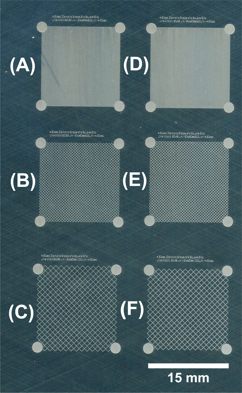 | ||
| Fig. 2 Zoomed view of grid engravings on the standard DLC surface image captured using epson perfection V500 photo scanner (model J251A, SN: K5ZW215808). Grid (A)–(C) has of 20 μm lines at 200 μm, 500 μm and 1000 μm spacing respectively. Grid, (D)–(F) has 30 μm lines at 200 μm, 500 μm and 1000 μm spacing respectively. | ||
2.2. Characteristics of chrome and standard DLC
Gravure printing surfaces are truly engineered surfaces that rely on control of surface characteristics to obtain desired print performance. The properties of the surface that influence contact phenomena when the surface comes into contact with another solid medium (i.e. metal doctor blade, paper, or plastic) are mechanical properties such as hardness, and tribological properties such as friction and wear. Contact phenomena occur when the surface comes into contact with a fluid (i.e. ink in gravure printing). Physical properties such as surface energy contribute to wetting and adhesion.45Fig. 3 shows the contact angles (CAs) of test liquids and surface free energy (SFE) on gravure surfaces. It is observed that the contact angle of diiodo-methane is similar, whereas the CA of water on chrome is 80° which is far higher than 51.2° for standard DLC. Higher contact angle values show that the surface is more hydrophobic which may result in air entrapment and insufficient ink filling in the image engravings during ink doctoring.9 However, CA measurements of standard DLC-coated surface show that it is not too hydrophobic and may result in lower air entrapment, good ink filling, and sufficient release properties.49 SFE disperse values are similar for both surfaces, due to the similar contact angle readings for diiodo-methane. The SFE polar value for standard DLC-coated surface is four times higher than the chrome-coated surface value. Overall, the SFE data indicate that standard DLC-coated surface has a higher SFE than chrome-coated surface. Fig. S-3 and S-4 (ESI†) shows the images test liquids CA on chrome and standard DLC surface.
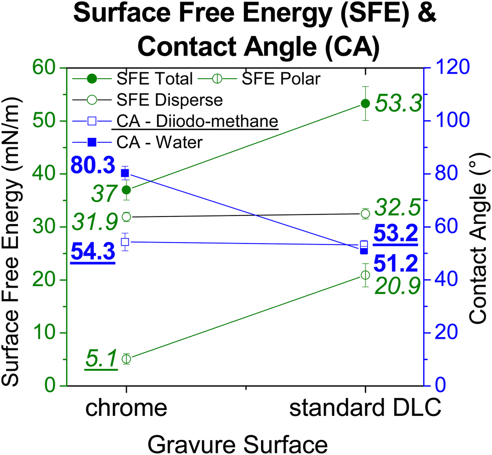 | ||
| Fig. 3 Double Y-axis graph showing surface properties of gravure surface: the Y-axis on the left shows surface free energy (SFE) numerical values in mN m−1 in green and the Y-axis on the right shows contact angle (CA) numerical values in degrees with blue. The X-axis represents two types of gravure surface: chrome and standard DLC. | ||
Names of the 3D parameter filter tools that used an analyzer algorithm in vision 64 software to evaluate the OPDx file that has 3D surface data of the plain portion of chrome and standard DLC layers may be found in Table S-1 of the ESI,† and the cited ref. 50. The gray scale images and 3D contour color plots of both the surfaces are provided in Fig. S-1 and S-2 of the ESI.†
Surface metrology data of the gravure surfaces are shown in Table 2. The S parameter hybrid values Sdr and Sdq, measured on the standard DLC-coated surface, display lower readings that those on chrome-coated surfaces. In addition, the Sa, Sq, Sz, and Rz parameter readings of the standard DLC-coated surfaces are notably lower than chrome-coated surfaces. These data suggest that the low surface roughness of standard-DLC may contribute to uniform ink doctoring and transfer to the substrate in image areas.
| Surface name | S parameters – hybrid | S parameters – height | R z analysis | |||
|---|---|---|---|---|---|---|
| S dq (avg RMS slope in degree) | S dr (avg developed interfacial area ratio) | S a (avg roughness in nm) | S q (avg RMS roughness in nm) | S z (avg peak to valley in nm) | R z in nm | |
| Standard DLC | 0.41 | 0.003 | 16.20 | 20.55 | 593.20 | 431.41 |
| Chrome | 0.83 | 0.017 | 32.56 | 41.91 | 743.38 | 611.27 |
 | ||
| Fig. 4 The R (reference) and M (measurement) cursors were positioned on the contour plot of the OPDx file. (A) Measured distance between R and M is given by ΔX, (B) height difference between R and M is given by ΔZ. | ||
Fig. 5 shows a graph of the average measured width and depth of 20 μm and 30 μm line engravings (sample size = 7) for each of the 1000 μm, 500 μm and 200 μm spacings on the gravure surfaces. It is observed from the figure that the widths and depths of the engravings on the chrome and standard DLC surfaces have negligible differences.
 | ||
| Fig. 5 Graph of the measured (sample size = 7) average width and depth of on the 20 μm and the 30 μm line grid engravings for each of 1000 μm, 500 μm, and 200 μm spacings. | ||
2.3. Ink and substrate characteristics
In order to pair ink and substrate for use in the gravure printing process, the fluid properties of the ink and surface properties of the substrate must meet gravure printing guidelines to achieve successful print image reproduction. Here the engineered gravure printing surface is used on an RK Proofer, a tabletop flatbed gravure printing test lab instrument, to test the transfer of conductive ink from its surface to the substrate. The result of ink transfer is successful reproduction of fine-line electrodes on the substrate.There were two types of ink used in these experiments: (1) LOCTITE ECI 7007 E&C, manufactured and supplied by Henkel, in which carbon is used as a conductive filler and (2) versa HR Black 60 (no.: 1424868-3410), manufactured and supplied by INX, in which black 7 pigment is used as a conductive filler. Both inks have conductive particles of size of <1 micron. Hot air-drying treatment at a temperature of approximately 80 °C (±5 °C) for a duration of 5 to 7 seconds was used for curing both type of inks after printing. In the experimental results the names the inks are designated as ECI 7007 and black 60.
There were two types of substrates used in this experiment, and both were manufactured and supplied by Celanese Corporation, USA (DuPont Teijin Films). These substrates were (1) Melinex® ST339, which is a 300 gauge or 75 μm thick white film with acrylic adhesion primer on both the sides that has a surface roughness Ra = ∼350 nm, and (2) Melinex® ST506, which is a 500 gauge or 125 μm thick clear film with acrylic adhesion primer on both sides and a surface roughness Ra = ∼15 nm. In the experimental results the names of substrates are designated as white PET for Melinex® ST339 and clear PET for Melinex® ST506.
 | ||
| Fig. 6 Double Y-axis graph showing surface properties of substrates: the Y-axis on the left shows surface free energy (SFE) numerical values in mN m−1 in green and the Y-axis on the right shows contact angle (CA) numerical values in degrees in blue. The X-axis show two types of substrate surface: white PET (Melinex® ST339) and clear PET (Melinex® ST506). | ||
SFE data suggest that the SFE total values are similar for both substrates. The SFE polar value for clear PET is slightly lower than for white PET. Overall, the data indicate that white PET has a slightly higher total SFE value than that of clear PET. Examining the substrate specifications, the white PET has a surface roughness Ra = ∼350 nm while clear PET has a surface roughness Ra = ∼15 nm. This disparity in surface roughness could be a factor that leads to this marginal difference in the SFE of the substrate. Nonetheless, this slight difference would not likely affect the printability on the surfaces since they are both coated with an acrylic adhesion primer.
Viscosity measures the behavior of two layers of substances in generating friction within a fluid. This friction between the substances determines the flow resistance of a fluid. The resistance to flow of a fluid is measured in centipoise (cp) or milli Pascal seconds (mPa s).
An AMETEK DV-1 viscometer, type LV (model: DV1MLVTJ0, SN: 86044067) was used to measure the viscosity reading. The viscometer uses the LV-02 (#62) spindle and a supporting guard attached for stable viscosity measurement. The rotational speed of the spindle on the viscometer is then set to 50 RPM, and the viscosity on the viscometer display is noted. The same procedure is repeated at 100 RPM. The viscosity measurements of ink are shown in Fig. 7. The viscosity of ECI 7007 was higher than that of black 60. Both inks had different formulations using different types of conductive carbon. The viscosity of these inks was not reduced for the experiments to ensure that the conductive functionality of the ink remained unaltered, thereby allowing for accurate comparison of fine line reproduction between chrome and standard DLC.
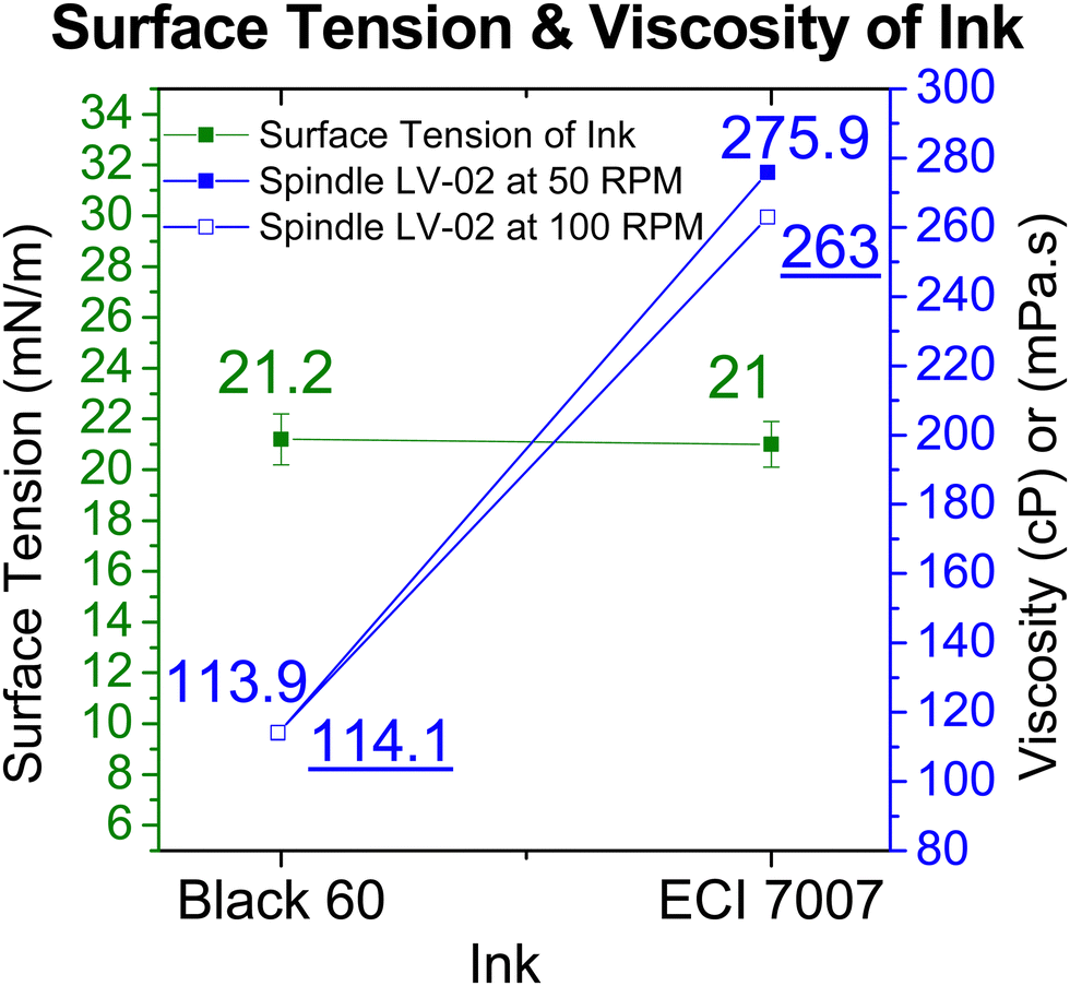 | ||
| Fig. 7 Double Y-axis graph showing surface properties of conductive carbon ink: the Y-axis on the left shows surface tension (ST) numerical values in mN m−1 in green and the Y-axis on the right shows viscosity numerical values in cP or mPa s in blue. The X-axis show two types of conductive carbon ink: black 60 and ECI 7007. | ||
The First Ten Angstroms FTÅ200 (SN: 022846) instrument with NAVITAR optics, an image sensor, and a 0.3 megapixel camera (point grey research FMVU-03MTM-CS, SN: 13494929) were connected to FTA32 Software V2.1 Build 381 to capture images of the shape of an ink drop. The pendant drop method was then used to identify the shape of the ink drop hanging from a needle, which was then used to calculate the surface tension of the liquid ink. A 10-mL BD syringe and dispensing needle from Jensen global were employed. A 20-gauge needle with a tip width of 0.914 mm was chosen for dispensing the necessary volume of conductive ink for pendant drop measurement. The sessile drop method was used to measure the contact angle of the ink on the substrate and gravure surface; a 30-gauge needle with a smaller tip width of 0.305 mm was chosen for dispensing a small volume of ink to ensure accurate sessile drop shape and contact angle measurements. The surface tension (ST) results are shown in Fig. 7. These results suggest that the surface tension of black 60 and ECI 7007 inks is similar. Pendant drop ST image of inks are shown in Fig. S-7 and S-8 of the ESI.† As shown in Fig. 8, the CA of black 60 is lower on white PET than on clear PET, so the ink will spread and wet the white PET more easily than the clear PET. The CA of ECI 7007 is only slightly different, indicating that the ink will wet the surfaces of both substrates similarly. However, the CA of both ink types on chrome and standard DLC are only slightly different, suggesting that they will fill the engraved lines with ink similarly. However, with the standard DLC-coated surface, higher SFE may allow for easier ink filling and the good tribological properties of DLC may allow for good ink release from the engravings for transfer to the PET substrates. Sessile drop CA images of inks on PET surfaces are shown in Fig. S-9 and S-12 (ESI†), and CA images of inks on the gravure surfaces are shown in Fig. S-13 and S-16 of the ESI.†
 | ||
| Fig. 8 Graph showing contact angle properties of conductive black 60 and ECI 7007 carbon ink. The Y-axis on the left shows contact angle (CA) numerical values in degrees. The X-axis shows substrate and gravure surfaces. | ||
The measured dry ink film thickness that was achieved on three types of Mayer rod drawdowns is presented in Fig. 9A. As these results show, rod 13 allows more conductive ink to pass through when compared to rod 10 and rod 7. Additionally, when more ink passes through rod 13, the black 60 ink spreads more easily on the white PET substrate, likely due to its lower viscosity. This results in a slightly lower ink film thickness compared to ECI 7007. The contact angle of the inks on clear PET is similar, and hence the ink spreading and leveling resulted in similar dry ink film thickness with rod 13.
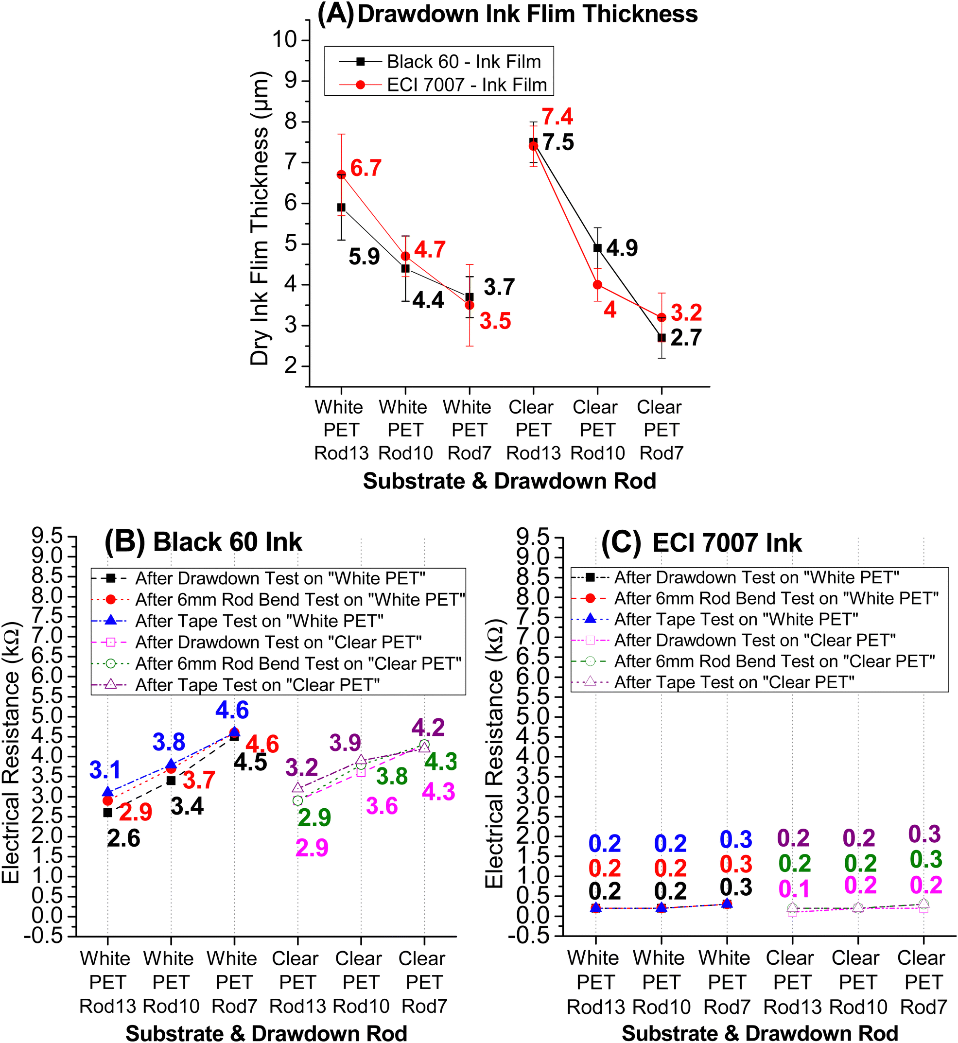 | ||
| Fig. 9 Ink drawdown characterization. (A) Dry ink film thickness of black 60 and ECI 7007 carbon ink drawdowns: Y-axis shows dry ink film thickness in micrometers and X-axis show substrate and used Mayer rod. The graph (B) black 60 ink and the graph (C) ECI 7007 Ink, shows the respective electrical resistance of ink drawdown on white PET and clear PET substrates measured at three stages: after drawdown test, after 6 mm rod bend test and after tape test when the ink is dry: Y-axis show the resistance numerical values in kilohms and X-axis show the PET substrate and used Mayer rod. Note: the rod number indicates the diameter (measured in mils) of the steel wire wound on them. Rod no. 7, 10 and 13 represents diameter of the wire, which is 7 mils (177.8 μm), 10 mils (254 μm) and 13 mils (330.2 μm) respectively. Finer the wire, the smaller the groove space formed by adjoining wires on the Mayer rod. | ||
The cylindrical mandrel or pencil bend tests were conducted to evaluate the resistance of a conductive ink coating to cracking and detachment from the base substrate.55 With the dried ink on the surface, the substrate was uniformly bent around a cylindrical mandrel or pencil for two to three seconds at 180 degrees. After bending, the conductive ink coating was inspected for cracking. This test demonstrates the flexibility of the conductive ink film and its resistance to cracking at a given bending radius. In this experiment, a 6 mm stainless steel cylindrical rod/mandrel was used to assess the crack resistance of the ink drawdown on a flexible PET substrate. After the mandrel bend test, the electrical resistance of the ink drawdown was measured.
The electrical resistance of conductive carbon inks before and after undergoing a bend and tape test is presented in Fig. 9B and C for black 60 and ECI 7007 inks respectively. As shown here, the black 60 ink has a higher electrical resistance than ECI 7007. Additionally, the electrical resistance of each of the inks decreases with an increasing rod number, indicating that more ink deposited on the substrates leads to a lower electrical resistance as expected. After the tape test, no lifting or detachment of the ink was observed on both substrates. No cracking of the ink was visible when the drawdown was inspected after the tape and bend tests. Moreover, minimal increase in the electrical resistance is observed after the tape test, suggesting that both ink types have good adhesion to the two types of substrates. Minimal variation in the electrical resistance measurements was detected after the mandrel bend test on the drawdown, indicating that both inks possess excellent bendability and crack resistance.
2.4. Doctor blade material
There were two type of wiping doctor blades used in the experiments: (1) “White-Carbon Steel with Lamella Tip,” a metal doctor blade (0.006 inches (0.150 mm) thick and 0.750 inches in height) manufactured and supplied by the Daetwyler Company USA and (2) “E600 0.6 mm double laminate with step Lamella Tip” plastic doctor blade manufactured and supplied by Esterlam Ltd, UK. A metal blade and a plastic blade were used in the experiments because the influence of blade materials on the print performance is unknown and not reported in the literature. It is interesting to determine how blade material one being hard metal (carbon steel doctor blades have a hardness of 550 HV) and other being plastic affect the print performance of chrome- and standard DLC-coated surfaces. If there a difference, then this could help inform future research or lead to subsequent studies.2.5. Printing using gravure RK proofer
The K printing proofer (SL: 124383, year 2022 from RK Print Coat Instruments Ltd in the UK), a bench top laboratory scale gravure printing instrument, was used in the experiment. The K proofer has a flat horizontal bed on which either a chrome or standard DLC-fabricated gravure flat plate is clamped. It also has a doctor blade holder assembly with a blade holder and precision screw gauge to adjust the blade-to-plate pressure mechanically. A metal doctor blade is fixed to the holder at an angle of 55 degrees relative to the flat surface of the gravure plate. An EPDM (ethylene propylene diene monomer) rubber at 65 shore hardness was used as an impression roller in the assembly and is attached with a precision screw gauge to adjust the rubber roller-to-plate pressure mechanically. The device has a speed control knob to increase and decrease the print speed from 1 to 10 meters s−1. The parameters of the K-proofer are adjusted to simulate the gravure printing process. Unlike the roll-to-roll gravure printing, the image carrier in the form of a ballard shell/skin must be peeled and flattened for use on the K-proofer. During printing, the recessed cells in the image pattern are filled with ink and then wiped clean from the non-image areas with a metal doctor blade. As the surface of the gravure plate is flat, and the printing speed is slower, the viscosity of the ink needs to be higher. The substrate must be attached to the impression roller in a cut-sheet form. The ink is transferred from the ink-filled cells of the patterned image to the substrate at the nip (the point at which the impression roller presses the substrate against the ink-filled cells of the flat gravure surface) during the impression roller forward motion. Before applying the ink and after printing, the flat gravure plate was cleaned thoroughly to ensure the line grids were free of dirt and dry ink particles. Lastly, the ink was thoroughly mixed with a propeller mixer to ensure its homogeneity before it was used in the experiment.Eight print trials were conducted using the K printing proofer. The trials used different print conditions such as blade, ink, and substrate for both chrome and standard DLC surfaces. The conditions that were used in each trial are listed in Table 3. The print speed was 6 meters s−1 for all trials. Each print trial condition began with chrome surface, and then chrome was replaced with standard DLC to repeat the trial under the same print condition.
| Trial no. | Experiment name | Print conditions | ||
|---|---|---|---|---|
| Blade type | Ink type | Substrate type | ||
| T1 | Trial one print experiment | Metal | Black60 | White PET |
| T2 | Trial two print experiment | Metal | Black60 | Clear PET |
| T3 | Trial three print experiment | Metal | ECI7007 | White PET |
| T4 | Trial four print experiment | Metal | ECI7007 | Clear PET |
| T5 | Trial five print experiment | Plastic | Black60 | White PET |
| T6 | Trial six print experiment | Plastic | Black60 | Clear PET |
| T7 | Trial seven print experiment | Plastic | ECI7007 | White PET |
| T8 | Trial eight print experiment | Plastic | ECI7007 | Clear PET |
For each printing trial, several samples were obtained by performing the printing process in batches. The process of transferring the conductive ink from the gravure surface to the substrate consisted of five steps: (1) attaching the substrate to the impression roller, (2) dispensing 1–2 mL of ink near the doctor blade, (3) printing the substrate at a speed of 6 meters s−1, (4) removing the printed substrate for drying, and (5) cleaning the ink from the gravure plate and blade with n-propyl acetate.
There were two type of wiping doctor blades used in the experiments: (1) “White-Carbon Steel with Lamella Tip,” a metal doctor blade (0.006 inches (0.150 mm) thick and 0.750 inches in height) manufactured and supplied by the Daetwyler Company USA and (2) “E600 0.6 mm double laminate with step Lamella Tip” plastic doctor blade manufactured and supplied by Esterlam Ltd, UK. The conductive ink LOCTITE ECI 7007 E&C manufactured and supplied by Henkel is referred to as ECI7007, and versa HR black 60 (no.: 1424868-3410) manufactured and supplied by INX is referred to as black 60 in the experiment. Further, the PET substrates Melinex® ST339, a 300 gauge or 75 μm thick white film, is referred to as white PET, and Melinex® ST506, a 500 gauge or 125 μm thick super clear film, is referred to as clear PET in the experiment.
2.6. Line width, electrical resistance, transparency data generation
In this experiment, a PIAS-II (SN: 2232120060763) digital microscope with visible optics HR, height resolution of ∼5 μm (SN: 2210020060763) and visible optics LR, low resolution of ∼37 μm per pixel (SN: 2213020060763) from QEA (quality engineering associates, Inc. USA) were used in measuring the printed line width in μm on PET substrates.56 The PIAS-II device and respective visible optics have been calibrated and verified to a known line width using the calibrated verification target (SN: 2240020060242). The PIAS-II is used to measure line width as per ISO-13660.57,58 After measuring the line width from the printed samples, statistical analysis is used to determine which gravure surface performed better. The electrical resistance of the printed conductive fine lines of the grid patterns was measured using the sinometer VC9808, a digital multimeter (SN: 091756725) that is connected with pointed test probes and test leads. Further, grid transparency was measured using a spectrophotometer device, the Barbieri spectro LPF qb (SN: C0060243), with an 8 mm aperture opening. Here grid transparency is given by L* value which refers to the relative amount of light that is allowed to pass through a given grid pattern. Transparency measurements allow evaluation of the effect of line width gain in grid line spacing to quantify how much more or less light passes through the grid.3. Results and discussions
The Results section includes line width, electrical resistance and transparency of the printed electrode grid samples obtained from eight trial experiments that used standard DLC and chrome as gravure surface. Additionally, the statistical analysis of the line width data is presented.3.1. Line width and line width gain
In this section the results of the electrode line widths data, measured from the printed samples that are obtained in the experiments, are discussed in relation to the printing conditions. Digital microscopes, a c-mount PAXcam 3 (model: PX3-CM, SN: 16110051), digital camera mounted on a microscope connected to PAX-it 2 (v1.7.3.0) software is used to capture a 3 MP image at full resolution of 2048 × 1536 to aid in reporting and for visual display of printed fine lines from DLC surface and chrome. Microscopic images of the prints obtained in various trial print experiments and print conditions are found in the ESI.† The reference figure numbers associated to trial experiments and print conditions are given in the Table 4.| Trial no. | Experiment name | Print conditions | Reference figure in ESI | ||
|---|---|---|---|---|---|
| Blade type | Ink type | Substrate type | |||
| T1 | Trial one print experiment | Metal | Black 60 | White PET | Fig. S-17 and S-18, ESI |
| T2 | Trial two print experiment | Metal | Black 60 | Clear PET | Fig. S-19 and S-20, ESI |
| T3 | Trial three print experiment | Metal | ECI7007 | White PET | Fig. S-21 and S-22, ESI |
| T4 | Trial four print experiment | Metal | ECI7007 | Clear PET | Fig. S-23 and S-24, ESI |
| T5 | Trial five print experiment | Plastic | Black 60 | White PET | Fig. S-25 and S-26, ESI |
| T6 | Trial six print experiment | Plastic | Black 60 | Clear PET | Fig. S-27 and S-28, ESI |
| T7 | Trial seven print experiment | Plastic | ECI7007 | White PET | Fig. S-29 and S-30, ESI |
| T8 | Trial eight print experiment | Plastic | ECI7007 | Clear PET | Fig. S-31 and S-32, ESI |
Graphs in Fig. 10 and 11 illustrate line width and gain from 20 μm and 30 μm grids in chrome and standard DLC print samples across trials T1 to T8. Fig. 10A–C depict measured 20 μm lines, and Fig. 11A–C show 30 μm lines. Additionally, Fig. 10D and 11D display line width gain for 20 μm and 30 μm lines, respectively, across all trials. Line width gain was measured by subtracting the nominal line width from the average of the measured line widths of 25 samples. Then the width gain was divided by the nominal line width and multiplied by 100 to determine the line width gain as a percentage.
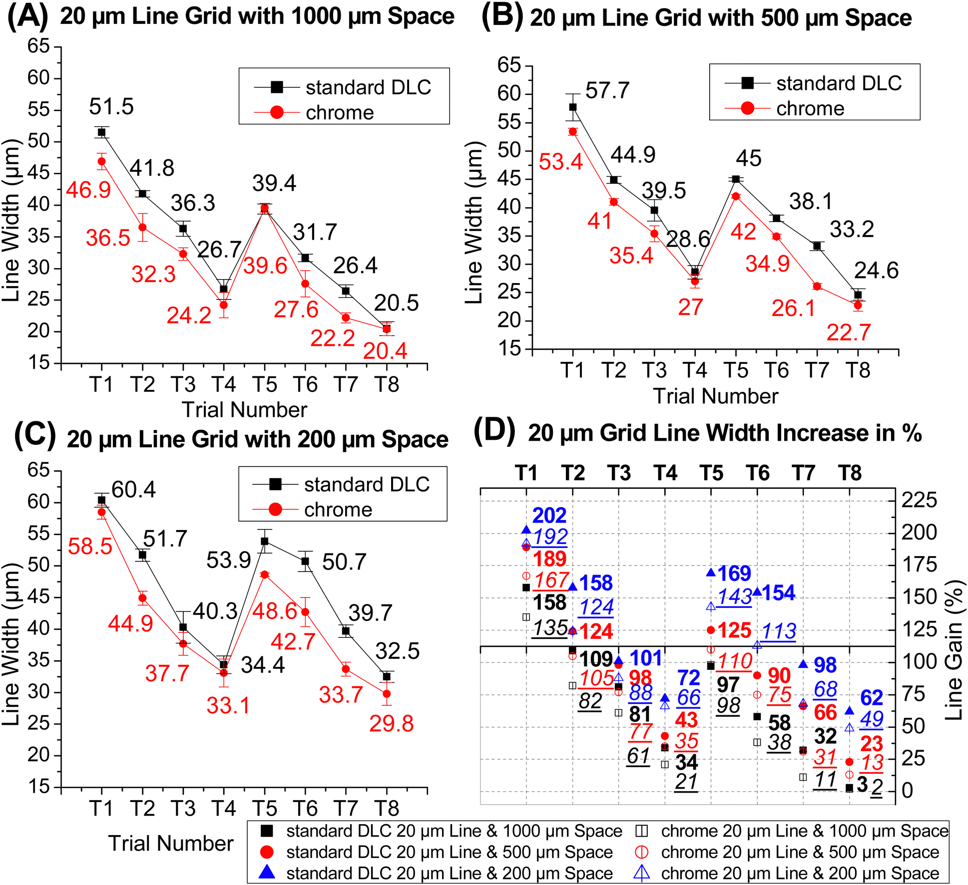 | ||
| Fig. 10 Line width (μm) and line width increase (%). The graph (A)–(C) illustrates measured line width (average of 25 data points) and graph (D) illustrates percentage increase in line width from each 20 μm grids at their 1000 μm, 500 μm, and 200 μm spacing in print samples obtained from chrome and standard DLC in all the trials from T1 to T8. The Y-axis in (A)–(C) shows measured line width (μm) and Y-axis in (D) shows line width increase (%). X-Axis in all the graphs show trial T1 to T8 experiments. | ||
 | ||
| Fig. 11 Line width (μm) and line width increase (%). The graph (A)–(C) illustrates measured line width (average of 25 data points) and graph (D) illustrates percentage increase in line width from each 30 μm grids at their 1000 μm, 500 μm, and 200 μm spacing in print samples obtained from chrome and standard DLC in all the trials from T1 to T8. The Y-axis in (A)–(C) shows measured line width (μm) and Y-axis in (D) shows line width increase (%). X-Axis in all the graphs show trial T1 to T8 experiments. | ||
Analysis of line width and gain graphs in Fig. 10 and 11 indicates increased line width in 20 μm and 30 μm prints from standard DLC compared to chrome, with exceptions where the difference is negligible. Notably, line width trends consistently downward across trials T1 to T8 for both standard DLC and chrome prints, showcasing uniformity under varying print conditions. The line width in prints shows a downward trend from trial T1 to T4, and a similar trend is observed in trials T5 to T8.
Analyzing line width data in Fig. 10 and 11 for 20 μm and 30 μm in all trials, key observations emerge. Trials T1 and T5 used black 60 ink and white PET substrate, but T1 used a metal blade, while T5 used a plastic blade. The metal blade, harder and 0.150 mm thick, does not flex during ink doctoring, resulting in high ink shear and effective filling of line engravings. Conversely, the plastic blade, softer and 0.6 mm thick, may flex, leading to lower ink shear and less ink filling in line engravings. Plastic blades also require less pressure than steel. Ink filling and transfer depends on viscosity of ink and printing speed.26 Consequently, the line width in T5 is less than in T1, highlighting the influence of blade material on the printed line width. Quantifying the impact of metal and plastic blades, their interaction requires further investigation with appropriate instrumentation, but this study focuses on chrome and standard DLC.
Trials T2 and T6 use black 60 ink and clear PET substrate. T2 employed a metal blade, while T6 used a plastic blade. In T6, line width was smaller than T2, attributed to the blade type, consistent with discussions in T1 and T5 results. Line widths in T2 and T6 were lower than in T1 and T5. Despite similar total surface free energy (SFE) for white PET (43 mN m−1) compared to clear PET (41.7 mN m−1), clear PET's lower SFE polar component (5.9 mN m−1vs. 7.5 mN m−1) and higher contact angle (CA) with black 60 ink (59.7° vs. 48.1°) likely contributed to reduced line width. In T1, the metal blade and white PET-ink interaction increased line width, while in T2, metal blade influence persisted, but clear PET-ink interaction reduced line width.
Trials T3 and T7 used ECI 7007 ink and white PET substrate. T3 used a metal blade, while T7 used a plastic blade. In T7, the measured line width was smaller than in T3, indicating the doctor blade type as a contributing factor, as explained earlier in T1 and T5 result discussion. Trials T4 and T8 used ECI 7007 ink and clear PET substrate. T4 used a metal blade, while T8 used a plastic blade. In T8, the measured line width was smaller than in T4, with blade type as a contributing factor. Additionally, line widths in T4 and T8 were lower than in T3 and T7, indicating a downward trend influenced by the polar properties of the substrate, as explained earlier in results discussions comparing T2 and T6 with T1 and T5.
Comparing prints from trial groups T1, T5, T2, T6 with trial group T3, T7, T4, T8 reveals that the latter group has lower line width gain compared to the former. Notably, both trial groups use different inks—T1, T5, T2, T6 with black 60 ink, and T3, T7, T4, T8 with ECI 7007 ink. ECI 7007 ink exhibited higher viscosity at 262.95 cP, while black 60 ink had a measured viscosity of 114.07 cP. The higher viscosity of ECI 7007 may contribute to the observed line width differences between the trial groups. Various factors like rheology, shear thinning, ink composition, and additional properties (conductive particles, solvent, binder, additives) can influence line width, but this experiment focuses on trends in measurement data from standard DLC and chrome print samples.
This experiment doesn't delve into a detailed analysis of various print conditions. The primary focus is comparing line width trends between prints from chrome and standard DLC surfaces under the same trial conditions. Standard DLC prints consistently exhibit higher line width than chrome under these conditions. When comparing trial results, the line width trend in standard DLC aligns with that of chrome under different print conditions. The observed increase in line width for standard DLC prints, compared to chrome prints under identical conditions, suggests good surface wetting, ink doctoring, and ink release properties for standard DLC.
3.2. Electrical resistance and transparency of the printed grid
The grid line's electrical resistance is inversely proportional to the deposited ink and conductive particles. Increased ink deposition results in thicker lines with more conductive particles, leading to lower electrical resistance. In this experiment, resistance values indicate the amount of ink deposited. Lower resistance signifies more ink and conductive particles, while higher resistance indicates less ink and particles transferred from the gravure surface.Fig. 12 and 13 show electrical resistance in kiloohms for 20 μm and 30 μm grids at 1000 μm, 500 μm, and 200 μm spacings in print samples from chrome and standard DLC across trials T1 to T8. Fig. 12A–C display resistance in samples with 20 μm line grids at specified spacings, while Fig. 13A–C show resistance for 30 μm line grids. Fig. 12D and 13D illustrate the transparency of 20 μm and 30 μm line grids and associated spacings in all trials. Trial groups T1, T2, T5, T6 used black 60 conductive ink (viscosity 114.07 cP), while T3, T4, T7, T8 used ECI 7007 conductive ink with higher viscosity (262.95 cP).
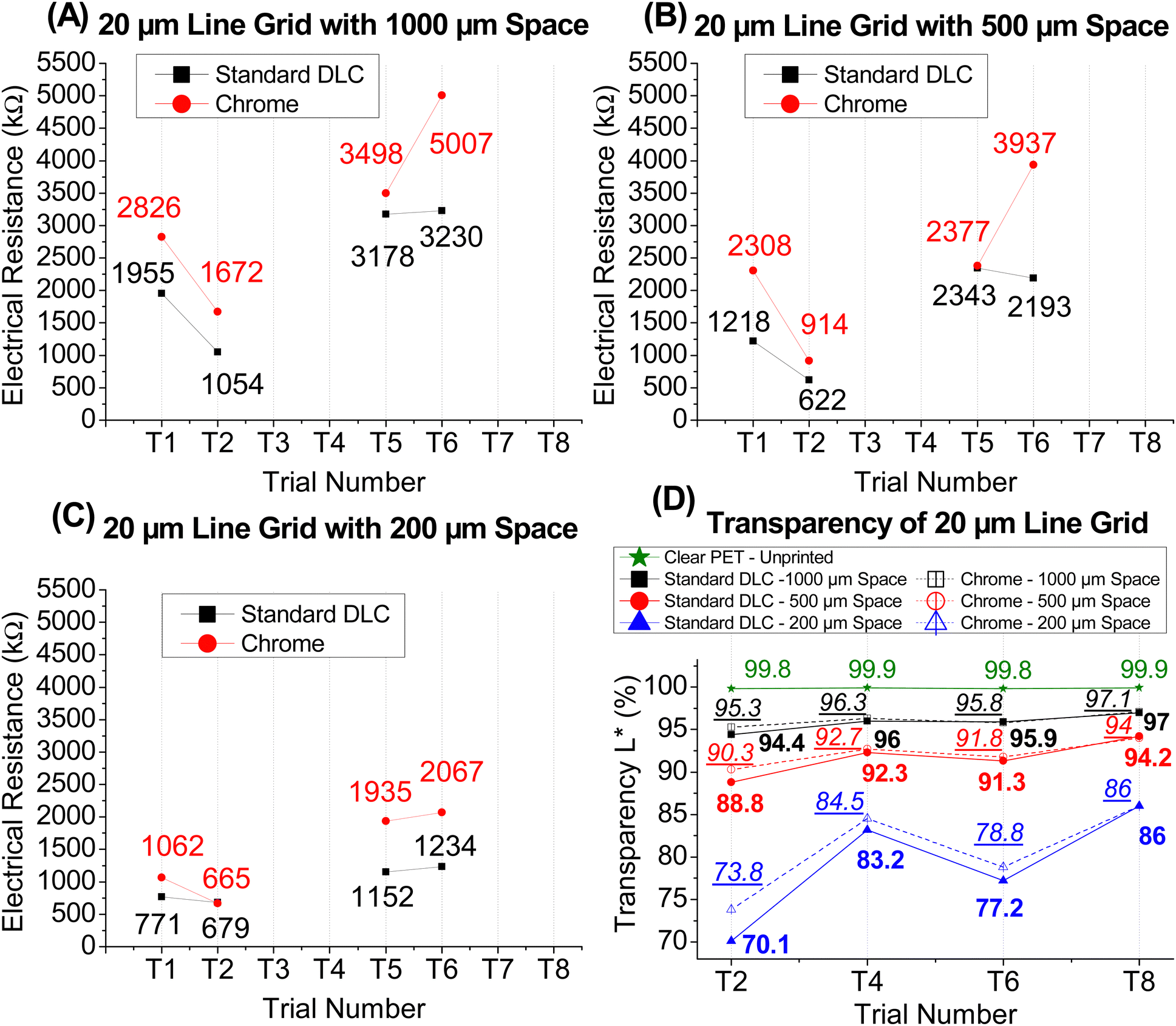 | ||
| Fig. 12 Electrical resistance (kΩ) and transparency L* (%). The graph (A)–(C) illustrates measured electrical resistance in kilohm (kΩ) that was measured from 20 μm grids at their 1000 μm, 500 μm, and 200 μm spacing in print samples obtained from chrome and standard DLC in all the trials from T1 to T8 experiments and graph (D) illustrates the transparency (L*) that was measured from 20 μm grids at their 1000 μm, 500 μm, and 200 μm spacing in print samples obtained from chrome and standard DLC in trial T2, T4, T6 and trial T8 experiments that used clear PET substrate. The Y-axis in graph (A)–(C) shows measured electrical resistance (kΩ) and Y-axis in (D) shows transparency L* (%). X-Axis in all the graphs show trial T1 to T8 experiments. Note: there was no electrical resistance reading on lines of 20 μm grids printed with ECI 7007 ink in trial T3 and T4. | ||
 | ||
| Fig. 13 Electrical resistance (kΩ) and transparency L* (%). The graph (A)–(C) illustrates measured electrical resistance in kilohm (kΩ) that was measured from 30 μm grids at their 1000 μm, 500 μm, and 200 μm spacing in print samples obtained from chrome and standard DLC in all the trials from T1 to T8 experiments, and graph (D) illustrates the transparency (L*) that was measured from 30 μm grids at their 1000 μm, 500 μm, and 200 μm spacing in print samples obtained from chrome and standard DLC in trial T2, T4, T6 and trial T8 experiments that used clear PET substrate. The Y-axis in graph (A)–(C) shows measured electrical resistance (kΩ) and Y-axis in (D) shows transparency L* (%). X-Axis in all the graphs show trial T1 to T8 experiments. | ||
Fig. 10 demonstrate that trial group T3, T4, T7, T8 (using ECI 7007 ink with viscosity 262.95 cP) and trial group T1, T2, T5, T6 (using black 60 ink with viscosity 114.07 cP) exhibit measurable 20 μm lines on both chrome and standard DLC. However, Fig. 12 shows that in trial group T3, T4, T7, T8, the prints of 20 μm lines lack sufficient conductive particles for a measurable resistance value. It is crucial to consider that ink viscosity, along with other properties such as rheology, shear thinning, ink recipe matrix, solvent, binder, and additives, may influence the number of conductive particles present in the filled 20 μm line engravings. Lack of conductive particles in the ink that is transfer onto the substrate results in the absence of a measurable resistance. In this experimental data, the focuses on electrical measurement trends in print samples of standard DLC and chrome. Observing trial group T1, T2, T5, T6 that used black 60 conductive ink, the 20 μm lines printed by both chrome and standard DLC had enough conductive particles in them to give a measurable resistance value. It can be observed that the standard DLC printed samples has lower electrical resistance value compared to chrome consistently in this group. This means that the filled ink in the standard DLC line engravings transferred more ink than chrome line engravings.
Fig. 13 shows that both chrome and standard DLC produced 30 μm lines with sufficient conductive particles, yielding measurable resistance values. Across all trials from T1 to T8, standard DLC printed samples consistently exhibited lower electrical resistance values than chrome for 30 μm grids. This suggests that the ink in the standard DLC line engravings transferred more effectively than in chrome, potentially contributing to the observed, lower resistance, increased line width in standard DLC compared to chrome.
The sustained high ink transfer capability of standard DLC compared to chrome is further evident in Fig. 12D and 13D. These graphs illustrate the transparency of 20 μm and 30 μm line grids printed in trial groups T2, T4, T6, T8, utilizing clear PET substrate. The control, clear PET – unprinted, displays approximately 100% transparency. Notably, the transparency of printed grids is slightly lower for standard DLC compared to chrome. Once again, the increased line width in standard DLC contributes to the reduced transparency. This increased line width is associated with the effective ink transfer capability of standard DLC line engravings.
3.3. Statistical analysis of line width
Statistical analysis of data from eight experimental trials was conducted using Minitab software v21.2. A two-sample test for variance was applied to each comparison to determine whether to assume equal or unequal variance, followed by a two-sample t-test at a 5% significance level.59 The hypothesis that standard DLC is better or similar to chrome was tested. The results of the tests are tabulated in Tables S-2 and S-3 found in the ESI.† The two-sample t-test results of the chrome grid to standard DLC printed grid comparison indicate that the line width measured on printed samples of standard DLC is higher than that of chrome, and is statistically significant with a p-value less than 0.005 in all cases, except for a few where the line width of the print samples obtained from both the standard DLC and chrome were the same. Moreover, the t-test results of all grids comparison were found to be statistically significant.The ANOVA results in Table S-4 (ESI†), indicate that the surface, blade, substrate, ink and grid factors all have a significant impact on the line width, as the p-value is less than 0.005 for these factors. In this experiment blade, substrate, ink factors are used as print condition to assess the trend of ink release and line reproduction capabilities of standard DLC when compared to chrome.
4. Conclusion
This experiment marks the first instance in which printing conditions, including doctor blade, substrate and ink were included to assess their behavior with the chrome and standard DLC fabricated gravure surface in terms of achieving reliable line print reproduction. This study has demonstrated the potential for the standard DLC layer in reproducing fine line grids of 20 μm and 30 μm when compared to the chrome layer on flat gravure printing surfaces used in laboratory scale experiments. Upon examining the polar and dispersion components of the SFE total in the standard DLC surfaces, it is evident that the contribution of SFE polar component influenced the total SFE total when compared to chrome. High SFE and polarity can improve surface wetting and facilitate easy liquid release. Further, the S parameter hybrid value, that is, Sdr and Sdq, measured on the standard DLC surface, display lower readings than measurements on chrome surface. These again contribute to good ink wetting in the image area, while the low surface roughness of the standard DLC helps in smooth ink doctoring, filling of ink in the line engravings. These factors are one of the contributing in higher printed line width gain on standard DLC surfaces when compared to chrome surfaces.Comparing the experimental data between trial to trial with same gravure surface, it is observed that the print conditions such as the higher total surface free energy (SFE) and its polar component of the PET (polyethylene terephthalate) substrate, viscosity, and contact angle of the ink, doctor blade material and various other factors influenced the ink transfer behavior on the substrate. However, under different trial printing conditions, the chrome-printed samples displayed a noticeable trend in terms of line width, electrical resistance and transparency. Interestingly, standard DLC-printed samples also displayed the similar trend as chrome with the exception that it has good surface wetting, ink doctoring on the surface and good ink transfer capability from line engravings resulting line gain and low electrical resistance compared to chrome. The line width gain indicates that the DLC surface facilitates the ink to flow through the narrow spaces of the line engravings and cells, resulting in improved ink transfer onto the substrate under different printing conditions.
In drawing conclusions of the experimental data, the standard DLC surface show marginally more ink transfer onto the substrate during the printing process. It is important to note that the engraving line width and depth were similar on both surfaces. While these results suggest that standard DLC may serve as an excellent surface for reproduction of fine line grid structures when compared to chrome, these results focus on the print conditions and line width print performance characteristics captured on a small-scale laboratory printing device. It would be interesting to use the DLC surface in printing complex line structures and solid patterns on PET substrate using a scaleup roll-to-roll production machine to fully understand reproduction capacities at various print speeds. Further, the influence of blade material on reproduction of line and line width difference may require additional detailed analysis to quantitatively assess the blade and surface interactions and amount of ink deposited on the substrate using appropriate instruments. Further, using standard DLC cylinders on a roll-to-roll gravure printing process would be interesting future experimental study. In continuous roll-to-roll gravure printing process, as the printing cylinder rotates within the ink pan, the centrifugal force comes into play. This force pushes the ink outward, causing it to spread evenly across the surface of the cylinder before being controlled by the doctoring action of metal blade. The continuous riding contact between the metal blade tip and the roll gravure cylinder surface during ink doctoring ensures constant shear and induces shear thinning in the viscous ink. Consequently, ECI 7007 ink or other type of materials such as copper, silver, nano particle inks may better fill 20 μm line engravings and transfer ink to the substrate compared to the flat-surfaced gravure printing method. Future experiments will explore the roll-to-roll gravure cylinder printing method with different conductive inks. In the field of printed electronics, there are wide variety of conductive materials that are deposited to different extents on the surface in order to achieve the desired functionality in electronic components.
Further, analysis of the grid lines printed using standard DLC is statistically different from chrome and experimental data are real and repeatable. Ultimately, these data suggest that DLC can be one of potential viable surface for printing functional electrode structures for use in electronics and energy storage applications. Also, the environmentally friendly qualities of standard DLC make it possible to use and recycle materials responsibly in order to promote a more sustainable initiative in the electronics and energy storage industry.
Data availability
The data supporting this article have been included as part of the ESI.†Author contributions
All authors contributed equally.Conflicts of interest
There are no conflicts to declare.Acknowledgements
The authors would like to thank Think Laboratory Co., Ltd. Japan, INX International Ink Company, USA, Daetwyler USA, Esterlam Ltd, UK, Celanese Corporation, USA (DuPont Teijin Films) and Henkel Printed Electronics, The Netherlands for providing required materials for the experimental. We thank Dr. Harvey Levenson for his thoughtful contributions in our work and critical review of our paper. Further, this research was done under the guidance of late Dr. Paul D. Fleming III. This article is dedicated to Dr. Fleming's memory.References
- L. Engisch, Information on the use of Chromium Trioxide. https://swg-online.de/media/InfoCr-VIeng.pdf (accessed 2023-01-08).
- European Union. Printing Industry. https://ec.europa.eu/environment/archives/air/stationary/solvents/activities/pdf/89_en.pdf (accessed 2023-01-08).
- Gravure: Process and Technology, Gravure Education Foundation & Gravure Association of America, Rochester NY, 2003 Search PubMed.
- J. Siever, Gravure Printing in Europe – Status and Trends, Gravure Global, 2021, 62–63 Search PubMed (accessed 2023-03-04).
- A. S. Dahiya, D. Shakthivel, Y. Kumaresan, A. Zumeit, A. Christou and R. Dahiya, High-Performance Printed Electronics Based on Inorganic Semiconducting Nano to Chip Scale Structures, Nano Convergence, 2020, 7(1), 33, DOI:10.1186/s40580-020-00243-6.
- A. M. Tiara, H. Moon, G. Cho and J. Lee, Fully Roll-to-Roll Gravure Printed Electronics: Challenges and the Way to Integrating Logic Gates, Jpn. J. Appl. Phys., 2022, 61(SE), SE0802, DOI:10.35848/1347-4065/ac575e.
- G. F. M. N. Grau, Gravure-Printed Electronics: Devices, Technology Development and Design, PhD Dissertation, UC Berkeley, 2016. https://escholarship.org/uc/item/1bn3t372 (accessed 2023-03-18).
- R. Kitsomboonloha, Modeling and Applications of Highly-Scaled Gravure Printing, UC Berkeley, 2015. https://www2.eecs.berkeley.edu/Pubs/TechRpts/2015/EECS-2015-213.pdf (accessed 2023-03-18).
- J. Cen, R. Kitsomboonloha and V. Subramanian, Cell Filling in Gravure Printing for Printed Electronics, Langmuir, 2014, 30(45), 13716–13726, DOI:10.1021/la503180a.
- E. Hrehorova, M. Rebros, A. Pekarovicova and P. D. Fleming, Suitability of Gravure Printing for High Volume Fabrication of Electronics, Proceedings of Digital Fabrication, Pittsburgh, 2008, pp. 7–12 Search PubMed.
- H. K. Kang, Gravure-Printed Highly-Scaled Organic Thin-Film Transistors for Low-Cost and Large-Area Electronics, PhD Dissertation, UC Berkeley, 2013. https://escholarship.org/uc/item/0dd3n8b3 (accessed 2023-03-18).
- M. Bariya, Z. Shahpar, H. Park, J. Sun, Y. Jung, W. Gao, H. Y. Y. Nyein, T. S. Liaw, L.-C. Tai, Q. P. Ngo, M. Chao, Y. Zhao, M. Hettick, G. Cho and A. Javey, Roll-to-Roll Gravure Printed Electrochemical Sensors for Wearable and Medical Devices, ACS Nano, 2018, 12(7), 6978–6987, DOI:10.1021/acsnano.8b02505.
- A. de la Fuente Vornbrock, Roll Printed Electronics: Development and Scaling of Gravure Printing Techniques, PhD Dissertation, UC Berkeley, 2009. https://escholarship.org/uc/item/3tz7x1kn (accessed 2023-03-18).
- W. J. Scheideler, Scalable, Gravure-Printed Transparent Electronics: Materials and Process Design for Metal Oxide Thin-Film Transistors, PhD Dissertation, UC Berkeley, 2017. https://escholarship.org/uc/item/6kj4n0js (accessed 2023-03-18).
- D. Sung, A. de la Fuente Vornbrock and V. Subramanian, Scaling and Optimization of Gravure-Printed Silver Nanoparticle Lines for Printed Electronics, IEEE Trans. Compon. Packag. Technol., 2010, 33(1), 105–114, DOI:10.1109/TCAPT.2009.2021464.
- Gravure Printing. Research and Markets. https://www.researchandmarkets.com/reports/5302336/gravure-printing-global-strategic-business (accessed 2023-07-11).
- Market Research. Global Gravure Printing Market. https://www.marketresearch.com/Global-Industry-Analysts-v1039/Gravure-Printing-32504111/(accessed 2023-01-08).
- P. Nandi, Packaging Printing Market. Research and Markets. https://www.marketresearchfuture.com/reports/packaging-printing-market-2119 (accessed 2023-07-11).
- The Business Research Company, Flexible Electronics Global Market Report; Flexible Electronics Market Size, Trends and Global Forecast To 2032, 2023. https://www.thebusinessresearchcompany.com/report/flexible-electronics-global-market-report (accessed 2023-03-18).
- S. Shintaro and S. Yoshinobu, Gravure Cylinder and Manufacturing Method Thereof. WO2016167115A1, 2016. https://patents.google.com/patent/WO2016167115A1/en (accessed 2023-01-08) Search PubMed.
- European Chemicals Agency. https://echa.europa.eu/-/chromium-trioxide-widely-used-in-plating-and-surface-treatment (accessed 2023-02-05).
- European Commission Decisions, 2020. https://eur-lex.europa.eu/legal-content/EN/TXT/?uri=uriserv%3AOJ.C_.2020.447.01.0005.01.ENG&toc=OJ%3AC%3A2020%3A447%3ATOC#ntr1-C_2020447EN.01000501-E0001 (accessed 2023-02-05).
- D. Geert, European Chemicals Agency, 2010. https://echa.europa.eu/documents/10162/6b11ec66-9d90-400a-a61a-90de9a0fd8b1 (accessed 2023-02-07).
- CARB. CARB passes new amendments to phase out toxic hexavalent chromium. https://ww2.arb.ca.gov/news/carb-passes-new-amendments-phase-out-toxic-hexavalent-chromium (accessed 2023-07-11).
- C. Seetharamiahsrinivasaraju, R. Shetty, S. Sood, D. K. Cohen, P. Sharma, H. Levenson, P. D. I. Fleming and J. R. Springstead, Sustainable and Eco-Friendly DLC Fabrication for Replacing Chrome on a Gravure Cylinder Surface, Langmuir, 2024, 40(6), 2849–2861, DOI:10.1021/acs.langmuir.3c02177.
- P. Kopola, M. Tuomikoski, R. Suhonen and A. Maaninen, Gravure Printed Organic Light Emitting Diodes for Lighting Applications, Thin Solid Films, 2009, 517(19), 5757–5762, DOI:10.1016/j.tsf.2009.03.209.
- J. M. Ding, A. de la Fuente Vornbrock, C. Ting and V. Subramanian, Patternable Polymer Bulk Heterojunction Photovoltaic Cells on Plastic by Rotogravure Printing, Sol. Energy Mater. Sol. Cells, 2009, 93(4), 459–464, DOI:10.1016/j.solmat.2008.12.003.
- Y. Choi, G. H. Kim, W. H. Jeong, H. J. Kim, B. D. Chin and J.-W. Yu, Characteristics of Gravure Printed InGaZnO Thin Films as an Active Channel Layer in Thin Film Transistors, Thin Solid Films, 2010, 518(22), 6249–6252, DOI:10.1016/j.tsf.2010.04.006.
- M. Montanino, G. Sico, A. De Girolamo Del Mauro, J. Asenbauer, J. R. Binder, D. Bresser and S. Passerini, Gravure-Printed Conversion/Alloying Anodes for Lithium-Ion Batteries, Energy Technol., 2021, 9(9), 2100315, DOI:10.1002/ente.202100315.
- G. L. Goh, S. Agarwala and W. Y. Yeong, High Resolution Aerosol Jet Printing of Conductive Ink for Stretchable Electronics, Proceedings of the 3rd International Conference on Progress in Additive Manufacturing (Pro-AM 2018), 2018, pp. 109–114 DOI:10.25341/D4FS3W.
- K. Nomura, H. Ushijima, R. Mitsui, S. Takahashi and S. Nakajima, Screen-Offset Printing for Fine Conductive Patterns, Microelectron. Eng., 2014, 123, 58–61, DOI:10.1016/j.mee.2014.05.009.
- G. L. Goh, H. Zhang, T. H. Chong and W. Y. Yeong, 3D Printing of Multilayered and Multimaterial Electronics: A Review, Adv. Electron. Mater., 2021, 7(10), 2100445, DOI:10.1002/aelm.202100445.
- C. H. Rao, K. Avinash, B. K. S. V. L. Varaprasad and S. Goel, A Review on Printed Electronics with Digital 3D Printing: Fabrication Techniques, Materials, Challenges and Future Opportunities, J. Electron. Mater., 2022, 51(6), 2747–2765, DOI:10.1007/s11664-022-09579-7.
- C. H. Kim, H.-I. You and S.-H. Lee, Register Control of Roll-to-Roll Gravure-Offset Printing Equipment Considering Time Difference between Measurement and Actuation, Proc. Inst. Mech. Eng., Part C, 2012, 226(11), 2726–2738, DOI:10.1177/0954406211433247.
- K.-H. Shin, H. A. D. Nguyen, J. Park, D. Shin and D. Lee, Roll-to-Roll Gravure Printing of Thick-Film Silver Electrode Micropatterns for Flexible Printed Circuit Board, J. Coat. Technol. Res., 2017, 14(1), 95–106, DOI:10.1007/s11998-016-9844-y.
- H. A. D. Nguyen, C. Lee and K.-H. Shin, Approach to Optimizing Printed Conductive Lines in High-Resolution Roll-to-Roll Gravure Printing, Robot. Comput.-Integr. Manuf., 2017, 46, 122–129, DOI:10.1016/j.rcim.2017.01.003.
- M. K. Välimäki, E. Jansson, V. J. J. Von Morgen, M. Ylikunnari, K.-L. Väisänen, P. Ontero, M. Kehusmaa, P. Korhonen and T. M. Kraft, Accuracy Control for Roll and Sheet Processed Printed Electronics on Flexible Plastic Substrates, Int. J. Adv. Manuf. Technol., 2022, 119(9–10), 6255–6273, DOI:10.1007/s00170-022-08717-z.
- J.-H. Noh, I. Kim, S. H. Park, J. Jo, D. S. Kim and T.-M. Lee, A Study on the Enhancement of Printing Location Accuracy in a Roll-to-Roll Gravure Offset Printing System, Int. J. Adv. Manuf. Technol., 2013, 68(5), 1147–1153, DOI:10.1007/s00170-013-4907-z.
- M. Pudas, J. Hagberg and S. Leppävuori, Printing Parameters and Ink Components Affecting Ultra-Fine-Line Gravure-Offset Printing for Electronics Applications, J. Eur. Ceram. Soc., 2004, 24(10), 2943–2950, DOI:10.1016/j.jeurceramsoc.2003.11.011.
- S. Khan, L. Lorenzelli and R. S. Dahiya, Technologies for Printing Sensors and Electronics Over Large Flexible Substrates: A Review, IEEE Sens. J., 2015, 15(6), 3164–3185, DOI:10.1109/JSEN.2014.2375203.
- P.-C. Yu, C.-C. Hong and T.-M. Liou, Bendable Transparent Conductive Meshes Based on Multi-Layer Inkjet-Printed Silver Patterns, J. Micromech. Microeng., 2016, 26(3), 035012, DOI:10.1088/0960-1317/26/3/035012.
- S. Flege, R. Hatada, W. Ensinger and K. Baba, Improved Adhesion of DLC Films on Copper Substrates by Preimplantation, Surf. Coat. Technol., 2014, 256, 37–40, DOI:10.1016/j.surfcoat.2013.12.020.
- J. H. Kim, S. Kang, J.-W. Park, E.-D. Park, Y.-K. Jun, J. Y. Han, J. H. Jung, N. Kim and G.-H. Lee, Tailored Hydrogen-Free Carbon Films by Tuning the Sp2/Sp3 Configuration, ACS Appl. Electron. Mater., 2021, 3(4), 1771–1779, DOI:10.1021/acsaelm.1c00046.
- X. Rao, J. Yang, Z. Chen, Y. Yuan, Q. Chen, X. Feng, L. Qin and Y. Zhang, Tuning C–C Sp2/Sp3 Ratio of DLC Films in FCVA System for Biomedical Application, Bioact. Mater., 2020, 5(2), 192–200, DOI:10.1016/j.bioactmat.2020.02.009.
- A. A. G. Bruzzone, H. L. Costa, P. M. Lonardo and D. A. Lucca, Advances in Engineered Surfaces for Functional Performance, CIRP Ann., 2008, 57(2), 750–769, DOI:10.1016/j.cirp.2008.09.003.
- D. H. Kaelble, Dispersion-Polar Surface Tension Properties of Organic Solids, J. Adhes., 1970, 2(2), 66–81, DOI:10.1080/0021846708544582.
- D. K. Owens and R. C. Wendt, Estimation of the Surface Free Energy of Polymers, J. Appl. Polym. Sci., 1969, 13(8), 1741–1747, DOI:10.1002/app.1969.070130815.
- E. B. Gutoff and E. D. Cohen, 14 – Water- and Solvent-Based Coating Technology, in Multilayer Flexible Packaging, ed. J. R. Wagner, Plastics Design Library; William Andrew Publishing, 2nd edn, 2016, pp. 205–234 DOI:10.1016/B978-0-323-37100-1.00014-4.
- H. Zhang, A. Ramm, S. Lim, W. Xie, B. Y. Ahn, W. Xu, A. Mahajan, W. J. Suszynski, C. Kim, J. A. Lewis, C. D. Frisbie and L. F. Francis, Wettability Contrast Gravure Printing, Adv. Mater., 2015, 27(45), 7420–7425, DOI:10.1002/adma.201502639.
- D. Cohen, Surface Texture Parameters. https://michmet.com/wp-content/uploads/2022/06/Michigan_Metrology_Surface_Texture_Parameters_Glossary.pdf (accessed 2023-01-08).
- Z. Fu, 13 – Pigmented Ink Formulation, in Digital Printing of Textiles, ed. H. Ujiie, Woodhead Publishing Series in Textiles, Woodhead Publishing, 2006, pp. 218–232 DOI:10.1533/9781845691585.3.218.
- Chemistry and Technology of Water Based Inks, ed. P. Laden, Springer Netherlands, Dordrecht, 1996 DOI:10.1007/978-94-009-1547-3.
- G. V. Calder, F. C. Hansen and A. Parra, Quantifying the Tape Adhesion Test, in Adhesion Aspects of Polymeric Coatings, ed. K. L. Mittal, Springer US, Boston, MA, 1983, pp. 569–582 DOI:10.1007/978-1-4613-3658-7_33.
- M. Rezaee, L.-C. Tsai, M. I. Haider, A. Yazdi, E. Sanatizadeh and N. P. Salowitz, Quantitative Peel Test for Thin Films/Layers Based on a Coupled Parametric and Statistical Study, Sci. Rep., 2019, 9(1), 19805, DOI:10.1038/s41598-019-55355-9.
- M. A. Riheen, T. K. Saha and P. K. Sekhar, Inkjet Printing on PET Substrate, J. Electrochem. Soc., 2019, 166(9), B3036–B3039, DOI:10.1149/2.0091909jes.
- M.-K. Tse, PIAS-II. https://www.qea.com/upload/files/products/2007ICJ_PIAS-II_070613.pdf (accessed 2023-05-14).
- J. C. Briggs and M.-K. Tse, Objective Print Quality Analysis and The Portable Personal IAS® Image Analysis System, NIHON GAZO GAKKAISHI, J. Imaging Soc. Jpn., 2005, 44(6), 505–513, DOI:10.11370/isj.44.505.
- PIAS-II-Users-Guide-v.1.5. https://www.qea.com/wp-content/uploads/2017/05/PIAS-II-Users-Guide-v.1.5.pdf (accessed 2023-05-14).
- D. C. Montgomery, Applied Statistics and Probability for Engineers, Wiley, 5th edn, 2011 Search PubMed.
Footnote |
| † Electronic supplementary information (ESI) available. See DOI: https://doi.org/10.1039/d4ma00562g |
| This journal is © The Royal Society of Chemistry 2024 |