
 Open Access Article
 This Open Access Article is licensed under a
 Creative Commons Attribution 3.0 Unported Licence
Understanding the morphological evolution of anodic tantalum oxide nanostructures in acidic medium†
Biswaranjan D.
Mohapatra
 *a,
Kinga
Pawlik
a,
Izabela
Darowska
a,
Łukasz
Gondek
b,
Marcin
Pisarek
c and
Grzegorz D.
Sulka
*a
*a,
Kinga
Pawlik
a,
Izabela
Darowska
a,
Łukasz
Gondek
b,
Marcin
Pisarek
c and
Grzegorz D.
Sulka
*a
aDepartment of Physical Chemistry & Electrochemistry, Faculty of Chemistry, Jagiellonian University, Gronostajowa 2, Krakow 30-387, Poland. E-mail: biswaranjan.mohapatra@uj.edu.pl; sulka@chemia.uj.edu.pl
bFaculty of Physics and Applied Computer Science, AGH University of Krakow, Mickiewicza 30, Krakow 30-059, Poland
cLaboratory of Surface Analysis, Institute of Physical Chemistry, Polish Academy of Sciences, Kasprzaka 44/52, Warsaw 01-224, Poland
First published on 9th July 2024
Abstract
Nanostructures of tantalum oxide (Ta2O5) have been recognised as important and versatile materials in nanotechnology and medicinal science. However, the synthesis of shape- and size-controlled Ta2O5 nanostructures faces enormous challenges due to multi-step and expensive procedures. Over the past two decades, anodic oxidation or anodization of Ta has emerged as a facile top-down method for fabricating Ta2O5 nanostructures. Nevertheless, controlling the fabrication geometry, such as the thickness of the Ta2O5 oxide layer, and the conditions for regulating nanodimple/nanoporous/nanotube/nanorod structures remains difficult, particularly in acidic media. In the present work, we aim to understand the formation and growth mechanism of anodic Ta2O5 (ATO) nanostructures, and the conditions necessary for achieving the desired nanopatterns by adjusting various anodization parameters (i.e., anodization potential, time and HF![[thin space (1/6-em)]](https://www.rsc.org/images/entities/char_2009.gif) :H2O ratio in the electrolyte). By controlling the anodizing potential and HF:H2O ratio, we have successfully obtained ATO layers with thicknesses ranging from ∼1.25 to ∼10.7 μm. Self-organized Ta2O5 nanotubes with a diameter of ∼55 nm were fabricated under the applied potential of 30 V for 2 or 4 min. The concepts and conditions for formation of Ta2O5 nanorods and agglomeration of nanotubes are revealed in this study. Furthermore, we have elucidated the rate limiting steps of Ta2O5 growth by applying various growth models. The crystallization of amorphous ATO structures and formation of Ta4O and Ta2O5 phases were understood by temperature programmed X-ray diffraction (XRD) analyses. We anticipate that the results presented in this study will enhance the current understanding of the growth of other anodic oxide nanostructures as well.
:H2O ratio in the electrolyte). By controlling the anodizing potential and HF:H2O ratio, we have successfully obtained ATO layers with thicknesses ranging from ∼1.25 to ∼10.7 μm. Self-organized Ta2O5 nanotubes with a diameter of ∼55 nm were fabricated under the applied potential of 30 V for 2 or 4 min. The concepts and conditions for formation of Ta2O5 nanorods and agglomeration of nanotubes are revealed in this study. Furthermore, we have elucidated the rate limiting steps of Ta2O5 growth by applying various growth models. The crystallization of amorphous ATO structures and formation of Ta4O and Ta2O5 phases were understood by temperature programmed X-ray diffraction (XRD) analyses. We anticipate that the results presented in this study will enhance the current understanding of the growth of other anodic oxide nanostructures as well.
1. Introduction
The designing and structuring of nanomaterials based on transition metal oxides (TMOs) play a key role in the advancement of nanotechnology and materials science.1–3 Over the past few decades, numerous synthetic methods with remarkable achievements have been documented in controlling the shape, size and overall morphology of TMOs.1–3 However, the opportunity and scalability provided by anodic oxidation methods to grow self-organized TMO nanostructures over a metallic substrate are explicitly unique and advantageous when compared to many other synthetic routes.4,5 Specifically, the interest in designing nanoporous/nanotube structures of valve metal oxides of Ti, Al, W, and Ta has been growing considerably because of their extraordinary properties for various applications (e.g., photocatalysis, photoelectrochemical (PEC) water splitting, supercapacitors, Li-batteries, and corrosion resistance to biomaterials).5–10 In addition to their direct uses, nanoporous/nanotube structures have also been applied as template materials for the deposition and fabrication of secondary nanomaterials with more enhanced physicochemical properties.10–15 However, until now, the majority of research and development on designing anodic oxide nanostructures has focused on Al2O3 and TiO2.8,11,12,16,17 In the last 10–15 years, this technique of nanostructure preparation has been successfully extended to other valve metal oxides, including tantalum oxide (Ta2O5).10,18–24Anodic tantalum oxides (ATOs) with nanoporous/nanotube morphologies, or ATOs decorated with nanostructured metal oxides (NiO, Mn3O4, and Fe3O4),13–15 or their derived materials such as Ta3N5,25–28 TaON,29 and TaS230 have found many applications in various domains such as photocatalysis for dye degradation, photo-electrocatalytic water splitting, supercapacitors, corrosion protection, and biomedical applications. Specifically, in most of these studies, the 1D nanotube or 3D nanoporous morphology played a crucial role in describing their physical properties and activity.18–30 Therefore, continuous efforts were given to tune the thickness of the nanoporous ATO layer and/or to alter the length and pore size of the nanotube structures.
The selection of an appropriate combination of anodizing electrolyte and applied potential is crucial for realizing nanostructures of ATOs. In earlier studies from the 20th century, various concentrations of compounds or acids such as H2SO4, HCl, H3PO4, Na2SO4, NaBF4, citric acid, etc. were used as an oxidizing agent, and potentials ranging from 10 to 300 V were applied to produce ATO layers.9,10 These studies mostly indicated the formation of compact layered structures of ATOs. In the 21st century, numerous studies have suggested that nanopore/nanotube arrays of ATO can be fabricated by anodizing tantalum in HF or NH4F containing organic/inorganic/organic–inorganic mixed electrolytes.18–24,31–44 The presence of fluoride ions in the electrolyte is considered the key ingredient for the formation of nanoporous/nanotubular ATO layers. Recently, L. Fialho et al. synthesized a well-ordered porous structure of ATOs in NH4F-containing ethylene glycol (EG)-based electrolytes.23 It is demonstrated that at different concentrations of NH4F (1.2 and 2.4 wt%) in the electrolyte or with an increase in applied electric field (60 V), uniform nanopores could be generated on the surface layer. However, the precise role of NH4F in the formation of ATO layers was not clearly addressed in this study. In a pioneering work, C. A. Horwood et al. developed precise anodization methods to control the length of Ta2O5 nanotubes, i.e., by manipulating the concentration of HF and anodization time.39 It was demonstrated that the growth rate of ATO nanotubes could be slowed down by consecutive adjustment of HF concentration (0.2–1.1 M) in 16 M H2SO4 electrolyte and by applying a relatively shorter anodization time (2 s to 4 min) at 15 V. ATO nanotubes with lengths up to 50–1000 nm were produced in this study. Similarly, H. A. El-Sayed et al. demonstrated the formation of nano-dimple and nanotube structures of ATOs in a stirred mixture of concentrated HF and H2SO4.38 In this study, the stirring of electrolytes during anodization is also considered as an important condition to acquire a well patterned surface structure. J. E. Barton et al. and C. F. A. Alves et al. intensively studied the impact of anodization voltage and HF:H2O ratio (in H2SO4 + HF + H2O electrolyte) on the diameter of the ATO nanodimples and nanotubes, respectively.24,31 In the case of ATO nanodimples, it was observed that the diameter increases from ∼30 to ∼150 nm with an increase in the applied potential from 15 to 50 V. However, in the case of ATO nanotubes, under fixed conditions of anodization (i.e., 4 wt% H2O in H2SO4 and 30 V), a change in the concentration of HF (0–3.7 wt%) has a significant impact on the outer diameter of the nanotubes and a minimal impact on the inner diameter of the nanotubes. C. F. A. Alves et al. further demonstrated that the formation of ATO nanostructures depends not only on the capability of HF to dissolve anodic oxide nanostructures but also on the concentration of H2SO4 needed to achieve highly ordered nanostructures.31 It is predicted that a high concentration (∼90 vol%) of H2SO4 in the electrolyte may reduce the dissociation of HF, leading to a reduction in reactive F− species and consequently, a decrease in the dissolution rate of tantalum oxide. Moreover, a remarkable difference in the dissolution rate has been observed in electrolytes containing 90 and 70 vol% H2SO4. It should be noted that well-ordered nanopore ATO patterns were observed when the volumetric ratio between H2SO4 and HF in the electrolytes was controlled to 8:0.5, 8:0.25, and 9:0.5. Similarly, the thickness of the ATO films and the length of the nanotubes (NTs) strongly depend on the quantity of charge passed during Ta oxidation and the strength of the applied electric field.9,23 In most studies, an applied voltage of 10–100 V and a duration of up to 60 min are considered ideal for the nanopore or nanotube formation.
Apart from this, the effect of adding organic solvents, such as ethylene glycol (EG) or dimethyl sulfoxide (DMSO), to the electrolyte containing HF and H2SO4 has also been thoroughly investigated. N. K. Allam et al. observed ATO nanorods (diameter of ∼50 nm) when Ta was anodized in 48% HF + 98% H2SO4 (1:9 vol%) electrolyte containing 5 vol% of EG at 10–15 V.40 It is demonstrated that a thin layer of precipitate debris could block the openings of the ATO nanotubes, resulting in the appearance of rod like structures. Moreover, in some cases, the tops of the nanotubes/nanorods of the ATO layers appeared to be merged together and formed a bundle like structure, thus affecting the nanotube openings further. Nevertheless, all these studies demonstrate the difficulties and variability associated with the formation and stabilization of ATO structures. Therefore, we anticipate that more extensive investigations of Ta anodization in electrolytes containing H2SO4, HF, and H2O need to be performed to comprehensively understand how the anodization parameters influence the overall morphology and physical properties of ATOs.
In the present work, we studied the growth of thin ATO films by a one-step anodization process in an electrolyte containing H2SO4, H2O, and HF. The effects of parameters such as the composition of the electrolyte (HF:H2O ratio), anodization potential and time on the nano-structural morphology and thickness of the ATO films were selectively and collectively explored by maintaining one parameter constant while varying the others. The appropriate electrochemical conditions for the formation of nanoporous, nanotube, and agglomerated nanotube structures were discussed. Special attention was given to evaluating the impurity content in the ATO structures through energy dispersive X-ray (EDX) analysis. Additionally, the evolution of X-ray diffraction (XRD) patterns and crystalline phases of the nanotube ATO structures at different temperature stages (25–800 °C) was studied by using temperature programmed XRD in an air or argon atmosphere. Moreover, under controlled voltage conditions, the growth kinetics of ATO layers was comprehended using a high field model (HFM) and interface model (IFM).
2. Experimental section
Tantalum (Ta) foils with a thickness of 0.25 mm and 99.9% purity (Thermo Fischer) underwent degreasing by sonication in acetone, ethanol, and then with H2O. In order to minimize roughness and achieve a mirror finish surface, all the Ta foils (1 cm × 1 cm exposed area) were electrochemically polished in a solution containing HF (17.5 ml) + HNO3 (17.5 ml) + H2O (65 ml) by connecting Ta specimens to a DC power supply (ARRAY electronic, model no. 3646A) as the anode and a Pt mesh of size (4 cm × 3 cm) as the cathode. Polishing was carried out under static electrolytic conditions at 10 °C by applying 20 V for 10 min. Thereafter, the electropolished Ta samples were rinsed with distilled water and then used for the anodization experiments. The anodization experiments were performed in a two-electrode cell with Ta foil (1 cm × 1 cm) as the anode and Pt mesh (4 cm × 3 cm) as the cathode. The electrolyte was a stirred mixture of H2SO4 (98 wt%), HF (48 wt%), and H2O with different volumetric ratios (9:0.1:0.9, 9:0.2:0.8, 9:0.4:0.6, 9:0.6:0.4, and 9:0.8:0.2). The distance between the electrodes was maintained at ∼2 cm, and the temperature of the electrolyte was controlled at 23 ± 1 °C using a recirculating chiller/cooler. The anodization was carried out in a potentiostatic mode, where both electrodes were connected to a coupled system consisting of a DC power supply (ARRAY electronic, model no. 3646A) and a PICOTEST Digit Multimeter (model no. M3500A). A constant potential of 15, 30, 40, or 80 V was applied with varying time durations ranging from 1 to 60 min for the experiments. Following anodization, the Ta foils were rinsed multiple times with water to remove residual electrolyte ions. Subsequently, the ATO covered Ta foils were air-dried and stored in a sample vial for analysis.
The morphology of the ATO layers was examined using a Hitachi S 4700 field emission scanning electron microscope (FESEM) operated at 20 keV. The elemental composition of the samples was analysed by energy dispersive X-ray spectroscopy (EDX). Crystalline phases of the materials were identified and analysed using a temperature-programmed glancing angle X-ray diffractometer (Anton Paar HTK1200N high-temperature oven, mounted in a Malvern Panalytical Empyrean diffractometer) over a temperature range of 25–800 °C. The measurement protocol included a temperature ramp of 10 °C min−1 to reach the desired temperature, followed by a 10 min waiting period for temperature stabilization, and a 70 min acquisition time for a single scan. The samples stage position was automatically calibrated for temperature expansion, and XRD measurements were conducted in either air or argon flow.
X-ray photoelectron spectroscopy (XPS) measurements were performed using a Microlab350 spectrometer at an energy of 1486.6 eV (Al-anode) and X-ray gun power of 20 W. Down peak deconvolution were performed using Thermo Avantage ver. 5.9911 by Thermo Fisher Scientific.
3. Results and discussion
3.1. Effect of anodization time and potential
Fig. 1a–f show SEM images of anodic tantalum oxide (ATO) layers grown at 15 V of Ta anodization in a solution comprising 90 ml H2SO4 (95 wt%) + 6 ml HF (40 wt%) + 4 ml H2O for durations ranging from 1 to 30 min. For the 1-minute ATO sample shown in Fig. 1a, no definite structure/nanostructure is observed, indicating insufficient anodization duration to produce a porous/tubular ATO layer. However, nanopatterns begin to emerge for samples treated under the same conditions for 2 min and beyond. SEM images of ATO samples prepared for 2 and 4 min reveal ordered nanoporous structures with approximately 30 nm of pore diameter (Fig. 1b and c). ATO layers prepared for 8, 15, and 30 min exhibit self-ordered nanotubular structures, with some parts covered by a thin layer of impurity material (Fig. 1d–f). The impurity layer seemed to block the openings of the pores. We suspect the layer may contain incorporated F and O from the electrolyte. The inset SEM images in Fig. 1a–f show the thickness of the ATO layers, indicating that it increases with anodization time, consistent with the findings of C. A. Horwood et al. and H. A. El-Sayed et al.38,39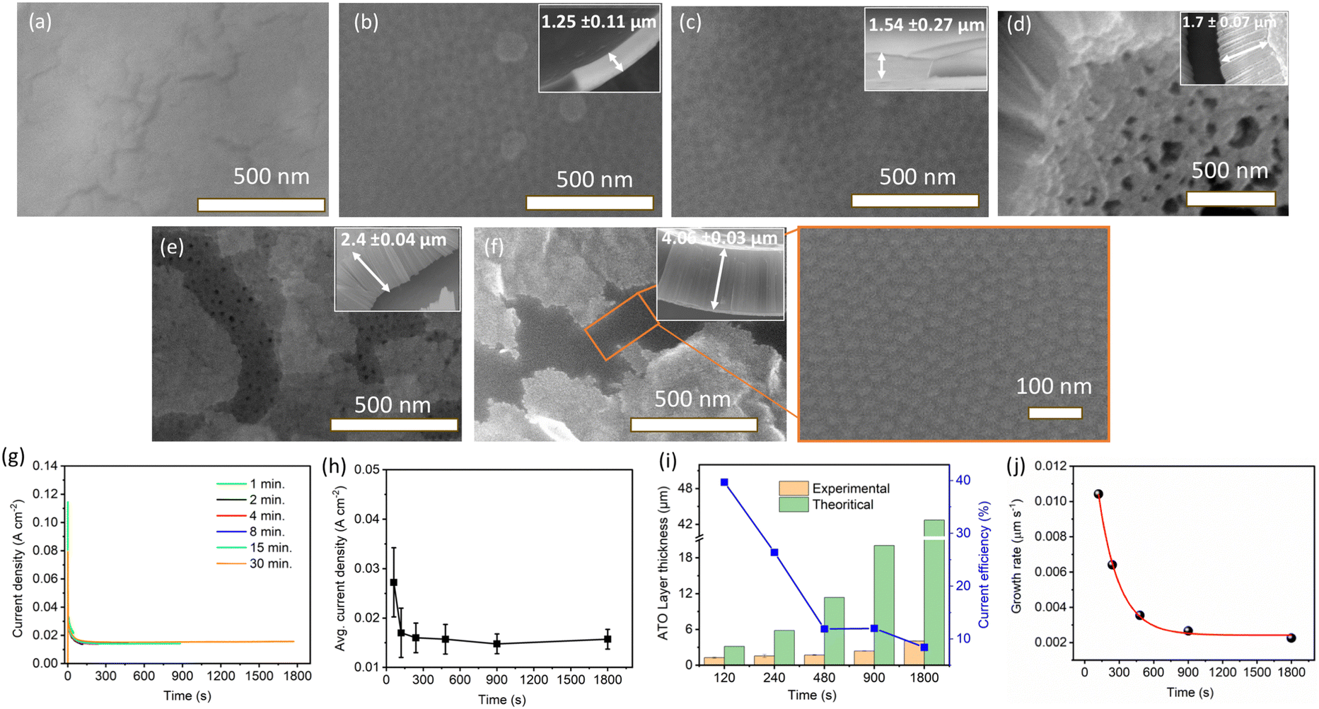 | ||
| Fig. 1 Top view SEM images of ATO layers prepared in a magnetically stirred electrolyte containing 90 ml H2SO4 (95 wt%) + 6 ml HF (40 wt%) + 4 ml H2O at 15 V and 23 °C, with an anodization time of (a) 1, (b) 2, (c) 4, (d) 8, (e) 15, and (f) 30 min. The insets show the corresponding cross-sectional SEM images of ATO layers. (g) Current density–time (i–t) curves for Ta anodization at 15 V with varying times. (h) Dependence of the steady-state current density on anodizing time at 15 V. (i) Comparison of experimental (SEM image) and theoretical thickness of the resulting ATO layers, along with current efficiency data (blue color). (j) Growth rate of ATO layers with respect to anodizing time at 15 V. | ||
Fig. 1g shows the current density-time curves for the anodization of Ta at 15 V with varying anodization times (1–30 min). As the voltage is kept constant at 15 V, the current densities follow a similar trend for all the cases, with a dramatic decrease observed within ∼120 s, attributed to the growth of a barrier-type oxide layer over the Ta substrate. Subsequently, the current density reaches a steady state value indicating a gradual growth of ATO layers. These current variations were previously correlated with different stages of compact (barrier) and nanoporous/nanotube ATO growth.44,45Fig. 1h illustrates the variation in average current density of Ta anodization with changing anodization time. The average current density for 1 min of Ta anodization (27.2 mA cm−2) is higher compared to 2 min (17 mA cm−2), and decreases to 16 mA cm−2 for 4 min. However, as predicted, minimal variation in the average current density (15–16 mA cm−2) is observed for longer anodization times (8, 15, and 30 min), indicating steady state current density values for longer anodization times.
In order to obtain further insight into ATO formation, the measured ATO thicknesses from the SEM images were compared with their theoretical values. The theoretical thickness of ATO layers was derived using eqn (1).46,47
 | (1) |
485 C mol−1), and ρOX is the density of amorphous Ta2O5 (8.2 g cm−3).46–48Fig. 1i shows the comparison of values between theoretical and experimental layer thicknesses formed at different anodizing times. Both the experimental and theoretical thicknesses of ATO layers increase with anodizing time up to 30 min. However, the theoretical thickness is observed to be much higher when compared to the corresponding experimental thickness. The current efficiency (CE) of the ATO formation can be deduced using the following equation:46,47 | (2) |
The SEM images of ATO layers obtained after 2, 4, 8, and 15 min of anodization at 30 V are presented in Fig. 2a–d, respectively. Clear images of self-organized nanotubular structures are observed for the ATO layers produced after 2 and 4 min, with the tube diameter of ∼55 nm (Fig. 2a and b). However, the top part of the self-organized nanotubular structures produced after 8 and 15 min appeared to be merged, resulting in blockages in the tube openings (Fig. 2c and d). This merging may have occurred due to the chemical etching of the triple contact points of nanotubes by fluoride ions and the ductile nature of the ATO nanotubes, causing them to bend and merge upon slight capillary forces occurring when samples dry after rinsing in water. Fig. 2e and f depict the anodization current density–time curves and average current density for anodization at 30 V with varying anodization times (2, 4, 8, and 15 min). The characteristic shape of the current density–time curve remains consistent across all time variations, gradually decreasing up to ∼200 s and then slowly stabilizing at a steady-state value. The average current density decreases with increasing anodization time, indicating a reduction in the growth rate of the ATO layer over time. The theoretical and experimental thicknesses of ATO layers formed at different anodizing times with a constant applied potential of 30 V, along with the corresponding current efficiencies, are summarized in Fig. 2g. For anodization durations of 2 and 4 min, the differences between experimental and theoretical thicknesses are negligible, with the current efficiency of ∼80%. However, for 8 and 15 min, significant differences between Lexp and Ltheo values are observed, accompanied by reduced current efficiency compared to 2 or 4 min. Fig. 2h shows a gradual decrease in the growth rate of ATO layers at 30 V with increasing anodization time. This observed anomaly in Lexp and Ltheo values and the decrease in growth rate with time can be attributed to the factors described earlier, i.e., (a) the chemical dissolution of the formed oxide layer by the fluoride ions, and (b) the occurrence of the water oxidation reaction during anodization, which may introduce errors in the calculation of theoretical layer thickness.46–51
 | ||
| Fig. 2 Top view SEM images of ATO layers prepared in a magnetically stirred electrolyte containing 90 ml H2SO4 (95 wt%) + 6 ml HF (40 wt%) + 4 ml H2O at 30 V, with an anodization time of (a) 2, (b) 4, (c) 8, and (d) 15 min. The insets show the corresponding cross-sectional SEM images of ATO layers. (e) Current density–time (i–t) curves for Ta anodization at 30 V with varying times. (f) Dependence of the steady-state current density on anodizing time at 30 V. (g) Comparison of experimental and theoretical thickness of the resulting ATO layers, along with current efficiency data (blue colour). (h) Growth rate of ATO layers with respect to anodizing time at 30 V. | ||
Fig. 3a–d show the top view of SEM images for ATO layers produced at 40 V for 2, 4, 8, and 15 min of anodizing time, respectively. A clear image of nanorods with a diameter ∼70 nm was observed for ATO produced after 2 min (Fig. 3a). As stated in the case of ATO structures produced at 15 V (durations of 8, 15, and 30 min), the top part of the nanotubes produced at 40 V (duration of 2 min) may have been covered with debris/impurities causing an appearance like nanorod structure. The formation of a debris/impurity layer may be explained as follows: the rapid etching process of Ta in the presence of fluoride ions releases Ta5+ into the electrolyte, which upon reacting with O2− would form tantalum oxide. This oxide is understood to be deposited/precipitated on the surface of the growing nanoporous/nanotube array rather than being incorporated within it.40 Another possible explanation could be the post-anodization treatment of anodic structures, which usually involves the removal of surface debris through ultrasonication in a suitable solvent medium (e.g., distilled water) for a few minutes. However, in the present case, the ATO nanostructures can easily detach from the metal substrate when rinsed in water, leading to a high probability of disturbing the regular arrangement of nanopores/nanotubes. Therefore, in order to retain the nano-structural arrangement and understand the effect of anodization conditions on the ATO thickness and pore size, the duration of rinsing was reduced to only a few seconds. This may result in the incomplete removal of the debris/impurity layer. The SEM image of ATO layers produced at 40 V for 4 min demonstrates a similar effect with some open pores in the nanotube structure (Fig. 3b). However, the nanotubes/nanorods of the top layer of 8- and 15-min ATO samples seemed to bend and merge together at discrete points (Fig. 3c and d). This again demonstrates how the capillary forces act on nanotubes/nanorods during drying.
 | ||
| Fig. 3 Top view SEM images of ATO layers prepared in a magnetically stirred electrolyte containing 90 ml H2SO4 (95 wt%) + 6 ml HF (40 wt%) + 4 ml H2O at 40 V, with anodization time of (a) 2, (b) 4, (c) 8, and (d) 15 min. The insets show the corresponding cross-sectional SEM images of ATO layers. (e) Current density–time (i–t) curves for Ta anodization at 40 V with varying anodizing times. (f) Dependence of the steady-state current density on anodizing time at 40 V. (g) Comparison of experimental and theoretical thickness of the resulting ATO layers, along with current efficiency data (blue color). (h) Growth rate of ATO layers with respect to anodizing time at 40 V. | ||
Moreover, we further investigate the bottom structure of the ATO nanotubes and the imprints of nanotube formation on the Ta foil. Fig. S1 (ESI†) shows the bottom layer of the ATO nanotubes produced at 40 V for 15 min. This showed a round-shaped closed ending of the nanotubes with a diameter of about 100 nm. It is to be noted that in all the cases, the ATO nanotube structures were not completely stable on the Ta foil and can be easily removed by rinsing with water. This process can leave behind the imprints of nanotube formation in terms of nanodimple morphology on the Ta foil (Fig. S2a, ESI†). Therefore, the freestanding ATO nanotubes can be seen discretely laying on Ta foil (Fig. S2b, ESI†). Fig. 3e and f show the current density–time curves and average current density of Ta anodization at 40 V with changes in anodization time (2, 4, 8, and 15 min). The characteristic shape of the fall in current density at 40 V with variation in time is observed to be the same when compared to 30 and 15 V, indicating a similar growth model at these potentials. The current densities decrease gradually up to ∼300 s and then slowly reach a steady-state value. This trend in the change of average current density values at 40 V is found to be similar to that of 30 V. The theoretical and experimental thicknesses of ATO layers formed at different anodizing times with a constant applied potential of 40 V and the corresponding current efficiencies are summarized in Fig. 3g. Both the theoretical and experimental thicknesses of ATO layers increase gradually with an extended anodizing time. Similar to the behavior observed for ATO layers formed at 30 V, the theoretical layer thickness at 40 V demonstrates a marked increase over time compared to the actual experimental results. Additionally, the current efficiency for all oxide layers formed at 40 V remains consistently below 50% (Fig. 3g). Fig. 3h illustrates a gradual decrement in the growth rate of ATO layers at 40 V as anodization time increases. The observed anomaly in Lexp and Ltheo values, as well as the decline in growth rate with prolonged anodization time, may mirror phenomena observed at 30 and 15 V, as detailed in the preceding section.
Furthermore, SEM images of ATO films produced at 80 V (anodizing time of 2 and 4 min) and 15 V (anodizing time of 6 h) were analyzed to understand the effect of higher anodizing potential and time. As shown in Fig. S3a and b (ESI†), the top view of the ATO films produced at 80 V for 2 and 4 min demonstrated irregularity in the arrangement of nanopores. Moreover, the average thickness (4.81 ± 0.13 μm) of the ATO films produced at 80 V (2 min) is close to the thickness (4.19 ± 0.23 μm) of ATO films formed at 40 V for the same anodizing time (Fig. S3c, ESI†). This similarity in the thickness of anodic layer may be due to breakdown events, evidenced by a continuous spark phenomenon occurring at 80 V. Therefore, anodization at 80 V imposed a detrimental effect on the ATO morphology. The ATO structures produced at a longer anodizing time (6 h) at 15 V showed the layer thickness (Lexpt) value of only 7.14 ± 0.12 μm (Fig. S4, ESI†). The Ltheo and current efficiency in this case were calculated to be 194.1 μm and 3.68%, respectively. These results clearly indicate a slower oxide growth rate compared to the etching process for a longer anodizing time (6 h).
In most of the studied potentials, a clear structure of nanopores/nanotubes was observed only for the 2- and/or 4-min anodization times. Therefore, the average pore diameters of the ATO nanopore/nanotubular structures were compared to investigate the effect of applied potential on the pore diameter at a constant anodizing time (4 min). Based on the evaluation of the SEM images, Fig. 4a–d shows the histogram for the distribution of pore diameter as a function of applied potentials (15, 30, 40, and 80 V). Fig. 4e demonstrates the dependence of the average pore diameter on the applied potentials. The average pore diameter increased from 31.94 nm at 15 V to 78.12 nm at 40 V and then decreased slightly to 70 nm at 80 V. The effect of anodization potential and time on the SEM-determined thickness of ATO layers is summarized in Fig. 5a. It can be observed that, at any constant time, the thickness of the ATO layer increases with an increase in anodization potential. The highest layer thickness of 10.7 μm is observed in the case of 40 V with 15 min of anodizing time. To further comprehend the kinetics of ATO growth, Ta foil (1 cm × 1 cm exposed area) was anodized for a consistent 6 h at 15, 30, and 40 V (Fig. 5b). The inset shows the anodic current density transients for the initial 60 seconds of the anodization process, revealing higher current density curves with elevated values corresponding to higher applied potentials.
 | ||
| Fig. 4 The pore diameter distribution for the ATO nanostructures produced at (a) 15 V, (b) 30 V, (c) 40 V, and (d) 80 V for 4 min in electrolyte containing 90 ml H2SO4 (95 wt%) + 6 ml HF (40 wt%) + 4 ml H2O. (e) Comparison of average pore diameter for ATO nanoporous/nanotube films produced at different anodizing voltages. | ||
 | ||
| Fig. 5 (a) Comparison of experimental thicknesses of ATO layers produced at 15, 30, and 40 V with varying anodizing times. (b) Current density–time (i–t) curves for Ta anodization carried out at 15, 30, and 40 V over a duration of 6 h in a magnetically stirred electrolyte containing (90 ml H2SO4 (95 wt%) + 6 ml HF (40 wt%) + 4 ml H2O) at 23 °C. The inset provides a broader view of the initial i vs. t stages of the anodization process. | ||
3.2. Rate determining step of the ATO growth
Previously, the kinetics of growth of anodic titanium oxide layers in electrolytes containing water, NH4F, and ethylene glycol was elucidated by applying various growth models such as the High Field Model (HFM) and Point Defect Model (PDM) known in some variants as the Interface Model (IFM).49,50 The HFM posits that the growth rate of the anodic film is limited by the migration of ionic species within the film under a high electric field, thereby identifying the rate-limiting step as a solid-state transport of ions through the oxide barrier layer.49–51 Whereas, the IFM hypothesizes that the rate-limiting step depends on the availability of ionic species at the oxide-electrolyte interface, i.e. the electric field-driven interface reaction. In the case of Ti anodization, it was demonstrated that the interface reaction is the rate limiting step for the growth of anodic titanium oxide. In the present case, the movement between the Ta–Ta2O5 (metal–metal oxide) interface may involve the transport of ions under the influence of the applied electric field, either by the transport of (i) Ta5+ in the direction of the electrolyte or (ii) OH−/O2− ions (and some other anions from the electrolyte) in the direction of metal. Under the high field approximation for some valve metals, the ionic current i is related to the anodization potential and the thickness of the barrier layer by the equation: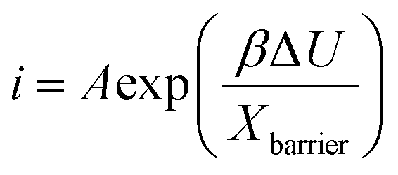 | (3) |
 | (4) |
 | (5) |
 | (6) |
Fig. 6a–c show the linear fitting of  vs. lni for the interface model at 15, 30, and 40 V respectively. All plots are derived from the initial time range of 30–300 s of the anodization data, as depicted in Fig. 5b. The square points represent the values of f (i,i′), while the red lines illustrate the linear fits to the data. For the IFM, where a potential-dependent interface reaction is thought to be the rate-determining step, a horizontal line is expected when f (i,i′) is plotted against lni. In our case we obtained straight lines with a positive slope, which suggests that the process of Ta oxidation under the studied experimental conditions is not consistent with the assumptions of the IFM model (slope = 0). Therefore, the rate-limiting step of the reaction is not the interface reaction, especially for the lowest anodizing potential. Since the slopes of the lines are getting smaller for higher potentials (they are getting closer to the horizontal line), the contribution of interfacial reactions in limiting the process rate is becoming more and more significant. Fig. 6d–f display the linear fitting of
  vs. lni for the high field model for 15, 30, and 40 V respectively. The black spheres represent the values of f (i − δ,i′), while the red lines indicate linear fits to the data. For all tested anodization potentials, positive slopes were observed on the curves, which indicates the high field model to be applicable. Previously, it has been observed that the slope values for f (i − δ,i′) vs. lni in the case of Ti anodization are much smaller at higher anodizing potentials compared to lower anodizing potentials.47 In our case, the slope value of 0.63 at 30 V is nearly 3 times smaller than 1.98 for 15 V. The slope value for 40 V (0.28) is nearly 2 times smaller than that for 30 V (0.63). This indicates an increase in the half jump distance (s) for ions at higher anodizing potentials, resulting in faster ionic transport, and consequently, the interfacial reaction could be more significant as the rate determining step in ATO growth in an electrolyte containing H2SO4, HF, and H2O.
 | ||
Fig. 6 The diagnostic plots of (a)–(c)  vs. lni and (d)–(f) vs. lni and (d)–(f)  vs. lni for potentiostatic anodization of Ta at 15, 30, and 40 V in electrolyte containing 90 ml H2SO4 (95 wt%) + 6 ml HF (40 wt%) + 4 ml H2O. The plots are sequentially ordered according to increased voltage. The current values were taken from Fig. 5b. vs. lni for potentiostatic anodization of Ta at 15, 30, and 40 V in electrolyte containing 90 ml H2SO4 (95 wt%) + 6 ml HF (40 wt%) + 4 ml H2O. The plots are sequentially ordered according to increased voltage. The current values were taken from Fig. 5b. | ||
3.3. Effect of the HF![[thin space (1/6-em)]](https://www.rsc.org/images/entities/h3_char_2009.gif) :H2O ratio in the electrolyte
:H2O ratio in the electrolyte
To investigate the influence of the HF to H2O ratio on the morphology and growth of ATO layers, the volumetric ratio between HF:H2O (1:9, 2:8, 4:6, 6:4, and 8:2) was varied in 100 ml of the electrolyte containing 90 ml of concentrated H2SO4. Fig. 7a illustrates the side view of the ATO layers produced at 15 V after 8 min of anodization, corresponding to different volumetric ratios of HF:H2O in the electrolyte. The ratios are provided for clarity in the top left corner of the SEM images. Remarkably, no ATO layers were observed in the case of Ta anodization in the electrolyte containing a 1:9 (v/v) HF:H2O ratio, suggesting unsuitable conditions for the ATO layer formation. However, for a 2:8 v/v ratio of HF:H2O, the thickness of the ATO layer was observed to be 3.22 ± 0.03 μm. Noticeable, the oxide thickness decreases as the HF:H2O ratio increases, reaching a minimum of 1.26 ± 0.06 μm for an 8:2 v/v ratio. Fig. 7c clearly illustrates the dependence of layer thickness on the HF:H2O ratio in the electrolyte. Fig. 7b shows the current density–time (i vs. t) curves obtained for different volume ratios (v/v) of HF:H2O in the electrolyte. From the graph, it is clear that electrolyte containing a higher ratio of HF:H2O leads to a higher anodizing current density. Therefore, theoretically, the thickness of the ATO layer should increase with an increase in the HF:H2O ratio. However, the reverse trend observed in the SEM results (Fig. 7c) may indicate a higher dissolution rate of ATO layers at higher concentrations of F− ions compared to the steady-state growth rates of oxides. Furthermore, the theoretical thicknesses of ATO layers formed at different volumetric ratios of HF:H2O in the electrolyte were calculated using eqn (1), and presented in Fig. 7d alongside the experimental thickness. This further supports the above findings. The current efficiency (CE) of the ATO formation in this case showed a decreasing trend with respect to an increase in the HF:H2O ratio (Fig. 7e). This decreasing trend in CE can be attributed to two major factors: (a) enhanced dissolution kinetics due to a high concentration of fluoride ions, which does not contribute to the anodization current, and (b) water oxidation reaction during the oxidation of Ta.
 | ||
| Fig. 7 (a) Cross-sectional SEM images and (b) current density–time curves recorded for Ta anodization at 15 V for 8 min in 100 ml electrolyte containing 90 ml H2SO4 (95 wt%) and varied HF:H2O v/v ratios (1:9, 2:8, 4:6, 6:4, and 8:2). (c) Average thickness of the ATO layers with respect to change in volumetric ratio of HF:H2O. (d) Comparison of theoretical and experimental thicknesses of ATO layers. (e) Current efficiency of ATO formation at 15 V for different volumetric ratios of HF:H2O in the electrolytes. | ||
3.4. Chemical and phase composition of ATO layers
The EDX spectra and EDX elemental mapping analyses were performed to acquire information about the elemental composition of ATO layers formed under different conditions. Fig. 8a–e show the EDX elemental mapping images of the self-organized ATO layer obtained at 30 V for 4 min. The mapping images illustrate that Ta and O are homogeneously distributed within the ATO layer. Additionally, some impurities (S and F) possibly originating from the electrolyte, were also found in the elemental mapping. This suggests that the F and S may have been incorporated into the ATO layers during anodization. These findings further corroborate observations made by M. M. Momeni et al. for anodic nanoporous ATO structures produced at 15 V in a 2.2 ml HF + 89.2 ml H2SO4 + 8.6 mL H2O electrolyte.21Fig. 8f displays the corresponding EDX spectrum of the ATO layer. The EDX spectrum and elemental mapping images for ATO layers formed at 40 V for 4 min and 15 V for 15 min exhibited similar results, with some amount of S and F detected in the ATO layer (Fig. S5 and S6, ESI†). The elemental composition of the ATO layers produced under these conditions is tabulated in Table 1. Notably, it was observed that the sulfur content in ATO-15 is higher compared to ATO-30 and ATO-40. A possible explanation for this may be associated with the post-treatment washing methods and the presence of an unwanted thin layer of debris/impurity, which could contribute to the increased S content in the EDX spectrum. | ||
| Fig. 8 Surface morphology (a) and EDX elemental mapping for (b) Ta, (c) O, (d) S, and (e) F for self-organized ATO nanotubes formed in the electrolyte containing 90 ml H2SO4 (95 wt%) + 6 ml HF (40 wt%) + 4 ml H2O at 30 V for 4 min. (f) Corresponding EDX spectrum. | ||
| Samples | Chemical composition (at%) | |||
|---|---|---|---|---|
| Ta | O | S | F | |
| ATO-15 | 54.21 | 29.61 | 12.14 | 2.35 |
| ATO-30 | 38.77 | 49.17 | 7.34 | 4.73 |
| ATO-40 | 43.95 | 45.74 | 6.43 | 3.88 |
To gain more accurate information on the surface composition and chemical environment of Ta, XPS measurements were performed for all the samples. Fig. 9a shows the XPS survey spectra for ATO-15, ATO-30, and ATO-40. The results of the XPS analysis further corroborate the EDX analysis and show the presence of impurities (F and S) in all samples. Notably, the peaks at about 169.5 and 685.8 eV correspond to S 2p and F 1s, respectively (Fig. 9a).23,52 The elemental atomic percentages of Ta, O, F, and S in the materials were calculated by integrating the respective areas under the XPS spectra and presented in Table S1 (ESI†). The stochiometric ratio between Ta and O was found to be 1:3.6, 1:3.5, and 1:45 for ATO-15, ATO-30, and ATO-40, respectively. This indicates the presence of oxygen defects in all ATO materials. Fig. 9b shows the deconvoluted Ta-4f XPS spectrum of ATO-30, which indicates the presence of six main components centered at 21.0 eV (metallic Ta0), 21.9 eV (Ta1+ from Ta2O), 26.5 eV (Ta5+ from Ta2O5), 27.5 eV (Ta–O in TaOx or Ta–F), 29.0 eV (Ta–F), and 30.0 eV (tantalate or organometallic compound).23,52 The deconvoluted Ta-4f spectra for ATO-15 and ATO-40 showed similar observations with the presence of Ta5+ and Ta1+ from the ATO structure and metallic Ta possibly from the cracks present in ATO layers (Fig. S7a and c, ESI†). The deconvoluted F 1s XPS spectra of ATO-30, ATO-15 and ATO-40 in Fig. 9c and Fig. S7b and d (ESI†) further indicate the incorporation of F− (F 1s, ∼686.0 eV) in the ATO structure.
 | ||
| Fig. 9 (a) XPS survey spectra for ATO-15, ATO-30, and ATO-40, (b) deconvoluted Ta 4f XPS spectra of thte ATO-30 sample, and (c) deconvoluted F 1s XPS spectra of the ATO-30 sample. | ||
The effect of annealing temperatures and atmosphere on the crystalline phase of the fabricated ATO nanotube structures were investigated using a temperature programmed X-ray diffraction (XRD) technique. The XRD spectrum of ATO structures produced at 30 V for 4 min was analysed at different stages of rising temperature under an air and argon atmosphere, respectively (Fig. 10a and b). For annealing under an air atmosphere, the ATO samples exhibited an amorphous nature up to 300 °C, with intense reflections from the (211) and (200) planes of the metallic Ta substrate at about 2θ = 69.5 and 55.5° (Fig. 10a). However, at about 350 °C, the samples showed XRD peaks at 2θ = 67.2° and 50° which correspond to the (411) and (400) planes of Ta4O (JCPDS card no. 03-065-6450). This may indicate the minimum temperature at which amorphous ATO converted to a crystalline phase. With a further increase in temperature up to 500 °C, a rise in reflection from (311) (2θ = 49°) and (111) planes (2θ = 36.4°) of Ta2O5 (JCPDS card no. 01-089-2834) was observed, with diminished reflection from the metallic Ta. This may indicate the beginning of the formation of the most thermodynamically stable phase of tantalum oxide. With a further rise in temperature up to 550 °C, new diffraction peaks appeared at about 2θ = 27.4 and 22.3°, corresponding to the (110) and (001) planes of Ta2O5, respectively. Interestingly, at this point, the diffraction intensity from the metallic Ta is significantly reduced, possibly due to oxidation of metallic Ta in an air atmosphere. Furthermore, the effect of an argon atmosphere on the crystalline phases of the fabricated ATO nanotube structures was investigated in a similar manner (Fig. 10b). In this case, the diffraction patterns at 2θ = 22.3, 27, 36.4, and 49° appeared at 700 °C and above, corresponding to the (001), (110), (111), and (311) planes of the Ta2O5 phase (JCPDS card no. 01-089-2834). Fig. S8 (ESI†) shows the temperature programmed XRD spectra under an air and argon atmosphere for ATO layers prepared at 40 V and 4 min. The observations in this case are quite similar to those of ATO formed at 30 V for 4 min. Hence, these results clearly indicate the amorphous nature of the freshly prepared ATO layers, and demonstrate that an early transition from the amorphous to the crystalline phase is possible when annealed in air.
 | ||
| Fig. 10 Temperature programmed XRD spectra under an (a) air and (b) argon atmosphere for ATO structures formed at the applied potential of 30 V for 4 min in the electrolyte containing 90 ml H2SO4 (95 wt%) + 6 ml of HF (40 wt%) + 4 ml H2O. | ||
4. Conclusions
Nanoporous, nanotube and nanorod morphologies of ATO films with thicknesses of a few μm were prepared in electrolytes containing H2SO4, HF and H2O. The dependence of nanostructural morphology on the anodizing potential, time, and electrolyte composition was analysed. Nanotubes with a diameter of ∼55 nm were formed after 2 and 4 min of anodization at 30 V. Prolonged anodizing time conditions (8 min and above at 15 V and 4 min and above at 30 and 40 V) resulted in the agglomeration of the top parts of the ATO nanotubes/nanorods. An increase in ATO thickness was observed with an increase in anodization time for all studied potentials (15, 30, and 40 V), and this relationship was found to be highly dependent on the volumetric ratio of HF:H2O in the electrolyte. A decreasing trend in ATO thickness with the increasing volumetric ratio of HF:H2O was ascertained. The growth rate of ATO, current efficiency, and the discrepancy between experimental and theoretical thicknesses were understood and explained in the context of the ATO dissolution rate and water oxidation reaction. The kinetics of ATO growth was explored by applying interface and high-field growth models, revealing that the HFM provides a better account of the experimental data compared to the PDM. However, the interface reactions occurring during ATO growth, particularly at higher potentials, were found to play a significant role in the rate limiting step. Physicochemical properties of ATO films were characterized using temperature programmed XRD, SEM, and EDX. Traces of impurities of S and F were found in all the nanoporous/nanotube structures. Thermal studies coupled with XRD showed the onset temperature (350 °C) for crystallization of amorphous ATO structures and the formation of the thermodynamically stable Ta2O5 phase at about 500 °C.
Author contributions
B. D. M. and G. D. S. designed the study, K. P., B. D. M. and I. D. performed the anodization experiments and collected the data. B. D. M., K. P. and G. D. S. analyzed the data. Ł. G. analyzed and interpreted the XRD data. M. P. analyzed and interpreted the XPS data. B. D. M. drafted the article. G. D. S. reviewed the data analysis, conceptualization, and the final version of the manuscript.Data availability
The data provided in this study are available at RODBUK Cracow Open Research Data Repository at https://doi.org/10.57903/UJ/8TZLXW.Conflicts of interest
There are no conflicts to declare.Acknowledgements
This research is part of the project No. 2021/43/P/ST5/02281 co-funded by the National Science Centre and the European Union Framework Programme for Research and Innovation Horizon 2020 under the Marie Sklodowska-Curie grant agreement no. 945339.References
- T. Guo, M. S. Yao, Y. H. Lin and C. W. Nana, CrystEngComm, 2015, 17, 3551–3585, 10.1039/C5CE00034C.
- G. Maduraiveeran, M. Sasidharan and W. Jin, Prog. Mater. Sci., 2019, 106, 100574, DOI:10.1016/j.pmatsci.2019.100574.
- S. Tajik, H. Beitollahi, Z. Dourandish, P. M. Jahani, I. Sheikhshoaie, M. B. Askari, P. Salarizadeh, F. G. Nejad, D. Kim, S. Y. Kim, R. S. Varma and M. Shokouhimehr, Electroanalysis, 2022, 34, 1065–1091, DOI:10.1002/elan.202100393.
- A. Huang, Y. He, Y. Zhou, Y. Zhou, Y. Yang, J. Zhang, L. Luo, Q. Mao, D. Hou and J. Yang, J. Mater. Sci., 2019, 54, 949–973, DOI:10.1007/s10853-018-2961-5.
- G. D. Sulka, Introduction to anodization of metals, in: Nanostructured Anodic Metal Oxides, ed. Sulka, G. D., Elsevier, 2020, pp. 1–34 DOI:10.1016/B978-0-12-816706-9.00001-7.
- J. Kapusta-Kołodziej, K. Syrek, A. Pawlik, M. Jarosz, O. Tynkevych and G. D. Sulka, Appl. Surf. Sci., 2017, 396, 1119–1129, DOI:10.1016/j.apsusc.2016.11.097.
- M. Zych, K. Syrek, M. Pisarek and G. D. Sulka, Electrochim. Acta, 2022, 411, 140061, DOI:10.1016/j.electacta.2022.140061.
- G. D. Sulka, Highly ordered anodic porous alumina formation by self-organised anodising and template-assisted fabrication of nanostructured materials, in Nanostructured Materials in Electrochemistry, ed. Ali Eftekhari, Wiley-VCH, 2008, pp. 1–116 DOI:10.1002/9783527621507.ch1.
- G. D. Sulka, Molecules, 2023, 28(10), 4040, DOI:10.3390/molecules28104040.
- N. L. S. Ngadiman, R. A. Rani, S. R. Makhsin, M. A. Ayub, D. Aryani and A. S. Zoolfakar, J. Mech. Eng., 2022, SI 11, 1–48, DOI:10.24191/jmeche.v11i1.23580.
- K. Syrek, M. Sołtys-Mróz, K. Pawlik, M. Gurgul and G. D. Sulka, Molecules, 2022, 21, 4789 CrossRef.
- M. Sołtys-Mróz, K. Syrek, Ł. Pięta, K. Malek and G. D. Sulka, Nanomaterials, 2022, 12, 1546 CrossRef.
- R. V. Gonçalves, H. Wender, P. Migowski, A. F. Feil, D. Eberhardt, J. Boita, S. Khan, G. Machado, J. Dupont and S. R. Teixeira, Phys. Chem. C, 2017, 121, 5855–5863, DOI:10.1021/acs.jpcc.6b10540.
- Y. Yang, Z. Peng, G. Wang, G. Ruan, X. Fan, L. Li, H. Fei, R. H. Hauge and J. M. Tour, ACS Nano, 2014, 8, 7279–7287, DOI:10.1021/nn502341x.
- A. Bordbar-Khiabani, S. Bahrampour, M. Mozafari and M. Gasik, Ceram. Int., 2022, 48, 3148–3156, DOI:10.1016/j.ceramint.2021.10.088.
- T. M. David, P. R. Dev, P. Wilson, P. Sagayaraj and T. Mathews, Electrochem. Sci. Adv., 2022, 2, e202100083, DOI:10.1002/elsa.202100083.
- D. Regonini, C. R. Bowen, A. Jaroenworaluck and R. Stevens, Mater. Sci. Eng., R, 2013, 74, 377–406, DOI:10.1016/j.mser.2013.10.001.
- R. V. Gonçalves, P. Migowski, H. Wender, D. Eberhardt, D. E. Weibel, F. C. Sonaglio, M. J. M. Zapata, J. Dupont, A. F. Feil and S. R. Teixeira, J. Phys. Chem. C, 2012, 116, 14022–14030, DOI:10.1021/jp303273q.
- R. V. Gonçalves, R. Wojcieszak, P. M. Uberman, S. R. Teixeira and L. M. Rossi, Phys. Chem. Chem. Phys., 2014, 16, 5755–5762, 10.1039/C3CP54887B.
- R. Kisslinger, S. Riddell, A. P. Manuel, K. M. Alam, A. P. Kalra, K. Cui and K. Shankar, ACS Appl. Mater. Interfaces, 2021, 13, 4340–4351, DOI:10.1021/acsami.0c18580.
- M. M. Momeni, M. Mirhosseini, M. Chavoshi and A. Hakimizade, J. Mater. Sci. Mater. Electron., 2016, 27, 3941–3947, DOI:10.1007/s10854-015-4246-y.
- M. M. Momeni, M. Mirhosseini and M. Chavoshi, Surf. Eng., 2017, 33, 83, DOI:10.1179/1743294415Y.0000000071.
- L. Fialho, C. F. A. Alves, L. S. Marques and S. Carvalho, Appl. Surf. Sci., 2020, 511, 145542, DOI:10.1016/j.apsusc.2020.145542.
- J. E. Barton, C. L. Stender, P. Li and T. W. Odom, J. Mater. Chem., 2009, 19, 4896–4898, 10.1039/B904964A.
- Y. Li, K. Nagato, J. Delaunay, J. Kubota and K. Domen, Nanotechnology, 2014, 25, 014013, DOI:10.1088/0957-4484/25/1/014013.
- Y. Li, T. Takata, D. Cha, K. Takanabe, T. Minegishi, J. Kubota and K. Domen, Adv. Mater., 2013, 25, 125–131, DOI:10.1002/adma.201202582.
- Z. Su, S. Grigorescu, L. Wang, K. Lee and P. Schmuki, Electrochem. Commun., 2015, 50, 15–19, DOI:10.1016/j.elecom.2014.10.017.
- S. Grigorescu, S. So, J. E. Yoo, A. Mazare, R. Hahn and P. Schmuki, Electrochim. Acta, 2015, 182, 803–808, DOI:10.1016/j.electacta.2015.09.159.
- S. Banerjee, S. K. Mohapatra and M. Misra, Chem. Commun., 2009, 7137–7139, 10.1039/B912549C.
- P. Li, C. L. Stender, E. Ringe, L. D. Marks and T. W. Odom, Small, 2010, 6, 1096–1099, DOI:10.1002/smll.201000226.
- C. F. A. Alves, S. Calderon V., P. J. Ferreira, L. Marques and S. Carvalho, Appl. Surf. Sci., 2020, 513, 1455752, DOI:10.1016/j.apsusc.2020.145575.
- E. Uslu, H. Öztatl, B. Garipcan and B. Ercan, J. Biomed. Mater. Res., 2020, 108, 2743–2753, DOI:10.1002/jbm.b.34604.
- M. A. A. Talip, R. A. Rani, R. A. Kadir, M. H. Mamat, M. F. A. Khalid, M. R. Mahmood and A. S. Zoolfakar, Int. J. Electrical Electronic Sys. Res., 2018, 13, 1 Search PubMed.
- S. Xia, J. Ni, S. V. Savilov and L. Li, Nano Energy, 2018, 45, 407–412, DOI:10.1016/j.nanoen.2018.01.026.
- R. S. Namur, K. M. Reyes and C. E. B. Marino, Mater. Res., 2015, 18, 91–97, DOI:10.1590/1516-1439.348714.
- W. Chen, Q. Tu, H. Wu, C. Zhao, X. Yao, W. Fan, S. Zhang, J. Ni and X. Zhang, Electrochim. Acta, 2017, 236, 140–153, DOI:10.1016/j.electacta.2017.03.024.
- K. Lee and P. Schmuki, Electrochem. Commun., 2011, 13, 542–545, DOI:10.1016/j.elecom.2011.03.005.
- H. A. El-Sayed, C. A. Horwood, A. D. Abhayawardhana and V. I. Birss, Nanoscale, 2013, 5, 1494–1498, 10.1039/c3nr33396e.
- C. A. Horwood, H. A. El-Sayed and V. I. Birss, Precise electrochemical prediction of short tantalum oxide nanotube length, Electrochim. Acta, 2014, 132, 91–97, DOI:10.1016/j.electacta.2014.03.128.
- N. K. Allam, X. J. Feng and C. A. Grimes, Chem. Mater., 2008, 20, 6477–6481, DOI:10.1021/cm801472y.
- W. Wei, J. M. Macak and P. Schmuki, Electrochem. Commun., 2008, 10, 428–432, DOI:10.1016/j.elecom.2008.01.004.
- S. Maeng, L. Axe, T. Tyson and A. Jiang, J. Electrochem. Soc., 2005, 152, B60–B64, DOI:10.1149/1.1850362.
- I. Sieber, H. Hildebrand, A. Friedrich and P. Schmuki, J. Electroceram., 2006, 16, DOI:10.1007/s10832-006-4351-7.
- H. A. El-Sayed and V. I. Briss, Nano Lett., 2009, 9(4), 1350–1355 CrossRef CAS PubMed.
- E. Wierzbicka, K. Syrek, G. D. Sulka, M. Pisarek and M. Janik-Czachor, Appl. Surf. Sci., 2016, 388, 799–804 CrossRef CAS.
- K. Syrek, J. Kapusta-Kołodziej, M. Jarosz and G. D. Sulka, Electrochim. Acta, 2015, 180, 801–810 CrossRef CAS.
- S. Berger, J. Kunze, P. Schmuki, D. LeClere, A. T. Valota, P. Skeldon and G. E. Thompson, Electrochim. Acta, 2009, 54, 5942–5948 CrossRef CAS.
- T. Wen, H. Tan, S. Chen, P. He, S. Yang, C. Deng and S. Liu, Electrochem. Commun., 2021, 128, 107073, DOI:10.1016/j.elecom.2021.107073.
- L. Zhang, D. D. Macdonald, E. Sikora and J. Sikora, J. Electrochem. Soc., 1998, 145(3), 989, DOI:10.1149/1.1838364.
- H. E. Prakasam, K. Shankar, M. Paulose, O. K. Varghese and C. A. Grimes, J. Phys. Chem. C, 2007, 111(20), 7235–7241, DOI:10.1021/jp070273h.
- R. Narayanan and S. K. Seshadri, Corros. Sci., 2008, 50, 1521–1529, DOI:10.1016/j.corsci.2008.02.023.
- J. G. S. Moo, Z. Awaludin, T. Okajima and T. Ohsaka, Solid State Electrochem., 2013, 17, 3115–3123, DOI:10.1007/s10008-013-2216-y.
Footnote |
| † Electronic supplementary information (ESI) available. See DOI: https://doi.org/10.1039/d4ma00458b |
| This journal is © The Royal Society of Chemistry 2024 |