
 Open Access Article
 This Open Access Article is licensed under a Creative Commons Attribution-Non Commercial 3.0 Unported Licence
Emulating synaptic plasticity with a poly[N-(3-(9H-carbazol-9-yl)propyl)methacrylamide] memristor†
Yadu Ram
Panthi
 ab,
Ambika
Pandey
ab,
Adriana
Šturcová
a,
Drahomír
Výprachtický
a,
Stephen H.
Foulger
cd and
Jiří
Pfleger
*a
ab,
Ambika
Pandey
ab,
Adriana
Šturcová
a,
Drahomír
Výprachtický
a,
Stephen H.
Foulger
cd and
Jiří
Pfleger
*a
aInstitute of Macromolecular Chemistry, Czech Academy of Sciences, Heyrovského nám. 2, 16200, Prague 6, Czech Republic. E-mail: pfleger@imc.cas.cz
bFaculty of Mathematics and Physics, Charles University, Ke Karlovu 3, Prague 2, Czech Republic
cCenter for Optical Materials Science and Engineering Technology (COMSET), Department of Materials Science and Engineering, Clemson University, Clemson, SC 29634, USA
dDepartment of Bioengineering, Clemson University, Clemson, SC 29634, USA
First published on 1st July 2024
Abstract
Synaptic plasticity, denoting the variable strength of communication between adjacent neurons, represents a fundamental property of nervous systems that governs learning/forgetting and information storage in memory. It is shown here that a memristor with a poly [N-(3-(9H-carbazole-9-yl) propyl)methacrylamide] (PCaPMA) active layer, sandwiched between ITO and Au or Al electrodes, can emulate such a function. Its resistance, stimulated by a series of low amplitude voltage pulses, can gradually increase or decrease depending on the polarity, number, and frequency of stimulation pulses. Such behaviour is analogous to the potentiation and depression of neuronal synapses. A variety of synaptic functions, including short- and long-term plasticity, paired-pulse facilitation/depression (PPF/D), spike-timing-dependent plasticity (STDP), and associative learning, have been comprehensively explored on the millisecond timescale and the results suggest the possibility of linking device functions to biological synapse processes. The reported electrical properties have been attributed to a combination of several mechanisms, such as voltage-induced conformation changes, trapping/detrapping of charge carriers at localized sites, and redox phenomena. The results suggest the potential use of this device for applications in artificial intelligence and neuromorphic computing.
Introduction
Neuromorphic computing requires electronic components that could mimic the functionality of nodes in neural networks or the nervous system of living organisms.1 In biological systems, the cerebral cortex is composed of a network of neurons interconnected through neurosynaptic connections that are crucial for signal transmission and information storage. The transfer of the signal from a pre-synaptic to a post-synaptic neuron takes place either chemically over the synaptic cleft by means of neurotransmitters,2 or electrically, through the direct charge flow over the gap junction.3 Electrical spikes with action potential of about tens of millivolts occur in axons after being stimulated through signals that the neuron receives from external sources like sensory organs, or through synapses from neighbouring neurons.4 This alteration of the synaptic strength is referred to as neuroplasticity or synaptic plasticity. This activity-driven process is consequently bound to the receptors, reorganizing and settling down the encoded information that is crucial to the cognitive processes in the brain. Depending on the intensity and frequency of the received signals and generated process, the neuronal computation and cognitive operations occur in the brain underlying two distinct forms of plasticity – short-term potentiation (STP) and long-term potentiation (LTP).5,6 Prolonged or high-frequency stimuli cause enhanced synaptic efficacy, transferring STP to LTP.7,8Being inspired by these neural activities inside the brain, the concept of neuromorphic computing has been introduced by Mead9 and further researched by neuro- and computer scientists aiming to emulate biological systems in the neuromorphic algorithms necessary for artificial intelligence (AI). The need for a large volume of data storage and the incorporation of the Internet of Things requires high-performance memory and processing units that can be realized only by emulating the spiking neural networks (SNNs). SNNs represent an energy- and time-efficient alternative to the traditional von Neumann architecture where the circuit complexity and scalability are creating big hurdles.10
A memristor, usually a two-terminal electronic component with nonlinear electrical properties, holds great promise for creating these SNNs.11–13 Its two terminals – top and bottom electrodes – can be imagined to be an axon and a dendrite of a neuron, with the active layer functioning similarly to the neuronal synapse. Its history-dependent electrical conductance changes stimulated by varying numbers or frequency of electric potential spikes can emulate synaptic plasticity.14,15 The continuous rise in conductance corresponds to the synaptic strength “enhancement” while a decrease denotes the “suppression”. Moreover, SNNs can be easily formed by a vertical stacking of memristors in a 3D array. Such system can efficiently process information directly without any supporting hardware and it is able to mimic associative learning and memorizing akin to the brain.16 The processing can be dependent on the magnitude of input signals such as pressure or electric, optical and magnetic pulses.17
The memristive effect relies on several factors including functional material used, selection of proper electrode material, and electrode-active layer interfacial properties. With the active layer made of metal oxide or insulating polymers, the multilevel conductance is achieved by a formation of conducting filaments that is caused by the redistribution of oxygen or metal ions in the layer.18–21 In organic semiconductors or hybrid systems like organic–metal complexes, various voltage-induced electronic or ionic-electronic effects, such as a formation of charge transfer complexes, conformational- or redox-induced electronic redistribution, or phase changes, can cause these resistive alterations.12,17,22–24 Enhancing switching speed could improve the efficiency and operational capacity particularly in applications like neuromorphic or stochastic computing, although these new computing approaches are less demanding from the point of view of hardware operational capacity. Depending on the working principle, the response of these devices could be made faster, for instance, by selecting materials with lower resistivity, limiting the dimensions of the device, increasing the charge carrier or ionic mobility, using materials with faster chain dynamics, or employing well-designed charge-injecting electrodes.19,25 Device integration into electronic circuits and adaptive control are also very important.26
The easy manufacturing and the structure–property versatility of organic materials make them highly attractive, especially for cost-effective and flexible wearable electronics, allowing precise tuning of electrical properties via chemical or morphological tailoring.27
Due to their voltage-dependent conductivity and hysteresis in the current–voltage characteristics, carbazole-based polymers, containing the charge transporting carbazole group either as a side group or in the polymer backbone, have demonstrated their promises as a suitable material for resistive-random access memory (ReRAM). Their conductivity changes have been assigned to several mechanisms, such as conformational changes of carbazole,23,28,29 redox reactions,30,31 or charge carrier trapping/detrapping.32,33 The multilevel conductivity can be controlled by changing their redox state during electrochemical doping. S.H. Foulger et al.,28 for example, compared the electrical characteristics of a conjugated polymer having dithieno[3,2-b:20,30-d]pyrrole in the polymer backbone, with and without carbazolyl moiety in the sidechain, observing the memristive properties only in the polymer containing carbazole group. Carbazole can be oxidized by electrochemical doping, losing one lone-pair electron, forming a polaron and changing the energy levels of the molecules significantly. Increasing the bias, delocalized bipolarons can be formed while the reorientation of the carbazole units facilitates more favourable pathways for charge carrier transport, consequently increasing the conductance of the layer.28,34 Employing such conjugated aromatic functional units like carbazole gain therefore increasing interest in the development of organic memristors.35
In this study, we investigated the synaptic-like behavior of poly-[N-(3-(9H-carbazol-9-yl)propyl)methacrylamide] (PCaPMA) polymer in solid-state thin films, sandwiched between indium-doped tin oxide (ITO) as a bottom electrode (BE) and gold (Au) or aluminium (Al) as a top electrode (TE). In our previous study, we reported on a resistive memory device with the active layer made of PCaPMA, which shows bistable resistive switching and nonvolatile electronic memory behaviour with a long persistence time exceeding several hours. It operates within a voltage range of ±5 V and demonstrates a good current ON/OFF ratio ranging from 102 to 104, essential for practical applications in non-volatile memory devices.33 However, when sandwiched with Au TE, multimodal resistance changes have been manifested, likely arising from Schottky barrier adjustment at the electrode/polymer interface. The synthesis of PCaPMA was inspired by the previous extensive study of a series of similar polymers that incorporated carbazole group linked to the polymer backbone by alkyl chains of various lengths.36,37 In PCaPMA, the incorporation of the amide group enabled a stabilization of the mutual alignment of carbazoles after voltage-induced switching by hydrogen bonds. This physical network also enhanced the polymer thermal stability.
Here, we present the ability of this device to mimic neuronal functionality of associative learning and memorizing by changing its resistance systematically in response to the sequence of voltage trigger pulses, and transitioning from the short-term to long-term memory effects. This study opens a new avenue for its application in analog memristive devices able to mimic the neurosynaptic behaviour. PCaPMA provides a promising opportunity of carbazole-based polymers to be utilized in both digital and analog memristive applications. Compared to inorganic materials and low molecular weight materials this polymer obviously offers a better processability, namely the possibility of solution-casting or printing, which is a significant advantage for many applications.33
Experimental
Materials
Poly[N-(3-(9H-carbazol-9-yl)propyl)methacrylamide] (PCaPMA) (see Fig. 6B for chemical structure) was synthesized via radical polymerization. The monomer was prepared by a three-step synthesis inspired by the known process of diamines substitution with aliphatic groups.38 The details of the polymer synthesis, its structural characterization, the fabrication of sandwich structures ITO|PCaPMA|Al or ITO|PCaPMA|Au, and its application in non-volatile ReRAM as an active layer have been reported in a previous article.33 The polymer exhibits good thermal stability with the glass transition temperature Tg ∼150 °C, and a good solubility in common organic solvents. Incorporation of the amide group into the linker between the polymer backbone and the carbazole results in the formation of a network physically crosslinked by hydrogen bonds between the amide and carbonyl groups, which supports the non-volatile memory behaviour. The amide can also undergo a redox process providing the opportunity for voltage-induced conductance changes.31Characterization techniques
Electrical characterizations were carried out at ambient conditions using a Keithley 2602 SourceMeter (Keithley Instruments, Solon, USA). The devices were biased through the Au or Al TE, while the ITO BE was grounded. In order to evaluate reproducibility and thickness dependence of the memristor behaviour, 70 devices randomly selected from two polymer batches were tested with four different thicknesses ranging from 30 ± 5 nm to 142 ± 5 nm, using various solution concentrations between 11 to 55 mg mL−1. The active cell area between crossbar electrodes was 2 mm2, some samples were also prepared with the cell area of 0.15 mm2. For Raman spectra measurements, even 500 nm thick layer was prepared to obtain a well detectable signal. The thickness of the samples was confirmed using a surface profilometer (KLA-Tencor P-17, Milpitas, USA). The surface morphology was observed using an atomic force microscope (AFM, Bruker, USA) operating in tapping mode at a resonance frequency of 150 kHz. The scans of 1 × 1 μm square were acquired with the scanning rate of 0.5 Hz.For spectro-electrochemical measurements, a sandwich structure ITO|PCaPMA|gel electrolyte|ITO was fabricated as shown in Fig. S1 (ESI†). The gel electrolyte filled the space between the electrodes determined by a 150 μm thick spacer located around the perimeter of the substrate. The active layer was prepared by spin casting the polymer solution with a concentration of 33 mg mL−1. The gel electrolyte was prepared by stepwise adding lithium perchlorate (LiClO4) and PMMA, 10 g each, into 55 mL of polypropylene carbonate under continuous stirring. The mixture was then stirred for about 5 hours using a magnetic stirrer until a clear solution was obtained. The samples were assembled carefully avoiding air bubbles. The UV-vis spectra were recorded on a PerkinElmer Lambda 950 spectrophotometer (Shelton, USA), after the voltage had been applied for a period of 10 s to allow the redox process within the layer to be completed. Fluorescence spectra were measured on an FS5 Fluorimeter (Edinburgh Instruments, UK). First, the spectra were recorded at multiple excitation and emission wavelengths, and then excitation at 333 nm, i.e. within the carbazole absorption band, was used for in situ measurements under applied voltage. Ambient-pressure Raman spectra were obtained using a Renishaw QONTOR Raman microspectrometer equipped with a solid-state or diode laser providing an excitation line of 488 nm and 532 nm, respectively. The polymer was measured either in a powder form or as a solid-state thin film incorporated in the glass|ITO|PCaPMA|Al structure for the observation of possible spectral changes induced by the applied voltage. Each spectrum was obtained either as a single scan or as a summation of several individual scans; typically, 5 to 10 scans at various positions were measured to ensure a reasonable S/N ratio. During the in situ measurements, the scattered light was recorded from the ITO side of the sample sandwiched within the electrode cross-section area of approx. 0.15 mm2.
Results and discussion
Structure and morphology
Raman spectra of PCaPMA in the powder form (both uncovered and covered with ITO|glass) obtained with the excitation laser wavelengths of 532 nm and 488 nm, respectively, are shown in Fig. 1A. Despite higher noise levels in spectra covered with ITO|glass due to attenuation of both the incident and the scattered laser light, the spectra have a good S/N ratio and are well resolved. The spectra enabled the identification of characteristic bands, consistent with previous literature reports.39–41 The bands were assigned to various vibration modes as follows: C–H stretching vibration of the methine groups on the aromatic rings (3055 cm−1), C–H stretching of the aliphatic chains (2930 cm−1), amide I band and aromatic ring stretching modes (1625 cm−1 and 1630–1400 cm−1, respectively), C–H in-plane deformation vibrations (1290–990 cm−1), and C–H out-of-plane deformation bands (820–670 cm−1). More detailed band assignments are beyond the scope of this work, which focuses on the identification of PCaPMA bands in thin films of ITO|PCaPMA|Al devices under applied voltage (see section In situ Raman spectroscopy under applied voltage below).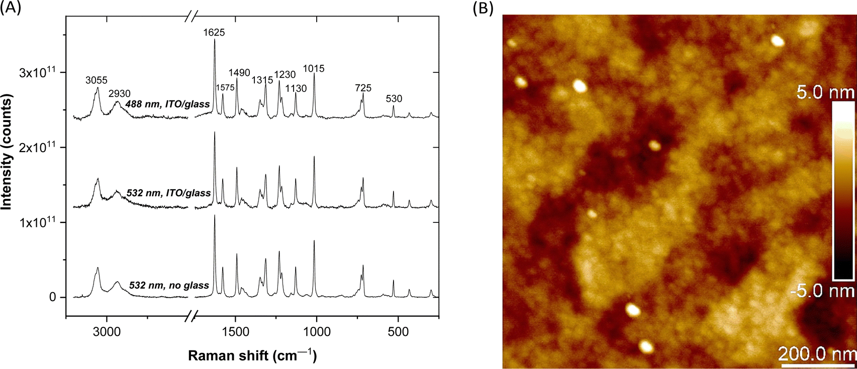 | ||
| Fig. 1 (A) Raman spectra of PCaPMA powder with and without ITO|glass cover, with 488 and 532 nm excitation laser, respectively. The spectra are scaled and shifted to enable comparison, the displayed peak maxima are rounded within 5 cm−1, (B) AFM image of a thin film cast on ITO|glass substrate (tapping mode, 2D scan with a height sensor). | ||
Comparison of powder and thin film spectra showed that all the bands present in thin film spectra also appear in powder spectra. For the thin film, one-scan spectra were acquired at five to fifteen different locations within the ITO|PCaPMA|Al device under each applied voltage. Excellent spectral reproducibility was confirmed for the band positions, relative intensities, and luminescent background, which is highly relevant for the in situ Raman spectra analysis presented below.
PCaPMA spin-cast from chlorobenzene solution forms relatively homogenous films, with surface roughness in the order of several nanometres. Even in extremely thin film (∼30 nm), the roughness was below 3 nm when scanned by AFM at 0.5 Hz over the surface of the layer cast on ITO (Fig. 1B and Fig. S2, ESI†). No pinholes were detected when measured over multiple regions; the bright spots originate from dust particles.
Electrical characterization: mimicking synaptic plasticity
Voltage-induced resistance changes were measured through current–voltage (I–V) characteristics of ITO|PCaPMA|Au or Al devices. The ability of the device to emulate the temporal effect of action potentials on the synaptic connection was tested applying a continuous train of voltage pulses with varied parameters: amplitude, pulse duration, frequency, and counts. First, trigger pulses with a pulse duration of 10 ms and amplitudes of 500 mV were employed to stimulate the conductance changes. The current level was then monitored by a 50 ms read pulse with the amplitude of −50 mV following 20 ms of each trigger pulse (Fig. 2) unless otherwise stated. Analog changes in device conductance were observed over 200 continuous measurements and no complete overlap in conductance level was observed before saturation. The increase was observed when the negative bias was applied to the top electrode, indicating the prolonged strengthening of the synapse (potentiation). The reverse pulses of the same amplitude and pulse duration caused the current decrease, indicative of depression that signifies the weakening of the synaptic connection. As the conductance increase was caused when the bias was applied through TE, analogically, this electrode is considered to be a pre-synaptic terminal, and the current flowing through the device is referred to as an excitatory-post-synaptic current (EPSC).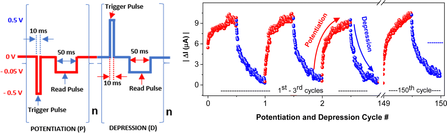 | ||
| Fig. 2 Left panel: Schematic diagram of pulses applied for synaptic weight modulation, comprising 200 consecutive potentiation pulses (amplitude: −500 mV, pulse width: 10 ms), followed by 200 successive depression pulses (+500 mV; 10 ms). Monitoring was performed using reading pulses (−50 mV, 50 ms duration, current integration time: 20 ms) applied 20 ms after each potentiation pulse (red dots) or depression pulse (blue dots). Right panel: The current response over 150 P/D successive cycles. | ||
The device exhibits high reproducibility of conductance changes over 150 measured cycles. These measurements were conducted at room temperature in an ambient environment, without any observed degradation of electrical characteristics during multiple cycles (Fig. 2) A continuous conductance increase was observed until its saturation value. Similar behaviour was observed on devices with Al TE, but the conductance changes were smaller (Fig. S4, ESI†). It is the analogy of usual properties known for long-term potentiation, indicating the saturation of learning and blocking new learning.8 Subsequently, pulses of reversed polarity cause the current to be decreased, similar to LTD in a neural synapse. These potentiation and depression sequences were repeated over 150 cycles and no marked deviation from the above-described behaviour was observed. Moreover, similar finding of analog changes in device conductance was observed during 20 repeated scans in which the voltage swept from 0 to ± 0.5 V and then reversed back to 0 V at a rate of 0.5 V s−1, as shown in Fig. S3 (ESI†). These properties underscore the potential of memristors to emulate the cognitive information processing as observed in the brain.22,42,43
In Fig. S5A (ESI†) three subsequent potentiation/depression cycles for devices of four different thicknesses of the active layers are shown. These measurements employed a standard pulse setup with 100 potentiation-only and 100 depression-only pulses in each cycle. As expected, the measured current decreased with the increasing thickness but, with the exception of the thinnest devices where the saturation was less pronounced, the trends of all P/D cycles were very similar. The statistical distributions of relative changes of conductance between two limiting saturation values of P/D cycles acquired on 70 randomly selected samples having the same four thicknesses are shown in Fig. S5B (ESI†). It can be seen that majority of the samples show the conductivity increase by potentiation between 50 to 75% of the initial value. With increasing thickness, the relative changes become less in average, being only between 25 to 50% for the devices with 142 nm thick active layer. Detailed thickness-dependent changes and their statistical distribution in reproducibility are summarized in Fig. S5 (ESI†).
Influence of frequency and amplitude of trigger pulses
Five potentiation/depression (P/D) cycles, each comprising 200 potentiation pulses, followed by equal number of depression pulses were employed in order to document the sensitivity of the conductance changes on various parameters. First, trigger pulses of five different amplitudes: ±0.1 V, ±0.2 V, ±0.3 V, ±0.4 V, and ±0.6 V were used. Notably, a trigger pulse amplitude of 100 mV produced only a 2 μA potentiation, while 600 mV produced a 12 μA change (Fig. 3A). In the second measurement, the effect of the pulse width variations was tested (Fig. 3B). Even a pulse as short as 5 ms triggered the device response. When measured with different time intervals between the trigger and read pulse (Δt), the synaptic plasticity was found to increase with shortening the interval (Fig. 3C). The temporal learning efficacy with a wider gap was lower. For instance, for Δt = 1 s, the potentiation nearly fades, and it is completely extinguished when measured 5 seconds after the trigger pulse. As in the study reported by Xi Yang, et al.,44PCaPMA demonstrated similar spike-rate dependent plasticity of conductance changes in the frequency interval 1 Hz to 40 Hz (Fig. 3C). | ||
| Fig. 3 Progression of conductance changes triggered by a sequence of trigger pulses of different amplitude (A), pulse width (B), and delay time Δt between trigger and reading pulses (C), keeping other parameters constant at standard value: trigger pulses with amplitude ± 500 mV and pulse width 10 ms, number of pulses 200, delay time between trigger and read pulse Δt 20 ms. P/D stands for Potentiation/Depression. | ||
The conductance changes under different numbers of trigger pulses are shown in Fig. S6 (ESI†). The device prominently followed the same course of evolution for each run repeated after a prolonged time-gap. The degree of alteration in conductance typically diminishes after each trigger pulse, however only a minimal change was observed after 80–100 triggers, suggesting a tendency toward synaptic saturation. For various number of trigger pulses used in a single potentiation cycle ranging between 10 and 1000, the conductance channel modulation was increased with increase in pulse numbers. After 500 consecutive potentiation trigger pulses, the device exhibited nearly negligible potentiation with an increased signal noise, indicative of synaptic saturation. However, some increase in conductance is still observable even with 1000 trigger pulses (Fig. S6, ESI†). Similarly, in Fig. S7 (ESI†), when the frequency of trigger spikes exceeds 3 Hz, long-term potentiation began to saturate. This indicates the trend of the device towards learning and saturation. All data shown in Fig. 3 and Fig. S7 (ESI†) point to a similarity with biological synapses: trigger pulses with a longer pulse width or higher amplitudes have a bigger effect, whereas increasing the delay time results in a smaller response.
Short to long-term memory transition
The following study has been made illustrating the impact of stimulating pulse frequency on the plasticity alteration and on the retention capacity (Fig. 4). Subsequent to each trigger pulse, the current was measured by ten reading pulses that monitored the immediate conductance. The red dots indicate the first conductance level taken immediately after 10 ms of trigger. Although the capacitive effect was observed in shorter time scale this first point might still include its contribution. Overall trigger pulse repetition rate below 1 Hz allowed almost full relaxation to its initial conducting state (Fig. 4, left panel) resembling the short-term potentiation (STP), i.e., the memory-fading process in the human brain after a weak stimulation. Such volatile memorization serves only for the decoding of temporal information in biological systems.45 However, as shown in Fig. 4, right panel, and Fig. S7A (ESI†), an elevated frequency of the trigger pulses above 1 Hz enhances the conductance state of the device with partial preservation of conductance from each stimulation, illustrating the emulation of long-term potentiation (LTP). The transition from STP to LTP occurred at a trigger frequency higher than 1 Hz (Fig. S7A, ESI†), while further increase in frequency facilitated a rapid LTP evolution responsible for the memory transition from short-term memory (STM) to long-term memory (LTM). This behaviour is further depicted in Fig. S7B and C (ESI†). Five consecutive potentiation cycles followed by consecutive depression cycles are shown, each cycle comprising a train of 50 consecutive pulses and separated from the next cycle by 10 s interval, with the pulse application scheme as shown in Fig. 2.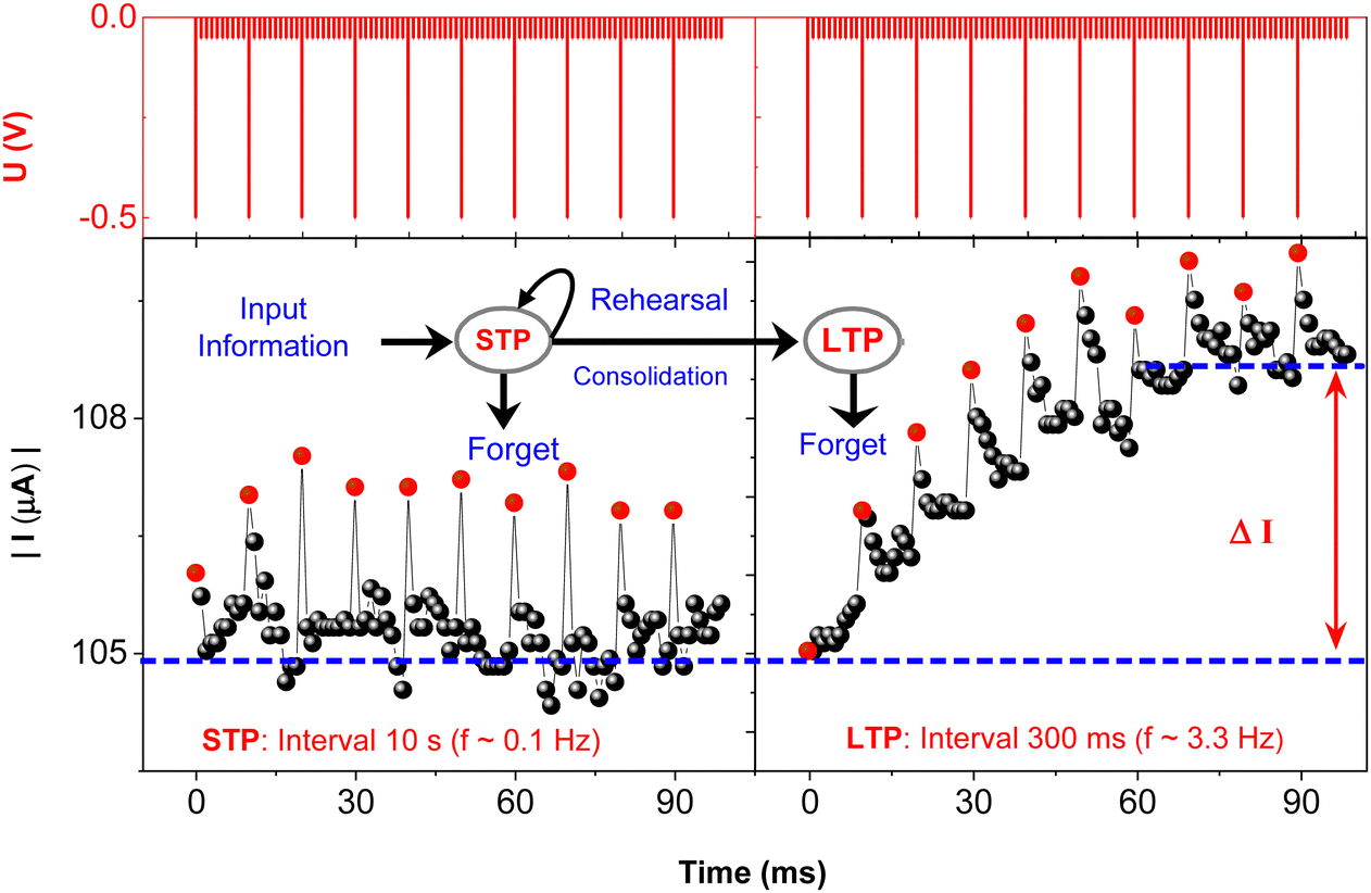 | ||
| Fig. 4 Progression of conductance changes during stimulation by trigger pulses at different frequencies: 0.1 Hz (left), implying a time interval between two subsequent triggers Δt = 10 s, and 3.3 Hz (right), i.e. Δt = 300 ms. Following each trigger pulse, the current was monitored using 10 successive reading pulses. The inset shows a diagram of learning and memory retention during the rehearsal process as adapted from ref. 5. | ||
After the relaxation interval of 10 s, during which no trigger pulse was applied, the conductance sharply dropped down, mimicking STM, yet it did not entirely revert to the original state. The excitation over four subsequent cycles caused a similar increase in conductance as in the preceding cycle but with initial current level shifting to higher values, thus illustrating the LTM. By applying trains of pulses with opposite polarity, the reversed process was observed, imitating short- term and long-term forgetting (STF/LTF). It is illustrated that the repetition of potentiation only or depression only cycles creates stronger or weaker connection, respectively, similar as observed in biological species. Utilization of this effect, SNNs can extensively contribute to the development in artificial intelligence, namely in associative learning and training. For example, the repeated triggering of these signals in a certain time frame trains the device to enable its classical conditioning by pairing the neutral stimulus to conditioned stimulus, as described by Pavlov in the experiment with his dog.46–48 In our device, such pairing with the voltage pulses was also achieved (Fig. S8, ESI†). Although the signals used in our study were mostly higher compared to biological systems, it can be seen from Fig. 3A that the effects are observable also at lower signal amplitudes but the S/N ratio is much lower.
Simulation of paired-pulse facilitation/depression and spike-timing dependent plasticity
The analysis of paired-pulse facilitation/depression (PPF/D) provides a deeper understanding of the short-term plasticity, revealing the temporal correlation between conductance changes with two concurrent stimuli.45 The PPF is a short-term, activity-driven process common to the most chemically transmitting synapses.49 It refers to an enhancement in the amplitude of the second of two rapidly evoked excitatory post-synaptic potentials (EPSPs). The second stimulus can either boost or diminish the response, resulting in PPF or PPD, respectively. This change depends on the time interval between the two excitatory pulses. As depicted in Fig. S9 (ESI†), stimulation of the conductance was performed using a pair of voltage pulses with a pulse interval (Δt) of 50 ms between them. A1 and A2 denote the current monitored by the reading pulses after 5 ms following the first and second stimulation, respectively. For PPF, the amplitude A2 was enhanced compared to A1, while for PPD, A2 was suppressed. This change defines the PPF/D index, which was calculated for 45 pulse pairs with randomly varying intervals Δt obtained by using following equation:50 | (1) |
The dependence of the PPF/D index on the time interval between trigger pulses Δt is shown in Fig. 5A. Before each PPF/D measurement, the sample was left to relax for 5 min without any excitation. Decreasing the interval between pulses enhanced the memory effect of the pre-spiking pulse on the subsequent one.
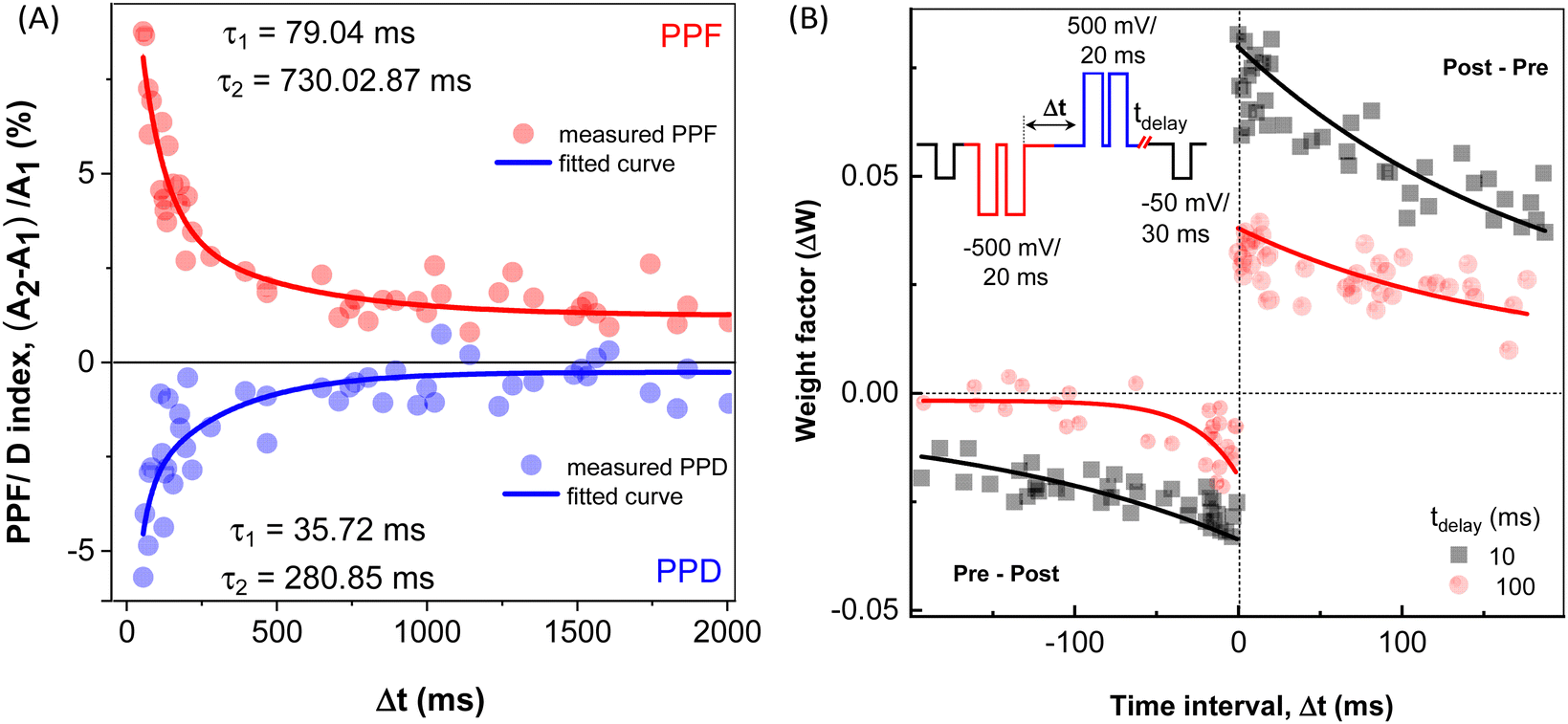 | ||
| Fig. 5 (A) The dependence of PPF (red symbols) and PPD (blue symbols) on randomly varying inter-spike time interval Δt. Red and blue lines – double exponential fits according to eqn (2). (B) Dependence of the synaptic weight ΔW calculated according to eqn (3) on the time interval Δt between the pre- and post-synaptic spikes for two different time delays: tdelay = 10 ms (black squares), and tdelay = 100 ms (red circles) and full lines – fits calculated using eqn (4). Inset: Schematic showing the sequences of pre-synaptic (red) and post-synaptic (blue) pulse pairs. | ||
The obtained values were then fitted using the double exponential function, following the equation:
| PPF/D index = C0 + C1e−Δt/τ1 + C2e−Δt/τ2 | (2) |
| Stimulation | Scaling factors (%) | Relaxation time (ms) | |||
|---|---|---|---|---|---|
| C 0 | C 1 | C 2 | τ 1 | τ 2 | |
| PPF | 1.2 | 9.0 | 2.9 | 79 | 730 |
| PPD | 0.5 | −7.0 | −3.5 | 35 | 280 |
Additionally, spike-timing dependent plasticity (STDP) shows the plasticity features of inter-neuronal connections, based on the sequence and temporal separation between pre-synaptic and post-synaptic spikes.51–54 When the pre-synaptic spike precedes the post-synaptic spike (positive time delay, Δt > 0), the synaptic weight increases, resulting in the potentiation, LTP. Conversely, when the order is reversed (Δt < 0), the synaptic weight diminishes, leading to the depression, LTD.54 STDP is also an activity-driven mechanism that constitutes an important principle of competitive Hebbian learning, serving as a basis of for cognitive learning.55 STDP of the studied structure is documented in Fig. 5B. Here, a couple of trigger pulse doublets (square waves, amplitude 500 mV, pulse duration 20 ms separated by 10 ms) were applied to Au and ITO electrodes, representing the pre-synaptic and post-synaptic neurons, respectively, (inset of Fig. 5B), similarly as reported by C–S. Yang et al.56 The conductance change was then monitored after two distinct time delays (tdelay = 10 ms and 100 ms) for both spike pair orders. As in the PPF/D, each STDP measurement was carried out with random sampling that consisted of 45 sequences with randomly selected time intervals Δt ranging from 0 to 200 ms, as illustrated by the scheme in the inset of Fig. 5B. Between each subsequent STDP assessment, the device was allowed to relax for 5 min to avoid any history-dependent current response from the preceding measurement. An increase in conductance (ΔG > 0) was observed for Δt > 0 indicating the strengthening of the synaptic connection, and a weakening of the synapse (i.e. reduction in its conductance, ΔG < 0) was achieved for Δt < 0. The relative synaptic weight change (weighting factor, ΔW) is then calculated using eqn (3):51
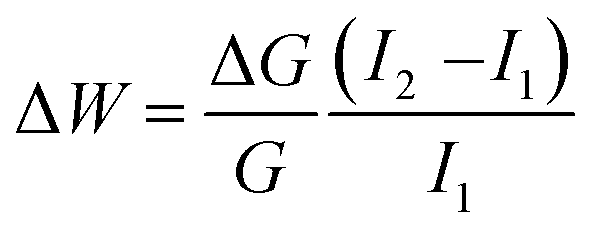 | (3) |
I 1 and I2 denote current after and before pre- and post-spikingpairs. The experimentally measured weighting factors are fitted using the equation:
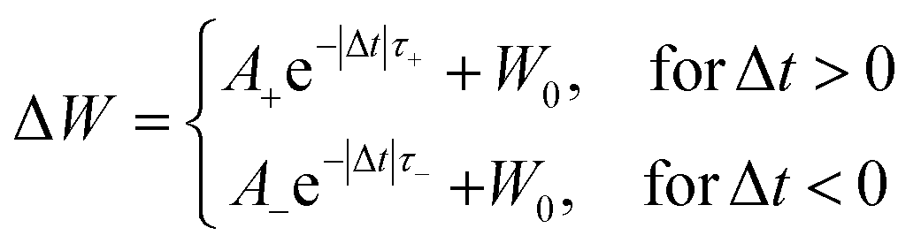 | (4) |
| Spikes order | Time delay, tdelay (ms) | Asymptotic value, W0 | Scaling factor, A+/− | Relaxation time, τ+/− (ms) |
|---|---|---|---|---|
| Pre-Post (Δt > 0) | 10 | 0.012 | 0.07 | 190 |
| 100 | 0.005 | 0.30 | 160 | |
| Post-Pre (Δt < 0) | 10 | 0.008 | 0.03 | 180 |
| 100 | −0.002 | 0.02 | 27 |
Discussion of working mechanisms
There have been several mechanisms reported in the literature for the explanation of the memristive phenomena. Among them, electrochemical metallization,20 valence change,59 and thermochemical21 mechanisms are the most frequently reported. These mechanisms are based on a reversible formation of conducting filaments, in the first case composed of reduced metal ions penetrating the layer from the metal electrode, in the latter two cases composed of oxygen vacancies in metal oxides that are part of the active layer. These mechanisms are, however, typical for inorganic memristors, whereas the mechanisms such as space charge formation combined with trapping/detrapping processes, D–A charge transfer and redox reactions, and conformation changes in the polymer backbone and side groups are typical for organic materials.23,33,42,60–62 As mentioned in the introduction, polymers like PCaPMA have the ability to undergo voltage-induced conformational changes causing reorganization of the carbazole units, and hence modifying their mutual interactions. The continuous extension in overlapping of these functional units broadens the conducting path under application of trigger voltage pulses, while the reverse polarity breaks the pre-assigned overlap of these groups, resulting in a decrease of polymer conductivity. The rotation of carbazole units and filling/detrapping rate determine switching/resetting speed.33 Although not quantified in this manuscript, the transition time scale for the carbazole rearrangement can be estimated from the gamma relaxation time around 0.1 to 1 ms obtained by impedance spectroscopy reported in our previous work.33Fig. S10 (ESI†) shows the representative band diagram of the ITO|PCaPMA|Au or Al devices indicating the adjustment of the energy barrier at the metal–organic interface. With the HOMO level of the PCaPMA, EHOMO = −5.23 eV, and the work function of gold (5.1 eV),63 smaller Schottky barrier of only 0.13 eV makes Au electrode a better injecting contact, in contrast to aluminium. PCaPMA also contains localized states in the bulk with the potential depth φt,33 which act as charge trapping centres. These trapping sites get occupied by carriers injected from the electrode, continuously capturing charges within their characteristic time scales. The current decay in the triggered device, when monitored after a prolonged time in the timescale of tens to hundreds of milliseconds range, suggests the release of previously trapped carriers from the shallow traps with depth less than 0.9 eV.64 With the increasing frequency of triggering, i.e. under faster stimulation, the charges fill the localized levels continuously, increasing the device conductance throughout a longer timescale. Reversing the polarity, these trapped carriers are released resulting in decreased conductivity. This charging/discharging is continued until the saturation is reached.
Spectro-electrochemical measurements
As an alternative mechanism, we also considered the effect of redox reaction in the polymer driven by varying applied potential. Spectro-electrochemical data shown in Fig. 6A, clearly depict the increase of optical absorption bands centred at the wavelengths 333 nm and 346 nm, correlated with the oxidation of the functional carbazole units. During oxidation, one lone pair electron from the carbazole or amide group present in the side groups is lost forming a positive polaron (depicted in Fig. 6B) and the charge is balanced by the counter ions (A−).31 This shifts the energy levels of the molecule significantly, driving the conformational reorganization of carbazole units that change their mutual interaction, resulting in the enhancement of the channel conductance. With reverse polarity, the polymer is reduced back to the neutral state, as documented by the recovery of the original optical absorption, resetting the original conformation of the side groups and, consequently, decreasing conductance of the system.65 These redox phenomena and conductance changes follow well the observed LTP and LTD of the device.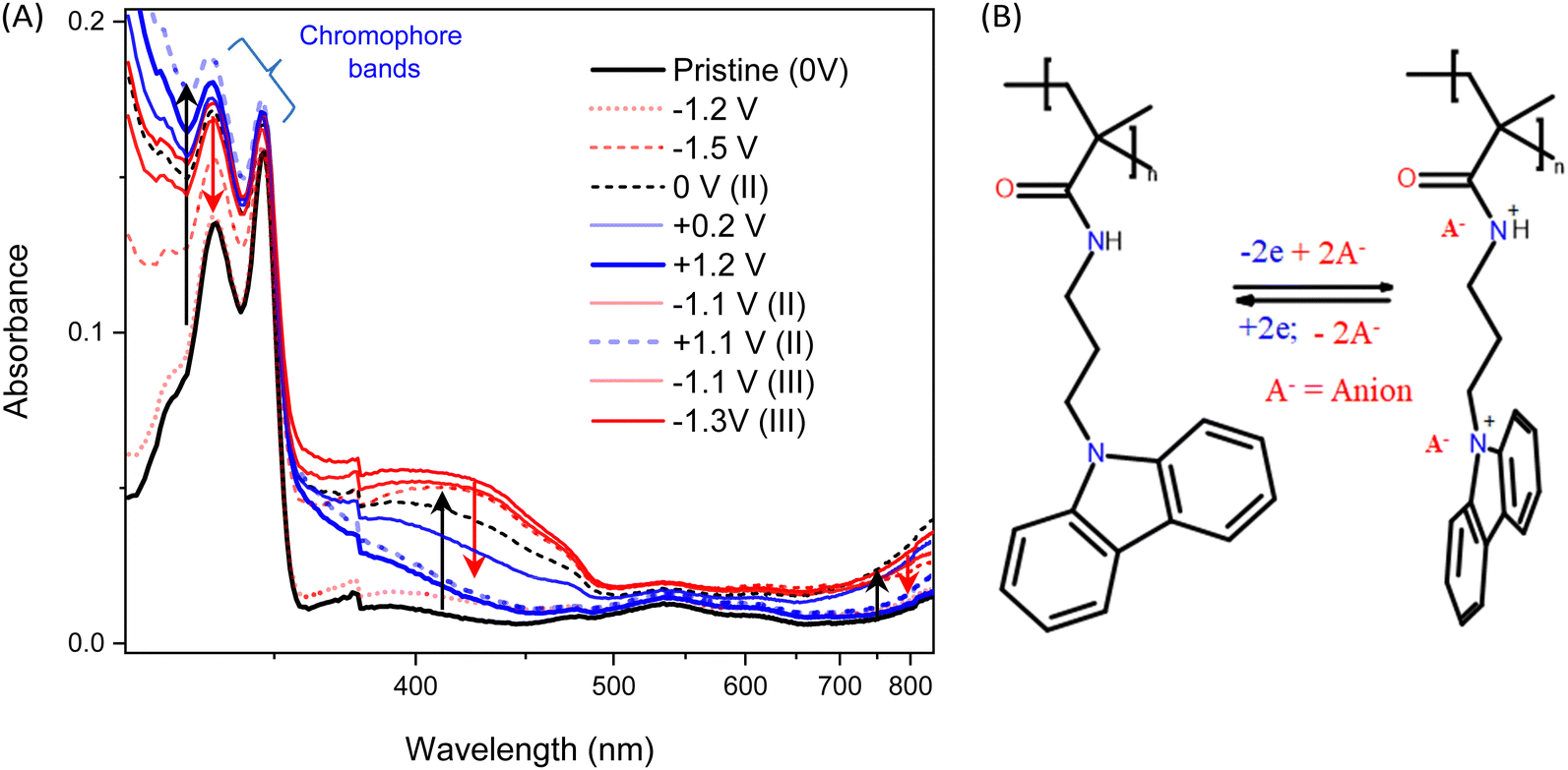 | ||
| Fig. 6 (A) UV-vis spectra of the ITO|PCaPMA|electrolyte|ITO device recorded under different applied voltage. (Red and blue curves with +V and −V, respectively, and inset as the zoomed spectra in NIR region). (B) Schematic of redox reaction and voltage-induced conformation of carbazole units similarly as in ref. 31. | ||
In situ Raman spectroscopy under applied voltage
Many of the bands present in the powder spectra (Fig. 1A) are also found in the in situ Raman spectra of ITO|PCaPMA|Al devices, as documented in Fig. S11 and S12 (ESI†) for PCaPMA layer thickness of 550 and 175 nm, respectively, measured under various applied voltages. Some bands are missing from the in situ spectra since the sampled layer was too thin to detect them – the overall intensity of PCaPMA bands was very low. Despite sampling various positions by the excitation laser under each electric field strength used and with different current compliances, reproducible spectra were obtained without any changes in positions and relative intensities of the Raman peaks. This is documented by the difference spectra presented in the lower panels of Fig. S11 and S12 (ESI†). Such lack of spectral change indicates that the material remains stable and no conductive filaments were formed between two electrodes through the active layer. This observation; however, does not exclude probable changes to the hydrogen bonding of the amide group in PCaPMA, since the corresponding Raman bands were likely obscured by bands of other groups.66When the device with the thicker PCaPMA layer (550 nm) was in the ON state and excitation laser light of 488 nm was applied (Fig. S11, ESI†), a broad luminescence band was detected with its maximum shifting between 700–800 cm−1 (equivalent to 510 nm in fluorescence spectra shown in Fig. S13, ESI†). The intensity of the newly present luminescence was dependent on several parameters – including the applied electric field and its duration, as well as the intensity and duration of the Raman excitation, and significantly decreased when the device was returned to the OFF state. Similarly, the application of an electric field caused reversible changes in in situ voltage-dependent fluorescence emission spectra measured under excitation at 333 nm (Fig. S13, ESI†), confirming the impact of the applied field observed by Raman spectroscopy. This band peaking at 510 nm, albeit weak, was also observable and persisted in the fluorescence spectra of the layer under excitation with 488 nm light. However, no emission was observed under a similar applied electric field but without light excitation, suggesting that electroluminescence as an origin of this emission can be excluded.
Under Raman excitation of the device with the thinner (175 nm) PCaPMA layer by laser light 532 nm, another new broad structureless emission band centred around 2500 cm−1 appeared, exhibiting increased intensity under positive bias and diminishing reversibly and completely when the device was returned to the OFF state. Although the origin of this band remains unclear and was not observed by fluorimetry, it is likely attributed to phosphorescence or to the emission from impurity sites.67
The two luminescence phenomena associated with the fluorescence band in the device with a thicker layer, and the probable phosphorescence phenomenon observed in the device with the thinner layer might arise from dynamic changes in trapping site occupation, which provides further support for our previous conclusion that the trapping/detrapping process underlies the resistive switching mechanism of the memory device.33
Conclusions
We demonstrate that the memristor formed of a sandwich structure with PCaPMA as an active layer can emulate the functionality of biological synapses. Its resistance can be continuously varied upon the excitation by voltage pulses, depending on their polarity, amplitude, and frequency. The observed properties closely resemble neurosynaptic features, related to both short- and long-term plasticity, responding well to moderate ±500 mV stimulating voltage pulses. Persistent stimulation induces prolonged changes in the layer conductance, whereas weaker inputs lead to a volatile memorization. The memory transition was observed already above 1 Hz repetition rate of stimulating pulses. The device is capable of associative learning via pairing of neutral stimuli with conditioned stimuli, similar to the experiment carried out by Pavlov stimulating the dog's salivation.The tendency of carbazole functional units to undergo conformational changes and redox reactions governs the resistance changes in the system. The manipulation of trapping sites occupation, along with the improved injection from the contact that enhances charge carrier injection also supports the suggested underlying mechanism. The device meets the fundamental requirements of the synapse, addressing both short-term and long-term plasticity, as demonstrated by PPF/D and STDP characteristics. It shows the potential of memristors with PCaPMA active layer for application in neuromorphic computing and eventually for use in AI systems.
Author contributions
YRP: investigation – device design and preparation, electrical and optical study, writing original draft, AP: investigation – electrochemical measurements, AŠ: investigation – Raman spectroscopy, DV: investigation – polymer design and synthesis, SHF: validation, JP: conceptualization, funding acquisition, supervision and writing – review & editing.Data availability
The source data of PPF/PPD and STDP can be accessed from Zenodo at https://zenodo.org/records/12685756.Conflicts of interest
There are no conflicts to declare.Acknowledgements
The authors thank the Czech Science Foundation, project No. 24-10384S, for funding. Additionally, the authors would like to acknowledge Oleksii Kotko for the help with the AFM measurement.Notes and references
- C. Prakash, L. R. Gupta, A. Mehta, H. Vasudev, R. Tominov, E. Korman, A. Fedotov, V. Smirnov and K. K. Kesari, Mater. Adv., 2023, 4, 5882–5919 RSC.
- A. Citri and R. C. Malenka, Neuropsychopharmacology, 2008, 33, 18–41 CrossRef PubMed.
- A. E. Pereda, Nat. Rev. Neurosci., 2014, 15, 250–263 CrossRef CAS.
- B. Hille, Ion channels of excitable membranes, Sinauer associates, Inc., Sunderland, USA, 1985 Search PubMed.
- T. Chang, S.-H. Jo and W. Lu, ACS Nano, 2011, 5, 7669–7676 CrossRef CAS.
- T. Ohno, T. Hasegawa, T. Tsuruoka, K. Terabe, J. K. Gimzewski and M. Aono, Nat. Mater., 2011, 10, 591–595 CrossRef CAS PubMed.
- R. M. Mulkey and R. C. Malenka, Neuron, 1992, 9, 967–975 CrossRef CAS.
- S. J. Martin, P. D. Grimwood and R. G. M. Morris, Neuroscience, 2000, 23, 60456 Search PubMed.
- C. Mead and M. Ismail, Analog VLSI implementation of neural systems, Kluwer Academic Publishers, Massachusetts, 1989 Search PubMed.
- H. Bian, Y. Y. Goh, Y. Liu, H. Ling, L. Xie and X. Liu, Adv. Mater., 2021, 33, 2006469 CrossRef CAS.
- S. Choi, J. Yang and G. Wang, Adv. Mater., 2020, 32, 2004649 Search PubMed.
- S. Liu, X. Chen and G. Liu, Polym. Int., 2021, 70, 374–403 CrossRef CAS.
- Z. Cao, B. Sun, G. Zhou, S. Mao, S. Zhu, J. Zhang, C. Ke, Y. Zhao and J. Shao, Nanoscale Horiz., 2023, 8, 716–745 RSC.
- L. Chua, Semicond. Sci. Technol., 2014, 29, 104001 CrossRef.
- S. P. Adhikari, M. P. Sah, H. Kim and L. O. Chua, IEEE Trans. Circuits Syst. I Regul. Pap., 2013, 60, 3008–3021 Search PubMed.
- S. G. Kim, J. S. Han, H. Kim, S. Y. Kim and H. W. Jang, Adv. Mater. Technol., 2018, 3, 1800457 CrossRef.
- Y. Yu, M. Xiao, D. Fieser, W. Zhou and A. Hu, J. Mater. Chem. C, 2024, 12, 3770–3810 RSC.
- P. Hu, S. Wu and S. Li, Advances in Memristor Neural Networks - Modeling and Applications, IntecOpen, London, 2018 Search PubMed.
- W. Sun, B. Gao, M. Chi, Q. Xia, J. J. Yang, H. Qian and H. Wu, Nat. Commun., 2019, 10, 3453 CrossRef.
- I. Valov, R. Waser, J. R. Jameson and M. N. Kozicki, Nanotechnology, 2011, 22, 254003 CrossRef PubMed.
- J. J. Yang, I. H. Inoue, T. Mikolajick and C. S. Hwang, MRS Bull., 2012, 37, 131–137 CrossRef CAS.
- Y. Chen, G. Liu, C. Wang, W. Zhang, R.-W. Li and L. Wang, Mater. Horiz., 2014, 1, 489–506 RSC.
- A. Pandey, A. Chernyshev, Y. R. Panthi, A. Sturcov, O. Kocková, S. H. Foulger, J. Vohlidal and J. Pfleger, Polymers, 2024, 16, 542 CrossRef CAS PubMed.
- S. Shin, D. C. Kang, K. Kim, Y. Jeong, J. Kim, S. Lee, J. Y. Kwak, J. Park, G. W. Hwang, K.-S. Lee, J. K. Park, J. Li and I. Kim, Mater. Adv., 2022, 3, 2827–2837 RSC.
- Z. Shen, C. Zhao, Y. Qi, W. Xu, Y. Liu, I. Z. Mitrovic, L. Yang and C. Zhao, Nanomaterials, 2020, 10, 1437 CrossRef CAS.
- W. Wang, W. Song, P. Yao, Y. Li, J. Van Nostrand, Q. Qiu, D. Ielmini and J. J. Yang, iScience, 2020, 23, 101809 CrossRef.
- Y. Li, Q. Qian, X. Zhu, Y. Li, M. Zhang, J. Li, C. Ma, H. Li, J. Lu and Q. Zhang, InfoMat, 2020, 2, 995–1033 CrossRef CAS.
- S. H. Foulger, Y. Bandera, B. Grant, J. Vilčáková and P. Sáha, J. Mater. Chem. C, 2021, 9, 8975–8986 RSC.
- T. McFarlane, Y. Bandera, B. Grant, B. Zdyrko, S. H. Foulger, J. Vilčáková, P. Sáha and J. Pfleger, Adv. Electron. Mater., 2020, 6, 2533 RSC.
- Q. Ling, Y. Song, S. J. Ding, C. Zhu, D. S. H. Chan, D.-L. Kwong, E.-T. Kang and K.-G. Neoh, Adv. Mater., 2005, 17, 455–459 CrossRef CAS.
- W. Tang, H. He, J. Shi, B. Cao, C. Yang and C. Fan, Org. Electron., 2019, 75, 105386 CrossRef CAS.
- Q.-D. Ling, D.-J. Liaw, C. Zhu, D. S.-H. Chan, E.-T. Kang and K.-G. Neoh, Prog. Polym. Sci., 2008, 33, 917–978 CrossRef CAS.
- Y. R. Panthi, J. Pfleger, D. Výprachtický, A. Pandey, M. A. Thottappali, I. Šeděnková, M. Konefał and S. H. Foulger, J. Mater. Chem. C, 2023, 11, 17093–17105 RSC.
- W.-P. Lin, S.-J. Liu, T. Gong, Q. Zhao and W. Huang, Adv. Mater., 2014, 26, 570–606 CrossRef CAS.
- H.-J. Yen and G.-S. Liou, Polym. J., 2016, 48, 117–138 CrossRef CAS.
- T. M. McFarlane, B. Zdyrko, Y. Bandera, D. Worley, O. Klep, M. Jurča, C. Tonkin, S. H. Foulger, J. Vilčáková, P. Sáha and J. Pfleger, J. Mater. Chem. C, 2018, 6, 2533–2545 RSC.
- S.-L. Lim, Q. Ling, E.-Y. H. Teo, C.-X. Zhu, D. S.-H. Chan, E.-T. Kang and K.-G. Neoh, Chem. Mater., 2007, 19, 5148–5157 CrossRef CAS.
- F. C. Whitmore, H. S. Mosher, R. R. Adams, R. B. Taylor, E. C. Chapin, C. Weisel and W. Yanko, J. Am. Chem. Soc., 1944, 66, 725–731 CrossRef CAS.
- G. Socrates, Infrared and Raman characteristic group frequencies, John Wiley & Sons, New York, 2001 Search PubMed.
- A. Bree and C. Taliani, Chem. Phys. Lett., 1983, 98, 62–65 CrossRef CAS.
- W. Lao, C. Xu, S. Ji, J. You and Q. Ou, Spectrochim. Acta, Part A, 2000, 56, 2049–2060 CrossRef PubMed.
- A. S. Sokolov, H. Abbas, Y. Abbas and C. Choi, J. Semicond., 2021, 42, 013101 CrossRef.
- L. F. Abbott and S. B. Nelson, Nat. Neurosci., 2000, 3, 1178–1183 CrossRef CAS PubMed.
- X. Yang, C. Wang, J. Shang, C. Zhang, H. Tan, X. Yi, L. Pan, W. Zhang, F. Fan, Y. Liu, Y. Chen, G. Liu and R.-W. Li, RSC Adv., 2016, 6, 25179–25184 RSC.
- D. V. Buonomano, J. Neurosci., 2000, 20, 1129–1141 CrossRef CAS PubMed.
- M. Adams, Theory Psychol., 2014, 30, 121–141 CrossRef.
- M. Kumar, S. Abbas, J. H. Lee and J. Kim, Nanoscale, 2019, 11, 15596–15604 RSC.
- I. P. Pavlov, Ann. Neurosci., 2010, 17, 153 Search PubMed.
- R. S. Zucker and W. G. Regehr, Annu. Rev. Physiol., 2002, 64, 355–405 CrossRef CAS PubMed.
- P.-P. Lu, D.-S. Shang, C.-S. Yang and Y. Sun, J. Phys. D: Appl. Phys., 2020, 53, 485102 CrossRef CAS.
- Y. Li, Y. Zhong, J. Zhang, L. Xu, Q. Wang, H. Sun, H. Tong, X. Cheng and X. Miao, Sci. Rep., 2014, 4, 4906 CrossRef CAS PubMed.
- M. C. W. van Rossum, G. Q. Bi and G. G. Turrigiano, J. Neurosci., 2000, 20, 8812–8821 CrossRef CAS.
- L. Wang and C. A. Alexander, J. Comput. Sci. Appl., 2020, 7, 56–61 Search PubMed.
- B. Linares-Barranco and T. Serrano-Gotarredona, Nat. Preced., 2009, 2–5 Search PubMed.
- R. C. Froemke and Y. Dan, Nature, 2002, 416, 433–438 CrossRef PubMed.
- C.-S. Yang, D.-S. Shang, N. Liu, E. J. Fuller, S. Agrawal, A. A. Talin, Y.-Q. Li, B.-G. Shen and Y. Sun, Adv. Funct. Mater., 2018, 28, 1804170 CrossRef.
- A. Thomas, A. N. Resmi, A. Ganguly and K. B. Jinesh, Sci. Rep., 2020, 10, 12450 CrossRef CAS.
- Y. Ren, C.-L. Chang, L.-Y. Ting, L. Zhou, J.-Y. Mao, S.-R. Zhang, H.-H. Chou, J.-Q. Yang, Y. Zhou and S.-T. Han, Adv. Intell. Syst., 2019, 1, 1900008 CrossRef.
- R. Waser, R. Dittmann, C. Staikov and K. Szot, Adv. Mater., 2009, 21, 2632–2663 CrossRef CAS.
- E. Omar, H. Aly and M. Fedawy, Int. J. Adv. Eng. Bus. Sci., 2023, 4, 171–198 Search PubMed.
- S. Erokhina and L. Pastorino, Phys. Status Solidi C, 2015, 12, 175–180 CrossRef CAS.
- Z. Zhao, M. E. El-Khouly, Q. Che, F. Sun, B. Zhang, H. He and Y. Chen, Angew. Chem., Int. Ed., 2023, 62, e202217249 CrossRef CAS PubMed.
- W. M. H. Sachtler, G. J. H. Dorgelo and A. A. Holscher, Surf. Sci., 1966, 5, 221–229 CrossRef CAS.
- J. Hao, R. Zou, R. Liao, L. Yang and Q. Liao, Energies, 2018, 11, 271–276 CrossRef.
- A. Betal, J. Bera and S. Sahu, J. Mater. Chem. C, 2023, 11, 4674–4682 RSC.
- D. Kurouski, T. Postiglione, T. Deckert-Gaudig, V. Deckert and I. K. Lednev, Analyst, 2013, 138, 1665–1673 RSC.
- R. Barrie and I. W. Sharpe, Can. J. Phys., 1978, 56, 550–559 CrossRef.
Footnote |
| † Electronic supplementary information (ESI) available. See DOI: https://doi.org/10.1039/d4ma00399c |
| This journal is © The Royal Society of Chemistry 2024 |