
 Open Access Article
 This Open Access Article is licensed under a Creative Commons Attribution-Non Commercial 3.0 Unported Licence
Effects of alumina priming on the electrical properties of ZnO nanostructures derived from vapor-phase infiltration into self-assembled block copolymer thin films†
Won-Il
Lee
a,
Ashwanth
Subramanian
a,
Kim
Kisslinger
b,
Nikhil
Tiwale
 *b and
Chang-Yong
Nam
*ab
*b and
Chang-Yong
Nam
*ab
aDepartment of Materials Science and Chemical Engineering, Stony Brook University, Stony Brook, New York 11794, USA. E-mail: cynam@bnl.gov
bCenter for Functional Nanomaterials, Brookhaven National Laboratory, Upton, New York 11973, USA. E-mail: ntiwale@bnl.gov
First published on 21st May 2024
Abstract
Alumina priming is frequently employed to facilitate the vapor-phase infiltration (VPI) of weakly reactive organometallic precursors into polymer templates such as self-assembled block copolymer (BCP) thin films. By first infiltrating trimethylaluminum (TMA)—a strong Lewis acid that can readily infiltrate and bind to Lewis-basic groups inside polymers—when exposed to water vapor, it produces molecular alumina terminated with a hydroxyl group. This priming step activates the polymer matrix for the following infiltration of weakly reactive organometallic precursors of a target inorganic material. Nevertheless, given the insulating nature of bulk alumina, alumina priming may negatively impact the electrical properties of the final inorganic nanostructures derived from VPI. In this study, we investigate the effects of alumina-priming on the electrical and structural properties of zinc oxide nanowires derived from VPI of diethylzinc and water into self-assembled lamellar poly(styrene-block-methyl methacrylate) (PS-b-PMMA) BCP thin films. We demonstrate facile tuning of characteristic dimension, chemical composition, and electrical conductivity of the synthesized aluminum-doped ZnO (AZO) nanowires by adjusting the TMA exposure time during a single-cycle alumina priming. Increasing the TMA exposure duration not only promotes the ZnO infiltration fidelity but also minimizes ZnO electrical resistivity at 14.3 kΩ cm at a TMA exposure duration of 100 s with a corresponding Al concentration of 6.02%. The results provide a guideline for controlling the composition, dimensions, and electrical properties of alumina-primed metal oxide nanostructures based on VPI in polymer templates.
Introduction
With the increasing demand for miniaturized electronics with improved energy efficiency and multifunctionalities, there has been a necessary decrease in the feature size of device components. State-of-the-art top-down technologies have been developed to address these needs. However, top-down lithography requires specialized equipment and sophisticated manufacturing processes, prompting the exploration of alternative methods like bottom-up lithography.1 Among these alternatives, block copolymer (BCP) lithography has emerged as a promising option. BCP lithography offers several advantages, including its cost-effectiveness, scalability, and capability to achieve highly precise nanofabrication of well-organized periodic patterns.2,3BCP self-assembly can lead to the formation of a wide variety of ordered nanostructures such as spheres, cylinders, gyroids, and lamellae dependent on the volume fractions of constituent blocks, the polymerization degree, and the degree of incompatibility between blocks (Flory–Huggins parameter, χ).4–6 These polymer nanostructures can be functionalized by a variety of hybridizing methods to exploit favorable properties of both the organic and inorganic constituents for developing high-performance materials.7,8 Poly(styrene-block-methyl methacrylate) (PS-b-PMMA), poly(styrene-block-ethylene oxide) (PS-b-PEO), poly(styrene-block-epoxyisoprene) (PS-b-PIO), poly(styrene-block-dimethylsiloxane) (PS-b-PDMS), and poly(styrene-block-2-vinyl pyridine) (PS-b-P2VP) are typical BCPs that have been used as host materials.9–13 Functional nanostructures have been achieved by using these through a range of techniques, including metal sputtering,14,15 liquid-phase infiltration (LPI),16–18 and vapor-phase infiltration (VPI).19–22
Especially, VPI, also known as sequential infiltration synthesis (SIS), is a facile method derived from ALD, in which material hybridization is attained through the infiltration of vapor-phase organometallic precursors into polymeric templates via the interaction of the Lewis-acidic organometallic precursors with the Lewis-basic functional groups in the polymer matrix.23–29 This technique can not only generate organic–inorganic hybrids but also fabricate inorganic nanostructures, replicating the initial polymer templates, such as self-assembled BCP patterns wherein block-selective infiltration of inorganic materials and following removal of the organic matrix lead to the generation of inorganic nanostructures that can have applications for membranes,30 sensors,31 energy conversion,32 and optics.33 However, since infiltration fidelity depends on the Lewis acid–base interaction between organometallic precursors (Lewis acid) and functional groups of the polar blocks in BCPs (Lewis base), it is challenging to generate nanostructures of certain target materials if required precursors have low reactivity. In principle, VPI can be applied to grow a variety of materials by adopting a suitable precursor–polymer matrix pair, as well as by tailoring the chemistry of the precursor or the functional group of the BCP template to enhance reactivity.34,35 Nonetheless, the design and modification of a novel organometallic precursor or BCP functional groups are in general non-trivial due to the complexity of chemical synthesis, while the alteration of BCP chemistry may interfere with BCP self-assembly. An alternative approach is modifying the infiltration protocols by adjusting the synthesis parameters such as temperature, pressure, exposure time, and purging time.36–38 For example, the micro-dose infiltration synthesis, which involves repeating the precursor dosing multiple times under static pressure, has been used to form ZnO nanomesh through direct infiltration of diethylzinc (DEZ) into PS-b-P2VP without pre-treatment.12 However, the highly crystalline nature of ZnO can compromise the structural integrity of the final nanostructures. Alumina priming39–41 is a widely applied technique that facilitates the formation of a variety of inorganic nanomaterials from self-assembled BCP by VPI utilizing the high reactivity of the trimethylaluminum (TMA) precursor with most of the active BCP blocks. During priming, the polymer matrix is pre-infiltrated with TMA and water to form AlOx terminated with highly reactive hydroxyl groups (strong Lewis base) within the polymer domain, enabling subsequent infiltration synthesis of other metal oxide materials using weakly reactive organometallic precursors that otherwise have insufficient block-selective reaction required for VPI. However, the alumina incorporated in the final, target inorganic material can not only alter the material structure but also its physical and chemical properties. Particularly when growing electroactive materials, the amount of pre-infiltrated alumina could potentially have a significant effect on the electrical properties of the finally synthesized structure, thus affecting the functional performances of associated electronic devices. Despite the common use of alumina priming in VPI and SIS, in-depth analysis of the effects of alumina priming on the chemical and electrical properties of synthesized materials according to priming conditions has rarely been studied.
Here, we have investigated the alumina priming effect on aluminum-doped zinc oxide (AZO) nanostructures fabricated by VPI using lamellar-patterned self-assembled PS-b-PMMA thin films. AZO is a frequently used material in the semiconductor field which has well-known properties,41,42 making it a suitable model material for examining the effect of alumina priming. Our investigation included the observation of the infiltration/structural fidelity, elemental composition, chemical (e.g., elemental distribution, crystal structure, and binding), and electronic properties of the infiltration-synthesized AZO nanostructure as a function of incorporated AlOx contents by controlling TMA exposure duration during the alumina priming cycle. This is the first report investigating the alumina priming effect on the electrical properties of the AZO nanostructure fabricated by VPI into self-assembled BCP templates. Through this paper, we elucidate how alumina priming conducted in the initial infiltration process impacted the devices and materials produced, and help establish priming conditions for synthesizing VPI-derived multifunctional materials based on these results.
Experimental
Materials
PS-b-PMMA (molecular weight (Mn) = 105 kg mol−1; 47![[thin space (1/6-em)]](https://www.rsc.org/images/entities/char_2009.gif) :58 block ratio) was purchased from Polymer Source, and PS-r-PMMA (Mn = 9.2 kg mol−1; 61:39 block ratio) was provided by The Dow Chemical Company. Propylene glycol methyl ether acetate (PGMEA), acetone, toluene, TMA, and DEZ were purchased from Sigma-Aldrich and used as received. Photoresist S1811 and MF24A developer were procured from MicroChem and used as received.
:58 block ratio) was purchased from Polymer Source, and PS-r-PMMA (Mn = 9.2 kg mol−1; 61:39 block ratio) was provided by The Dow Chemical Company. Propylene glycol methyl ether acetate (PGMEA), acetone, toluene, TMA, and DEZ were purchased from Sigma-Aldrich and used as received. Photoresist S1811 and MF24A developer were procured from MicroChem and used as received.
Preparation of self-assembled PS-b-PMMA vertical lamellar thin films
Si substrates were cleaned by oxygen plasma (20 W; 100 mTorr; 1 min) using a March CS-1701 reactive ion etcher. The brush solution (PS-r-PMMA; 1 wt% in PGMEA) was spin-cast on the cleaned Si substrate at 1500 rpm for 30 s and then at 3000 rpm for 5 s. The brush film was annealed on a N2-blanketed hot plate (Wenesco Inc., H0909AA) at 250 °C for 5 min. Excess brush polymers not grafted to the substrate were removed by rinsing with toluene, while spinning the sample at 1500 rpm for 30 s and 3000 rpm for 5 s. The lamellar-phase BCP solution (PS-b-PMMA; 1 wt% in toluene) was then spin-cast on the brush-treated Si substrate (1500 rpm; 30 s and 3000 rpm; 5 s). The resulting PS-b-PMMA BCP film was annealed on a N2-blanketed hot plate at 250 °C for 5 min to induce the self-assembled lamellar structure.Micro-dose infiltration synthesis of AZO
The infiltration synthesis of AZO into self-assembled BCP thin film templates was carried out in a commercial ALD system (Cambridge Nanotech, Savannah S200) at 85 °C using DEZ and TMA as respective metal–organic precursors along with water as an oxidant. During each precursor exposure, the chamber was under static vacuum, i.e. the chamber was isolated from the pump before pulsing the precursor and held under “static” conditions for the given exposure time. A single AlOx priming cycle was executed by pulsing the TMA valve only once for 50 ms and holding the chamber isolated from the pump for varying exposure time durations (0 to 800 s), followed by opening the chamber pumping valve and purging the chamber for 100 s using 100 sccm N2. Subsequently, a half-cycle of water exposure was implemented by pulsing the water vapor for 50 ms, holding the chamber isolated from the pump for 100 s and then purging by 100 sccm N2 for 100 s with the pump valve reopened. 6 cycles of ZnO infiltration were performed in all experiments with a microdose protocol—the DEZ valve was pulsed for 500 ms, 12 times every 30 s during the exposure period (total exposure time 12 × 30 s = 360 s) while the chamber was isolated from the pump, followed by reopening the chamber pumping valve and purging of the ALD chamber with 100 sccm N2 for 100 s. Consequently, water vapor was pulsed for 50 ms 12 times every 30 s (total exposure duration of 360 s) while the chamber was isolated from the pump, followed by 100 s purge by 100 sccm N2 with an open pump valve, completing the infiltration cycle. The infiltration synthesis was followed by the initial removal of the organic polymer matrix by oxygen plasma etching (20 W; 100 mTorr; 5 min; room temperature) and the further consolidation of the inorganic matrix and the removal of carbon impurities by O2 rapid thermal processing (RTP) treatment at 600 °C for 5 min (Modular Process Technology, RTP-600S).Fabrication of the transfer length method (TLM) device on the AZO nanostructure
A photoresist layer (S1811) was spin-cast on the AZO nanostructure generated on a SiO2 (300 nm)/Si substrate (500 rpm; 5 s and 5000 rpm; 60 s) and pre-baked on a hot plate (110 °C; 120 s). An interdigitated electrode pattern (channel length and width of ∼5 to 25 μm and 550 μm, respectively) was exposed using an MA-6 photolithography mask aligner, soaked in toluene for 1 min and blow-dried with N2 gas, post-baked on a hot plate (110 °C; 120 s) and developed in MF24A for 45 s and rinsed with deionized water for 45 s. Al/Ti/Au (120 nm/10 nm/20 nm) electrodes were thermally deposited (Lesker PVD 75), and finally, the photoresist film was lifted off in warm acetone (∼70 °C).Materials characterization
Quartz crystal microbalance (QCM) measurement was performed for in situ monitoring of mass gain of the AZO infiltration into the PS-b-PMMA matrix. The infiltration synthesized inorganic nanostructures were characterized using scanning electron microscopy (SEM, Hitachi S-4800), transmission electron microscopy (TEM, JEOL 2100, 200 kV), and scanning TEM (FEI Talos F200X, 200 kV), equipped with the energy dispersive spectroscopy (EDS) elemental mapping capability. Cross-sectional TEM samples were prepared by using a standard in situ lift-out procedure using Ga ion milling in a focused ion beam system (FEI Helios G5 UX). The elemental compositions of the prepared samples were characterized by EDS spectra using SEM (JEOL 7600F). In particular, the Al atomic composition within AZO is calculated based on the following formula: Al at%/(Al at% + Zn at%) × 100, where respective atomic concentrations of Al and Zn were obtained from EDS analysis that included Al, Zn, O, and Si (i.e., from the substrate) as the elements of interest (Table S1, ESI†). The chemical composition and defects were analyzed using X-ray photoelectron spectroscopy (XPS) on a custom-built XPS system equipped with a hemispherical electron energy analyzer (SPECS) and an Al Kα X-ray source (1486.6 eV, SPECS). The two-probe current–voltage (I–V) characteristics of AZO nanostructure devices were measured using an electrical probe station (Signatone) equipped with a dark box and a high-precision semiconductor parameter analyzer (Keithley), and channel resistivity and contact resistance of AZO nanostructures were analyzed by TLM.Results and discussion
The mechanism of block-selective VPI into BCP thin films for fabricating AZO nanostructures is depicted in Fig. 1(a). We first pretreated a SiO2/Si substrate by spin-casting a random copolymer (PS-r-PMMA) to neutralize the surface and anneal the brush layer in order to achieve surface grafting. The excessive brush layer was then rinsed with toluene while preserving the surface graft to promote a perpendicular orientation of the lamellae morphology in the subsequent PS-b-PMMA thin film. On top of the grafted substrate, an ∼35 nm PS-b-PMMA thin film was then spin-cast and annealed to form self-assembled fingerprint (lamellar) structures in response to the underlying neutral surface. Then TMA was first infiltrated into a self-assembled PS-b-PMMA film with varying exposure durations ranging from 0 to 800 s, followed by water vapor exposure for 100 s, in a single alumina priming cycle. As a strong Lewis acid, TMA reacts with Lewis basic moieties of PMMA in the initial half-cycle, and in the following half-cycle the water vapor interacts with the methyl groups of the TMA-adduct to form Al–OH species, activating the matrix for subsequent ZnO infiltration and nucleation.43 Subsequently micro-dose infiltration synthesis was carried out using DEZ and water in a cyclic manner to grow ZnO, forming infiltrated AZO molecular networks within the PMMA block. The resulting hybrid structure in the PMMA domain was converted into nanopatterned AZO by oxygen plasma etching combined with thermal annealing. Ultimately, the parallel electrodes with varying channel lengths were fabricated onto the synthesized AZO nanowires via photolithography and thermal evaporation/metal-liftoff processes.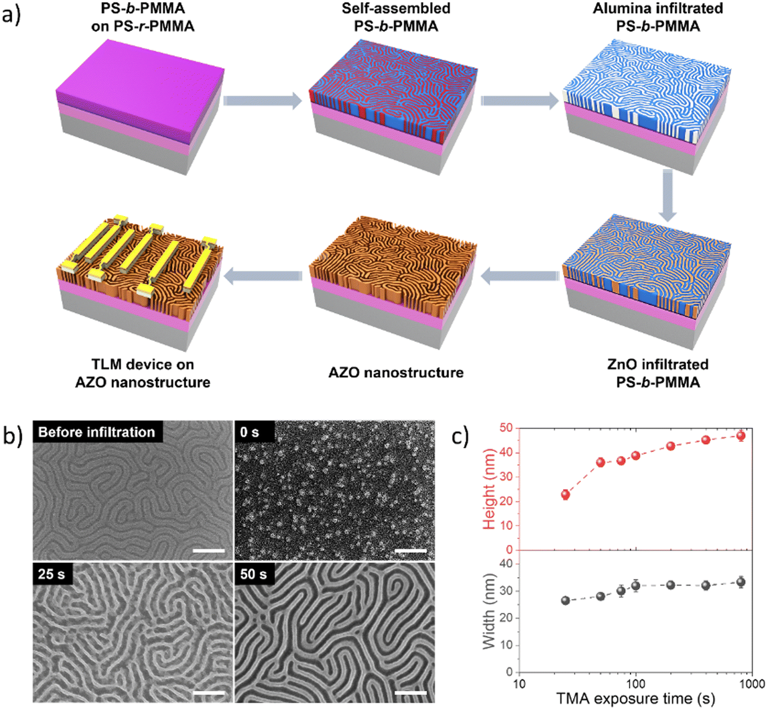 | ||
| Fig. 1 (a) Illustration of the fabrication procedure for the AZO nanostructure with alumina priming using PS-b-PMMA and TLM device electrodes. (b) Top-view of SEM micrographs of the self-assembled PS-b-PMMA BCP thin film template exhibiting a vertical lamellar morphology, and AZO nanowires synthesized by VPI with different TMA exposure times: 0 s, 25 s, and 50 s, followed by oxygen plasma/RTP treatment to remove the template (all scale bars denote 200 nm). (c) Characteristic dimension variation of AZO structures with the TMA exposure time. | ||
By controlling the TMA exposure times during infiltration, we demonstrate the tunability of AZO nanowire dimensions. SEM micrographs of self-assembled PS-b-PMMA templates generate a vertical lamellar structure with a periodic arrangement (Fig. 1(b)-top left). When the ZnO VPI was carried out without alumina priming in the starting BCP template, the BCP patterns converted to random ZnO nanoparticles as a result of the insufficient quantity of ZnO formed during the infiltration process.43 The relatively low Lewis-acidity of DEZ exhibits a lower binding tendency towards Lewis-basic moieties of PMMA, resulting in low infiltration fidelity and lack of formation of any discernable nanoarchitecture. The SEM micrograph results (Fig. 1(b)-top right and Fig. S1, ESI†) revealed that when TMA exposure during alumina priming was less than 25 s, the TMA infiltration time was too short to generate a sufficient number of the reactive sites inside PMMA, which in turn led to insufficient ZnO infiltration, therefore a continuous inorganic structure could not be formed (Fig. S1, ESI†). The VPI-synthesized ZnO with a TMA exposure time of 25 s featured nanowire fingerprint patterns with structural defects (Fig. 1(b)-bottom left). Here, although a sufficient amount of alumina priming occurred to allow the formation of continuous structures, it was insufficient to overcome the coalescing tendency of ZnO, resulting in structural defects within nanowires due to the high crystallinity of ZnO. In contrast, the ZnO nanostructures generated with TMA exposure times more than 50 s yielded a high-fidelity conversion to a distinct uniform AZO nanowire fingerprint pattern (Fig. 1(b)-bottom right). The dimensions of the resulting structures were determined using top-down and tilted angle SEM (Fig. S1 and S2, ESI†) and plotted as a function of TMA exposure time (Fig. 1(c)). The linewidth and height of the AZO nanostructures increased as a result of increased TMA exposure time and plateaued at values of ∼33 nm (linewidth) and ∼44 nm (height), respectively. These results indicate that the AZO structure size can be tuned by controlling the TMA exposure time in the alumina priming process, which was clearly distinguished in the SEM images of the AZO nanowires (Fig. S2, ESI†). Furthermore, the height of these nanostructures appears to be longer than their width, suggesting that during infiltration the PMMA block swelled upward due to the lateral spatial limitation imposed by the PS domain, and the saturation of the dimensions implies that there is a limit to the amount of inorganic material that can be infused by increasing VPI cycles. These extents of dimensional evolution indicate that the amount of interacted inorganic species during infiltration is highly affected by the TMA exposure duration.
The amount of inorganic loading during the VPI process with varying TMA exposure times was analyzed through in situ QCM measurements (Fig. S3, ESI†). The amount of alumina present in the VPI-hybridized PS-b-PMMA increased from 0.23 to 7.97 wt% as the TMA exposure duration extended from 25 to 800 s (Fig. 2(a)). The elemental composition of the final AZO nanostructures fabricated using different TMA exposure times was also assessed by EDS analysis, with the results listed in Table S1 (ESI†). The atomic concentration of aluminum consistently increased as the TMA exposure time increased from 25 s to 800 s (Fig. 2(b)), showing a similar trend to QCM mass gain results, from 3.30 to 13.48%, which is attributed to the prolonged diffusion and increased incorporation of TMA into the PMMA domain of PS-b-PMMA. Simultaneously, the ratio of zinc to aluminum decreased sharply from 29.29 to 6.42 with an increase in the TMA exposure time due to the increased aluminum content (Table S1, ESI†). It is recognized that after a long exposure to TMA, the 100 s purge time may not have been sufficient for removing unbound TMA, making kinetically trapped TMA contribute to the total alumina content. The QCM data in Fig. S3h (ESI†) indeed show that when the TMA exposure duration exceeded 400 s, the mass loss (i.e., removal of unbound TMA) after the 100 s purge period was incomplete. Excessive AlOx content can potentially hinder DEZ diffusion into the polymer matrix and decrease mass uptake during subsequent ZnO infiltration. However, Fig. S3 (ESI†) shows that long TMA exposure during AlOx priming (e.g., 800 s) did not really reduce the mass uptake during the following ZnO infiltration cycles, suggesting that DEZ diffusion into the polymer matrix was not significantly affected by the amount of AlOx infiltrated into PMMA in our experiment.
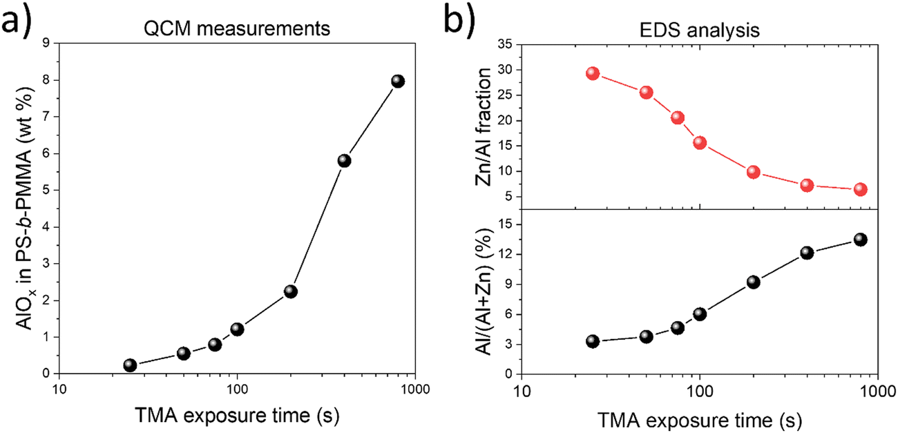 | ||
| Fig. 2 (a) Variation of the AlOx mass gain fraction of AZO infiltrated PS-b-PMMA with respect to the TMA exposure duration. (b) Plot of the atomic composition of Al and the atomic ratio of the Zn/Al in AZO nanostructures for different TMA exposure times. Here, the Al atomic composition within AZO is Al at%/(Al at% + Zn at%) × 100, where respective atomic concentrations of Al and Zn were obtained from the EDS analysis that included Al, Zn, O, and Si (i.e., from the substrate) as the elements of interest (Table S1, ESI†). | ||
We propose that the incorporation of DEZ into PS-b-PMMA is governed by the availability of binding sites (e.g., hydroxyl groups) resulting from alumina priming that can interact with DEZ. Previous studies have shown that during alumina VPI, TMA forms a Lewis adduct—a noncovalent attractive interaction—with the C![[double bond, length as m-dash]](https://www.rsc.org/images/entities/char_e001.gif) O bond of the ester carbonyl in PMMA, particularly when the reaction temperature is below 100 °C.44–46 Over time, the adduct can convert to a C–O–Al covalent bond, with the Al atom bound to PMMA terminated with two methyl groups that eventually become hydroxyl groups—binding sites for DEZ during the following ZnO infiltration cycles.46 Meanwhile, due to the reversibility of the Lewis adduct, TMA can disassemble from the CO bond in PMMA,47 which would make all three methyl groups of TMA available for reaction with water during the next half cycle, producing three hydroxyl groups that can react with DEZ during the following ZnO infiltration. Consequently, the number of hydroxyl groups generated during alumina priming will be dependent on the extent of the reaction between TMA and PMMA during the first half of the alumina priming cycle.
O bond of the ester carbonyl in PMMA, particularly when the reaction temperature is below 100 °C.44–46 Over time, the adduct can convert to a C–O–Al covalent bond, with the Al atom bound to PMMA terminated with two methyl groups that eventually become hydroxyl groups—binding sites for DEZ during the following ZnO infiltration cycles.46 Meanwhile, due to the reversibility of the Lewis adduct, TMA can disassemble from the CO bond in PMMA,47 which would make all three methyl groups of TMA available for reaction with water during the next half cycle, producing three hydroxyl groups that can react with DEZ during the following ZnO infiltration. Consequently, the number of hydroxyl groups generated during alumina priming will be dependent on the extent of the reaction between TMA and PMMA during the first half of the alumina priming cycle.
Assuming the formation of reversible adducts between TMA and carbonyl groups of PMMA, subsequent generation of a maximum of three hydroxyl groups per TMA, a 100% reaction yield of DEZ with hydroxyl groups, and a linear chain growth of ZnO, the maximum number of zinc atoms added after six cycles of ZnO infiltration following alumina priming should be ideally 18 per aluminum atom—i.e., six times the maximum number of hydroxyl groups produced per aluminum atom (i.e., three) during alumina priming. However, this zinc-to-aluminum atomic ratio can be over 18 if the DEZ incorporation into PMMA can also occur via a different route, not involving hydroxyl groups generated from alumina priming, such as the direct coordination/bonding of DEZ with available CO groups in PMMA, which is possible despite its much weaker interaction compared to the TMA case.
Indeed, in our data, when the TMA exposure time is 25 s, the observed number of zinc atoms per aluminum atom is approximately 29, which potentially can be explained by the presence of unreacted carbonyl groups in PMMA after the alumina priming cycle (due to the short TMA exposure time and insufficient amount of incorporated TMA) that can directly interact with DEZ. However, as the exposure duration increases beyond 100 s, we find that the zinc-to-aluminum atomic ratio decreases below 18. This occurs most likely because the extended TMA exposure durations to PS-b-PMMA allows for more time for the conversion of the adducts formed between TMA and CO bonds in PMMA to more stable covalent bonding, which would reduce the maximum number of hydroxyl groups per aluminum atom available for reaction with DEZ during the following ZnO infiltration to two, thereby diminishing the amount of ZnO infiltration per cycle. Therefore, excessive TMA exposure times are likely to induce the formation of Al-rich molecular structures rather than providing additional sites for ZnO growth.
Cross-sectional bright-field TEM was employed for structural analysis of the AZO synthesized with various TMA exposure times (Fig. 3). The low-magnification TEM micrographs (left column) revealed that the AZO nanostructures changed from rounded granular and less periodic at a TMA exposure time of 25 s, to having a rectangular cross-section with a more regular arrangement at 100 s, resembling the lamellar morphology of the PMMA domains in the starting PS-b-PMMA thin film template. A subsequent increase in the TMA exposure time of up to 800 s did not induce significant alterations in the nanostructures, suggesting that the amount of AlOx reacting with the PMMA eventually reaches saturation, resulting in evenly distributed nucleation sites of ZnO within the PMMA domains. The fast Fourier transform (FFT) of the high-resolution TEM images (Fig. 3, middle column), which clearly displays atomic lattices, features diffraction spots randomly oriented along the azimuthal angle (i.e., resembling the diffraction ring), revealing the highly polycrystalline structure. This pattern was consistent across TMA exposure times of 100 s or less. This suggests that the thermal annealing process triggered the crystallization of AZO. Meanwhile, extending the TMA exposure duration to 800 s appears to result in amorphous regions locally, evidenced by a broad scattering ring in the FFT pattern. Low-magnification EDS mapping (Fig. 3, right column) also reveals sporadic Al-enriched regions, potentially associated with locally amorphous Al2O3. These results indicate the formation of either amorphous AZO or Al2O3 due to excessive aluminum that can induce lattice distortion in ZnO, leading to a reduction in crystallinity.48 Overall, the results demonstrated that the TMA exposure time is a crucial factor in controlling AZO growth, morphology, and crystallinity.
 | ||
| Fig. 3 Cross-sectional bright-field TEM micrographs (left: low-magnification and middle: high-resolution, with the inset showing FFT patterns), and HAADF micrographs and EDS elemental mapping images (right) for AZO nanostructures with different TMA exposure times; (a) 25 s, (b) 100 s, and (c) 800 s. All scale bars denote 20 nm, unless specified otherwise. | ||
Aluminum doping is a well-established method for improving the electrical conductivity of zinc oxide nanostructures, thereby rendering them suitable for electroactive device applications.49,50 However, alumina, as an electrical insulator, can have unintended and detrimental effects on the electrical conductivity of nanostructures, and especially detailed studies on the electrical properties of infiltration-synthesized AZO nanostructures derived from BCP have not been performed. To gain a better understanding of the effect of aluminum addition on the conductivity of AZO nanostructures, we investigated the electrical properties of infiltration-synthesized AZO nanowires produced with different TMA exposure times using the transfer length method (TLM). In the TLM method, electrodes with varying channel lengths are intentionally fabricated, such that resistance vs. channel length data can be acquired. The analysis of these data can provide the resistivity of the channel layer from the slope of the plot as described in the subsequent discussion.
Two-terminal I–V measurements were conducted to determine the total resistance of AZO nanowires. The TLM devices consisting of six electrode contacts with five channel lengths (Lch) (5, 8, 10, 15, and 25 μm) were fabricated onto AZO nanowires (Fig. 4(a) and (b)). The conductance of AZO nanostructures was found to improve as the TLM channel length decreased (Fig. S4, ESI†). The representative I–V curves taken from the 5 μm channel length AZO device with different TMA exposure times ranging from 25 to 400 s are shown in Fig. 4(c). Increasing the TMA exposure time from 25 s to 100 s resulted in a markedly enhanced total current from an initial value of 1.4 nA to 13.6 nA at 1 V. However, a further increase in the TMA exposure time to 200 s and 400 s led to a decrease in current to 0.8 nA and 0.03 nA, respectively, at 1 V. After a further increase in the TMA exposure time to 800 s produced a highly resistive state, such that the current was below the detection limit of the instrument.
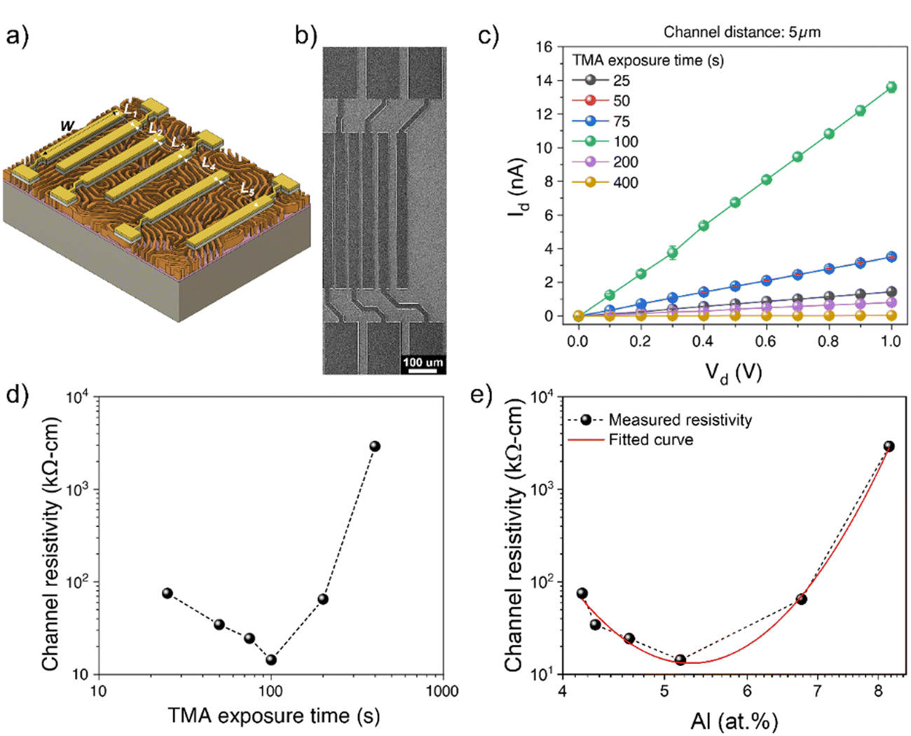 | ||
| Fig. 4 (a) Schematic depiction of TLM electrodes onto AZO nanowires; contact spacing of electrodes are L1: 5 μm, L2: 8 μm, L3: 10 μm, L4: 15 μm, and L5 25 μm. (b) Top-view SEM micrographs of the fabricated AZO nanostructured TLM devices. (c) Representative I–V plots of TLM devices with 5 μm of channel length of AZO nanowires with varying TMA exposure times (25, 50, 75, 100, 200, and 400 s). (d) Channel resistivity of AZO nanostructures with varying TMA exposure times, and (e) evolution of the channel resistivity of AZO nanostructures with varying Al atomic percentages. | ||
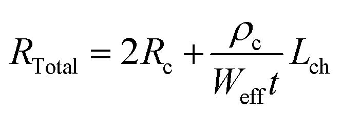
TLM structured electrodes offer a range of channel lengths to allow the extraction of channel resistivity (ρc) and contact resistance (Rc) of AZO nanostructures, thereby studying the evolution of the AZO nanowire channel resistivity with respect to the TMA exposure time. The total resistance of the nanostructures in each TLM device was determined via the slope of the linear region of the I–V curves, as per Ohm's law, which is a function of both the contact resistance and the channel resistivity:
The observed changes in the electrical performance of the infiltration synthesized AZO nanowires can be attributed to the changes in the chemical state that occur due to differences in the TMA exposure time. To further understand these changes, XPS was carried out over AZO nanopatterns synthesized with different TMA exposure durations (Fig. 5), and this revealed that the defects and chemical states of the elements present in the AZO nanostructure were affected by the TMA infiltration time. All the XPS peaks were calibrated by taking C 1s references at 284.8 eV to compensate for any charge induced shifts. The deconvoluted XPS spectra of C 1s, O 1s, Zn 2p, and Al 2p peaks for varying TMA exposure times of infiltration-synthesized AZO nanostructures are shown in Fig. S6–S9 (ESI†), respectively.
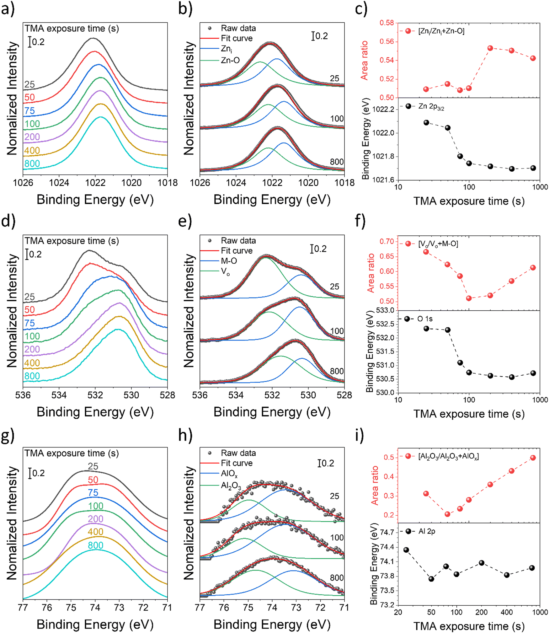 | ||
| Fig. 5 (a), (d) and (g) XPS spectra of Zn 2p3/2, O 1s, and Al 2p peaks of AZO nanostructures as a function of the TMA exposure time, respectively. (b), (e) and (f) Zn 2p3/2, O 1s, and Al 2p XPS spectra of selected AZO nanostructures with varying TMA exposure times (25, 100, and 800 s), respectively. (c), (f) and (i) Plot of the peak positions (bottoms) and the ratio of the peak area (top) of Zn 2p3/2, O 1s, and Al 2p, respectively. | ||
The XPS spectra of Zn 2p exhibit two characteristic peaks at 1044.5 eV and 1021.5 eV, belonging to Zn 2p1/2 and 2p3/2, respectively. The binding energy of the Zn 2p3/2 peak shifted to a lower binding energy as the TMA exposure time increased (Fig. 5(a)), and it was observed that the core level decreased rapidly by 0.35 eV from 1022.09 eV to 1021.74 eV for an increase in the TMA exposure time from 25 s to 100 s. Thereafter the peak shift saturated at 1021.7 eV for a TMA exposure time of 800 s by only decreasing 0.04 eV (Fig. 5(c)). The observed core level shift corresponds to charge transfer under the chemical bond between Al and Zn, where Al tends to donate electrons to Zn due to the electronegativity difference.58 The results suggest that the channel resistivity decreases due to the increase in the carrier concentration by the Al doping effect, and that the doping effect remains almost the same from the TMA exposure time of 100 s or more.
To gain a deeper insight into zinc-related defects, the Zn 2p3/2 peak was deconvoluted into two components-zinc interstitials (Zni) at 1021.7 eV and zinc bonded to oxygen in the ZnO matrix (Zn–O) at 1022.6 eV – for quantitative analysis (Fig. 5(b)). In Fig. 5(c), the peak area fraction of zinc interstitials (Zni/Zni + Zn–O) increased from 50.9% to 54.2% as the TMA exposure duration increased, indicating an increase in zinc interstitial defects. Interestingly, there appears to be almost a step change in the fraction of zinc interstitials from a TMA exposure time of 100 s to 200 s. The Zn defects might migrate to the grain boundaries and increase grain boundary potentials, resulting in relatively high channel resistivity in the AZO nanostructures synthesized with a longer TMA exposure time, which have defect-rich states. The result also agrees with AZO nanostructures exhibiting minimum resistivity at a TMA exposure time of 100 s, which corresponds to 5.2 at% of Al (Fig. 4(d) and (e)).
In Fig. 5(d), the O 1s peak is located at 532.3 eV for a TMA exposure time of 25 s, and as the TMA exposure time increases, the peak position shifts to a lower binding energy of 530.7 eV. The binding energy of the O 1s peaks was deconvoluted into two peaks centered at 530.4 eV and 532.3 eV, which were denoted as M–O and Vo, respectively. M–O (530.4 eV) is associated with O2− ions in the wurtzite structure of the hexagonal Zn2+ ion array, which are surrounded by zinc atoms with the full supplement of the nearest neighbor O2− ions.59 Vo (532.3 eV) is associated with O2− ions located in the oxygen deficient regions of lattice (point defect), and its intensity is affected by the concentration of oxygen vacancies (Fig. 5(e)).40,60 To ascribe the quantitative information about oxygen vacancies, the Vo/Vo + M–O ratio was calculated from the area under the respective peaks and is shown in Fig. 5(f). The increase in the TMA exposure time from 25 to 100 s led to a reduction in the oxygen vacancy ratio from 66.6 to 51.1%, followed by an increase to 61.3% for TMA exposure times beyond 100 s.
The observed initial reduction and the following increase of the amount of Vo point defects with an increase in the TMA exposure time likely result from a commensurate change in AZO crystallinity. It has been observed by several prior studies that AZO crystallinity increases at the optimal aluminum doping concentration, but it decreases with additional doping.61–63 One potential origin of the increased crystallinity is the disturbed charge neutrality by the substitution of Zn2+ with Al3+, which can enhance crystal growth along a particular orientation.64 Beyond the optimal Al doping centration, additional aluminum atoms that have smaller atomic radii are now expected to rather cause a disturbed crystallinity due to lattice distortion, making them even amorphous.62 Additionally, they cannot further substitute lattice zinc atoms due to the solubility limit, causing the formation of phase-separated AlOx regions, which not only further disrupt AZO crystallinity but also decrease AZO conductivity. Accordingly, AZO nanostructures with a TMA exposure time of 100 s exhibit the lowest values for both the Vo/Vo + M–O ratio (Fig. 5(f)) and the channel resistivity (Fig. 4(d)). Consistently, XPS data further confirm an increase in the alumina content in the AZO nanostructure with an increase in the TMA exposure duration. The XPS spectra of Al 2p (Fig. 5(g)) were divided into two peaks centered at 73.4 eV and 74.9 eV (Fig. 5(h)), which can be attributed to non-stoichiometric AlOx (Al–O–Zn) and stoichiometric Al2O3 bonding, respectively. The overall spectral area for Al 2p was increased along with an increase of the TMA exposure time corresponding to the elevated Al content. Furthermore, the spectral area fraction of stoichiometric Al2O3 (Al2O3/Al2O3 + AlOx) increased along with an increase in the TMA exposure time (Fig. 5(i)). Overall, the increased alumina fraction within AZO will act as charge scattering centers, thus diminishing the electrical conductivity.
Conclusions
In summary, we have explored the effect of alumina priming on infiltration synthesized AZO nanostructures, fabricated using a self-assembled PS-b-PMMA thin film by manipulating the TMA exposure time in the alumina priming process. The synthesized AZO nanostructures feature the facile tunability of characteristic dimensions, chemical composition, and electrical conductivity by controlling the duration of TMA exposure in the alumina priming process. Specifically, increasing the TMA exposure time led to the improved ZnO infiltration fidelity as well as an increase in the feature dimensions (width and height of nanowires) of the resulting AZO nanostructure, accompanied by an increase in the Al content. As the TMA exposure duration increased, the zinc-to-aluminum ratio of the AZO structure decreased, and after 400 s, the ratio decreased to less than 18:1. This observation implies that while TMA exposure enables the formation of ZnO seeding sites, excessive TMA exposure contributes to the formation of aluminum oxide clusters. On the other hand, the electrical resistivity of AZO nanowires was initially reduced down to 14.3 kΩ cm with an increase in the TMA exposure time of up to 100 s, with a corresponding Al concentration of 6.02%, while a further increased TMA exposure duration rendered a steep (up to two orders of magnitude) increase in the resistivity. The origin of the decline in the electrical conductivity of AZO nanostructures exposed to TMA for an extended period was attributed to an increase in the defect concentration with accompanying XPS studies. As the defects migrate toward grain boundaries, enhancing the grain boundary potential increased electron scattering, resulting in a reduction in the carrier electron mobility and a consequent increase in AZO resistivity. The demonstrated results elucidate the effect of alumina-priming on the chemical, structural and electrical properties of the infiltration-synthesized AZO nanostructures and provide a guideline for developing advanced VPI-derived functional nanostructures with tailored properties.
Author contributions
W.-I. L.: conceptualization, data curation, formal analysis, investigation, methodology, visualization, writing original draft, and writing – review and editing. A. S.: conceptualization, investigation, and methodology. K. K.: investigation and methodology. N. T.: conceptualization, investigation, validation, and writing – review & editing, C.-Y. N.: conceptualization, funding acquisition, investigation, project administration, resources, supervision, validation, and writing – review & editing.Conflicts of interest
There are no conflicts to declare.Acknowledgements
This research was performed at the Center for Functional Nanomaterials (CFN) which is a U.S. Department of Energy Office of Science User Facility at Brookhaven National Laboratory (BNL) under contract no. DE-SC0012704. This work used Materials Synthesis & Characterization, Nanofabrication, Advanced UV and X-ray Probes, and Electron Microscopy facilities at the CFN. The authors thank Dr Xiao Tong for providing assistance with XPS characterization.References
- R. F. Service, Science, 2018, 361, 321 CrossRef PubMed.
- P. W. Majewski and K. G. Yager, J. Phys.: Condens. Matter, 2016, 28, 403002 CrossRef PubMed.
- S. Darling, Prog. Polym. Sci., 2007, 32, 1152–1204 CrossRef CAS.
- C. T. Black, R. Ruiz, G. Breyta, J. Y. Cheng, M. E. Colburn, K. W. Guarini, H.-C. Kim and Y. Zhang, IBM J. Res. Dev., 2007, 51, 605–633 CAS.
- A. Subramanian, N. Tiwale and C.-Y. Nam, JOM, 2019, 71, 185–196 CrossRef.
- R. A. Segalman, Mater. Sci. Eng., R, 2005, 48, 191–226 CrossRef.
- S. H. Mir, L. A. Nagahara, T. Thundat, P. Mokarian-Tabari, H. Furukawa and A. Khosla, J. Electrochem. Soc., 2018, 165, B3137–B3156 CrossRef CAS.
- A. Subramanian, N. Tiwale, W.-I. Lee and C.-Y. Nam, Front. Nanotechnol., 2021, 94 Search PubMed.
- K. W. Gotrik and C. Ross, Nano Lett., 2013, 13, 5117–5122 CrossRef CAS PubMed.
- S. H. Kim, M. J. Misner, T. Xu, M. Kimura and T. P. Russell, Adv. Mater., 2004, 16, 226–231 CrossRef CAS.
- A. Modi, S. M. Bhaway, B. D. Vogt, J. F. Douglas, A. Al-Enizi, A. Elzatahry, A. Sharma and A. Karim, ACS Appl. Mater. Interfaces, 2015, 7, 21639–21645 CrossRef CAS PubMed.
- A. Subramanian, G. Doerk, K. Kisslinger, H. Y. Daniel, R. B. Grubbs and C.-Y. Nam, Nanoscale, 2019, 11, 9533–9546 RSC.
- D. H. Yi, C.-Y. Nam, G. Doerk, C. T. Black and R. B. Grubbs, ACS Appl. Polym. Mater., 2019, 1, 672–683 CrossRef CAS.
- M. Park, P. Chaikin, R. A. Register and D. H. Adamson, Appl. Phys. Lett., 2001, 79, 257–259 CrossRef CAS.
- M. Park, C. Harrison, P. M. Chaikin, R. A. Register and D. H. Adamson, Science, 1997, 276, 1401–1404 CrossRef CAS.
- A. Subramanian, N. Tiwale, G. Doerk, K. Kisslinger and C.-Y. Nam, ACS Appl. Mater. Interfaces, 2019, 12, 1444–1453 CrossRef PubMed.
- A. E. Paiva, J. F. B. Vasquez, T. S. Perova, F. G. M. Borsagli and M. Morris, Mater. Lett., 2022, 313, 131682 CrossRef CAS.
- J. Chai and J. M. Buriak, ACS Nano, 2008, 2, 489–501 CrossRef CAS PubMed.
- Q. Peng, Y. C. Tseng, S. B. Darling and J. W. Elam, Adv. Mater., 2010, 22, 5129–5133 CrossRef CAS PubMed.
- A. Checco, A. Rahman and C. T. Black, Adv. Mater., 2014, 26, 886–891 CrossRef CAS PubMed.
- C.-Y. Nam, A. Stein and K. Kisslinger, J. Vac. Sci. Technol., B: Nanotechnol. Microelectron.: Mater., Process., Meas., Phenom., 2015, 33, 06F201 Search PubMed.
- C.-Y. Nam, A. Stein, K. Kisslinger and C. T. Black, Appl. Phys. Lett., 2015, 107, 203106 CrossRef.
- G. N. Parsons, S. E. Atanasov, E. C. Dandley, C. K. Devine, B. Gong, J. S. Jur, K. Lee, C. J. Oldham, Q. Peng and J. C. Spagnola, Coord. Chem. Rev., 2013, 257, 3323–3331 CrossRef CAS.
- P. G. Mani-Gonzalez, C. McFeely, M. Snelgrove, K. Shiel, J. A. Hernandez Marquez and R. O’Connor, J. Vac. Sci. Technol., A, 2021, 39, 040403 CrossRef CAS.
- L. Mai, D. Maniar, F. Zysk, J. Schöbel, T. D. Kühne, K. Loos and A. Devi, Dalton Trans., 2022, 51, 1384–1394 RSC.
- E. K. McGuinness, C. Z. Leng and M. D. Losego, ACS Appl. Polym. Mater., 2020, 2, 1335–1344 CrossRef CAS.
- A. Motta, G. Seguini, M. Perego, R. Consonni, A. C. Boccia, G. Ambrosio, C. Baratto, P. Cerruti, M. Lavorgna and S. Tagliabue, ACS Appl. Polym. Mater., 2022, 4, 7191–7203 CrossRef CAS PubMed.
- A. Álvarez-Yenes, M. Borraz and M. Knez, Proc. SPIE PC12944, Bioinspiration, Biomimetics, and Bioreplication XIV, PC1294401 DOI:10.1117/12.3014709.
- O. Yurkevich, E. Modin, I. Šarić Janković, R. Peter, M. Petravić and M. Knez, Chem. Mater., 2023, 35, 7529–7541 CrossRef CAS.
- S. Greil, A. Rahman, M. Liu and C. T. Black, Chem. Mater., 2017, 29, 9572–9578 CrossRef CAS.
- D. Pleshek, J. Tran, Y. Li, A. Shirani, E. V. Shevchenko and D. Berman, ACS Appl. Mater. Interfaces, 2021, 13, 35941–35948 CrossRef CAS PubMed.
- Y. Yu, Z. Li, Y. Wang, S. Gong and X. Wang, Adv. Mater., 2015, 27, 4938–4944 CrossRef CAS PubMed.
- A. Rahman, A. Ashraf, H. Xin, X. Tong, P. Sutter, M. D. Eisaman and C. T. Black, Nat. Commun., 2015, 6, 5963 CrossRef CAS PubMed.
- X. Ye, J. Kestell, K. Kisslinger, M. Liu, R. B. Grubbs, J. A. Boscoboinik and C.-Y. Nam, Chem. Mater., 2017, 29, 4535–4545 CrossRef CAS.
- J. Kamcev, D. S. Germack, D. Nykypanchuk, R. B. Grubbs, C.-Y. Nam and C. T. Black, ACS Nano, 2013, 7, 339–346 CrossRef CAS PubMed.
- R. P. Padbury and J. S. Jur, Langmuir, 2014, 30, 9228–9238 CrossRef CAS PubMed.
- H. I. Akyildiz, R. P. Padbury, G. N. Parsons and J. S. Jur, Langmuir, 2012, 28, 15697–15704 CrossRef CAS PubMed.
- J. W. Elam, M. Biswas, S. Darling, A. Yanguas-Gil, J. D. Emery, A. B. Martinson, P. F. Nealey, T. Segal-Peretz, Q. Peng and J. Winterstein, ECS Trans., 2015, 69, 147 CrossRef CAS PubMed.
- Q. Peng, Y.-C. Tseng, S. B. Darling and J. W. Elam, ACS Nano, 2011, 5, 4600–4606 CrossRef CAS PubMed.
- L. E. Ocola, A. Connolly, D. J. Gosztola, R. D. Schaller and A. Yanguas-Gil, J. Phys. Chem. C, 2017, 121, 1893–1903 CrossRef CAS.
- G. Luka, T. Krajewski, B. Witkowski, G. Wisz, I. Virt, E. Guziewicz and M. Godlewski, J. Mater. Sci.: Mater. Electron., 2011, 22, 1810–1815 CrossRef CAS.
- H. Kim, C. Gilmore, J. Horwitz, A. Pique, H. Murata, G. Kushto, R. Schlaf, Z. Kafafi and D. Chrisey, Appl. Phys. Lett., 2000, 76, 259–261 CrossRef CAS.
- A. S. Nikhil Tiwale, X. Qu, G. Freychet, E. Gann, K. Kisslinger and C.-Y. Nam, under review.
- G. T. Hill, D. T. Lee, P. S. Williams, C. D. Needham, E. C. Dandley, C. J. Oldham and G. N. Parsons, J. Phys. Chem. C, 2019, 123, 16146–16152 CrossRef CAS.
- E. C. Dandley, C. D. Needham, P. S. Williams, A. H. Brozena, C. J. Oldham and G. N. Parsons, J. Mater. Chem. C, 2014, 2, 9416–9424 RSC.
- M. Biswas, J. A. Libera, S. B. Darling and J. W. Elam, Chem. Mater., 2014, 26, 6135–6141 CrossRef CAS.
- R. Z. Waldman, D. J. Mandia, A. Yanguas-Gil, A. B. Martinson, J. W. Elam and S. B. Darling, J. Chem. Phys., 2019, 151, 190901 CrossRef PubMed.
- H. S. Wai and C. Li, Nanomaterials, 2022, 12, 195 CrossRef CAS PubMed.
- X. Jiang, F. Wong, M. Fung and S. Lee, Appl. Phys. Lett., 2003, 83, 1875–1877 CrossRef CAS.
- G. Murdoch, S. Hinds, E. Sargent, S. Tsang, L. Mordoukhovski and Z. Lu, Appl. Phys. Lett., 2009, 94, 138 CrossRef.
- C. Y. Nam and A. Stein, Adv. Opt. Mater., 2017, 5, 1700807 CrossRef.
- Z. Starowicz, A. Zięba, J. Ostapko, M. Wlazło, G. Kołodziej, M. J. Szczerba, G. Putynkowski and R. P. Socha, Mater. Sci. Eng., B, 2023, 292, 116405 CrossRef CAS.
- E. Shkondin, O. Takayama, M. A. Panah, P. Liu, P. V. Larsen, M. D. Mar, F. Jensen and A. Lavrinenko, Opt. Mater. Express, 2017, 7, 1606–1627 CrossRef CAS.
- Y. Li, R. Yao, H. Wang, X. Wu, J. Wu, X. Wu and W. Qin, ACS Appl. Mater. Interfaces, 2017, 9, 11711–11720 CrossRef CAS PubMed.
- N. Van Toan, T. T. K. Tuoi, N. Inomata, M. Toda and T. Ono, Sci. Rep., 2021, 11, 1204 CrossRef CAS PubMed.
- S. Jantrasee, P. Moontragoon and S. Pinitsoontorn, J. Semicond., 2016, 37, 092002 CrossRef.
- Y. Zhang, Y. Yang, J. Zhao, R. Tan, W. Wang, P. Cui and W. Song, J. Mater. Sci., 2011, 46, 774–780 CrossRef CAS.
- S. Bang, S. Lee, Y. Ko, J. Park, S. Shin, H. Seo and H. Jeon, Nanoscale Res. Lett., 2012, 7, 1–11 CrossRef PubMed.
- P.-T. Hsieh, Y.-C. Chen, K.-S. Kao and C.-M. Wang, Appl. Phys. A: Mater. Sci. Process., 2008, 90, 317–321 CrossRef CAS.
- U. Ilyas, R. S. Rawat, T. Tan, P. Lee, R. Chen, H. Sun, L. Fengji and S. Zhang, J. Appl. Phys., 2011, 110, 093522 CrossRef.
- F. Eskandari, M. Ranjbar, P. Kameli and H. Salamati, J. Alloys Compd., 2015, 649, 35–45 CrossRef CAS.
- W. Maeng, J.-w Lee, J. H. Lee, K.-B. Chung and J.-S. Park, J. Phys. D: Appl. Phys., 2011, 44, 445305 CrossRef.
- A. Wang, T. Chen, S. Lu, Z. Wu, Y. Li, H. Chen and Y. Wang, Nanoscale Res. Lett., 2015, 10, 1–10 CrossRef CAS PubMed.
- P. Banerjee, W.-J. Lee, K.-R. Bae, S. B. Lee and G. W. Rubloff, J. Appl. Phys., 2010, 108, 043504 CrossRef.
Footnote |
| † Electronic supplementary information (ESI) available. See DOI: https://doi.org/10.1039/d4ma00346b |
| This journal is © The Royal Society of Chemistry 2024 |