
 Open Access Article
 This Open Access Article is licensed under a Creative Commons Attribution-Non Commercial 3.0 Unported Licence
Insights into the interfaces of VO2(M) and VO2(B) polymorphs with different substrates
Elaheh
Mohebbi
a,
Eleonora
Pavoni
 a,
Luca
Pierantoni
b,
Pierluigi
Stipa
a,
Emiliano
Laudadio
*a and
Davide
Mencarelli
b
a,
Luca
Pierantoni
b,
Pierluigi
Stipa
a,
Emiliano
Laudadio
*a and
Davide
Mencarelli
b
aDepartment of Matter, Environmental Sciences, and Urban Planning, Marche Polytechnic University, 60131 Ancona, Italy. E-mail: e.laudadio@staff.univpm.it
bInformation Engineering Department, Marche Polytechnic University, 60131 Ancona, Italy
First published on 11th March 2024
Abstract
The phenomena arising at the interface between oxide materials and substrates can fundamentally and practically change the physical and chemical properties of the materials themselves. In this study, we employed density functional theory (DFT) calculations to elucidate the stability and optical properties of VO2(M) and VO2(B) interactions with substrates of sapphire(c-cut), sapphire(r-cut), SrTiO3(001), SrTiO3(111), SrNbO3(001), SrNbO3(111), LaAlO3(c-cut), and LaAlO3(r-cut). The surface calculations showed that the fully relaxed SrTiO3(111) and SrNbO3(001) possess the highest energies of 31.8 eV nm−2 and 21.15 eV nm−2 relative to other slabs, before optimizing with VO2(M) and VO2(B) polymorphs, respectively. The calculated adsorption energy indicated that the interface of VO2(M) and VO2(B) structures showed more stability on SrTiO3(001) and SrTiO3(111), with adsorption energy values of 2.83 eV and 0.91 eV, respectively. Furthermore, the optical absorption properties of the highest and lowest stable interfaces have been evaluated. The outcomes predicted that VO2(M)@SrTiO3(001) and VO2(B)@SrTiO3(111) have their optical adsorption in the visible light range, while VO2(M)@sapphire(c-cut) and VO2(B)@sapphire(c-cut) showed the main adsorption peak in the infrared region.
Introduction
Epitaxial synthesis of heterostructure oxides has shown considerable promise in creating new functionalities and chemical–physical properties by controlling some parameters, such as lattice, spin, charge, and orbital order.1 Heterostructures of oxide materials allow for tuning the electronic, magnetic, and optical properties, as well as giving rise to emergent behaviours that are distinct from the bulk properties of either material. Since there are no substrates available with similar structures (lattice parameters and crystal symmetry), the ability to grow the thin films of binary oxides like TiO22 and VO23,4 on lattice- and symmetry-mismatched substrates is of crucial importance for discovering their unprecedented potential.It is well known that vanadium oxides (VO2) represent an abundant and diverse family of compounds with multipurpose applications. VO2 exists in multiform polymorphic stable and metastable forms, including rutile VO2(R),5 monoclinic VO2(M),6 and triclinic VO2(T) phases,7 that are similar in structure. But there are other four VO2 phases designated as tetragonal VO2(A),8 monoclinic VO2(B),9 paramontroseite VO2,10 and VO2 with a new body centered-cubic (bcc) structure.11 Among them, VO2(M) possesses a fully reversible metal–insulator phase transition to the most stable VO2(R), associated with the benefits of huge temperature-induced resistivity changes as well as the selective optical switches, which have received great interest in industrial and scientific areas for construction of intelligent devices such as temperature sensors,12 GHz operating frequency,13 thermochromics,14 and energy efficient smart windows.14 On the other hand, the VO2(B) phase has also been explored as a promising cathode material in Li-ion batteries, not only on the basis of its appropriate electrode potential, but also its particular tunnelled structure.15 However, metastable VO2(B) is a relatively less-studied polymorph in comparison to the other oxides of vanadium.
Recently, our group has carried out a comprehensive DFT-study on the characterization of the geometry, stability, Raman spectra, and the electronic, magnetic, and optical properties of VO2(M)16 and VO2(B)17,18 nanostructures. The study on the electronic band gap of VO2(M)16 based on the Heyd–Scuseria–Ernzerhof (HSE)19 functional showed excellent agreement with photoemission experiments (band gap ∼ 0.6–0.7 eV)20 by a band gap of 0.6 eV. In addition to the improved prediction of the peak position in the absorption spectra with the same functional, this method also described reasonably well the static dielectric constant of 7.54 of VO2(M), showing an excellent match with the experimental values. In an experimental work by Lourembam et al.,21 they have investigated the photoinduced insulator-to-metal transition in VO2(B) using the temperature-dependent optical pump–probe technique. This study reported the metallic phase (300 K) and the insulating phase (100 K) of this structure, respectively; however, the insulating phase can be indicated by two electronic relaxation times and the metallic phase showed only one characteristic time. Our recently study17 based on the use of PBEsol22 demonstrated for the first time the experimental metallic-like phase of VO2(B).
So far, using pulsed laser epitaxy (PLE), high quality VO2(M) and VO2(B) thin films were successfully stabilized on perovskite substrates like SrTiO3. Chen et al.23 reported that the textured VO2(B) thin film with a layered structure was grown on SrTiO3(001) by pulsed laser deposition. In addition, a small amount of the VO2(M) phase can co-grow in the VO2(B) phase. This study indicates an alternative approach to enhance the performance of insulating VO2(B) based batteries by increasing the electrical conductivity. Srivastava et al.24 demonstrated the novel heterostructures of high-quality single-phase films of VO2 (A and B) on the SrTiO3 substrate by controlling the vanadium arrival rate (laser frequency) and oxidation of the V atoms. In addition, the c-plane Al2O3 (sapphire) substrate has been used to consider the first phase transition stability of VO2 thin films grown via both ex situ heating and in situ heating by transmission electron microscopy (TEM). Electrical resistance measurements were conducted on the VO2 thin films to characterize the semiconductor to metallic transition (SMT) properties during multiple thermal cycles. In situ TEM heating experiments were conducted to investigate the film microstructure evolutions during phase transition cycles.25
In this work, using DFT calculations, for the first time, we reported the stability and optical properties of different interfaces of VO2(M) and VO2(B) on sapphire(c-cut), sapphire(r-cut), SrTiO3(001), SrTiO3(111), Nb substituted with Ti in SrNbO3(001) and SrNbO3(111), LaAlO3(c-cut), and LaAlO3(r-cut) surfaces and used these results to understand how two dissimilar materials can form heterostructures with different characterizations. Computational advances in the atomic-scale simulations of oxide heterostructures are able to provide a fertile new ground for creating novel states at their interfaces and varied symmetry constraints can be used to design structures exhibiting phenomena that are not found in the bulk constituents and then that can be exploitable in practical device applications of VO2.
Results and discussion
Initially, the slab of various configurations was modelled; then, different interfaces, as seen in Fig. 1, were constructed by the interactions between the slabs and the VO2(M) and VO2(B) perpendicular to the surface along the z direction. All the information related to the crystal structure and lattice parameters for substrates of Al2O3, SrTiO3 and LaAlO3 as well as VO2(M and B) polymorphs are reported in Table 1. Moreover, the details related to the lattice dimensions for different interfaces are reported in Table 2. It is evident from our computational results that after the structural relaxation of all supercells, the vertical distances between VO2 (M and B) and different facets of SrTiO3 and SrNbO3 are lower (an average interface distance of 2.37 Å) than those for Al2O3 and LaAlO3 substrates. The outcomes indicate that the adsorption is primarily dominated by the vdW interactions on the substrates of sapphire facets and even in La-containing slabs, with vertical distances around 3.63 Å. By considering the chemical properties of different elements like electron configuration, atomic radius and electronegativity, as shown in Table 3, since the vanadium (V) atom has a small atomic radius of 134 pm and an electronegativity of 1.63, the charges can transfer more easily with strontium (Sr), having an electronegativity of 0.91 and a bigger radius sphere of 255 pm, compared to aluminium (Al) with a similar electronegativity of 1.61 and an atomic radius of 1.43. When we used the SrNbO3 and LaAlO3 substrates, still we get the direct connections of Sr–V and Al–V in the interfaces, and the chemical properties of Nb and La atoms could not significantly affect the chemical properties of vanadium atoms. The comparison between titanium (Ti) (niobium (Nb)) in SrTiO3 (SrNbO3) substrates indicates that the charges can transfer more easily with titanium (Ti), having an electronegativity of 1.54 and a smaller radius sphere of 187 pm, compared to Nb with a similar electronegativity of 1.60 but a bigger atomic radius of 207 pm. The same condition exists for the La atom in LaAlO3 which has a bigger atomic radius (250 pm) than Al (143 pm). However, as we see later, the presence of these elements can influence less the stability of heterostructures. | ||
| Fig. 1 Schematic representations of VO2(M) and VO2(B) material interfaces with different substrates. The color code in the ball and stick models: V grey, O red, Al pink, Sr green, Nb cyan, Ti silver, and La light blue. | ||
| Bulk systems | Crystal structure (space group) | Lattice constant | |||
|---|---|---|---|---|---|
| a (Å) | b (Å) | c (Å) | β (°) | ||
| Al2O3 | Trigonal (R![[3 with combining macron]](https://www.rsc.org/images/entities/char_0033_0304.gif) C) C) |
4.81 | 4.81 | 13.12 | 120 |
| SrTiO3 | Cubic (Pmm) |
3.95 | 3.95 | 3.95 | 90 |
| LaAlO3 | Trigonal (RC) |
5.41 | 5.41 | 13.19 | 120 |
| VO2(M) | Monoclinic (P21/c) | 5.38 | 4.52 | 5.74 | 122.6 |
| VO2(B) | Monoclinic (C2/m) | 12.03 | 3.69 | 6.42 | 106 |
| Interface | a (Å) | b (Å) | c (Å) | β (°) |
|---|---|---|---|---|
| VO2(M)@sapphire(c-cut) | 9.61 | 10.35 | 21.61 | 62.35 |
| VO2(M)@sapphire(r-cut) | 18.34 | 7.06 | 21.07 | 118.11 |
| VO2(M)@SrTiO3(001) | 11.15 | 7.89 | 23.29 | 45 |
| VO2(M)@SrTiO3(111) | 11.15 | 11.15 | 22.27 | 60 |
| VO2(M)@SrNbO3(001) | 11.15 | 7.89 | 20.27 | 45 |
| VO2(M)@SrNbO3(111) | 11.15 | 11.15 | 24.07 | 60 |
| VO2(M)@LaAlO3(c-cut) | 10.82 | 10.78 | 22.62 | 120.112 |
| VO2(M)@LaAlO3(r-cut) | 23.55 | 5.39 | 22.31 | 90.26 |
| VO2(B)@sapphire(c-cut) | 17.35 | 11.06 | 20.01 | 15.25 |
| VO2(B)@sapphire(r-cut) | 16.94 | 7.71 | 22.30 | 95.36 |
| VO2(B)@SrTiO3(001) | 11.83 | 7.89 | 18.39 | 90 |
| VO2(B)@SrTiO3(111) | 12.51 | 11.15 | 19.43 | 120 |
| VO2(B)@SrNbO3(001) | 11.83 | 7.89 | 28.92 | 90 |
| VO2(B)@SrNbO3(111) | 11.15 | 11.15 | 19.07 | 120 |
| VO2(B)@LaAlO3(c-cut) | 10.82 | 10.78 | 17.42 | 59.88 |
| VO2(B)@LaAlO3(r-cut) | 17.85 | 10.78 | 16.87 | 41.24 |
| Element | Electron configuration | Atomic radius (pm) | Electronegativity |
|---|---|---|---|
| Sr(Ti, Nb)O3 | |||
| Sr | [Kr] 5s2 | 255 | 0.95 |
| Ti | [Ar] 3d24s2 | 187 | 1.54 |
| Nb | [Kr] 4d45s1 | 207 | 1.60 |
| Al(Al, La)O3 | |||
| Al | [Ne] 3s23p1 | 143 | 1.61 |
| La | [Xe] 5d16s2 | 250 | 1.10 |
| VO2 | |||
| V | [Ar] 3d34s2 | 134 | 1.63 |
After simulating all interface systems, we removed VO2(M) and VO2(B) polymorphs from the supercells and we evaluated the surface energy of different relaxed surfaces. The theoretical formalism for evaluating the surface energy can be expressed from the following formula:26
| Es = E(n) + nEBulk/2A | (1) |
 | ||
| Fig. 2 Surface energy for relaxed different slabs of sapphire(c-cut), sapphire(r-cut), SrTiO3(001), SrTiO3(111), SrNbO3(001), SrNbO3(111), LaAlO3(c-cut), and LaAlO3(r-cut) before optimizing with VO2(M) (A) and VO2(B) (B) polymorphs. | ||
As can be seen, in the case of VO2(M), the surface energy of fully relaxed SrTiO3(111) is considerably larger than all the slabs with 31.8 eV nm−2; however, the surface energy of sapphire(c-plane) has a similar magnitude to those of sapphire(r-plane), SrNbO3(111), and SrTiO3(001) by values of 15.65 eV nm−2, 15.63 eV nm−2, 14.98 eV nm−2, and 14.86 eV nm−2, respectively. The magnitude of the relaxed surface energies for SrNbO3(001) is lower than that for all the slabs with 7.22 eV nm−2 and some middle surface energy values can be observed for LaAlO3(c-cut) (13.61 eV nm−2) and LaAlO3(r-cut) (13.03 eV nm−2). Inspections of Fig. 2 show that the surface energy of different interfaces with the VO2(B) polymorph assumed different values, in the order of SrNbO3(001) > SrTiO3(001) > sapphire(r-cut) > SrNbO3(111) > LaAlO3(c-cut) > SrTiO3(111) > sapphire(c-cut) > LaAlO3(c-cut) with the surface energies of 21.15 > 20.94 > 16.19 > 15.79 > 13.68 > 12.34 > 12.21> 9.23 eV nm−2, respectively. Woo et al.27 also concluded the surface energy of 28–34 eV nm−2 of SrTiO3(111) as the most stable facet of SrTiO3. In fact, there is also reasonably good qualitative agreement with the theoretical results of Stirner et al.28 who obtain the relative surface energies of various sapphire surfaces with the ratios of 11–30 eV nm−2 for the c-plane and 14–19 eV nm−2 for the r-plane. It is also interesting to note from Fig. 2 that, amongst these different surface facets, r- and c-plane LaAlO3 have shown the middle surface energy in good consistency with that shown in ref. 29 in which the surface energy of 5–29 eV nm−2 is reported for the c-plane face of this substrate.
To find the most stable geometric configurations, we investigated the adsorption energy of VO2(M) and VO2(B) on different surfaces (Fig. 3). We calculated the adsorption of different interfaces using the following eqn (2)30,31
| Eads = EVO2(x) + Esubstrate − EVO2(x)+substrate | (2) |
 | ||
| Fig. 3 Adsorption energy for different interfaces of VO2(M and B) polymorphs on sapphire(c-cut), sapphire(r-cut), SrTiO3(001), SrTiO3(111), SrNbO3(001), SrNbO3(111), LaAlO3(c-cut), and LaAlO3(r-cut) substrates. | ||
Optical properties
The absorption coefficients for VO2(M) and VO2(B) polymorphs on the VO2(M)@sapphire(c-cut), VO2(M)@SrTiO3(001), VO2(B)@sapphire(c-cut), and VO2(B)@SrTiO3(111) interfaces are plotted in Fig. 4, as the most (VO2(M)@SrTiO3(001) and VO2(B)@SrTiO3(111)) and less (VO2(M)@sapphire(c-cut) and VO2(B)@sapphire(c-cut)) stable interfaces, as we discussed before. Here, we reported the acquired results in the visible (from 380 to 780 nm) and infrared (from 780 to 2500 nm) ranges as a function of wavelength. Based on this figure and the range of photon energy, the maximum absorption coefficients are 28 × 104 cm−1 (at 500 nm) and 21 × 104 cm−1 (at 620 nm) for VO2(M)@SrTiO3(001) and VO2(B)@SrTiO3(111) along the xx in-plane direction in the central energy zone of visible light (green–yellow) and low energy part of the visible light (red), respectively. The corresponding values predicted for VO2(M)@sapphire(c-cut) and VO2(B)@sapphire(c-cut) are 24 × 104 cm−1 (at 1500 nm) and 19 × 104 cm−1 (at 1000 nm), along the in-plane direction, respectively, with the first main peaks of the absorption coefficient in the light infrared region of the electromagnetic spectrum. | ||
| Fig. 4 Optical adsorption of VO2(M)@sapphire(c-cut) (A), VO2(M)@SrTiO3(001) (B), VO2(B)@sapphire(c-cut) (C), and VO2(B)@SrTiO3(111) (D) interfaces, as a function of the wavelength (nm) scale. | ||
We next discuss the dielectric constant of the four interfaces, as we assessed their optical adsorption. The real and imaginary parts of dielectric constant of VO2(M)@sapphire(c-cut)(A), VO2(M)@SrTiO3(001)(B), VO2(B)@sapphire(c-cut)(C), and VO2(B)@SrTiO3(111) (D) interfaces are presented in Fig. 5, as a function of energy (eV). The imaginary part of all interfaces began with a high intensity of VO2(M)@sapphire(c-cut) (A), while the intensity of peaks dropped with that of VO2(B)@SrTiO3(111) (D). In addition, the optical edge, which is called the optical band gap, can be calculated for these systems by drawing a vertical line from the wall of the first peak to the horizontal x-axis and here the outcomes indicate that the optical band gap is zero in all cases. According to this study, a static real dielectric constant has its maximum values at 107, 76 and 36 along the xx-, yy- and zz-directions for VO2(M)@sapphire(c-cut) (A), while the corresponding values have reduced to 61, 43, and 11 for VO2(M)@SrTiO3(001) (B) along the same directions, respectively. In comparison, VO2(B) interfaces showed a lower static dielectric constant than VO2(M) ones by 33, 22 and 12 for VO2(B)@sapphire(c-cut) (C) and the lowest values for VO2(B)@SrTiO3(111) (D) with 17, 16 and 10 along the in-plane and out-of-plane directions, respectively. These theoretical advances in the optical adsorption and high dielectric constant further highlight the desirable performances of these proposed VO2-based interfaces, suitable for photoelectronic applications such as solar energy conversion32,33 and infrared light photodetectors34,35 with high optical absorption in the visible and infrared regions, respectively.
 | ||
| Fig. 5 Real and imaginary parts of dielectric constants of VO2 (M)@sapphire(c-cut) (A), VO2(M)@SrTiO3(001) (B), VO2 (B)@sapphire(c-cut) (C), and VO2 (B)@SrTiO3(111) (D) interfaces, at energy (eV) scale. | ||
According to the outcomes reported in the section “Results and discussion”, by optimization of all four systems, the vertical distances between VO2(M)/SrTiO3 and VO2(B)/SrTiO3 layers showed lower values with respect to VO2(M)/sapphire and VO2(B)/sapphire interfaces. These equilibrium distances between the layers can efficiently influence the electronic band diagram of the interfaces such as the density of the charges of each element in the valence and conduction band edges. Moreover, the calculated adsorption energy for each heterostructure is in the same trend with the geometrical parameter results which reveal more interaction between VO2(M)/VO2(B) with the SrTiO3 surface. It is worth to notice that all mentioned structural parameters and interface energies are induced by the large symmetry mismatch between the adsorbates and surfaces. On the other hand, while we observed the zero optical band gap for all four interfaces, the optical adsorption and dielectric constant of each material as well as substrate can affect the optical features of the total interface. As reported by previous studies, the imaginary and real part of the dielectric constant of SrTiO3 shows the optical band gap in the visible range and a lower static dielectric constant36 than sapphire with the infrared-active modes.37,38 More interestingly, the formation of an interfacial layer composed of VO2(B) on SrTiO3 and sapphire by the larger symmetry mismatch (with respect to VO2(M) interfaces) showed a lower dielectric constant (as seen in Fig. 5) to facilitate the symmetry transition between the two distinct component structures.
Methods
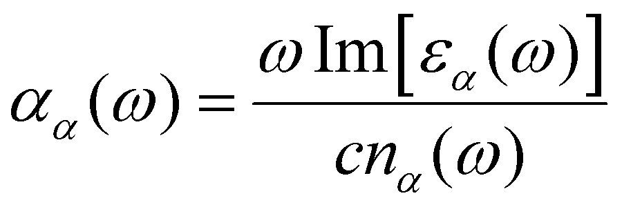
We carried out the atomistic calculations using the Quantum Atomistic ToolKit (QATK)39 package. The DFT approach was implemented in the Kohn–Sham (KS) formulation,40 within the framework of the linear combination of atomic orbitals (LCAO) basis set approach, combined with the pseudopotential (PPs) method and the Perdew–Burke–Ernzerhof (PBE) scheme of the generalized gradient approximation (GGA).41 PseudoDojo42 was used for the LCAO calculation to describe the interaction between ion cores and valence electrons. Valence orbitals were considered with a kinetic energy cut-off of 90 Ry and a 3 × 3 × 1 Monkhorst–Pack k-point mesh was used. We used a vacuum spacing of 16–20 Å perpendicular to the basal planes to avoid image–image interactions across the periodic boundary. The geometries were optimized using a conjugate gradient algorithm where the atoms were allowed to relax until the residual force and energies were smaller than 0.025 eV Å−1 and 1 × 10⁻⁴ eV, respectively. The Brillouin zone was integrated with Blöchl corrections using a broadening width of 0.005 eV.43,44 The van der Waals corrections were included by Grimme's DFT-D3 method,45,46 in order to include the dispersion corrections.Optical calculations were evaluated based on the random phase approximation (RPA).47 The optical properties of the interfaces in this study are discussed by the two components of the dielectric function ε1(ω) and ε2(ω) related to different polarizations in the electric field. The imaginary part ε2(ω) of the dielectric coefficient can be obtained from the direct interband transitions through Fermi's golden rule as in eqn (3)48–50
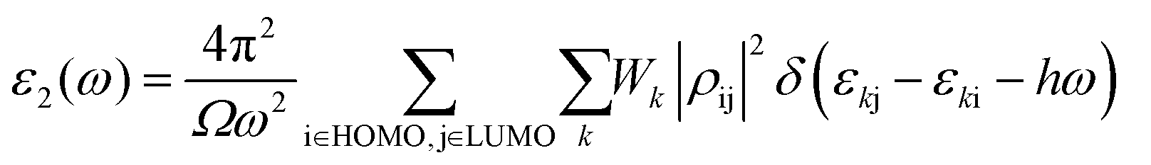 | (3) |
Moreover, the real part (ε1(ω)) of the dielectric constant can be obtained with the following eqn (4)
 | (4) |
 | (5) |
Conclusions
In this work, we used first-principles calculations to predict the adsorption of VO2(M) and VO2(B) structures on different substrates consisting of sapphire(c-cut), sapphire(r-cut), SrTiO3(001), SrTiO3(111), SrNbO3(001), SrNbO3(111), LaAlO3(c-cut), and LaAlO3(r-cut). Using cell optimization and total energy calculations, we compare the relative surface energy, adsorption energy, optical adsorption and dielectric constants of the interfaces. The surface energy calculations show that there is a considerable difference in relaxation of the slabs comparing the VO2(M) and VO2(B) polymorphs. A comparison between surfaces revealed that the surface energies of fully relaxed SrTiO3(111) in VO2(M) and SrNbO3(001) in VO2(B) have considerably larger surface energy than other slabs with 31.8 eV nm−2 and 21.15 eV nm−2, respectively. The adsorption energy calculations revealed that the interface of the VO2(M) polymorph is more favorable on SrTiO3(001) with an adsorption energy of 2.83 eV, while VO2(B) has stability on SrTiO3(111) and sapphire(c-cut) with corresponding adsorption energy values of 0.91 and 1.11 eV, respectively. The optical absorption properties of the most stable (VO2(M)@SrTiO3(001) and VO2(B)@SrTiO3(111)) and less stable (VO2(M)@sapphire(c-cut) and VO2(B)@sapphire (c-cut)) interfaces have been assessed. Both interfaces of VO2(M)@SrTiO3(001) and VO2(B)@SrTiO3(111) showed the adsorption in visible light, while VO2(M)@sapphire(c-cut) and VO2(B)@sapphire(c-cut) indicated the main first adsorption peak in the infrared region of the electromagnetic light. Differences in the stability and optical behaviours of VO2(M) and VO2(B) interfaces on different substrates suggest a path for the creation of new symmetry-mismatched heterostructures applicable in VO2-based electronics and optoelectronic devices.Author contributions
Conceptualization: E. M., E. L. and P. S.; methodology: E. M. and E. L.; validation: E. M., E. L., P. S., L. P., and D. M.; investigation: E. M.; data curation: E. M.; writing – original draft preparation: E. M.; writing – review and editing: E. M., E. L., E. P., P. S., L. P., and D. M.; visualization: E. M.; supervision: P. S.; project administration: E. M., E. L., E. P., P. S., L. P. and D. M. All authors have read and agreed to the published version of the manuscript.Conflicts of interest
There are no conflicts to declare.Acknowledgements
This work is part of the research of H2020 (FETPROACT-EIC-05-2019) “Nanomaterials enabling smart energy harvesting for next-generation Internet-of-Things” (NANO-EH) (grant agreement no. 951761).References
- H. Y. Hwang, Y. Iwasa, M. Kawasaki, B. Keimer, N. Nagaosa and Y. Tokura, Nat. Mater., 2012, 11, 103–113 CrossRef CAS PubMed.
- S. U. M. Khan, M. Al-Shahry and W. B. Ingler Jr, Science, 2002, 297, 2243–2245 CrossRef CAS PubMed.
- J. Jeong, N. Aetukuri, T. Graf, T. D. Schladt, M. G. Samant and S. S. P. Parkin, Science, 2013, 339, 1402–1405 CrossRef CAS PubMed.
- S. Lee, T. L. Meyer, S. Park, T. Egami and H. N. Lee, Appl. Phys. Lett., 2014, 105(22), 223515 CrossRef.
- C. Leroux, G. Nihoul and G. Van Tendeloo, Phys. Rev. B, 1998, 57, 5111 CrossRef CAS.
- C. Wu, X. Zhang, J. Dai, J. Yang, Z. Wu, S. Wei and Y. Xie, J. Mater. Chem., 2011, 21, 4509–4517 RSC.
- R. Basu, M. Sardar and S. Dhara, AIP Conf. Proc., 2018, 1942(1), 030003 CrossRef.
- Y. Oka, S. Sato, T. Yao and N. Yamamoto, J. Solid State Chem., 1998, 141, 594–598 CrossRef CAS.
- N. Ganganagappa and A. Siddaramanna, Mater. Charact., 2012, 68, 58–62 CrossRef CAS.
- C. Wu, F. Feng, J. Feng, J. Dai, J. Yang and Y. Xie, J. Phys. Chem. C, 2011, 115, 791–799 CrossRef CAS.
- Y. Wang, Z. Zhang, Y. Zhu, Z. Li, R. Vajtai, L. Ci and P. M. Ajayan, ACS Nano, 2008, 2, 1492–1496 CrossRef CAS PubMed.
- B.-J. Kim, Y. W. Lee, B.-G. Chae, S. J. Yun, S.-Y. Oh, H.-T. Kim and Y.-S. Lim, Appl. Phys. Lett., 2007, 90(2), 023515 CrossRef.
- L. Huitema, A. Crunteanu, H. Wong and E. Arnaud, Appl. Phys. Lett., 2017, 110(20), 203501 CrossRef.
- Y. Cui, Y. Ke, C. Liu, Z. Chen, N. Wang, L. Zhang, Y. Zhou, S. Wang, Y. Gao and Y. Long, Joule, 2018, 2, 1707–1746 CrossRef CAS.
- N. Ganganagappa and A. Siddaramanna, Mater. Charact., 2012, 68, 58–62 CrossRef CAS.
- E. Mohebbi, E. Pavoni, D. Mencarelli, P. Stipa, E. Laudadio and L. Pierantoni, Front. Mater., 2023, 10, 1145822 CrossRef.
- E. Mohebbi, E. Pavoni, D. Mencarelli, P. Stipa, L. Pierantoni and E. Laudadio, RSC Adv., 2022, 12, 31255–31263 RSC.
- E. Mohebbi, E. Pavoni, D. Mencarelli, P. Stipa, L. Pierantoni and E. Laudadio, Nanoscale Adv., 2022, 4, 3634–3646 RSC.
- J. Heyd and G. E. Scuseria, J. Chem. Phys., 2004, 121, 1187–1192 CrossRef CAS PubMed.
- H. W. Verleur, A. S. Barker Jr and C. N. Berglund, Phys. Rev., 1968, 172, 788 CrossRef CAS.
- J. Lourembam, A. Srivastava, C. La-o-Vorakiat, L. Cheng, T. Venkatesan and E. E. M. Chia, Sci. Rep., 2016, 6, 25538 CrossRef CAS PubMed.
- A. Ruzsinszky, G. I. Csonka, O. A. Vydrov, G. E. Scuseria, L. A. Constantin, X. Zhou and K. Burke, Phys. Rev. Lett., 2008, 100, 136406 CrossRef PubMed.
- A. Chen, Z. Bi, W. Zhang, J. Jian, Q. Jia and H. Wang, Appl. Phys. Lett., 2014, 104(7), 071909 CrossRef.
- A. Srivastava, H. Rotella, S. Saha, B. Pal, G. Kalon, S. Mathew, M. Motapothula, M. Dykas, P. Yang and E. Okunishi, APL Mater., 2015, 3(2), 026101 CrossRef.
- J. Jian, A. Chen, Y. Chen, X. Zhang and H. Wang, Appl. Phys. Lett., 2017, 111(15), 153102 CrossRef.
- F. Shayeganfar and A. Rochefort, Langmuir, 2014, 30(32), 9707–9716 CrossRef CAS PubMed.
- S. Woo, H. Jeong, S. A. Lee, H. Seo, M. Lacotte, A. David, H. Y. Kim, W. Prellier, Y. Kim and W. S. Choi, Sci. Rep., 2015, 5, 8822 CrossRef PubMed.
- T. Stirner, J. Sun and M. Aust, Phys. Procedia, 2012, 32, 635–639 CrossRef CAS.
- K. Krishnaswamy, C. E. Dreyer, A. Janotti and C. G. Van de Walle, Phys. Rev. B, 2014, 90, 235436 CrossRef.
- R. Jayan and M. M. Islam, ACS Appl. Mater. Interfaces, 2021, 13, 35848–35855 CrossRef CAS PubMed.
- E. Mohebbi, E. Pavoni, L. Pierantoni, P. Stipa, G. M. Zampa, E. Laudadio and D. Mencarelli, Results Phys., 2024, 107415 CrossRef.
- A. Maniyar and S. Choudhary, RSC Adv., 2020, 10, 31730–31739 RSC.
- L. Liu, N. He, T. Wu, P. Hu and G. Tong, Chem. Eng. J., 2019, 355, 103–108 CrossRef CAS.
- J. Hou, B. Wang, Z. Ding, R. Dai, Z. Wang, Z. Zhang and J. Zhang, Appl. Phys. Lett., 2017, 111, 072107 CrossRef.
- B. Guo, D. Wan, A. Ishaq, H. Luo and Y. Gao, J. Alloys Compd., 2017, 715, 129–136 CrossRef CAS.
- S. Saha, T. P. Sinha and A. Mookerjee, J. Phys.: Condens. Matter, 2000, 12, 3325 CrossRef CAS.
- A. K. Harman, S. Ninomiya and S. Adachi, J. Appl. Phys., 1994, 76, 8032–8036 CrossRef CAS.
- M. Schubert, T. E. Tiwald and C. M. Herzinger, Phys. Rev. B, 2000, 61, 8187 CrossRef CAS.
- S. Smidstrup, T. Markussen, P. Vancraeyveld, J. Wellendorff, J. Schneider, T. Gunst, B. Verstichel, D. Stradi, P. A. Khomyakov and U. G. Vej-Hansen, J. Phys.: Condens. Matter, 2019, 32, 015901 CrossRef PubMed.
- H. S. Yu, S. L. Li and D. G. Truhlar, J. Chem. Phys., 2016, 145(13), 130901 CrossRef PubMed.
- F. Favot, A. Dal Corso and A. Baldereschi, J. Chem. Phys., 2001, 114, 483–488 CrossRef CAS.
- M. J. van Setten, M. Giantomassi, E. Bousquet, M. J. Verstraete, D. R. Hamann, X. Gonze and G.-M. Rignanese, Comput. Phys. Commun., 2018, 226, 39–54 CrossRef CAS.
- E. Laudadio, E. Mohebbi, E. Pavoni, C. Minnelli, S. Sabbatini and P. Stipa, Colloids Surf., A, 2023, 667, 131388 CrossRef CAS.
- E. Pavoni, E. Mohebbi, P. Stipa, L. Pierantoni, D. Mencarelli, M. Dragoman, M. Aldrigo and E. Laudadio, Nanoscale Adv., 2023, 5, 2748–2755 RSC.
- L. Goerigk, Non-Covalent Interact. Quantum Chem. Phys., 2017, 195–219 CrossRef CAS.
- F. Sedona, M. M. S. Fakhrabadi, S. Carlotto, E. Mohebbi, F. De Boni, S. Casalini, M. Casarin and M. Sambi, Phys. Chem. Chem. Phys., 2020, 22, 12180–12186 RSC.
- G. P. Chen, V. K. Voora, M. M. Agee, S. G. Balasubramani and F. Furche, Annu. Rev. Phys. Chem., 2017, 68, 421–445 CrossRef CAS PubMed.
- K. Kolwas and A. Derkachova, Nanomaterials, 2020, 10, 1411 CrossRef CAS PubMed.
- T. Micklitz, A. Morningstar, A. Altland and D. A. Huse, Phys. Rev. Lett., 2022, 129, 140402 CrossRef CAS PubMed.
- E. Mohebbi and M. M. S. Fakhrabadi, J. Mater. Sci. Eng. B, 2022, 281, 115745 CrossRef CAS.
| This journal is © The Royal Society of Chemistry 2024 |