
 Open Access Article
 This Open Access Article is licensed under a
 Creative Commons Attribution 3.0 Unported Licence
Copper-based core–shell metamaterials with ultra-broadband and reversible ENZ tunability†
Anastasiia
Zaleska
 *,
Alexey V.
Krasavin
,
Anatoly V.
Zayats
and
Wayne
Dickson
*,
Alexey V.
Krasavin
,
Anatoly V.
Zayats
and
Wayne
Dickson
Department of Physics and London Centre for Nanotechnology, King's College London, Strand, London WC2R 2LS, UK. E-mail: anastasiia.zaleska@kcl.ac.uk
First published on 21st May 2024
Abstract
The inexpensive fabrication of large-area plasmonic nanostructures is essential for the timely technological exploitation of plasmonic phenomena in diverse fields, from photocatalysis to sensitive biological and chemical sensing. Self-assembled porous alumina templates offer such an inexpensive and scalable route to the fabrication of metamaterials, with the ability to cover macroscale areas while retaining nanometric control over the constituent dimensions. Traditionally employing gold and silver, metamaterials have often overlooked less expensive but highly functional transition metal alternatives. Copper presents an interesting metamaterial constituent due to its cost, abundance, intrinsic optical properties and established use as a catalyst, with applications for both metallic copper and its main oxidation states (Cu2O and CuO). In this work, we have fabricated plasmonic metamaterials comprised of an array of copper nanorods with controllable dimensions with optical properties determined by the geometry of the nanorod array and the formation of copper oxide shells on the nanorods. The high refractive index sensitivity of these metamaterials enabled the complex electrochemistry of copper to be monitored via in situ visible light spectroscopy during cyclic voltammetry in a sodium hydroxide solution and the subsequent correlation of the optical spectra with the oxidation and reduction processes. Anodising the metamaterial at a fixed potential enables the controllable and reversible growth of a nanometric shell of copper oxide, at growth rates of approximately 0.23 nm min−1, confirmed by in situ optical spectroscopy and electromagnetic simulations. This not only introduces an additional mechanism for broad spectral tuning of the epsilon-near-zero spectral range and the corresponding extinction peak by >100 nm, but also provides a scalable method to fabricate designer core–shell metamaterials with new functionalities.
1 Introduction
The recent drive to exploit plasmonic hot-carrier effects in sensing and photocatalysis has caused an upsurge in the development of new material approaches in plasmonics and a drift away from the traditional plasmonic noble metals.1–5 In the past few years, this has led to a wide search for alternative plasmonic media that are either inexpensive or provide additional functionalities. Copper, as one such alternative plasmonic constituent, benefits from both high natural abundance and low cost, making it an intrinsically attractive material for commercial exploitation. In particular, copper electrodes have been used as efficient electrocatalysts for reactions such as CO2 reduction,6–11 water splitting,12–15 self-cleaning9,16 and plasmon-induced organic transformations.17,18In this paper, for the first time, we introduce a new plasmonic metamaterial based on an array of copper nanorods with ultrabroad and reversible ENZ tunability, engineered by taking advantage of nanoscale electrochemical oxidation and reduction of the nanorod surface over the macroscale array (≈1 cm2 and ≈1011 nanorods). Herein, we describe the fabrication method as well as the structural and optical characterisation of highly uniform large-area copper-based plasmonic metamaterials. These metamaterials are fabricated using anodic aluminium oxide (AAO) as a template.19,20 This technique has considerable advantages in terms of scalability, whilst also providing both nanometric control of the constituents and high uniformity, resulting in broad spectral tunability of the resonant modes and plasmonic functionality.21–23
Beyond the well-known application of copper as an efficient catalyst, copper (as well as silver) nanomaterials are often at a disadvantage for more traditional plasmonic applications compared to those produced using noble metals due to the potential for oxidation. In more recent work, oxidation has been addressed by coating the Cu nanomaterials with various passivation layers deposited by atomic layer deposition (ALD).24 However, the oxides of copper are also well-established photo- and electrocatalysts,25–29 and the results of our work have resulted in the development of bespoke core–shell Cu/CuxO light harvesting metamaterials with nanometrically controllable dimensions and designer optical properties. Here, we describe the procedure for the controllable growth and reduction of copper oxide layers of nanometric thickness via electrochemical oxidation in an alkaline electrolyte. This process was monitored in real-time using in situ visible light spectroscopy and the results were validated using numerical modelling. Furthermore, optical spectra were obtained in real-time during cyclic voltammetry and correlated with the electrochemical processes. This methodology presents the opportunity to combine the catalytic functionality of copper and its oxides with plasmonic light harvesting and catalytic enhancement in high surface area metamaterials.
2 Results and discussion
2.1 Fabrication and optical characterisation of copper nanorod metamaterials
The fabrication process begins by magnetron sputtering 10 nm of tantalum pentoxide (Ta2O5) onto a 0.7 mm thick glass (SiO2) substrate to act as an adhesion layer. This is followed by the sputter deposition of 8 nm of gold (Au) and finally 280 nm of aluminium (Al) (Fig. 1a). The aluminium is then electrochemically anodised at 1 °C in a sulphuric acid (H2SO4) solution at an applied constant voltage of 25 V, which results in formation of a porous AAO matrix. The barrier layer formed at the bottom of the pores was removed by etching in a 30 mM sodium hydroxide (NaOH) solution, which provides access to the underlying gold layer serving as an electrode for subsequent electrodeposition. In addition to the removal of the barrier layer, the duration of this etching step determines the final diameter of the pores and provides geometrical control that translates into spectral tunability of the optical properties of the final metamaterial.20 For further fabrication details see the Methods section.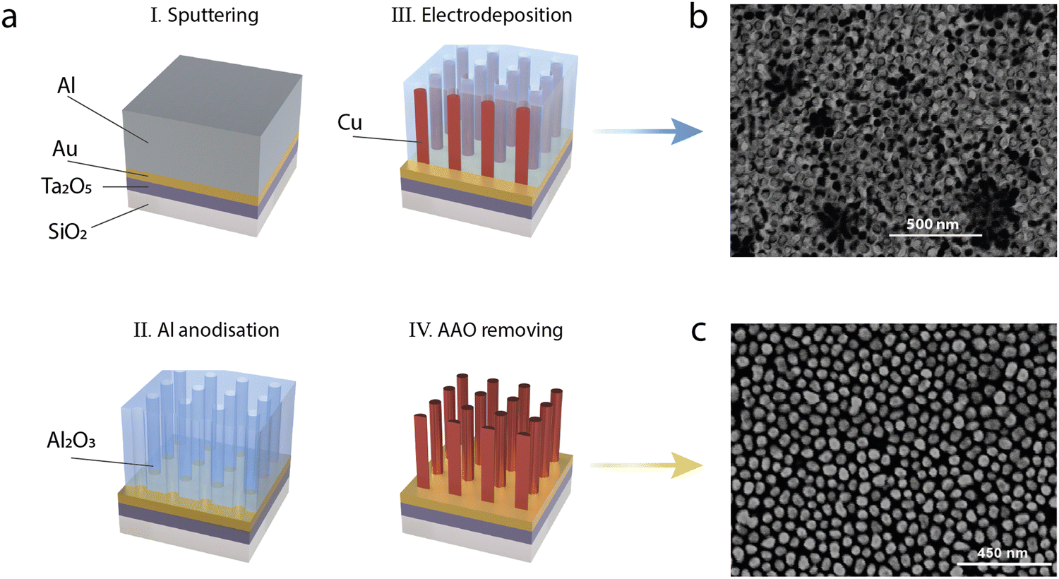 | ||
| Fig. 1 (a) A schematic diagram of the fabrication steps to form arrays of copper nanorods using AAO templates. (I) The formation of thin multilayer films by magnetron sputtering, (II) the anodisation of aluminium to create a porous AAO template and consequential removal of the barrier layer, (III) the electrodeposition of copper into the alumina pores, (IV) the Cu nanorods exposed to air after the removal of the AAO. Top-view SEM images of the resulting array of copper nanorods (b) before and (c) after complete removal of the alumina using 0.3 M NaOH. | ||
In order to form the final plasmonic metamaterial, copper was electrodeposited into the pores of the alumina template from a 0.12 M copper sulfate (CuSO4) solution mixed with 0.49 M H3BO3 under a constant voltage of −2.8 V. Electrodeposition was carried out at room temperature in a custom-made electrochemical cell consisting of a three-electrode configuration, with platinum (Pt) foil as a counter electrode and a silver–silver chloride (Ag/AgCl) reference electrode. Fig. 1b and c show SEM images of a uniform array of vertically-aligned copper nanorods before and after the removal of the alumina template via chemical etching in 0.3 M NaOH. The length of the metallic nanorods comprising the metamaterial is determined by the electrodeposition duration and can be varied from 30 nm to the limiting value dictated by the thickness of the porous AAO (typically 275–400 nm). Energy-dispersive X-ray spectroscopy analysis (EDX), confirmed an abundance of copper and the elemental composition in the metamaterial architecture.
The optical properties of the fabricated metamaterials are determined by polarisation-resolved visible light spectroscopy. Experiments were performed in transmission using both TM- and TE-polarised light at various angles of incidence. Fig. 2 shows the experimental extinction spectra of copper nanorods embedded in the alumina matrix as a function of the angle of incidence for both polarisations. The optical properties revealed are those typical for such anisotropic uniaxial metamaterials, exhibiting two extinction peaks.30 Under normal incidence illumination, the short-wavelength peak, present at a wavelength of approximately 570 nm, is related to the excitation of a transverse dipolar plasmonic resonance of the nanorod metal core (T-mode). Increasing the angle of incidence and using TM polarised light reveals a second extinction peak at 620 nm, associated with the high attenuation of the TM mode inside the metamaterial in the epsilon-near-zero (ENZ) regime when the effective component of the permittivity perpendicular to the substrate (parallel to the long axis of the nanorods) is close to zero (see Methods for the description of metamaterial effective optical properties). The spectral width of the ENZ peak (and hence damping) does not differ significantly with respect to that observed for gold nanorod-based metamaterials with a similar nanoscale geometry.30 The position of the ENZ extinction peak (in particular) may be tuned throughout the visible spectrum by varying the dimensions of the individual rods (Fig. S1, ESI†). At the same time, the spectral position of the ENZ peak, together with that of thickness-dependent resonances appearing in the metamaterial slab is determined by the electromagnetic coupling between the nanorods affected by the surrounding refractive index, making such metamaterials particularly suitable for sensing applications (Fig. S2, ESI†).22,31,32
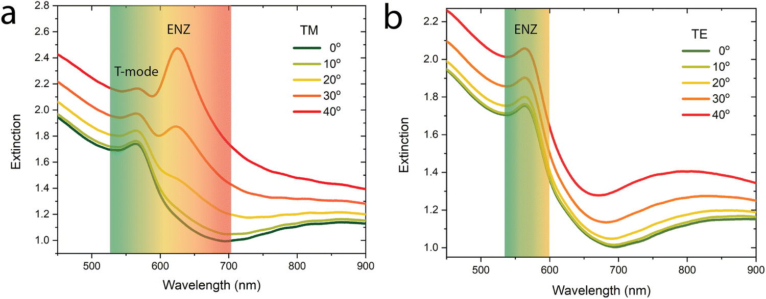 | ||
| Fig. 2 Measured extinction spectra of Cu nanorod arrays embedded in an alumina matrix under (a) TM- and (b) TE-polarised light illumination at various angles of incidence. The metamaterials are comprised of nanorods with 17 nm radius, 220 nm length, and a mean centre-to-centre separation of 85 nm. | ||
2.2 The electrochemistry of Cu metamaterials
Prior to all electrochemical studies, the alumina matrix surrounding the nanorods was removed using a NaOH solution (0.3 M NaOH for approximately 5 minutes) revealing arrays of free-standing nanorods, conductively connected via the remaining gold underlayer. A custom-made three-electrode electrochemical cell was used, comprising a platinum counter electrode, a saturated Ag/AgCl reference electrode and a 0.15 M NaOH electrolyte with the copper nanorod metamaterial serving as the working electrode. The optical properties of the metamaterials were continuously monitored using in situ transmission spectroscopy (200 ms per spectrum) with TM polarised light at an incident angle of 40°, allowing both extinction peaks to be observed. First, cyclic voltammetry (CV) was performed for five cycles in the potential range of Cu2O and CuO formation at a sweep rate of 0.01 V s−1 in order to confirm the presence and position of the oxidation and reduction peaks and the stability of the nanostructures over cycling (Fig. S3, ESI†). The material was initially precycled to obtain a stable CV scan.
Fig. 3a shows the corresponding cyclic voltammogram after one cycle, verifying the potential for the formation of Cu2O at −0.38 V (designated A1) and a broad anodic peak at a maximum of +0.06 V (designated A2) corresponding to further Cu(I) to Cu(II) oxidation. Both the oxidation and reduction peaks can be clearly identified as expected from the literature33–35 and the results obtained for a previously anodised copper thin film (Fig. S4, ESI†).
 | ||
| Fig. 3 The study of the optical response of a copper nanorod electrode in a 0.15 M NaOH within a (a) CV sweep at a scan rate of 0.01 V s−1. Colour points are positioned on the reduction/oxidation peaks (b)–(e). Each set of extinction spectra transition from one coloured point on the CV chart to another, with the beginning and end points are designated by bold lines of the same colour. Each spectrum is labelled with its respective concluding reaction. The parameters of the copper nanorod metamaterial are 180 nm length, 23 nm radius and 80 nm period. | ||
The optical properties of the metamaterial during the CV sweep are summarised in Fig. 3b–e. The colours overlayed on the cyclic voltammogram (yellow, green, blue and pink) correspond to the four oxidation/reduction reactions occurring at the surface of the copper nanorods. The experimental extinction spectra measured during one cycle of the CV sweep are thus divided into four plots (Fig. 3(b)–(e)) to illustrate how the optical properties of the sample evolve through each stage of the process. The border of each set of extinction spectra is coloured to match the highlighted regions in the CV sweep. Additionally, the colour of the curves in each plot corresponds to the coloured circular markers at specific points in that section of the CV sweep, showing the direction of transition of the optical properties (also indicated by arrows). These markers are located at the starting potential (0 V) and each key oxidation/reduction peak.
The extinction spectrum of the metamaterial is initially characterised by a single peak (Fig. 3b, red curve), as the transverse resonance and ENZ extinction regions overlap in wavelength, which is typical for this architecture of nanorod metamaterial with these dimensions (a 23 nm diameter, an 80 nm spacing) in an aqueous solution (n ∼ 1.33). In addition, the broad width of the extinction peak is the result of a mixed oxide/hydroxide surface following previous CV sweeps.
Our analysis of the in situ spectroscopy begins at a potential of 0 V vs. Ag/AgCl at the beginning of the reductive cathodic sweep. As the potential decreases towards cathodic peak C2 (Fig. 3a) located at a potential of −0.31 V vs. Ag/AgCl, a non-monotonous change in the extinction maximum is observed (Fig. 3b). At low negative potentials, this is characterised by both a blue-shift of the extinction peak and a decrease in its magnitude. This may be explained by the decomposition of dissolved Cu(OH)42− to CuO,36 increasing the losses due to the large imaginary component of the dielectric constant of CuO (Fig. S5, ESI†). However, as the potential reaches C2, this behaviour is reversed, and Fig. 3b shows a red-shift of the peak and an increase in its magnitude. This region of the sweep and peak C2 in particular is assigned to the partial reduction of CuO to Cu2O,37 while the red-shift of the extinction peak and increase in its magnitude are characteristics of the change in the dielectric permittivity of Cu2O having a larger real and a lower imaginary components in this spectral range, compared to CuO (Fig. S5, ESI†). At more negative potentials towards peak C1 a series of concurrent reduction processes, consisting of the reduction of Cu2+ species and Cu2O to metallic Cu, take place. This is readily observed in the extinction spectra shown in Fig. 3c, where there is a dramatic increase of the magnitude of the extinction peak together with a blue-shift in its spectral position. The increase in extinction is a result of the reduction of any remaining (lossy) CuO/Cu2O and an increase in the metallic content of the nanorods. In this scenario, the transverse resonance would experience a blue-shift due to the lower effective dielectric constant surrounding the metal core. For the ENZ extinction peak, the blue-shift is a result of the increase in the metal filling factor (f in eqn (3)) with a commensurate decrease in the dielectric constant surrounding the nanorods. From the perspective of the nanorods in the array, each nanorod experiences a decrease in the surrounding dielectric constant, their aspect ratio decreases and the dipolar coupling increases between adjacent rods – all contributing to the observed blue-shift.
As the anodic sweep begins, the nanorods are comprised entirely of metallic copper. As the potential is increased from −1.2 V vs. Ag/AgCl, the surface first becomes hydroxylated, with the formation of Cu(OH)2, before reaching anodic peak A1 located at a potential of −0.35 V vs. Ag/AgCl where the formation of Cu2O takes place (Fig. 3d).38 Examination of Fig. 3d shows that as the potential increases and the formation of Cu2O begins, creating Cu/Cu2O core–shell nanorods, there is a distinct red-shift and broadening of the main extinction peaks. The explanation is precisely the reverse of that described for peak C1 above: an increase in the effective dielectric constant surrounding the nanorods via the growth of Cu2O and a decrease in the diameter of the metallic nanorods (and hence the metal filling fraction inside the nanorod η). Despite the red-shift primarily affecting the ENZ extinction peak as we shall see later in the manuscript, two distinct peaks are not observed, mainly due to the small magnitude of the red-shift (∼30 nm) and the optical loss intrinsic to Cu2O at this wavelength compared with the aqueous electrolyte. Further increasing the potential towards peak A2 results in a dramatic transformation of the extinction spectrum (Fig. 3e), as first the formation of Cu(OH)42− and Cu(OH)2 takes place (up-slope) followed by potential oxidation to CuO.
The reduction in the overall extinction and dramatic broadening of the peak may be explained once again by comparing the relative permittivity of Cu2O and CuO, the latter characterised by a significantly lower real part of epsilon and an order of magnitude higher imaginary component at a wavelength of 600 nm (Fig. S5, ESI†). Despite the paucity of data on the refractive index of copper hydroxides, the general behaviour of the extinction spectra is qualitatively reproduced by numerical modelling of a Cu/CuO core–shell system with various CuO shell thicknesses (Fig. S6, ESI†). The situation is further complicated as the voltage increases following peak A2, as the slow hydroxylation of CuO to soluble Cu(OH)42− is expected to occur.36 However, recent work by Topali et al.39 claims there is little evidence of CuO formed in situ, and instead of the often stated CuO/Cu(OH2) duplex layer formed following anodic peak A240 a complex mixed oxide/hydroxide layer containing metastable Cu4O3 is formed, with the latter becoming CuO following removal from the electrolyte. The precise composition of the film cannot be determined from the measurements here, as the dielectric permittivity of Cu4O3 at a wavelength around 600 nm while significantly different to that of CuO, also has a larger imaginary component than Cu2O (Fig. S7, ESI†), which could result in a similar spectral shape, depending on the exact layer thicknesses and hierarchical distribution of the different oxides. Further detailed analysis of the composition in this complex region is beyond the aim and scope of this work.
2.3 Oxidation and reduction
 | ||
| Fig. 4 (a) The measured extinction spectra during the surface oxidation of the copper nanorod material in a 0.15 M NaOH electrolyte solution at −0.39 V vs. Ag/AgCl. (b) The calculated extinction spectra as a function of the shell thickness of Cu2O with the increase of the aspect ratio. All extinction spectra were acquired at an incident angle of 40° using TM polarised light. The initial parameters of the copper nanorods: a 13.2 nm radius, a 188.6 nm length, and an 80 nm period. | ||
To confirm the observations in Fig. 4a, further aid understanding the optical behaviour of the core–shell Cu/Cu2O metamaterials, and gain an insight into the thicknesses of the created oxide layers, the extinction spectra were calculated as a function of the Cu2O shell thickness using full-vectorial simulations of a square nanorod array (for details see Methods). Fig. 4b shows the resulting extinction calculated as a function of the Cu2O shell thickness on a copper nanorod surface under plane-wave illumination with TM-polarised light at 40° incidence. The dimensions used in the simulations matched the fabricated nanomaterials, with the initial and final geometrical parameters (diameter, length) obtained from SEM and AFM images. The anodisation process was simulated to include the consumption of the metallic Cu and formation of Cu2O as well as the volume expansion caused by the oxidation. The volume expansion was estimated to be approximately 30% which is in agreement with previous measurements performed on a freshly formed Cu(I) oxide layer of a similar thickness on a copper film. As observed experimentally, the calculations in Fig. 4b show the ENZ extinction peak undergoing a red-shift as the thickness of the Cu2O is increased. Due to the lack of material inhomogeneity in the simulation, the linewidth of the peaks is appreciably narrower, despite the simulations using a mean-free restricted path model for the permittivity of Cu. Comparing these results with the experimental spectra shown in Fig. 4a, both the red-shift of the ENZ peak and the reduction of its magnitude are reproduced. Moreover, this analysis allows us to estimate the growth rate of the oxide shell during the anodisation to be 0.23 nm min−1, matching the experimentally measured spectral position of the ENZ peak changing approximately linearly with the anodisation time to the simulated one changing linearly with the oxide Cu2O thickness (Fig. S8, ESI†). The oxide shell thickness is estimated to exceed 7 nm, dramatically shifting the ENZ extinction peak into the near-IR range. For clarification of the mechanisms underpinning the dramatic wavelength shift, calculations were also performed varying the oxide shell thickness, but maintaining a constant copper nanorod diameter i.e. ignoring the reduction in radius due to oxidation. The results are shown in Fig. S9 (ESI†) and, as expected, demonstrate a significantly reduced tunability, highlighting the combination of optical processes contributing to the rapid red-shift observed in the experiment. Additionally, after detaching the core–shell Cu/Cu2O nanostructures from a glass substrate, the formation of copper oxide shell around the copper nanorod-based metamaterial was revealed using transmission electron microscopy (TEM) and energy dispersive spectroscopy (EDS) mapping, as shown in Fig. S10 (ESI†). This also allowed us to estimate the shell thickness of the formed oxide layer, which was found to be in agreement with the calculated prediction based on the optical response of the metamaterial. The oxidation state of Cu in the fabricated core–shell Cu/Cu2O nanostructures was analysed by X-ray photoelectron spectroscopy (XPS) confirming their composition (Fig. S11, ESI†).
The extinction spectra of a Cu/CuO core–shell nanorod metamaterial were calculated for comparison and to fully explore the optical properties of these core–shell geometries (Fig. S6, ESI†). Compared to copper oxide, the dielectric permittivity of copper(II) oxide is characterised by a significantly larger imaginary component and a smaller real component at wavelengths above 525 nm. The large imaginary component is responsible for additional broadening of the ENZ extinction peak as the thickness of the copper(II) oxide shell is increased, and indeed it is not discernible in the calculated spectra until the shell reaches 5 nm in thickness at which point the ENZ peak is red-shifted to a wavelength greater than approximately 800 nm where the imaginary component of the permittivity of CuO begins to decrease significantly (Fig. S5, ESI†).
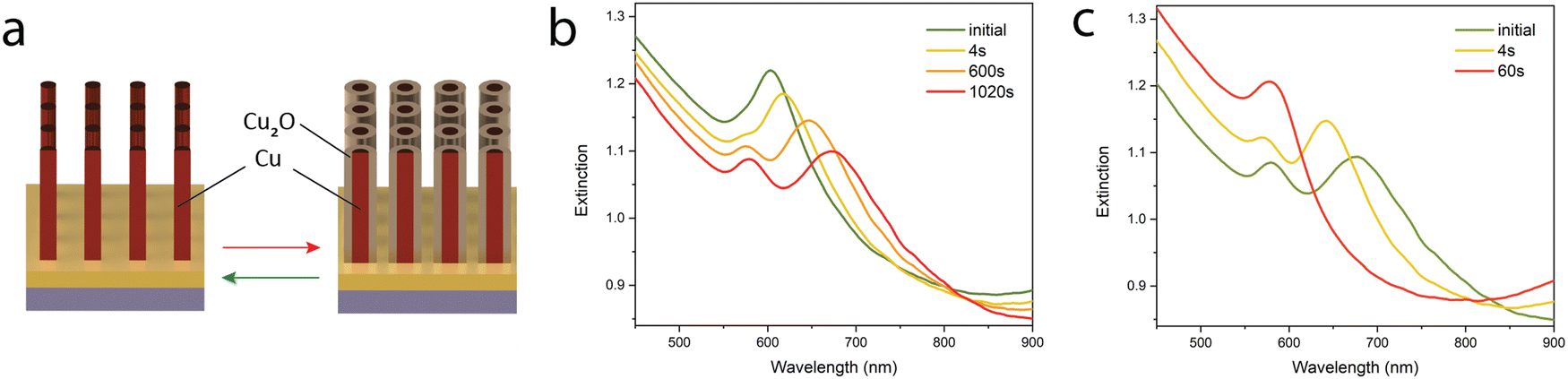 | ||
| Fig. 5 (a) The schematics of electrochemical formation of copper oxide on the Cu nanorod surface. The measured extinction spectra during (b) the oxidation and (c) the reduction of the copper electrode for 20 minutes in an electrochemical cell with a 0.15 M NaOH solution. | ||
3 Conclusions
In this work, we have presented an inexpensive fabrication process for plasmonic metamaterials based on subwavelength arrays of copper nanorods. The method described has considerable advantages in terms of scalability whilst retaining nanometric control of the constituent nanorods which provides broad plasmonic tunability throughout the visible spectrum. The complex electrochemistry of copper in alkaline electrolytes has been studied using the cyclic voltammetry combined with in situ optical spectroscopy to interrogate the optical properties of the metamaterial. The extraordinary refractive index sensitivity displayed by metamaterials of this architecture provides a unique method to monitor the surface composition in real-time, which together with other techniques, can help to provide new insights into the complex electrochemical processes. The anodisation of copper in alkaline solutions offers a route to the scalable synthesis of core–shell Cu–CuxO nanorod metamaterials. The anodisation of the copper is highly controllable and reversible, with the oxidation rate estimated to be approximately 0.23 nm min−1, enabling the fabrication of ultrathin shells of copper oxides with sub-nanometer precision. Using this process, a reversible spectral shift of >100 nm has been demonstrated for the ENZ extinction peak. This spectral shift is only constrained by the initial dimensions of the nanorods comprising the metamaterial. The implemented fabrication process provides a novel route to both tune the optical properties of the metamaterial and more importantly, create functional oxide surfaces of controllable thickness for the development of highly efficient plasmonic photocatalysts and sensitive sensors.Specifically, with regard to the photo and photo-electrocatalytic reduction of CO2, the copper-based metamaterials developed here have the properties to be considered excellent candidates as they provide the high surface area, excellent light absorption, refractive index-based monitoring of the catalytic surface, the potential for SERS monitoring of adsorbed surface species41 while the ability to electrically address the copper constituents also enables electrocatalytic surface modification and restructuring for enhanced efficiency and designer specificity.42 We expect that Cu/Cu2O core–shell nanomaterials may be more durable, with their stability depending on the thickness of the anodised oxide layer.
4 Methods
4.1 Fabrication details
Magnetron sputtering (The Kurt J. Lesker Company PVD75 Sputter System) was used as the deposition method for the production of the multilayer thin films on transparent glass substrates (Corning Eagle XG, uncoated) composed of tantalum pentoxide (Ta2O5, 99.95% purity), gold (Au, 99.99%) and aluminium (Al, 99.99%). Previous ellipsometry measurements confirmed the presence of stoichiometric Ta2O5, which had been detected by low absorption in the visible spectrum.43 The anodisation process was performed at 2 °C in a specifically designed electrochemical cell filled with a 0.3 M H2SO4 electrolyte solution. A constant voltage of 25 V was applied between the sample (anode) and the Pt foil as a counter electrode (cathode). The anodised samples were subsequently etched in 30 mM NaOH to achieve pore widening and to remove the barrier layer. Copper electrodeposition was performed with a three-electrode system at an applied voltage of −2.8 V using a 0.12 M copper sulphate (CuSO4) solution mixed with 0.49 M H3BO3. The length of the nanorods was controlled with the electrodeposition time. The sample was etched in 30 mM NaOH to remove the AAO matrix and expose the metamaterial to air.4.2 Characterisation techniques
All scanning electron microscopy images were taken with a Zeiss EVO LS15 Scanning Electron Microscope with Oxford Instruments Energy-Dispersive X-Ray Spectroscopy systems. The images were processed with ImageJ. TEM images were obtained with a JEOL JEM F200 transmission electron microscope.Optical spectroscopy was performed in a custom-built system using plane-polarised, collimated white light from a tungsten-halogen lamp. After passing through the sample, the light was collected by an objective lens and coupled to a spectrometer (Ocean Optics QE Pro) via a multimode optical fibre. To investigate the linear optical properties of nanostructures, transmission spectra in various surrounding media were acquired as functions of the angle and polarisation of the incident light. The electrochemical oxidation process was continuously monitored in real-time in transmission using in situ visible light spectroscopy spectroscopy (200 ms per spectrum) with TM polarised light at an incident angle of 40°.
4.3 Effective medium theory of a nanorod-based metamaterial
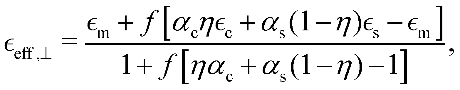
As the nanorod diameter is much smaller than the wavelength, the effective optical properties of square or randomly distributed 2D arrays of oriented nanorods are calculated using effective medium theories in the long-wavelength (quasi-static) limit within the Maxwell Garnett approximation.44,45 Each nanorod is considered to be in a field produced by the illuminating wave and the averaged field generated by all other nanorods. The effective dielectric permittivity of a metamaterials in this case is calculated by averaging the overall electric and electric displacement fields. | (1) |
Due to its symmetry, the nanorod array behaves as a highly anisotropic uniaxial medium with the permittivity in the major axes given by a diagonal tensor  with effective permittivity components perpendicular (⊥) and parallel (‖) to the optical axis directed along the nanorods. Using eqn (1) and carefully averaging E and D along the major axes one obtains the following expressions for the permittivity components:45
 | (2) |
and
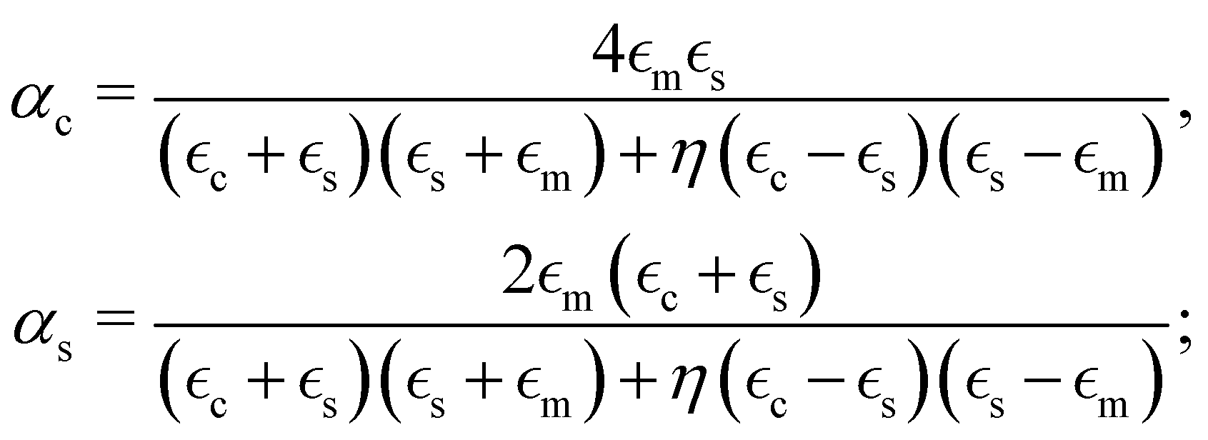
 | (3) |
 and
and  are the permittivities of the core, shell and the dielectric matrix, respectively, f is the nanorod filling factor inside the unit cell (in the case of a square nanorod arrangement equal to π(rc + ts)2/a2) and η = rc2/(rc + ts)2 is the core filling factor inside the nanorod, with rc being the radius of the core, ts the thickness of the shell and a the array spacing. With an absence of artificial magnetic response in the nanorods and zero material magnetism at optical frequencies μeff = 1.
4.4 Modelling of the optical response of Cu-based metamaterials
Numerical modelling was performed using 3D finite-element-method simulations in a frequency domain using the commercial software package (CST Microwave Studio). The plasmonic system was represented as an idealised square array. Taking advantage of the symmetry of the structure, a unit cell of the array was modelled, with periodic boundary conditions having the proper phase shift defined by the incident angle set on its side boundaries. The incident plane electromagnetic wave was generated using a top port boundary condition, which also ensures the absence of back-reflection from this face. A similar port, but without plane-wave excitation was set at the bottom. The optical constants (n and k) for copper oxides, CuO and Cu2O, were taken from ref. 46 (Fig. S5, ESI†), the refractive index of the surrounding electrolyte solution is practically equal to that of water and was taken to be 1.33. The optical properties of copper presented in Fig. S13 (ESI†) were taken from tabulated experimental data47 and corrected by setting the electron mean free path to 3.3 nm,30,48 which takes into account the highly polycrystalline nature of copper due to the employed electrodeposition fabrication process. The optical properties of Au, Al2O3, Ta2O5 and SiO2 were taken from ref. 47 and 49–51 respectively.Conflicts of interest
There are no conflicts to declare.Acknowledgements
This work was supported by the UK EPSRC projects EP/M013812/1 and EP/W017075/1. The authors gratefully acknowledge Dr Diptiranjan Paital, Dr William Wardley and Mr William Luckhurst in the Department of Physics and the Centre for Ultrastructural Imaging (CUI) of King’s College London for their support and expertise in this work.References
- P. Wang, A. V. Krasavin, L. Liu, Y. Jiang, Z. Li, X. Guo, L. Tong and A. V. Zayats, Molecular Plasmonics with Metamaterials, Chem. Rev., 2022, 122, 15031–15081 CrossRef CAS PubMed.
- M. W. Knight, N. S. King, L. Liu, H. O. Everitt, P. Nordlander and N. J. Halas, Aluminum for Plasmonics, ACS Nano, 2014, 8, 834–840 CrossRef CAS PubMed.
- W. P. Wardley, F. J. Rodrguez-Fortuno, A. V. Zayats and W. Dickson, Improving propagation lengths of ultraviolet surface plasmon polaritons on thin aluminium lms by ion milling, J. Phys. D: Appl. Phys., 2019, 52, 074004 CrossRef.
- R. Bower, C. P. T. McPolin, A. V. Krasavin, A. V. Zayats and P. K. Petrov, Temperature stability of individual plasmonic Au and TiN nanodiscs, Opt. Mater. Express, 2022, 12, 3471 CrossRef CAS.
- A. Y. Bykov, A. Shukla, M. van Schilfgaarde, M. A. Green and A. V. Zayats, Ultrafast Carrier and Lattice Dynamics in Plasmonic Nanocrystalline Copper Sulfide Films, Laser Photonics Rev., 2021, 15, 2000346 CrossRef CAS PubMed.
- D. Kim, C. S. Kley, Y. Li and P. Yang, Copper nanoparticle ensembles for selective electroreduction of CO2 to C2–C3 products, Proc. Natl. Acad. Sci. U. S. A., 2017, 114, 10560–10565 CrossRef CAS PubMed.
- X. Zhang, F. Han, B. Shi, S. Farsinezhad, G. P. Dechaine and K. Shankar, Photocatalytic Conversion of Diluted CO2 into Light Hydrocarbons Using Periodically Modulated Multiwalled Nanotube Arrays, Angew. Chem., Int. Ed., 2012, 51, 12732–12735 CrossRef CAS PubMed.
- S. C. Roy, O. K. Varghese, M. Paulose and C. A. Grimes, Toward Solar Fuels: Photocatalytic Conversion of Carbon Dioxide to Hydrocarbons, ACS Nano, 2010, 4, 1259–1278 CrossRef CAS PubMed.
- Q. Zhu, Y. Zhang, J. Wang, F. Zhou and P. K. Chu, Microwave Synthesis of Cuprous Oxide Micro-/Nanocrystals with Different Morphologies and Photocatalytic Activities, J. Mater. Sci. Technol., 2011, 27, 289–295 CrossRef CAS.
- C. Janaky, D. Hursan, B. Endrodi, W. Chanmanee, D. Roy, D. Liu, N. R. de Tacconi, B. H. Dennis and K. Rajeshwar, Electro- and Photoreduction of Carbon Dioxide: The Twain Shall Meet at Copper Oxide/Copper Interfaces, ACS Energy Lett., 2016, 1, 332–338 CrossRef CAS.
- K. Manthiram, B. J. Beberwyck and A. P. Alivisatos, Enhanced Electrochemical Methanation of Carbon Dioxide with a Dispersible Nanoscale Copper Catalyst, J. Am. Chem. Soc., 2014, 136, 13319–13325 CrossRef CAS PubMed.
- J. Li, X. Jin, R. Li, Y. Zhao, X. Wang, X. Liu and H. Jiao, Copper oxide nanowires for efficient photoelectrochemical water splitting, Appl. Catal., B, 2019, 240, 1–8 CrossRef CAS.
- Y. Zhao, W. Wang, Y. Li, Y. Zhang, Z. Yan and Z. Huo, Hierarchical branched Cu2O nanowires with enhanced photocatalytic activity and stability for H2 production, Nanoscale, 2014, 6, 195–198 RSC.
- S. Xu and D. D. Sun, Signi cant improvement of photocatalytic hydrogen generation rate over TiO2 with deposited CuO, Int. J. Hydrogen Energy, 2009, 34, 6096–6104 CrossRef CAS.
- Z. Zhang and P. Wang, Highly stable copper oxide composite as an e ective photocathode for water splitting via a facile electrochemical synthesis strategy, J. Mater. Chem., 2012, 22, 2456–2464 RSC.
- S. Sun, X. Song, Y. Sun, D. Deng and Z. Yang, The crystal-facet-dependent e ect of polyhedral Cu2O microcrystals on photocatalytic activity, Catal. Sci. Technol., 2012, 2, 925–930 RSC.
- A. Marimuthu, J. Zhang and S. Linic, Tuning Selectivity in Propylene Epoxidation by Plasmon Mediated Photo-Switching of Cu Oxidation State, Science, 2013, 339, 1590–1593 CrossRef CAS PubMed.
- X. Guo, C. Hao, G. Jin, H.-Y. Zhu and X.-Y. Guo, Copper Nanoparticles on Graphene Support: An E cient Photocatalyst for Coupling of Nitroaromatics in Visible Light, Angew. Chem., Int. Ed., 2014, 53, 1973–1977 CrossRef CAS PubMed.
- R. Atkinson, W. R. Hendren, G. A. Wurtz, W. Dickson, A. V. Zayats, P. Evans and R. J. Pollard, Anisotropic optical properties of arrays of gold nanorods embedded in alumina, Phys. Rev. B: Condens. Matter Mater. Phys., 2006, 73, 235402 CrossRef.
- P. Evans, W. R. Hendren, R. Atkinson, G. A. Wurtz, W. Dickson, A. V. Zayats and R. J. Pollard, Growth and properties of gold and nickel nanorods in thin lm alumina, Nanotechnology, 2006, 17, 5746–5753 CrossRef CAS.
- W. Dickson, G. A. Wurtz, P. Evans, D. O'Connor, R. Atkinson, R. Pollard and A. V. Zayats, Dielectric-loaded plasmonic nanoantenna arrays: a metamaterial with tuneable optical properties, Phys. Rev. B: Condens. Matter Mater. Phys., 2007, 76, 115411 CrossRef.
- M. E. Nasir, W. Dickson, G. A. Wurtz, W. P. Wardley and A. V. Zayats, Hydrogen Detected by the Naked Eye: Optical Hydrogen Gas Sensors Based on Core/Shell Plasmonic Nanorod Metamaterials, Adv. Mater., 2014, 26, 3532–3537 CrossRef CAS PubMed.
- M. E. Nasir, A. V. Krasavin, R. M. Cordova-Castro, C. P. T. McPolin, J. G. Bouillard, P. Wang and A. V. Zayats, Mode Engineering in Large Arrays of Coupled Plasmonic–Dielectric Nanoantennas, Adv. Opt. Mater., 2021, 9, 2001467 CrossRef CAS.
- A. S. Preston, R. A. Hughes, T. B. Demille and S. Neretina, Plasmonics under Attack: Protecting Copper Nanostructures from Harsh Environments, Chem. Mater., 2020, 32, 6788–6799 CrossRef CAS.
- L. Wan, et al., Cu2O nanocubes with mixed oxidation-state facets for (photo)catalytic hydrogenation of carbon dioxide, Nat. Catal., 2019, 2, 889–898 CrossRef CAS.
- D. Gao, R. M. Aran-Ais, H. S. Jeon and B. Roldan Cuenya, Rational catalyst and electrolyte design for CO2 electroreduction towards multicarbon products, Nat. Catal., 2019, 2, 198–210 CrossRef CAS.
- C. W. Li and M. W. Kanan, CO2 Reduction at Low Overpotential on Cu Electrodes Resulting from the Reduction of Thick Cu2O Films, J. Am. Chem. Soc., 2012, 134, 7231–7234 CrossRef CAS PubMed.
- G. Ghadimkhani, N. R. De Tacconi, W. Chanmanee, C. Janaky and K. Rajeshwar, Efficient solar photoelectrosynthesis of methanol from carbon dioxide using hybrid CuO–Cu2O semiconductor nanorod arrays, Chem. Commun., 2013, 49, 1297–1299 RSC.
- Z. Han, R. Kortlever, H. Y. Chen, J. C. Peters and T. Agapie, CO2 Reduction Selective for C2 Products on Polycrystalline Copper with N-Substituted Pyridinium Additives, ACS Cent. Sci., 2017, 3, 853–859 CrossRef CAS PubMed.
- R. J. Pollard, A. Murphy, W. R. Hendren, P. R. Evans, R. Atkinson, G. A. Wurtz, A. V. Zayats and V. A. Podolskiy, Optical Nonlocalities and Additional Waves in Epsilon-Near-Zero Metamaterials, Phys. Rev. Lett., 2009, 102, 127405 CrossRef CAS PubMed.
- A. V. Kabashin, P. Evans, S. Pastkovsky, W. Hendren, G. A. Wurtz, R. Atkinson, R. Pollard, V. A. Podolskiy and A. V. Zayats, Plasmonic nanorod metamaterials for biosensing, Nat. Mater., 2009, 8, 867–871 CrossRef CAS PubMed.
- Y. Jiang, A. V. Krasavin, M. E. Nasir, P. Wang and A. V. Zayats, Humidity-induced direct modi cation of the optical response of plasmonic nanorod metamaterials, Opt. Mater. Express, 2022, 12, 4574 CrossRef CAS.
- M. R. Gennero De Chialvo, J. O. Zerbino, S. L. Marchiano and A. J. Arvia, Correlation of electrochemical and ellipsometric data in relation to the kinetics and mechanism of Cu2O electroformation in alkaline solutions, J. Appl. Electrochem., 1986, 16, 517–526 CrossRef CAS.
- F. Caballero-Briones, J. M. Artes, I. Dez-Perez, P. Gorostiza and F. Sanz, Direct Observation of the Valence Band Edge by in Situ ECSTM-ECTS in p-Type Cu2O Layers Prepared by Copper Anodization, J. Phys. Chem. C, 2009, 113, 1028–1036 CrossRef CAS.
- A. Bohme, F. Sterl, E. Kath, M. Ubl, V. Manninen and H. Giessen, Electrochemistry on Inverse Copper Nanoantennas: Active Plasmonic Devices with Extraordinarily Large Resonance Shift, ACS Photon., 2019, 6, 1863–1868 CrossRef.
- M. Scherzer, F. Girgsdies, E. Stotz, M. G. Willinger, E. Frei, R. Schlogl, U. Pietsch and T. Lunkenbein, Electrochemical Surface Oxidation of Copper Studied by in situ Grazing Incidence X-ray Diffraction, J. Phys. Chem. C, 2019, 123, 13253–13262 CrossRef CAS.
- S. Dong, Y. Xie and G. Cheng, Cyclic voltammetric and spectroelectrochemical studies of copper in alkaline solution, Electrochim. Acta, 1992, 37, 17–22 CrossRef CAS.
- S. D. Giri and A. Sarkar, Electrochemical Study of Bulk and Monolayer Copper in Alkaline Solution, J. Electrochem. Soc., 2016, 163, H252–H259 CrossRef CAS.
- C. Toparli, A. Sarfraz and A. Erbe, A new look at oxide formation at the copper/electrolyte interface by in situ spectroscopies, Phys. Chem. Chem. Phys., 2015, 17, 31670–31679 RSC.
- J. Kunze, V. Maurice, L. H. Klein, H.-H. Strehblow and P. Marcus, In situ STM study of the duplex passive lms formed on Cu(111) and Cu(001) in 0.1 M NaOH, Corros. Sci., 2004, 46, 245–264 CrossRef CAS.
- H. An, L. Wu, L. D. B. Mandemaker, S. Yang, J. de Ruiter, J. H. J. Wijten, J. C. L. Janssens, T. Hartman, W. van der Stam and B. M. Weckhuysen, Sub-Second Time-Resolved Surface-Enhanced Raman Spectroscopy Reveals Dynamic CO Intermediates during Electrochemical CO2 Reduction on Copper, Angew. Chem., Int. Ed., 2021, 60, 16576–16584 CrossRef CAS PubMed.
- H. Tabassum, X. Yang, R. Zou and G. Wu, Surface engineering of Cu catalysts for electrochemical reduction of CO2 to value-added multi-carbon products, Chem. Catal., 2022, 2, 1561–1593 CrossRef CAS.
- V. N. Kruchinin, V. A. Volodin, T. V. Perevalov, A. K. Gerasimova, V. S. Aliev and V. A. Gritsenko, Optical Properties of Nonstoichiometric Tantalum Oxide TaOx (x < 5/2) According to Spectral-Ellipsometry and Raman-Scattering Data, Opt. Spectrosc., 2018, 124, 808–813 CrossRef CAS.
- J. Elser, R. Wangberg, V. A. Podolskiy and E. E. Narimanov, Nanowire metamaterials with extreme optical anisotropy, Appl. Phys. Lett., 2006, 89, 261102 CrossRef.
- H. Zhang, Y. Shen, Y. Xu, H. Zhu, M. Lei, X. Zhang and M. Xu, Effective medium theory for two-dimensional random media composed of core–shell cylinders, Opt. Commun., 2013, 306, 9–16 CrossRef CAS.
- P. Sawicka-Chudy, M. Sibinski, E. Rybak-Wilusz, M. Cholewa, G. Wisz and R. Yavorskyi, Review of the development of copper oxides with titanium dioxide thin-lm solar cells, AIP Adv., 2020, 10, 010701 CrossRef CAS.
- P. B. Johnson and R. W. Christy, Optical Constants of the Noble Metals, Phys. Rev. B: Condens. Matter Mater. Phys., 1972, 6, 4370–4379 CrossRef CAS.
- P. Lissberger and R. Nelson, Optical properties of thin lm Au–MgF2 cermets, Thin Solid Films, 1974, 21, 159–172 CrossRef CAS.
- R. L. Kelly, Program of the 1972 Annual Meeting of the Optical Society of America, J. Opt. Soc. Am., 1972, 62, 1336 CrossRef.
- T. J. Bright, J. I. Watjen, Z. M. Zhang, C. Muratore, A. A. Voevodin, D. I. Koukis, D. B. Tanner and D. J. Arenas, Infrared optical properties of amorphous and nanocrystalline Ta2O5 thin films, J. Appl. Phys., 2013, 114, 083515 CrossRef.
- I. H. Malitson, Interspecimen Comparison of the Refractive Index of Fused Silica, J. Opt. Soc. Am., 1965, 55, 1205–1209 CrossRef CAS.
Footnote |
| † Electronic supplementary information (ESI) available: Simulation details along with an additional study of optical properties of metamaterial in different surrounding media, permittivities for copper and its oxidation states with further fabrication details are presented in the ESI. See DOI: https://doi.org/10.1039/d3ma01129a |
| This journal is © The Royal Society of Chemistry 2024 |