
 Open Access Article
 This Open Access Article is licensed under a Creative Commons Attribution-Non Commercial 3.0 Unported Licence
Superior optical and thermoelectric properties of bilayer β12-like phase borophene synthesized on Cu(111) film
Sajid
Ali
 a,
Amin Ur
Rahman
b and
Mengtao
Sun
*a
a,
Amin Ur
Rahman
b and
Mengtao
Sun
*a
aSchool of Mathematics and Physics, Beijing Advanced Innovation Center for Materials Genome 1 Engineering, University of Science and Technology Beijing, Beijing 100083, China. E-mail: mengtaosun@ustb.edu.cn
bRIPHAH International University, Islamabad, Pakistan
First published on 16th February 2024
Abstract
In this work, motivated by a recent experimental report, we theoretically investigate the electronic properties, optical properties, and thermoelectric characteristics of bilayer (BL) β12-like phase borophene synthesized on a Cu(111) substrate. Our results demonstrate the strong coupling between the Cu film and borophene layers, with the β12-like phase borophene exhibiting metallic properties. The BL borophene exhibits strong absorption peaks in the infrared (IR) and visible regions (VR). The β12-like phase borophene manifests superior thermoelectric properties. The results of this work provide insight into BL borophene synthesized on the Cu(111) substrate, and have potential applications in a range of fields such as in optical sensors and thermoelectric devices.
1. Introduction
The fantastic two-dimensional (2D) material graphene was discovered in 2004.1,2 Although graphene exhibits many exciting properties, it cannot meet a diverse range of needs, thus it is now more crucial than ever to discover comparable 2D materials.1–7 Boron is the nearest neighbor to carbon, is lighter than carbon, and can theoretically be anticipated to form a 2D material named borophene.8,9 Borophene is believed to possess greater lightness, rigidity, and flexibility in comparison to graphene. It can be found in various morphologies and phases due to the rich bonding conformation of boron. Borophene also has excellent electronic and thermal transport properties,10 and can form theoretical contact with semiconductors to efficiently reduce resistance contact and further enhance the performance of related 2D transistors.8,11 Borophene is much lighter and more reactive so that it can act as a catalyst to change hydrogen atoms into ions.12 And it shows outstanding applications in energy storage devices,13–16 particularly magnesium, sodium, and lithium-ion batteries.8–11 Borophene possesses exceptional properties, such as metallicity, optical transparency, extremely high flexibility, and superconductivity.17,18The lattice structure of borophene depends on the substrate and synthetic conditions, and boron atoms form a self-doping model with the substrate when they are added to a boron honeycomb lattice (v = 1/3).19 Borophene has numerous theoretically predicted phases,20–23 and they depend upon the concentration of hexagonal vacancies of borophene within the range 0–1/3, such as triangular borophene, honeycomb boron sheets, α, β12, δ6, and χ3.19,20 In response to these predictions, borophene has been synthesized on heterogeneous substrates such as Ni(111),24 Ir(111),25 Au(111),26 and Ag(111).27
The development of borophene on different metal substrates has mostly stayed limited to monolayers (MLs).28 The ML borophene or boron sheets have been found experimentally on various metal substrates as boron is the lightest metalloid which has ML and BL polymorphs.29–31 The stability of BL borophene is inferior to the ML, while it exhibits excellent thermal stability.32,33 Stable BL borophene has intriguing properties like double Dirac cones, anti-ferromagnetism, Dirac fermions, and Dirac nodal lines.34
BL borophene, compared with ML borophene, is more stable due to the interlayer bonding; while BL borophene is difficult to synthesize because of the passivation from the metal substrate.35 Once monolayer borophene has formed on the substrate, continuing deposition could result in the formation of 3D clusters rather than flat, multilayered borophene.24 In addition, the growth conditions need to be carefully controlled to prevent the formation of other boron-based compounds or structures that hinder the formation of a BL borophene.36 These challenges make the synthesis of BL borophene more complex compared to monolayer borophene. The BL α-phase borophene has been successfully synthesized on Ag(111) film,37 providing the basis for borophene-based devices. The interlayer covalent bonding creates two Dirac points in BL borophene, suggesting its potential applications in optical sensors and thermoelectric devices.38 Experimentally, BL β12-like phase borophene has also been successfully synthesized on Cu(111) film.39 It is found that BL borophene with different phases can be synthesized on different metal substrates.40,41
BL phase borophene films on Cu(111) show promise for both optical and thermoelectric applications, such as high-efficiency solar cells and waste heat recovery systems. Borophene's high conductivity and transparency also make it a potential material for transparent conducting electrodes in touch screens, OLEDs, and wearable devices.42,43
Researchers have been exploring the unique properties of borophene. The BL of borophene has superior optical and thermoelectric properties, but borophene films are still challenging to synthesize. This work is a major breakthrough for quinary borophene on Cu(111). These findings contribute to the development of advanced optoelectronics and thermoelectrics based on BL borophene synthesized on Cu(111).
2. Method
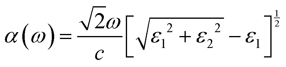
The Vienna ab initio simulation package (VASP)44 was used to study the energy bands and optimization structure of BL borophene. The calculations utilized the Perdew–Burke–Ernzerhof (PBE) functional and generalized-gradient approximation (GGA),45 and the DFT-D3 method was employed to enhance the atomic geometry.46 A vacuum layer in the z direction prevented interlayer interaction. The final force convergence was less than 0.05 eV Å−1, the energy convergence was within 1 × 10⁻⁵ eV, the k-points were 4 × 2 × 1, and the cut-off energy was set to 300 eV.The calculation of optical properties is based on the frequency-dependent dielectric function,
| ε(ω) = ε1(ω) + iε2(ω) | (1) |
 | (2) |
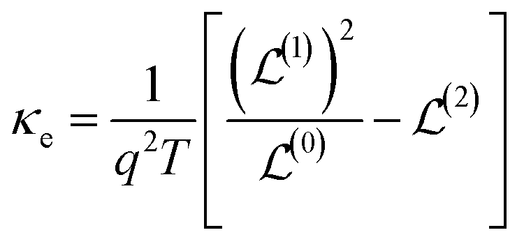
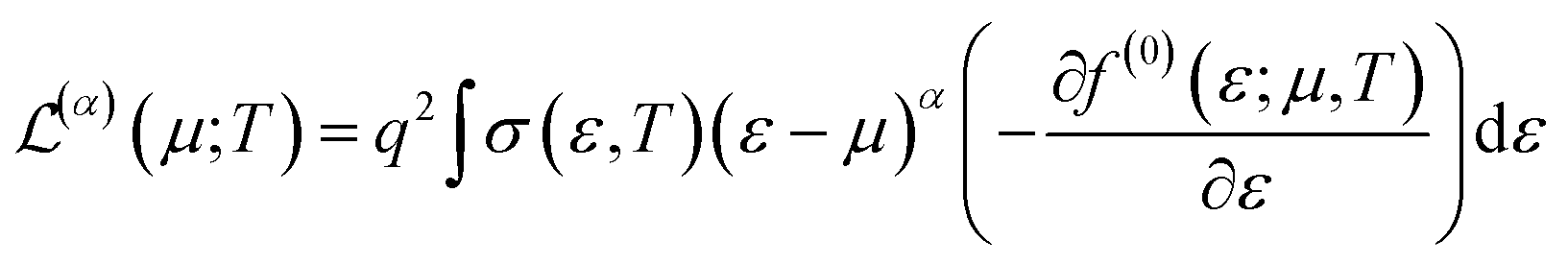
The BoltzTraP2 package48 was used to obtain the thermoelectric properties of BL borophene by solving the Boltzmann transport equation (BTE) with the relaxation time approximation. The Seebeck coefficient (S) and thermal conductivity (κ) can be expressed as:
 | (3) |
 | (4) |
 | (5) |
 | (6) |
 | (7) |
3. Discussion
The top and side views of BL β12-like phase borophene on a Cu(111) substrate are shown in Fig. 1(a) and (b), respectively. The vacancy density of the β12-like phase is 11/72, and the coordination numbers are 4, 5 and 6. The Cu(111) substrate and borophene are formed in the XY plane. The charge distribution at the ground state reveals strong coupling interactions between the Cu(111) substrate and the BL borophene (Fig. 1(c)). The electrons are mainly distributed between Cu(111) and BL borophene, and the holes are distributed in the bottom of the borophene and top layer of Cu atoms. This indicates that the electrons transform from Cu to regions between the Cu(111) surface and borophene layer.37 In this way, the sandwich structure of the hole–electron–hole promotes structural stability and a strong interfacial van der Waals (vdW) interaction exists between the Cu substrate and the interfacial layer of BL borophene. Moreover, the formation of interlayer chemical bonds, facilitated by the transfer of electrons, contributes to the robust interaction observed between the top layer of borophene and the borophene of the interfacial layer. The vdW interaction is also present between the interfacial Cu atoms of a Cu film. As a result of interaction between BL borophene and the Cu substrate, the Cu substrate becomes rough which is caused by the fluctuation of Cu atoms on the surface of Cu substrate. This interaction makes the Cu atoms on the surface of the Cu substrate move around. | ||
| Fig. 1 BL β12-like phase borophene on Cu(111) films, where (a) and (b) are top and side views respectively. (c) Planar-averaged electron density where red and green represent electrons and holes respectively. (d) Electron number density, Laplacian of electron number density, electron energy density and electron localization function of BL borophene (left–right). | ||
As shown in Fig. 1(c), the Cu atoms transfer a huge number of electrons to the borophene layer, resulting in the BL borophene. As shown in Fig. 1(d), the electric density ρ ≫ 0, electronic energy density E < 0, and ∇2ρ < 0 for the interlayer chemical bond BL borophene. This shows that it is a standard covalent bond.51,52 The interlayer distance is 3.7 Å, and the interlayer bond length is 1.8 Å. The interlayer distance of the borophene grown on the Cu(111) film is less than that of BL borophene grown without a Cu substrate in a vacuum. This is due to the attraction between positive and negative charges in the Cu film and the interfacial and top layers of borophene. Fig. 1(d) (right) shows the electronic localization function (ELF) distributions of interlayer bonds, respectively. ELF represents the de-regionalization of the electrons;53,54 the more localized the electron is, the more confined it is and as a result the electrons are less likely to escape. According to the results of the ELF distribution, the Cu substrate forms a stable and strong covalent bond with BL borophene.
Fig. 2(a) and (b) represent the top and side views of charge difference density of BL borophene without a substrate. In the XY plane, electrons and holes exhibit a broken line distribution pattern. Specifically, electrons are predominantly concentrated on the interlayer bonds, while holes are mainly distributed within the borophene layers. This forms a stable hole–electron–hole sandwich structure. The planar-averaged electron density of BL borophene (Fig. 2(c)) also shows a large electron density at the interlayer bond and a large hole density at the borophene layer. The energy bands of BL borophene (Fig. 2(d)) cross the Fermi level, which shows the metallicity of BL β12-like phase borophene.
 | ||
| Fig. 2 (a) and (b) Top and side views of charge difference density of BL borophene without a substrate, (c) planar-averaged electron density, and (d) band structure of BL borophene. | ||
The optical properties of borophene and Cu are essential for applications of sunlight absorption and transition into current for various applications. Its sophisticated dielectric function particularly shows optical properties through eqn (1) and (2). In this work, in terms of the imaginary part ε2(ω), the absorption spectra are calculated at wavelengths between 300 nm and 2400 nm as shown in Fig. 3(a). The dielectric constant of BL borophene is valuable to explore;55,56 its real parts along the x and y-axis are positive in the VR which shows that there is no plasmon effect. Considering the stability and variation of electronic properties of borophene, it is valuable to interrogate the effects of borophene on optical properties, especially the optical absorbance as shown in Fig. 3(b), which shows two absorption peaks along the x and y-axes. One peak is red and the other one is black. The contribution of the y-axis peak is larger in the visible and near-infrared (NIR) regions and in the mid-infrared (MIR) region, the absorption along the x-axis is larger than that along the y-axis, which makes β12-like phase borophene a potential optical sensor. The β12-like phase borophene, synthesized on the Cu(111) film, exhibits remarkable optical properties, characterized by a superior absorption spectrum and dielectric constant, establishing its potential as a highly efficient material for optoelectronic applications. With a unique electronic structure and strong interlayer coupling, the BL borophene demonstrates enhanced light–matter interactions, resulting in exceptional light absorption across a broad range of wavelengths. The absorption spectrum of this material shows a significantly high absorption coefficient, enabling efficient harvesting of incident photons and facilitating the development of high-performance photovoltaic devices. Additionally, the BL borophene exhibits an impressive dielectric constant, reflecting its ability to store and transport electric charges, which holds great promise for the design and fabrication of advanced electronic devices with improved capacitance and charge transport characteristics.57,58
 | ||
| Fig. 3 (a) The dielectric function of BL borophene on a Cu(111) film in the infrared region and visible regions. (b) Optical absorption spectra of BL borophene on a Cu(111) substrate. | ||
Fig. 4(a) illustrates that the characteristics of the I–V curves vary with molecular unit length. Interestingly, the distribution of I–V curves remains symmetrical at both positive and negative bias voltages. As the bias voltage increases, there is a linear growth in current across all molecules until it reaches its initial peak. Subsequently, a Negative Differential Resistance (NDR) effect becomes apparent, leading to a decrease in current. Fig. 4(b) illustrates the voltage-dependent conductance, reflecting the electron transport capacity and aligning with the relationship I = σV in the DC circuit.
 | ||
| Fig. 4 (a) I–V curve over different voltage regions, (b) conductance of device electrical transport over different voltage regions. | ||
In the case of small molecular unit lengths (n ≤ 2), the highest conductance is observed within the range of −0.5 to 0.5 V. Conversely, when dealing with large molecular unit lengths (n ≥ 3), the conductance within the −0.1 to 0.1 V range is significantly lower compared to that at higher bias voltages. Furthermore, around ±0.1 V, the conductance reaches its minimum, serving as a distinct indicator of the transition in transport behavior from shorter to longer molecular unit lengths.
Fig. 5 illustrates the dependency of the photocurrent on optical absorption. In our pursuit of optimizing the photocurrent, we introduce slight bias voltages of 0.1 V and 0.5 V see Fig. 4(a) and (b). The results highlight a remarkable 103-fold enhancement in photocurrent during resonant optical absorption, as visualized in Fig. 5.
 | ||
| Fig. 5 Photocurrent at different linear polarization angles. | ||
Notably, a bias voltage of 0.5 V is recommended, considering the minimal dark current and conductance observed in Fig. 4(a) and (b). This voltage configuration proves to be highly effective in maximizing the desired outcomes while minimizing unwanted electrical interference.
However, it's apparent that the increase in photocurrent intensity, while significant, remains somewhat modest in comparison to resonant optical absorption. This underscores the need for further adjustments in bias voltages to achieve more substantial gains in photocurrent. Therefore, meticulous optimization of the bias voltage settings will play a pivotal role in addressing this challenge and enhancing the overall performance of the device.
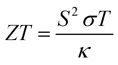
We have studied the uses of BL borophene for thermoelectric devices and its performance can be evaluated by the thermoelectric figure of merit (ZT),
 | (8) |
 | ||
| Fig. 6 Chemical potential and temperature dependent (a) Seebeck coefficient, (b) electrical conductivity, (c) thermal conductivity, (d) thermoelectric figure of merit. | ||
It is intriguing to compare the thermoelectric properties of bilayer borophene synthesized on the Cu(111) film with those reported in our previous theoretical study on the Ag(111) film in ref. 31 (see ESI). According to formula (7), good thermoelectric materials should exhibit large S and σ and small κ. In Fig. 7, it is found that with BL synthesized on the Ag(111) film, the κ is beneficial for ZT, but σ is relatively small in the best region of S at low temperature; when BL is synthesized on the Cu film, the σ is large, and κ is also large for the best region of S at high temperature. In addition, due to the existence of double Dirac points, there is an obvious separation of positive and negative Seebeck coefficients near the determined chemical potential of borophene synthesized on the Ag substrate, and there is no Dirac point in borophene synthesis on the Cu(111) substrate, so the above phenomenon does not exist. Therefore, borophene synthesized on the Ag(111) substrate is suitable for low temperature regions, while borophene synthesized on the Cu(111) substrate is suitable for high temperature regions. Therefore, the choice of metal films can induce variations in the structure of bilayer borophene, and consequently, their distinct geometries and electronic properties contribute to different thermoelectric properties.
 | ||
| Fig. 7 Thermoelectric properties of two different kinds of BL borophene synthesized on Ag(111) and Cu(111) films, respectively. Data from on the Ag film is from ref. 31. | ||
4. Conclusion
In summary, this study has demonstrated the properties of BL borophene, synthesized on a Cu(111) film, as a promising candidate for optoelectronic devices. By analyzing its electronic, thermoelectric, and optical properties, we have gained insight into the physical characteristics of this material. The complex exciton peaks observed in both the IR and visible regions in the optical absorption spectrum highlight its unique optical properties. Moreover, the remarkable thermoelectric properties of bilayer borophene indicate its potential as an efficient energy converter. Overall, our findings highlight that BL borophene has a future in the domain of optoelectronics, with the potential to contribute to the development of high-performance devices.Conflicts of interest
There are no conflicts to declare.Acknowledgements
This work was supported by the National Science Foundation of China (grant no. 11874407, 91436102 and 11374353) and the Fundamental Research Funds for the Central Universities (06500067).References
- K. S. Novoselov, A. K. Geim, S. V. Morozov, D. E. Jiang, Y. Zhang, S. V. Dubonos and A. A. Firsov, Electric field effect in atomically thin carbon films, Science, 2004, 306, 666–669 CrossRef CAS PubMed.
- K. S. Novoselov, A. K. Geim, S. V. Morozov, D. Jiang, M. I. Katsnelson, I. V. Grigorieva and A. Firsov, Two-dimensional gas of massless Dirac fermions in graphene, Nature, 2005, 438, 197–200 CrossRef CAS PubMed.
- D. S. L. Abergel, V. Apalkov, J. Berashevich, K. Ziegler and T. Chakraborty, Properties of graphene: a theoretical perspective, Adv. Phys., 2010, 59, 261–482 CrossRef CAS.
- A. C. Neto, F. Guinea, N. M. Peres, K. S. Novoselov and A. K. Geim, The electronic properties of graphene, Rev. Mod. Phys., 2009, 81, 109 CrossRef.
- K. S. Novoselov, V. I. Falko, L. Colombo, P. R. Gellert, M. G. Schwab and K. Kim, A roadmap for graphene, Nature, 2012, 490, 192–200 CrossRef CAS PubMed.
- K. Kang, K. H. Lee, Y. Han, H. Gao, S. Xie, D. A. Muller and J. Park, Layer-by-layer assembly of two-dimensional materials into wafer-scale heterostructures, Nature, 2017, 550, 229–233 CrossRef PubMed.
- L. Cui, J. Wang and M. Sun, Graphene plasmon for optoelectronics, Rev. Phys., 2021, 6, 100054 CrossRef.
- Z. Zhang, E. S. Penev and B. I. Yakobson, Two-dimensional boron: structures, properties and applications, Chem. Soc. Rev., 2017, 46, 6746–6763 RSC.
- Z. A. Piazza, et al., Planar hexagonal B36 as a potential basis for extended single-atom layer boron sheets, Nat. Commun., 2014, 5(1), 3113 CrossRef PubMed.
- S. Karimzadeh, B. Safaei and T. C. Jen, Investigation on electrochemical performance of striped, β12 and χ3 Borophene as anode materials for lithium-ion batteries, J. Mol. Graphics, 2023, 120, 108423 CrossRef CAS PubMed.
- Z. Xie, X. Meng, X. Li, W. Liang, W. Huang, K. Chen and H. Zhang, Two-dimensional borophene: properties, fabrication, and promising applications, Research, 2020, 2624617 CAS.
- A. Saad, D. Liu, Y. Wu, Z. Song, Y. Li, T. Najam and X. Cai, Ag nanoparticles modified crumpled borophene supported Co3O4 catalyst showing superior oxygen evolution reaction (OER) performance, Appl. Catal., B, 2021, 298, 120529 CrossRef CAS.
- G. Tai, et al., Borophene nanosheets as high-efficiency catalysts for the hydrogen evolution reaction, ACS Appl. Mater. Interfaces, 2021, 13(51), 60987–60994 CrossRef CAS PubMed.
- W. Shao, et al., Stacking and freestanding borophene for lithium-ion battery application, Nanotechnology, 2023, 34(31), 315401 CrossRef PubMed.
- X. Wang, et al., Ultrathin molybdenum boride films for highly efficient catalysis of the hydrogen evolution reaction, J. Mater. Chem. A, 2017, 5(45), 23471–23475 RSC.
- C. Hou, et al., Borophene-based materials for energy, sensors and information storage applications, Nano Res. Energy, 2023, 2(2), e9120051 CrossRef.
- Y. V. Kaneti, D. P. Benu, X. Xu, B. Yuliarto, Y. Yamauchi and D. Golberg, Borophene: Two-dimensional Boron Monolayer: Synthesis, Properties, and Potential Applications, Chem. Rev., 2022, 122, 1000–1051 CrossRef CAS PubMed.
- B. Peng, H. Zhang, H. Shao, Y. Xu, R. Zhang and H. Zhu, The electronic, optical, and thermodynamic properties of borophene from first-principles calculations, J. Mater. Chem. C, 2016, 4, 3592–3598 RSC.
- M. Safari, E. Vesselli, S. de Gironcoli and S. Baroni, Growing borophene on metal substrates: a theoretical study of the role of oxygen on Al(111), Phys. Rev. Mater., 2022, 6, 115801 CrossRef CAS.
- C. Chen, H. Lv, P. Zhang, Z. Zhuo, Y. Wang, C. Ma and L. Chen, Synthesis of bilayer borophene, Nat. Chem., 2022, 14, 25–31 CrossRef CAS PubMed.
- Z. Zhang, Y. Yang, G. Gao and B. I. Yakobson, Two-dimensional boron monolayers mediated by metal substrates, Angew. Chem., 2015, 127, 13214–13218 CrossRef.
- X. Liu, L. Wang, S. Li, M. S. Rahn, B. I. Yakobson and M. C. Hersam, Geometric imaging of borophene polymorphs with functionalized probes, Nat. Commun., 2019, 10, 1642 CrossRef PubMed.
- D. Li, J. Gao, P. Cheng, J. He, Y. Yin, Y. Hu and J. Zhao, 2D boron sheets: structure, growth, and electronic and thermal transport properties, Adv. Funct. Mater., 2020, 30, 1904349 CrossRef CAS.
- M. A. Mohebpour, S. M. Mozvashi, S. I. Vishkayi and M. B. Tagani, Transition from metal to semiconductor by semi-hydrogenation of borophene, Phys. Rev. Mater., 2022, 6, 014012 CrossRef CAS.
- N. A. Vinogradov, A. Lyalin, T. Taketsugu, A. S. Vinogradov and A. Preobrajenski, Single-phase borophene on Ir(111): formation, structure, and decoupling from the support, ACS Nano, 2019, 13, 14511–14518 CrossRef CAS PubMed.
- B. Kiraly, X. Liu, L. Wang, Z. Zhang, A. J. Mannix, B. L. Fisher and N. P. Guisinger, Borophene synthesis on Au(111), ACS Nano, 2019, 13, 3816–3822 CrossRef CAS PubMed.
- X. Liu, Q. Li, Q. Ruan, M. S. Rahn, B. I. Yakobson and M. C. Hersam, Borophene synthesis beyond the single-atomic-layer limit, Nat. Mater., 2022, 21, 35–40 CrossRef CAS PubMed.
- P. Sutter and E. Sutter, Large-scale layer-by-layer synthesis of borophene on Ru(0001), Chem. Mater., 2021, 33, 8838–8843 CrossRef CAS.
- B. Feng, J. Zhang, Q. Zhong, W. Li, S. Li, H. Li and K. Wu, Experimental realization of two-dimensional boron sheets, Nat. Chem., 2016, 8, 563–568 CrossRef CAS PubMed.
- N. A. Vinogradov, A. Lyalin, T. Taketsugu, A. S. Vinogradov and A. Preobrajenski, Single-phase borophene on Ir(111): formation, structure, and decoupling from the support, ACS Nano, 2019, 13, 14511–14518 CrossRef CAS PubMed.
- A. J. Mannix, X. F. Zhou, B. Kiraly, J. D. Wood, D. Alducin, B. D. Myers and N. P. Guisinger, Synthesis of borophenes: anisotropic, two-dimensional boron polymorphs, Science, 2015, 350, 1513–1516 CrossRef CAS PubMed.
- T. Niu and M. Zhou, Bilayer borophene prevails over monolayer counterpart, Nano Today, 2022, 46, 101608 CrossRef CAS.
- Y. Xu, et al., Quasi-freestanding bilayer borophene on Ag(111), Nano Lett., 2022, 22(8), 3488–3494 CrossRef CAS PubMed.
- M. Ebrahimi, The birth of bilayer borophene, Nat. Chem., 2022, 14, 3–4 CrossRef CAS PubMed.
- Y. Xu, X. Xuan, T. Yang, Z. Zhang, S. D. Li and W. Guo, Quasi-freestanding bilayer borophene on Ag(111), Nano Lett., 2022, 22, 3488–3494 CrossRef CAS PubMed.
- M. Ou, X. Wang, L. Yu, C. Liu, W. Tao, X. Ji and L. Mei, The emergence and evolution of borophene, Adv. Sci., 2021, 8, 2001801 CrossRef CAS PubMed.
- Z. Wu, G. Tai, R. Liu, W. Shao, C. Hou and X. Liang, Synthesis of borophene on quartz towards hydroelectric generators, J. Mater. Chem. A, 2022, 10, 8218–8226 RSC.
- R. Yang and M. Sun, Bilayer borophene synthesized on Ag(111) film: physical mechanism and applications for optical sensor and thermoelectric devices, Mater. Today Phys., 2022, 23, 100652 CrossRef CAS.
- P. Cheng, X. Wu, K. Wu and L. Chen, Synthesis of bilayer borophene, Nat. Chem., 2022, 14, 25–31 CrossRef PubMed.
- G. Tai, et al., Synthesis of atomically thin boron films on copper foils, Angew. Chem., Int. Ed., 2015, 54(51), 15473–15477 CrossRef CAS PubMed.
- C. Hou, et al., Ultrastable crystalline semiconducting hydrogenated borophene, Angew. Chem., Int. Ed., 2020, 59(27), 10819–10825 CrossRef CAS PubMed.
- C. Hou, et al., Borophene-graphene heterostructure: preparation and ultrasensitive humidity sensing, Nano Res., 2021, 1–8 CAS.
- C. Hou, et al., Ultrasensitive humidity sensing and the multifunctional applications of borophene–MoS2 heterostructures, J. Mater. Chem. A, 2021, 9(22), 13100–13108 RSC.
- G. Kresse and J. Furthmüller, Efficient iterative schemes for ab initio total-energy calculations using a plane-wave basis set, Phys. Rev. B: Condens. Matter Mater. Phys., 1996, 54, 11169 CrossRef CAS PubMed.
- J. P. Perdew, K. Burke and M. Ernzerhof, Generalized gradient approximation made simple, Phys. Rev. Lett., 1996, 77, 3865 CrossRef CAS PubMed.
- S. Grimme, J. Antony, S. Ehrlich and H. Krieg, A consistent and accurate ab initio parametrization of density functional dispersion correction (DFT-D) for the 94 elements H-Pu, Chem. Phys., 2010, 132, 154104 Search PubMed.
- M. Gajdoš, K. Hummer, G. Kresse, J. Furthmüller and F. Bechstedt, Linear optical properties in the projector-augmented wave methodology, Phys. Rev. B: Condens. Matter Mater. Phys., 2006, 73, 045112 CrossRef.
- G. K. Madsen, J. Carrete and M. J. Verstraete, BoltzTraP2, a program for interpolating band structures and calculating semi-classical transport coefficients, Comput. Phys. Commun., 2018, 231, 140–145 CrossRef CAS.
- J. Song and M. Sun, Challenging breaking thermoelectric performance limits by twistronics, J. Mater. Chem. A, 2023, 11, 13519 RSC.
- J. Song, Y. Cao, J. Dong and M. Sun, Superior Thermoelectric Properties of Twist-Angle Superlattice Borophene Induced by Interlayer Electrons Transport, Small, 2023, 2301348 CrossRef CAS PubMed.
- R. G. Woolley, Quantum theory and molecular structure, Adv. Phys., 1976, 25, 27–52 CrossRef CAS.
- R. McWeeny and B. T. Pickup, Quantum theory of molecular electronic structure, Rep. Prog. Phys., 1980, 43, 1065 CrossRef.
- B. T. Sutcliffe and R. G. Woolley, On the quantum theory of molecules, Chem. Phys., 2012, 137, 22A544 Search PubMed.
- P. Fuentealba, E. Chamorro and J. C. Santos, Chapter 5 Understanding and using the electron localization function, Theoretical Aspects of Chemical Reactivity, Theoretical and Computational Chemistry, Elsevier, 2007, vol. 19, pp. 57–85 Search PubMed.
- V. Tsirelson and A. Stash, Determination of the electron localization function from electron density, Chem. Phys. Lett., 2002, 351, 142–148 CrossRef CAS.
- M. A. Mohebpour, S. M. Mozvashi, S. I. Vishkayi and M. B. Tagani, Transition from metal to semiconductor by semi-hydrogenation of borophene, Phys. Rev. Mater., 2022, 6, 014012 CrossRef CAS.
- S. Jalili and A. Pakzadiyan, Tensile strain as an efficient way to tune transport properties of Graphdiyne/Borophene hetero-bilayers; a first principle investigation, Comput. Mater. Sci., 2023, 224, 112161 CrossRef CAS.
- S. Jing, W. Chen, J. Pan, W. Li, B. Bian, B. Liao and G. Wang, Electronic properties of Borophene/InSe van der Waals heterostructures, Mater. Sci. Semicond. Process., 2022, 146, 106673 CrossRef CAS.
- M. Bhavyashree, S. R. Rondiya and K. Hareesh, Exploring the emerging applications of the advanced 2-dimensional material borophene with its unique properties, RSC Adv., 2022, 12(19), 12166–12192 RSC.
- K. Khan, A. K. Tareen, M. Aslam, M. F. Khan, Z. Shi, C. Ma and Z. Guo, Synthesis, properties and novel electrocatalytic applications of the 2D-borophene Xenes, Prog. Solid State Chem., 2020, 59, 100283 CrossRef CAS.
| This journal is © The Royal Society of Chemistry 2024 |