
 Open Access Article
 This Open Access Article is licensed under a Creative Commons Attribution-Non Commercial 3.0 Unported Licence
Unveiling the nature of room-temperature-fabricated p-type SnO thin films: the critical role of intermediate phases, lattice disorder, and oxygen interstitials†
Mochamad
Januar
 a,
Cheng-Yu
Lu
b,
Horng-Chih
Lin
c,
Tsung-Yu
Huang
*b,
Chia-Ming
Yang
*abdefg,
Kuo-Kang
Liu
h and
Kou-Chen
Liu
*abij
a,
Cheng-Yu
Lu
b,
Horng-Chih
Lin
c,
Tsung-Yu
Huang
*b,
Chia-Ming
Yang
*abdefg,
Kuo-Kang
Liu
h and
Kou-Chen
Liu
*abij
aDepartment of Electronic Engineering, Chang Gung University, Taoyuan 33302, Taiwan. E-mail: cmyang@mail.cgu.edu.tw; jacobliu@mail.cgu.edu.tw
bDepartment of Materials Engineering, Ming Chi University of Technology, New Taipei City 24301, Taiwan. E-mail: huang.tsungyu@mail.mcut.edu.tw
cDepartment of Electronics Engineering and Institute of Electronics, National Yang Ming Chiao Tung University, Hsinchu 300, Taiwan
dInstitute of Electro-Optical Engineering, Chang Gung University, Taoyuan City 33302, Taiwan
eBiosensor Group, Biomedical Engineering Research Center, Chang Gung University, Taoyuan City 33302, Taiwan
fDepartment of General Surgery, Chang Gung Memorial Hospital at Linkou, Taoyuan City 333, Taiwan
gDepartment of Neurosurgery, Chang Gung Memorial Hospital at Linkou, Taoyuan City 333, Taiwan
hSchool of Engineering, University of Warwick, Coventry CV4 7AL, UK
iDivision of Pediatric Infectious Disease, Department of Pediatrics, Chang Gung Memorial Hospital at Linkou, Taoyuan City 333, Taiwan
jHealthy Aging Research Center, Chang Gung University, Taoyuan 33302, Taiwan
First published on 7th March 2024
Abstract
The fabrication of p-type tin monoxide (SnO) thin films at room temperature poses significant challenges for conventional methods, primarily due to the electrically anisotropic nature and metastable phases of SnO. Because of this anisotropy, generating effective hole carriers with optimal mobility in SnO requires meticulous thermal annealing, which is nonetheless constrained by SnO's metastability. In this work, we employ ion-beam-assisted deposition (IBAD) to fabricate p-type SnO thin films at room temperature. These films, with their nanocrystalline structure, demonstrate promising electrical performance with a Hall mobility of 2.67 cm2 V−1 s−1 and hole concentration of 5.94 × 1017 cm−3, notably without the need for annealing treatment. Our investigation has revealed a unique volcano-shaped trend in Hall mobility, and inversely, in carrier concentration in response to variations in the argon flow rate during the IBAD process. This relationship, when correlated with changes in the optical properties, structural phase, and chemical state of the films, is crucial for understanding the origin of p-type conductivity in room-temperature-fabricated SnO films—a topic that remains elusive in the current literature. We observed a direct correlation between enhanced mobility and reduced lattice disorder, as well as a strong association between increasing hole carrier concentration and the formation of oxygen interstitials. We also highlight that the intermediate phase composition plays a vital role in determining the degree of disorder in the SnO film, which is essential for creating transport pathways and the oxygen environment necessary for hole carrier formation. These insights are instrumental in guiding the design and characterization of room-temperature fabricated p-type SnO thin films, thus propelling advancements in the field of large-area, flexible electronics.
1 Introduction
Since their inception in 2004,1 n-type amorphous oxide semiconductors (AOSs), such as amorphous indium–gallium–zinc-oxide, have become prominent in thin-film transistor (TFT) applications, notably in the back-planes of flat-panel displays.2,3 Recently, AOSs have also shown promise as candidates for back-end-of-line transistors in monolithic 3-D integration,4,5 owing to their low-temperature processing compatibility, coupled with crystalline-like high mobility, exceeding 10 cm2 V−1 s−1, and exceptionally low leakage currents.1,6 The high performance of low-temperature-processed AOSs stems from the spherically symmetrical and large-radius metal cations with (n − 1)d10ns0 (n ≥ 5) configurations, which facilitate easy wave-function overlap, electron delocalization, and consequently enhanced electron mobility, irrespective of the microstructure.7 However, the ionic bonding nature of the AOS system presents significant challenges in the design of p-type oxides. Specifically, the valence band maxima, crucial for hole transport, are primarily composed of oxygen 2p orbitals. The strong localization of these orbitals impedes efficient hole carrier transport, leading to reduced channel mobility and inferior p-channel performance in TFTs.8Recently, tin monoxide (SnO), a basic binary oxide with 4d105s2 metal cations, has emerged as one of the leading p-type candidate oxide-based materials. Various experimental techniques: including reactive magnetron sputtering,9–11 atomic layer deposition,12–14 pulsed laser deposition,15–17 e-beam evaporation,18–20 and solution processing,21,22 have successfully demonstrated the feasibility of p-type conductivity in SnO thin films. Additionally, SnO has shown substantial improvements in both p-type and ambipolar TFTs, achieving a maximum field-effect mobility exceeding 10 cm2 V−1 s−1 in p-type TFTs23 and a significant gain in complementary metal–oxide–semiconductor-like inverters utilizing ambipolar SnO TFTs.19 Despite these advancements, achieving p-type conductivity in SnO through room-temperature fabrication remains a significant challenge. High-performance SnO thin films typically require well-crystallized structures, necessitating crystallization annealing at high temperatures.2,3,24 For instance, the highest recorded Hall mobility for SnO thin films is 21.0 cm2 V−1 s−1, achieved in epitaxial SnO using PLD on a (001)-preferred orientation yttria-stabilized zirconia substrate.15 This process demands precise control of growth thermodynamics and kinetics by fine-tuning laser fluence and setting the substrate temperature to 350 °C. However, due to the lower thermodynamic stability of SnO compared to SnO2, there is a risk of overoxidation and/or decomposition into intermediate states, potentially either converting the material to n-type SnO2 or to mixed states with poorer mobility.25,26 As a consequence, the reported hole mobility is predominantly much lower.17,27–30 Moreover, non-annealed nanocrystalline SnO films exhibit even lower mobilities,29,31–33 and in the case of amorphous films, the mobilities are often too low to measure25,34,35 due to increased structural disorders. Therefore, it is crucial to deepen our understanding of the mechanisms involved in p-type SnO thin films, especially when fabricated at room temperature, to enable processes compatible with large-area depositions and flexible substrates.
The realization of p-type conductivity in SnO thin films through room-temperature fabrications primarily hinges on two criteria: achieving the intrinsic generation of hole carriers and the structural qualities essential for high mobility. Typically, meeting these criteria involves the use of a high-temperature annealing process.15,17,27,29 First, hole carriers in SnO are intrinsically generated through the formation of tin vacancies (VSn) and/or oxygen interstitials (Oi).36–38 Therefore, annealing in an oxygen-rich ambient is favorable, as it creates a conducive SnO environment for the development of these intrinsic hole sources.27,29 Second, the tetragonal litharge-type (P4/nmm) crystal structure of SnO, referred to as α-SnO, exhibits pronounced anisotropy due to its layered arrangement along the (001) crystallographic direction, with a van der Waals gap of 2.52 Å separating adjacent tin planes.39 This α-SnO structure leads to an anisotropic effective mass of holes, facilitating more efficient hole carrier movement in the Sn–Sn interlayer orientation over the Sn–O intralayer orientation.40,41 Thus, for higher mobility, the preference is to grow (001)-oriented SnO thin films.15,17,29 However, establishing and characterizing the (001) grain orientation in room-temperature-fabricated SnO films using conventional methods presents significant challenges due to the typical absence of a distinct microcrystalline phase.29,36 In their as-deposited state, these films are likely to lack long-range crystal ordering, which tends to lead to more localized electronic states and reduced charge transport efficiency.34,36,42 Hence, an alternative room-temperature fabrication method for p-type SnO thin films is essential to fulfill the dual requirements of generating hole carriers and attaining the necessary crystal structure for high hole mobility. Furthermore, understanding the p-type conductivity mechanisms in the room-temperature-fabricated SnO films is crucial, as they may differ from those in crystalline forms.31,34,36,42
In this study, we showcase the fabrication of p-type SnO thin films at room temperature using the ion-beam-assisted deposition (IBAD) technique and explore its characteristics to rationalize the design for achieving p-type conduction in SnO with room-temperature processing. In the IBAD system, an electron gun (e-gun) controls the vaporization of Sn metal, while an ion source independently generates the ion flux responsible for oxidizing the Sn vapor.31 This setup allows for independent control of both the vapor deposition rate and the energetic ion-flux conditions, enabling controlled oxidation of metallic Sn at room temperature via an ion-bombardment mechanism.43,44 This method facilitates the fine-tuning of native defects for hole carrier generation, along with establishing the structural arrangement necessary for effective hole carrier transport, all achieved at room temperature. Subsequently, we perform an exhaustive correlation between the electrical and material characteristics to understand the p-type conduction mechanism in the fabricated SnO films. Generally, hole conduction in α-SnO crystals is enabled by complex lone-pair hybridization between O 2p and Sn s- and p-orbitals, which delocalizes the edge of the SnO valence band and provides a hole conduction pathway in the crystal.40,41 However, given that the α-SnO microstructure is typically not completely formed in room-temperature processing,29,31 it is challenging to explain hole concentration and mobility behavior solely through the description of lone-pair hole conduction pathways.34,36 Hence, to characterize the origin of p-type conductivity in IBAD-fabricated SnO films, we investigate the roles played by intermediate phases, electronic structure, lattice disorder, and chemical states in influencing these films’ electrical properties. By examining these factors, we aim to elucidate the nature of room-temperature-fabricated p-type SnO thin films and overcome the limitations that have previously hindered the development of high-performance SnO-based devices.
2 Experimental section
SnO films were deposited on the glass substrates using the IBAD technique with a varying argon (Ar) flow rate and a fixed ion-gun anode voltage of 180 V, anode current of 0.2 A, oxygen flow rates of 1.0 sccm, and e-gun deposition rate of 0.4 Å s−1. Prior to deposition, the glass substrates were immersed in an ultrasonic cleaning system using deionized water, acetone solution, isopropyl alcohol, and deionized water for 15 min each, then dried on a hot plate at 120 °C for 5 min. After the substrates were stored, the IBAD vacuum chamber was evacuated from atmospheric pressure to a base pressure of ∼5 × 10⁻⁶ torr using a mechanical pump followed by a turbo pump. Sn metal vapors were generated by directing the electron beam of the e-gun onto granular Sn metal with an average dimension of 5 × 10 mm2 and a high purity grade of 4N placed in a graphite crucible (15 cc and 37.7 × 17 mm2). The deposition rate was monitored by a quartz crystal using the Telemark 880 model. Oxygen ions were generated using the ion-gun by injecting oxygen gas at a flow rate of 1 sccm, which was then mixed with Ar gas at various flow rates. The thickness of the deposited SnOx films was subsequently measured by using an alpha-step profiler (Surfcorder ET 3000 model from Kosaka Laboratory Ltd).The electrical characterizations of the p-type SnO films were performed via Hall-effect measurement (BioRad HL 5500IU) using the van der Pauw scheme (2 cm × 2 cm) at room temperature. X-Ray diffraction (XRD) measurements, using a diffractometer (PANalytical, X'pert-pro MPD), were performed with Cu Kα radiation. Atomic force microscope (AFM, Bruker Dimension Edge SPM) analysis was employed to investigate the surface morphology and roughness of the SnO films. Additionally, the surface morphology was corroborated using field-emission scanning electron microscopy (FE-SEM, JEOL JSM-7500F). To enhance the FE-SEM images, the samples were coated with Pt using a Pt coater at 20 mA for 35 s. The optical properties of the SnO films were studied using a UV-visible spectrometer (JASCO V-770) in the range of 300–1000 nm. We utilized X-ray photoelectron spectroscopy (XPS, PHI-5000 Versaprobe, ULVAC-PHI Inc.) to elucidate the composition and chemical states in the film. Raman scattering measurements were conducted using a micro-Raman spectrometer (Horiba iHR-550) with a monochromatic green laser at a wavelength of 532 nm and a laser power of 0.85 W. A pure Si wafer served as the calibration reference for the Raman shift at 520.7 cm−1.
3 Results and discussion
3.1 Electrical properties and influence of Ar flow rate
We observe a volcano-shaped evolution in Hall mobility and, inversely, in carrier concentration with changes in the Ar flow rate, as illustrated in Fig. 1. First, the data indicate that reducing the Ar flow rate from 6.2 sccm to 5.8 sccm enhances mobility while simultaneously decreasing hole concentration. Specifically, at the 5.8 sccm, we achieved an average mobility of 2.67 cm2 V−1 s−1 and an average carrier concentration of 5.94 × 1017 cm−3 under as-deposited conditions, without any annealing treatment. Subsequently, a further reduction of the flow rate to 5.6 sccm leads to a noticeable decrease in mobility, accompanied by an increase in hole concentration. It is important to note that the film resistivity, despite its zigzag trend, adheres to the relation , indicating an inversely proportional relationship to both mobility (μp) and carrier concentration (p), as evidenced by the lowest resistivity aligning with the highest carrier mobility. The notably high resistivity of 9.07 Ω cm at a 6.0 sccm Ar flow rate can be attributed to a substantial reduction in carrier concentration, with only a slight compensatory increase in mobility. Consequently, the volcano trend indicates that the optimal electrical performance achieved by the IBAD technique is confined within a relatively narrow operational range, similar to results obtained through magnetron sputtering,10,27,37 pulsed laser deposition,15,16 and atomic layer deposition techniques.12–14 However, our study is distinguished from these methods by the absence of any heat treatment, either during or after the deposition process.
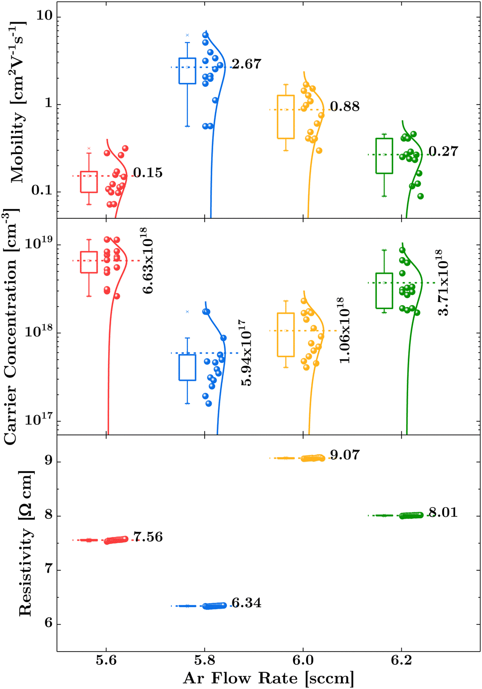 | ||
| Fig. 1 Electrical characteristics. Box-charts showing mobility (upper panel), carrier concentration (middle panel), and resistivity (lower panel) distributions across varying Ar flow rates, based on 15 measurements each. | ||
3.2 Characterizing the nanocrystalline nature of the film: insights from XRD, AFM, and FE-SEM analysis
The XRD analysis was conducted to ascertain the phase structure of the room-temperature fabricated p-type SnO thin films. Regardless of the Ar flow rate conditions, the XRD patterns, as shown in Fig. 2(a), consistently displayed broad diffraction peaks. As summarized in the upper panel of Fig. 2(b), the average grain size, calculated using the Scherrer formula,45 is less than 3.3 nm. A decrease in the Ar flow rate results in a slight increase in grain size, implying that reducing the dilution of Ar in the oxygen ion environment enhances the reaction, facilitating the formation of Sn–O bonds. The information on both the grain size and its evolution is also well corroborated by the surface morphology images obtained from AFM, as shown in Fig. 2(c), where the nanocrystalline grains at the film surface have an average size of less than 4.1 nm, and the trend of their size increases as the Ar flow rate decreases. The AFM images also highlight the benefits of using the room-temperature process, where the RMS surface roughness is low, making it suitable for fabricating large-area devices. These results are consistent with the average nanograin size observed in the FE-SEM images (Fig. 2(d)), which show an increase from 4.1 nm to 4.7 nm as the Ar flow rate decreases from 6.2 sccm to 5.6 sccm. Thus, the broad XRD peaks, the nanometer-scale average grain size, and the surface morphology of the films indicate a minimal presence of long-range crystal ordering, confirming the nanocrystalline nature of the samples.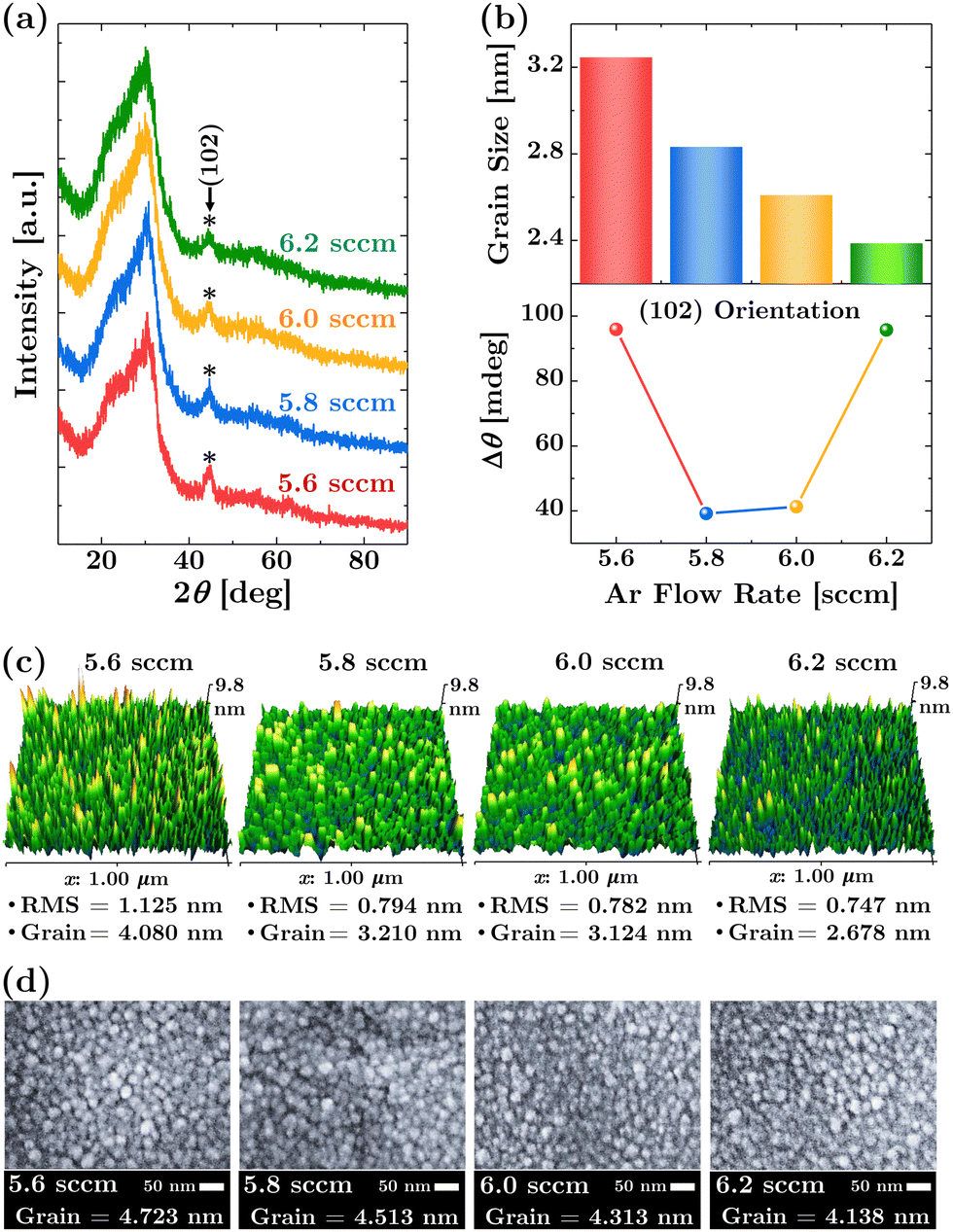 | ||
| Fig. 2 Nanocrystallinity signature in the room-temperature-fabricated SnO film. (a) XRD patterns of the SnOx films plotted as a function of Ar flow rate. (b) Average crystallite size for each sample (upper panel) and angular discrepancy (Δθ) relative to the standard (102)-oriented SnO grains (lower panel). (c) AFM images displaying the surface morphology of the films, highlighting the root-mean-square (RMS) surface roughness and the average grain size. (d) FE-SEM images showing the surface morphology and highlighting the average grain size. | ||
3.3 Lattice ordering and hole carrier mobility
Given the nanocrystalline nature of the p-type SnO thin films, it becomes pertinent to discuss the implications of lattice ordering on hole carrier mobility. Particularly, due to the anisotropic nature of SnO, the higher mobility in these thin films is closely linked to the degree of nanocrystalline order. As demonstrated in previous works,25,34,35 pure amorphous films do not show any p-type conductivity due to their higher structural disorders. Consequently, more ordered nanocrystalline structures facilitate a better-defined lattice arrangement, leading to more efficient hole transportation. In Fig. 2(a), while the XRD patterns are predominantly influenced by the glass substrate, the distinct peak around 44.393° is attributable to the (102)-oriented SnO grains. This orientation is crucial, as it can be used to examine the degree of lattice ordering within the films. Fig. 2(b) (lower panel) offers a comparative analysis of this peak with the standard (102) SnO orientation, as noted in JCPDS card no. 06-0395. Intriguingly, the sample with an Ar flow rate of 5.8 sccm exhibits a peak alignment that more closely mirrors this standard orientation. This suggests a higher degree of lattice ordering in this sample compared to those with different Ar flow rates. Such an enhanced crystalline structure in the 5.8 sccm sample likely contributes to its superior hole carrier mobility.Building on this observation, it is noteworthy to mention that the (102) orientations of SnO are uniquely associated with the (111) Sn face.46 Considering the complex nature of the (111) tin face, it is theorized that an intermediate, two-dimensional, rearranged Sn–O lattice may form between the Sn and the SnO. This could be a response to the difficulty of achieving an intimate fit of the oxide lattice directly onto the metal surface, which would otherwise necessitate excessive strain and distortion of both crystal lattices. The potential existence of such an intermediate lattice structure might play a significant role in determining the observed crystalline order and the associated electronic properties of the films.
3.4 Optical properties and bandgap analysis
Critical insights into the electronic structure and disorder within the SnO films can be derived from their optical properties, characterized using UV-visible spectroscopy. Fig. 3(a) illustrates the band structure of the SnO film, constructed based on the absorption coefficient. This illustration includes fitted functions for extracting both direct and indirect bandgaps following the Tauc method, as well as an exponential function for determining the Urbach energy in accordance with the Urbach rule. For detailed fitting procedures and the link to access the code's user interface for extracting Tauc bandgaps and Urbach energy, refer to Section S1 of the ESI,† eqn (S1)–(S5) and Fig. S1, S2. The Urbach parameter, depicted in pink, represents the exponential decay of tail states at the band edge, known as the Urbach tail. This is indicative of the degree of disorder within the crystal.47 The comparison of the 5.6 sccm and 5.8 sccm samples reveals that the Urbach tail serves as a clear indicator of absorption occurring below the band edge.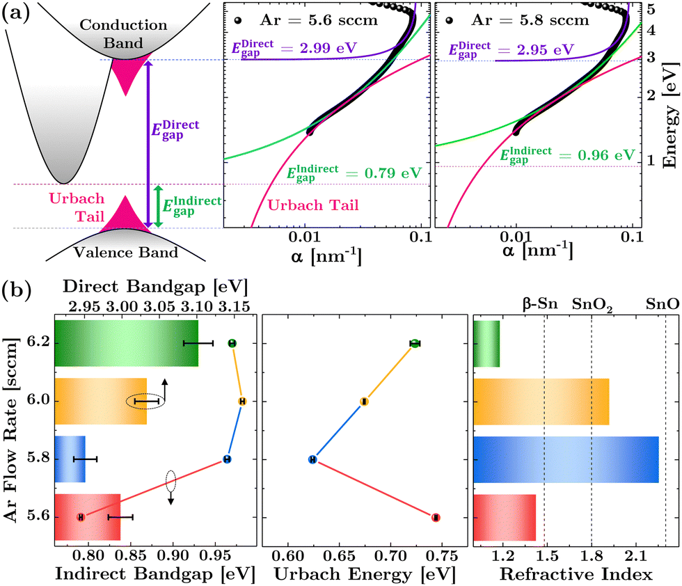 | ||
| Fig. 3 Optical characteristics. (a) Schematic representation of the band structure of the SnO films (left panel), derived from the absorption spectrum, Tauc plot fittings, and analysis of Urbach tails, as demonstrated for the representative cases of 5.6 sccm (middle panel) and 5.8 sccm (right panel) Ar flow rates. (b) Evolution of various optical properties of the SnOx films with changes in Ar flow rates: (left panel) Tauc indirect and direct bandgaps depicted on the left and right axes, respectively, (middle panel) Urbach energy, and (right panel) refractive index at 550 nm. | ||
Fig. 3(b) displays the optical bandgap energy (left panel) and the Urbach energy (middle panel) of the SnO films in relation to variations in the Ar flow rate. Consistent with the electrical characteristics, the trends in both the direct bandgap and Urbach energy inversely align with the volcano-shaped evolution observed in Hall mobility. Reducing the Ar flow rate from 6.2 to 5.8 sccm results in a decreased bandgap, reaching its lowest value of 2.95 eV, which indicates improved oxidation of Sn–O bonds. Given that pure crystalline SnO has a bandgap of 2.8 eV,13,27,48 this lowest direct bandgap is associated with the highest SnO phase purity, suggesting a reduction in defect-related states that act as scattering centers. This inference is supported by the Urbach energy, which also reaches its minimum at 5.8 sccm, signifying the least disorder within the films. This suggests a higher degree of nanocrystallinity and fewer localized states within the bandgap, aligning well with the XRD data. The more ordered material, characterized by fewer defects, leads to more defined optical absorption edges and decreased scattering centers for hole carriers, likely contributing to the highest mobility observed in the film.
The substantial increase in Urbach energy at the lower Ar flow rate of 5.6 sccm, accompanied by a slight increase in the direct bandgap, strongly indicates that the increase in oxygen concentration for the oxidation process has reached saturation. This observation is corroborated by the notable reduction in the indirect bandgap observed for the 5.6 sccm sample, suggesting changes in the phonon-assisted transition energy landscape of the films. These changes might be related to alterations in the phase composition of the films.
3.5 Phase composition and refractive index variation
Insights into the phase composition of SnO films are reflected in their optical properties, particularly in the calculation of their refractive index, n (refer to eqn (S6) and (S7) in Section S2 of the ESI†). Fig. 3(b) (right panel) presents the refractive index values at a wavelength of 550 nm for the films, illustrating how they vary with the Ar flow rate. Aligned with the volcano-shaped evolution observed in other properties, the films exhibit the lowest refractive index of 1.18 at an Ar flow rate of 6.2 sccm. This value gradually increases to 2.25 at an Ar flow rate of 5.8 sccm and then decreases to 1.4 at an Ar flow rate of 5.6 sccm. Previous studies have shown that different phases of tin compounds, such as metallic β-Sn (n ≈ 1.48, see Fig. S3, ESI†) and SnO2 phases (n = 1.7–2.0), exhibit progressively lower refractive indices compared to the SnO phase (n = 2.3–3.0).27 These comparisons are indicated by the vertical dotted line in the figure. Thus, the increase in refractive index with the reduction of the Ar flow rate suggests a strengthening of the SnO phase composition due to improved oxidation, supporting the optical bandgap interpretation. Conversely, the decrease in refractive index at an Ar flow rate of 5.6 sccm implies a reduction in the SnO phase and the emergence of a mixed-phase composition. Hence, the lower refractive indices recorded at Ar flow rates of 5.6 and 6.2 sccm, 1.4 and 1.18 respectively, indicate the presence of significant mixed phases, potentially including Sn metal, the Sn3O4 intermediate phase, and the SnO2 phase.3.6 Chemical state analysis through XPS
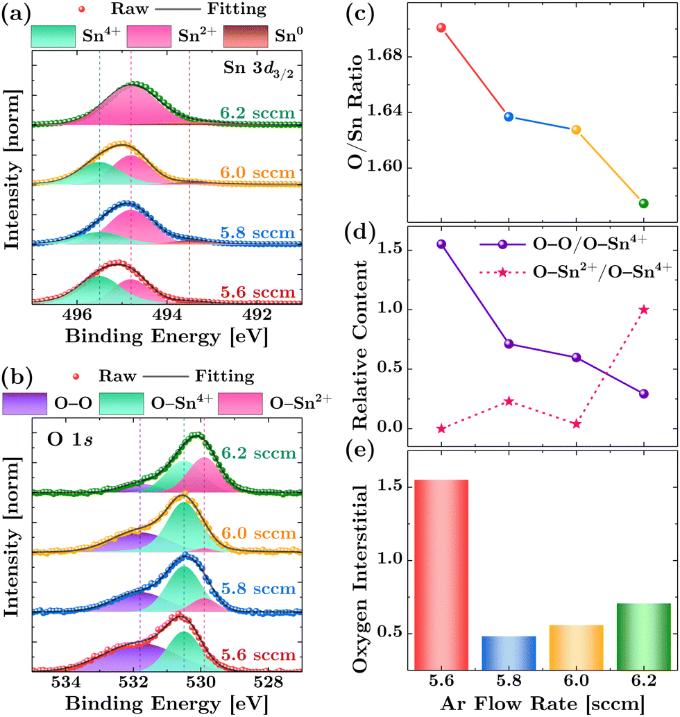
In-depth information on the atomic composition, phase, and chemical states can be obtained using XPS. Prior to analysis, the binding energy position of the XPS spectra was calibrated based on the ISO standard binding energy for isolated metallic gold (Au 4f, 83.96 eV). This calibration involved depositing an approximately 20 nm thin Au film on the top half of the SnO films. The measurements were performed at a point where both Au and SnO signals were sharply detected, as evidenced by the XPS survey scan shown in Fig. S4 (ESI†). As demonstrated in Fig. S5(a) and (b) (ESI†), the calibration was validated after aligning the Au 4f position by checking the C 1s peak positions, which aligned well with the binding energy of adventitious carbon at 284.6 eV.37 Compared to using C 1s alone for calibration, the Au calibration performed better, as the signal remained detectable even after Ar sputtering for depth profile analysis (see Fig. S5(c), ESI†), while the C 1s signal mostly vanished.Fig. 4(a) and (b) show the XPS spectra for the Sn 3d and O 1s orbitals on the SnO film surface, respectively, after performing 1 kV Ar sputtering for 180 s. The data exhibit clear broadening of the spectra, indicating the presence of multiple oxidation states for Sn and O-related bonding. Consequently, the binding energy states of the Sn 3d3/2 core level were deconvoluted into three peaks at 493.5, 494.8, and 495.5 eV, corresponding to Sn0, Sn2+, and Sn4+, respectively.49,50 Additionally, the O 1s peaks were deconvoluted into two components: O–Sn2+ at 529.9 eV and O–Sn4+ at 530.4 eV, along with a peak at 531.7 eV corresponding to O–O bonding oxygen.43,51 This latter peak is assigned considering that, as shown in Fig. 4(c), the films exhibit an O/Sn ratio of over 1.5, indicating an extremely O-rich environment for the SnO films. Consequently, the lattice Sn–O bonds are likely surrounded by a significant amount of oxygen molecules. Furthermore, on surfaces not subjected to Ar sputtering, a prominent higher binding energy peak at 532.55 eV is observed (see Fig. S6, ESI†), which can be attributed to chemisorbed oxygen on the surface or to surface hydroxyl groups.52 For detailed explanations of these two higher binding energy oxygen states, please refer to Section S3.2 of the ESI.†
 | ||
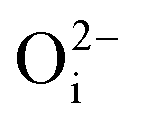
| Fig. 4 Assessment of chemical states and oxygen interstitials. High-resolution spectra of (a) Sn 3d and (b) O 1s orbitals. The as-acquired data points are plotted as circles, the total fitting curve as a solid line, and the deconvoluted spectra for different chemical states as shaded lines. (c) The ratio of the O/Sn atomic concentration of each sample (refer to Tables S1–S4 for detailed elemental atomic percentages of each sample, ESI†). (d) The relative area of the deconvoluted peaks for different oxygen states (O–Sn2+ and O–O bonds) compared to the O–Sn4+ environment. (e) The relative contents of oxygen interstitials in each sample, extracted from the difference between the two oxygen states. | ||
It is worth noting that the highly disordered nanocrystalline nature of the fully room-temperature-fabricated SnO films presents notable challenges for XPS data analysis, more so than with conventional polycrystalline SnO films. This complexity is evident when comparing the deconvolution of valence states in the Sn 3d and O 1s XPS spectra, as shown in Fig. 4(a) and (b). Despite meticulous calibration and efforts to minimize surface oxidation effects through depth profiling analysis, significant discrepancies persist. For instance, in the 6.2 sccm sample analyzed by XPS, the Sn 3d spectrum predominantly indicates the Sn2+ state, with a minor presence of Sn0 and an absence of Sn4+ signals. Conversely, the O 1s spectrum reveals substantial contributions from both O–Sn2+ and O–Sn4+ bonding, alongside a notable O–O peak. The high content of Sn2+ (89.6%) and lack of Sn4+ implies that the film predominantly in the Sn2+ oxidation state, which would ordinarily be expected to favor p-type behavior. However, the nearly equal contributions from O–Sn2+ and O–Sn4+ (43.6%) suggest a significant presence of oxygen environments related to both Sn2+ and Sn4+ states. This could indicate the presence of regions within the film where Sn is not fully coordinated with oxygen, potentially due to the formation of sub-oxides, and hint at a mixed-phase material comprising both SnO and intermediate-phase regions. This scenario aligns with the refractive index values’ implications for the SnO films (Fig. 3(b) (right panel)). Additionally, the balanced presence of O–Sn2+ and O–Sn4+, indicative of a 1![[thin space (1/6-em)]](https://www.rsc.org/images/entities/char_2009.gif) :1 ratio, is echoed in the Raman data, which also shows a 1:1 ratio of coexistence of SnO and Sn3O4-like phases (refer to Section S4 and Fig. S7 of the ESI† for detailed analysis).
:1 ratio, is echoed in the Raman data, which also shows a 1:1 ratio of coexistence of SnO and Sn3O4-like phases (refer to Section S4 and Fig. S7 of the ESI† for detailed analysis).
Moreover, the significant presence of elemental tin (Sn0, 10.4%) supports the notion that some Sn atoms have not been fully oxidized during the deposition process, possibly due to a reduced oxygen environment limiting Sn oxidation at the higher Ar flow rate of 6.2 sccm. The coexistence of Sn0 alongside the previously mentioned mixed oxygen states might contribute to the higher lattice disorder observed in the 6.2 sccm samples, as supported by XRD, surface morphology, and Urbach energy analyses.
3.7 Estimation of oxygen interstitials
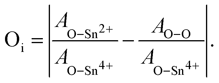
In the context of mixed-phase conditions, we explore the potential origins of hole concentration in nanocrystalline SnOx films. Fig. 4(c) presents a quantitative analysis of the O/Sn atomic ratio, indicating an oxygen-rich environment in the SnO samples. In such oxygen-abundant scenarios, p-type conductivity is commonly attributed to Sn vacancies (VSn) and oxygen interstitials (Oi), as described by the following quasi-chemical stoichiometric reactions:9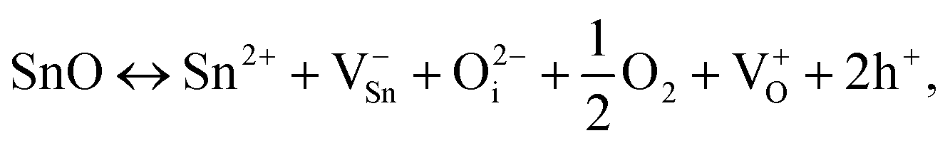 | (1) |
 represents a doubly ionized oxygen interstitial, and V+O signifies a singly ionized oxygen vacancy. In our non-stoichiometric samples, the surplus oxygen may lead to the conversion of some Sn2+ ions into Sn4+ ions for maintaining charge neutrality, especially in the vicinity of ionized Sn2+ ions.53 This conversion can be interpreted as Sn2+ capturing two holes (2h+), resulting in the formation of weakly bonded holes near the top of the valence band, acting as acceptor states. While some theoretical studies have posited that Oi may be electrically inactive,38 the distinct mixed SnOx nanocrystalline nature of our samples requires a unique consideration. This need arises from factors like the numerous interfaces between different phases in the film, an aspect not present in pure crystalline SnO.
In our material, the relative concentration of oxygen interstitials can be inferred by analyzing the chemical states of oxygen, as revealed in the O 1s XPS spectra. As depicted in Fig. 4(c), the O/Sn ratio provides a straightforward macroscopic view of the film's overall oxygen content, which simply increases as the Ar flow rate decreases. Meanwhile, the evolution in the O–Sn2+/O–Sn4+ and O–O/O–Sn4+ ratios in Fig. 4(d) offer insight into the specific oxidation environments and their implications for defect formation. Specifically, the ratio of O–Sn2+/O–Sn4+ offers insights into the relative quantities of oxygen bonded to tin in the +2 and +4 oxidation states, respectively. Additionally, the ratio O–O/O–Sn4+ is hypothesized to represent the proportion of oxygen in interstitial or adsorbed states compared to that bonded to Sn in the +4 state. To isolate and distinguish the contributions of interstitial oxygen from oxygen bonded to Sn, we utilize the following relation:
 | (2) |
Interstitial oxygen in the lattice represents loosely-bound oxygen atoms, distinct from those forming regular Sn–O bonds and free oxygen molecules. This is indicative of structural imperfections within the lattice. Eqn (2) assists in distinguishing the relative amount of oxygen that is neither part of lattice-bound atoms (associated with Sn–O bonds) nor present as free oxygen molecules (O–O). Having quantified the contents of Sn–O bonds and free oxygen molecules in the film through XPS analysis, we are able to estimate the amount of interstitial oxygen in the SnO film. This estimation is achieved by analyzing the difference between the relative presence of lattice oxygen (represented as the ratio of O–Sn2+ to O–Sn4+) and free oxygen molecules (represented as the ratio of O–O to O–Sn4+). Essentially, this difference highlights oxygen atoms that are neither part of the standard lattice structure (SnO or SnO2) nor existing as free molecules. These ‘extra’ atoms, which are not accounted for by regular lattice structures or free oxygen, are likely to be interstitial oxygen, indicating a deviation from the ideal lattice structure and stoichiometric composition. Therefore, this method provides a quantitative estimate of the presence of interstitial-like oxygen in the film.
Fig. 4(e) displays the evolution of this interstitial for each sample, which interestingly parallels the trend observed in the carrier concentration, as determined from the Hall measurement in Fig. 1 (middle panel).
3.8 Raman spectroscopy: structural phase analysis and hole transport
The relative percentage of the coexistence of SnO and Sn3O4 phases in the films can be quantified from Raman spectroscopy. Fig. 5(a) displays the Raman spectra of p-type SnO thin films, specifically acquired in the range of 100–250 cm−1 at room temperature using a 532 nm laser excitation. The prominent peaks in the spectra are at around 110 cm−1, corresponding to the breathing mode of SnO tetrahedra (Eg), and a broader peak at around 210 cm−1, associated with the stretching mode of Sn–O bonds (A1g).27,39,54 Additionally, peaks observed between these two at around 138 cm−1 and 176 cm−1, typically correspond to the formation of Sn3O4-like intermediate phases.31,55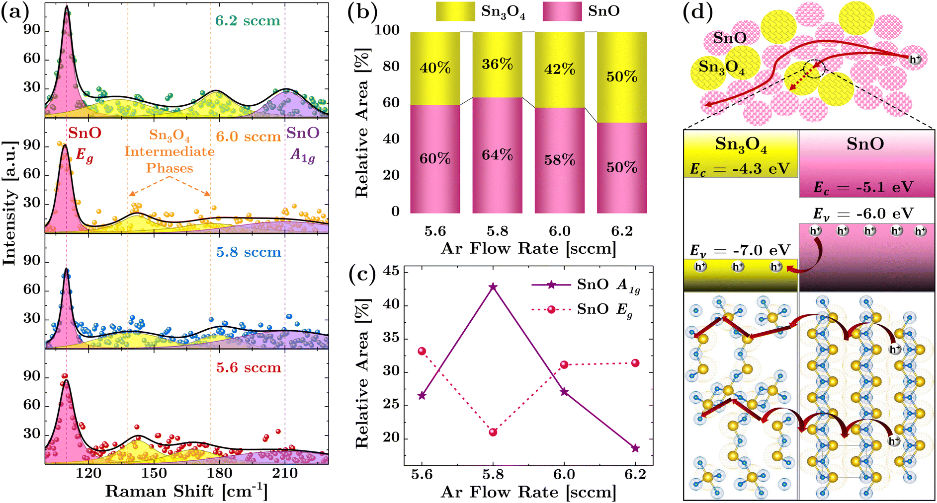 | ||
| Fig. 5 Structural phase analysis and its role for hole transport. (a) Raman spectra of the SnO films as a function of Ar flow rate. (b) Evolution of the deconvoluted peaks representing the SnO Eg, A1g, and Sn3O4-like intermediate modes with changing Ar flow rates. (c) Changes in the relative area of the A1g (∼210 cm−1) and Eg (∼110 cm−1) modes in response to increasing Ar flow rates. (d) Illustration of hole transport occurring through percolation in the SnO phase nanocrystals and transition into the Sn3O4 intermediate phase nanocrystals (upper panel), along with their band diagram arrangement and atomic unit cells illustrating the hole transport between the SnO and Sn3O4 phases (lower panels). | ||
The Raman spectra establish a strong correlation between the p-type mobility of SnO thin films and their phase composition. As shown in Fig. 5(b), higher mobility is observed when the intermediate Sn3O4-like phase is minimized, and the SnO phase becomes more dominant, especially in samples with an Ar flow rate of 5.8 sccm. Fig. 5(c) further elucidates this phenomenon by showing that as the Sn3O4-like intermediate phase decreases in concentration, there is a corresponding increase in the prominence of the SnO A1g mode relative to the SnO Eg modes. Since SnO A1g mode is essentially associated with the stretching of the Sn–O bonds, it is a key indicator of the SnO structural phases present in the films. Hence, the dominance of the SnO A1g mode over SnO Eg mode suggests a shift towards a more SnO-rich phase.
Considering that the SnOx films consist of SnO/Sn3O4-like mixed phases, holes will be transported between the nanocrystals formed by these phases, as illustrated in Fig. 5(d) (top panel). To understand the hole transport mechanism between the SnO and Sn3O4-like phases, we elucidate it based on the concept of band alignment, as depicted in Fig. 5(d) (middle panel). The valence band offset between SnO and Sn3O4 facilitates hole migration into Sn3O4 until the Fermi levels between the two phases equilibrate. The bottom panel of Fig. 5(d) shows that the Sn3O4 unit cell possesses a higher O/Sn ratio compared to SnO unit cell. Consequently, a higher proportion of the Sn3O4-like phase, implying more oxygen interstitials in SnO, enables hole conduction in Sn3O4, albeit with reduced mobility due to more localized states in the Sn3O4-like sites. Conversely, a decrease in the Sn3O4-like phase, particularly at the 5.8 sccm Ar flow rate, leads to a reduction in Oi, thus lowering hole concentration in SnO where enhanced mobility is facilitated by an improved layered structure, resulting in a smaller effective mass of holes.
3.9 Role of film disorder and oxygen interstitials
However, the increase in the intermediate phase alone does not fully explain the abrupt rise in carrier concentration observed at the 5.6 sccm Ar flow rate. The fluctuating Raman shift positions for the intermediate phases, as shown in Fig. 5(a) (yellow peaks), suggest more complex coordination within the film. This complexity may indicate the presence of areas with different oxidation states or phases that are not homogeneously mixed, introducing a variety of defect states. The abrupt reduction in the indirect bandgap for the 5.6 sccm samples, as evidenced in Fig. 3(b), further corroborates the presence of non-homogeneous mixing, which is likely responsible for the observed non-ideal behavior in hole carrier mobility.Therefore, the overall trend in mobility might be related more directly to net film disorder, reflected by the Urbach energy. As depicted in Fig. 6(a), there is a clear alignment between the mobility trend and the Urbach energy. The logarithmic nature of the plot is a consequence of the energy's exponential behavior (see eqn (S2), ESI†), as also seen in the Boltzmann distribution's typical charge-energy relationship.
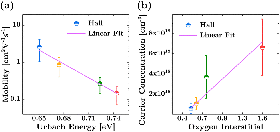 | ||
| Fig. 6 Influence of film disorder and oxygen interstitials in the evolution of Hall mobility and hole concentration. (a) Evolution of Hall mobility in relation to the Urbach energy, reflecting the degree of disorder within the films. (b) Evolution of the hole concentration in relation to the relative concentration of oxygen interstitials. | ||
Furthermore, Fig. 6(b) demonstrates that the increase in the relative concentration of oxygen interstitials correlates well with the rise in hole carrier concentration determined by Hall measurements. This correlation strongly supports the role of oxygen interstitials in generating hole concentration in room-temperature-fabricated SnO thin films.
It is noteworthy that the electrical characteristics of IBAD-fabricated p-type SnO reveal a consistent trend: higher mobility correlates with lower hole concentration. This observation suggests that the primary mechanism governing hole transport in p-type SnO thin films is the scattering of ionized impurities, a notion supported by previous research.15,31,56 In this mechanism, carrier concentration is influenced by the presence of ionized impurities acting as scattering centers, thereby impacting mobility. Specifically, in p-type SnO, hole mobility is contingent upon the concentration of these ionized impurities, which, in this case, can be associated with the concentration of oxygen interstitials. Elevated impurity concentrations lead to increased scattering events, thereby reducing mobility, while decreased concentrations result in fewer scattering events, consequently boosting mobility. This phenomenon is closely tied to the escalation of lattice disorder caused by higher levels of oxygen interstitials resulting from a greater ratio of mixed oxide phases. Thus, the inverse relationship observed between hole mobility and carrier concentration in p-type SnO aligns with the anticipated behavior of the ionized impurity scattering mechanism, highlighting the pivotal role of our findings in delineating the electrical properties of room-temperature-fabricated SnO thin films.
4 Conclusion
In this study, we successfully utilized the IBAD technique to fabricate p-type SnO thin films at room temperature, effectively addressing the challenges associated with SnO's electrically anisotropic nature and metastability. This method distinctively enhances hole mobility without the need for post-annealing, differentiating it from conventional fabrication techniques. We have meticulously elucidated the complex interactions among processing conditions, structural characteristics, oxidation states, and electrical properties in the room-temperature-fabricated SnO films. A pivotal finding is the volcano-shaped evolution of Hall mobility and carrier concentration in response to varying Ar flow rates. This trend is closely associated with changes in (102)-oriented grain ordering, direct bandgap, Urbach energy, refractive index, relative concentration of oxygen interstitials, and Sn3O4-like intermediate phase compositions. Notably, our findings reveal a direct correlation between enhanced mobility and reduced lattice disorder, as well as a strong connection between increased hole carrier concentration and the formation of oxygen interstitials. In conclusion, this study not only underscores the critical role of IBAD as an alternative fabrication technique in determining the structural and electrical properties of SnO films but also provides deeper insights into the mechanisms that drive their p-type behavior. These insights are invaluable for characterizing and optimizing the performance of SnO films in applications such as large-area electronics and flexible devices, where room-temperature fabrication and efficient carrier transport are essential.Conflicts of interest
There are no conflicts to declare.Acknowledgements
This work was supported and funded by the National Science and Technology Council Taiwan Project (112-2221-E-182-045, 109-2221-E-182-063-MY3, and 109-2221-E-182-021-MY3) and the Chang Gung Memorial Hospital Research Project (CMRPD2M0031).Notes and references
- K. Nomura, H. Ohta, A. Takagi, T. Kamiya, M. Hirano and H. Hosono, Nature, 2004, 432, 488–492 CrossRef CAS PubMed.
- A. Nathan and S. Jeon, MRS Bull., 2021, 46, 1028–1036 CrossRef.
- T. Kamiya, K. Nomura and H. Hosono, Sci. Technol. Adv. Mater., 2010, 11, 044305–044327 CrossRef PubMed.
- Y. Son, B. Frost, Y. Zhao and R. L. Peterson, Nat. Electron., 2019, 2, 540–548 CrossRef CAS.
- W. Wang, K. Li, J. Lan, M. Shen, Z. Wang, X. Feng, H. Yu, K. Chen, J. Li, F. Zhou, L. Lin, P. Zhang and Y. Li, Nat. Commun., 2023, 14, 6079–6089 CrossRef CAS PubMed.
- J. Sheng, T. Hong, H.-M. Lee, K. Kim, M. Sasase, J. Kim, H. Hosono and J.-S. Park, ACS Appl. Mater. Interfaces, 2019, 11, 40300–40309 CrossRef CAS PubMed.
- H. Hosono, J. Non-Cryst. Solids, 2006, 352, 851–858 CrossRef CAS.
- H. Kawazoe, M. Yasukawa, H. Hyodo, M. Kurita, H. Yanagi and H. Hosono, Nature, 1997, 389, 939–942 CrossRef CAS.
- E. Fortunato, R. Barros, P. Barquinha, V. Figueiredo, S.-H. K. Park, C.-S. Hwang and R. Martins, Appl. Phys. Lett., 2010, 97, 052105–052107 CrossRef.
- J. A. Caraveo-Frescas, P. K. Nayak, H. A. Al-Jawhari, D. B. Granato, U. Schwingenschlögl and H. N. Alshareef, ACS Nano, 2013, 7, 5160–5167 CrossRef CAS PubMed.
- Z. Wang, P. K. Nayak, A. Albar, N. Wei, U. Schwingenschlögl and H. N. Alshareef, Adv. Mater. Interfaces, 2015, 2, 1500374 CrossRef.
- H.-M. Kim, S.-H. Choi, H. U. Lee, S. B. Cho and J.-S. Park, Adv. Electron. Mater., 2023, 9, 2201202 CrossRef CAS.
- D. E. Gomersall, K. M. Niang, J. D. Parish, Z. Sun, A. L. Johnson, J. L. MacManus-Driscoll and A. J. Flewitt, J. Mater. Chem. C, 2023, 11, 5740–5749 RSC.
- A. Mameli, J. D. Parish, T. Dogan, G. Gelinck, M. W. Snook, A. J. Straiton, A. L. Johnson and A. J. Kronemeijer, Adv. Mater. Interfaces, 2022, 9, 2101278 CrossRef CAS.
- M. Minohara, A. Samizo, N. Kikuchi, K. K. Bando, Y. Yoshida and Y. Aiura, J. Phys. Chem. C, 2020, 124, 1755–1760 CrossRef CAS.
- M. Minohara, N. Kikuchi, Y. Yoshida, H. Kumigashira and Y. Aiura, J. Mater. Chem. C, 2019, 7, 6332–6336 RSC.
- Y. Ogo, H. Hiramatsu, K. Nomura, H. Yanagi, T. Kamiya, M. Hirano and H. Hosono, Appl. Phys. Lett., 2008, 93, 032113 CrossRef.
- Q. Liu, L. Liang, H. Cao, H. Luo, H. Zhang, J. Li, X. Li and F. Deng, J. Mater. Chem. C, 2015, 3, 1077–1081 RSC.
- L. Y. Liang, H. T. Cao, X. B. Chen, Z. M. Liu, F. Zhuge, H. Luo, J. Li, Y. C. Lu and W. Lu, Appl. Phys. Lett., 2012, 100, 263502 CrossRef.
- J. Geurts, S. Rau, W. Richter and F. Schmitte, Thin Solid Films, 1984, 121, 217–225 CrossRef CAS.
- S. A. Miller, P. Gorai, U. Aydemir, T. O. Mason, V. Stevanović, E. S. Toberer and G. J. Snyder, J. Mater. Chem. C, 2017, 5, 8854–8861 RSC.
- K. Okamura, B. Nasr, R. A. Brand and H. Hahn, J. Mater. Chem., 2012, 22, 4607 RSC.
- J. A. Caraveo-Frescas and H. N. Alshareef, Appl. Phys. Lett., 2013, 103, 222103 CrossRef.
- E. Fortunato, P. Barquinha and R. Martins, Adv. Mater., 2012, 24, 2945–2986 CrossRef CAS PubMed.
- L. Y. Liang, Z. M. Liu, H. T. Cao, Z. Yu, Y. Y. Shi, A. H. Chen, H. Z. Zhang, Y. Q. Fang and X. L. Sun, J. Electrochem. Soc., 2010, 157, H598 CrossRef CAS.
- H. Giefers, F. Porsch and G. Wortmann, Solid State Ionics, 2005, 176, 199–207 CrossRef CAS.
- H. Luo, L. Y. Liang, H. T. Cao, Z. M. Liu and F. Zhuge, ACS Appl. Mater. Interfaces, 2012, 4, 5673–5677 CrossRef CAS PubMed.
- T. Toyama, Y. Seo, T. Konishi, H. Okamoto and Y. Tsutsumi, Appl. Phys. Express, 2011, 4, 071101 CrossRef.
- W. Guo, L. Fu, Y. Zhang, K. Zhang, L. Y. Liang, Z. M. Liu, H. T. Cao and X. Q. Pan, Appl. Phys. Lett., 2010, 96, 042113 CrossRef.
- Y. Ogo, H. Hiramatsu, K. Nomura, H. Yanagi, T. Kamiya, M. Kimura, M. Hirano and H. Hosono, Phys. Status Solidi A, 2009, 206, 2187–2191 CrossRef CAS.
- M. Januar, S. P. Prakoso, C.-W. Zhong, H.-C. Lin, C. Li, J.-H. Hsieh, K.-K. Liu and K.-C. Liu, ACS Appl. Mater. Interfaces, 2022, 14, 46726–46737 CrossRef CAS PubMed.
- J. Jung, S. Park, J. Ye, J. Woo, B. Bae and E.-J. Yun, Thin Solid Films, 2022, 747, 139139 CrossRef CAS.
- T. Yang, J. Zhao, X. Li, X. Gao, C. Xue, Y. Wu and R. Tai, Mater. Lett., 2015, 139, 39–41 CrossRef CAS.
- M. J. Wahila, K. T. Butler, Z. W. Lebens-Higgins, C. H. Hendon, A. S. Nandur, R. E. Treharne, N. F. Quackenbush, S. Sallis, K. Mason, H. Paik, D. G. Schlom, J. C. Woicik, J. Guo, D. A. Arena, B. E. White, G. W. Watson, A. Walsh and L. F. J. Piper, Chem. Mater., 2016, 28, 4706–4713 CrossRef CAS.
- H. Yabuta, N. Kaji, R. Hayashi, H. Kumomi, K. Nomura, T. Kamiya, M. Hirano and H. Hosono, Appl. Phys. Lett., 2010, 97, 072111 CrossRef.
- J. Jia, T. Sugane, S.-I. Nakamura and Y. Shigesato, J. Appl. Phys., 2020, 127, 185703 CrossRef CAS.
- S. J. Lee, Y. Jang, H. J. Kim, E. S. Hwang, S. M. Jeon, J. S. Kim, T. Moon, K.-T. Jang, Y.-C. Joo, D.-Y. Cho and C. S. Hwang, ACS Appl. Mater. Interfaces, 2018, 10, 3810–3821 CrossRef CAS PubMed.
- J. B. Varley, A. Schleife, A. Janotti and C. G. Van de Walle, Appl. Phys. Lett., 2013, 103, 082118 CrossRef.
- Y. Duan, Phys. Rev. B: Condens. Matter Mater. Phys., 2008, 77, 045332 CrossRef.
- Y. Hu, D. Schlom, S. Datta and K. Cho, ACS Appl. Mater. Interfaces, 2022, 14, 25670–25679 CrossRef CAS PubMed.
- A. Togo, F. Oba, I. Tanaka and K. Tatsumi, Phys. Rev. B: Condens. Matter Mater. Phys., 2006, 74, 195128 CrossRef.
- S. Husein, J. E. Medvedeva, J. D. Perkins and M. I. Bertoni, Chem. Mater., 2020, 32, 6444–6455 CrossRef CAS.
- W. Choi, H. Jung and S. Koh, J. Vac. Sci. Technol., A, 1996, 14, 359–366 CrossRef CAS.
- W. Choi, J. Cho, S. Song, H.-J. Jung, S. Koh, K. Yoon, C. Lee, M. Sung and K. Jeong, Thin Solid Films, 1997, 304, 85–97 CrossRef CAS.
- A. L. Patterson, Phys. Rev., 1939, 56, 978–982 CrossRef CAS.
- W. E. Boggs, R. H. Kachik and G. E. Pellissier, J. Electrochem. Soc., 1964, 111, 636 CrossRef CAS.
- T.-C. Fung, C.-S. Chuang, K. Nomura, H.-P. D. Shieh, H. Hosono and J. Kanicki, J. Inf. Disp., 2008, 9, 21–29 CrossRef.
- A. Nikiforov, V. Timofeev, V. Mashanov, I. Azarov, I. Loshkarev, V. Volodin, D. Gulyaev, I. Chetyrin and I. Korolkov, Appl. Surf. Sci., 2020, 512, 145735 CrossRef CAS.
- N. F. Quackenbush, J. P. Allen, D. O. Scanlon, S. Sallis, J. A. Hewlett, A. S. Nandur, B. Chen, K. E. Smith, C. Weiland, D. A. Fischer, J. C. Woicik, B. E. White, G. W. Watson and L. F. J. Piper, Chem. Mater., 2013, 25, 3114–3123 CrossRef CAS.
- L. Kovér, Z. Kovács, R. Sanjinés, G. Moretti, I. Cserny, G. Margaritondo, J. Pálinkás and H. Adachi, Surf. Interface Anal., 1995, 23, 461–466 CrossRef.
- V. Jiménez, J. Mejías, J. Espinós and A. González-Elipe, Surf. Sci., 1996, 366, 545–555 CrossRef.
- Z. Zhu, Z. Li, X. Xiong, X. Hu, X. Wang, N. Li, T. Jin and Y. Chen, J. Alloys Compd., 2022, 906, 164316 CrossRef CAS.
- C.-W. Ou, Dhananjay, Z. Y. Ho, Y.-C. Chuang, S.-S. Cheng, M.-C. Wu, K.-C. Ho and C.-W. Chu, Appl. Phys. Lett., 2008, 92, 122113 CrossRef.
- L. Liu, X. Wu, T. Li and J. Shen, Appl. Surf. Sci., 2015, 347, 265–268 CrossRef CAS.
- A. Shanmugasundaram, P. Basak, L. Satyanarayana and S. V. Manorama, Sens. Actuators, B, 2013, 185, 265–273 CrossRef CAS.
- D. Chattopadhyay and H. J. Queisser, Rev. Mod. Phys., 1981, 53, 745–768 CrossRef CAS.
Footnote |
| † Electronic supplementary information (ESI) available: Detailed procedures for the Tauc method, Urbach method, Tauc–Urbach extraction user-interface link, and refractive index calculations, as well as the XPS survey scan of composition, calibration for XPS, XPS spectra at the film surface, and elemental atomic percentages pre- and post-1 kV Ar sputtering for 180 s, as described in the text. See DOI: https://doi.org/10.1039/d3ma01119d |
| This journal is © The Royal Society of Chemistry 2024 |