DOI:
10.1039/D3MA01044A
(Paper)
Mater. Adv., 2024,
5, 3379-3395
Temperature dependent Raman and photoresponse studies of Bi2Te3 thin films annealed at different temperatures for improved optoelectronic performance†
Received
23rd November 2023
, Accepted 25th February 2024
First published on 27th February 2024
Abstract
Nanocrystalline Bi2Te3 thin films of 800 nm thickness synthesized via a thermal evaporation method were annealed at various temperatures, which induced notable changes in both structural and optical characteristics. Structural analysis confirmed the presence of the rhombohedral Bi2Te3 phase in the material. The crystallinity got enhanced at increased annealing temperature. Temperature-dependent Raman studies revealed a red shift in the vibrational modes. Photoluminescence data revealed a blue shift of the emission edge, primarily attributed to the annealing-induced alteration in crystallinity, resulting in greater electron–hole emission efficiency. Morphological analysis provides insights into the slight agglomeration of the films at higher annealing temperatures. The uniform distribution of constituent elements in the films was confirmed through EDX and surface mapping. The optical study indicated a reduction in transmittance values, with increase in the absorption coefficient. The red shift of the absorption edge implied a decrease in the direct optical bandgap value from 0.528 to 0.506 eV. The estimated static refractive index and linear dielectric constant exhibited an increasing trend at higher annealing temperatures. The enhanced non-linear refractive index ranging from 3.62 × 10⁻⁹ to 3.96 × 10⁻⁹ esu resulted in the increase in non-linear susceptibility with annealing. Surface wettability studies demonstrated high hydrophilicity at increased annealing temperature. Photo-response studies indicated an increment in the photo-current for higher temperature annealed films. The observed optimized properties of the films are suitable for various optoelectronic applications, such as absorber layers for solar cells, infrared related devices, and other photo-response applications.
1. Introduction
Recently, semiconducting thin films based on chalcogenides have emerged as prominent candidates for a diverse array of applications in optoelectronics, electronics, and energy-related fields.1,2 Their extensive range of properties have led to their utilization in microelectronics and various coating materials. Among materials based on group V and VI elements, including bismuth selenide (Bi2Se3), bismuth telluride (Bi2Te3), and bismuth sulphide (Bi2S3), Bi2Te3 stands out as an established material, particularly renowned for its thermoelectric properties at room temperature.3–5 Bi2Te3, due to its unique material characteristics, has been pivotal in the development of thermoelectric generators and coolers. Its thin films possess a layered crystalline structure, comprised of quintuple layers of Bi2Te3 units. This unique structure plays a crucial role in their thermoelectric behaviour, significantly impacting their charge transport properties and ultimately contributing to their excellent thermoelectric performance.6 Apart from their thermoelectric prowess, Bi2Te3 thin films exhibit intriguing optical properties driven by their distinctive electronic band structure and quantum confinement effects. Bi2Te3 is classified as a topological insulator, due to its unique electronic band structure. The bandgap of Bi2Te3 thin films falls within the mid-infrared range.7,8 Bi2Te3 thin films display strong absorption within their optical bandgap, a property advantageous for infrared detectors. Their efficient absorption of specific wavelengths of light makes them suitable for applications in thermal radiation sensing and other optical detection technologies.9 Furthermore, the ability to modulate their optical properties upon application of external stimuli, like temperature and electric field, enhances their utility in photonic devices. Due to their mid-infrared absorption capabilities, Bi2Te3 thin films serve as effective materials for infrared photodetectors. They can efficiently convert incident infrared radiation into electrical signals, offering potential applications in thermal imaging, remote sensing, and other fields.10
Various external energy treatments have produced notable modifications in the thin film, for different application purposes. Photoinduced conversion, thermal annealing, ion irradiation, etc. are considered as different energy treatments for many prepared thin films.11–13 Among these, thermal annealing is a widely employed post-deposition process that induces structural, chemical, and physical changes in thin films.14 It is essential for tailoring the properties and enhancing the performance of thin film materials in various applications. Thermal annealing has the potential for the recrystallization and refinement of crystal structure within thin films. It can help eliminate defects, grain boundaries, and dislocations, resulting in larger and more ordered crystal grains.15 This structural enhancement can significantly improve the electrical, optical, and mechanical properties of films. Annealing can promote surface diffusion and smoothen the roughness of thin films, making them more suitable for applications that require precise surface topography, such as integrated circuits and optical coatings.16,17
Several pioneering studies have investigated the transformative effects of annealing on Bi2Te3 thin films, revealing enhancements in their structural, optical, and electrical characteristics. These studies have utilized various deposition methods and annealing techniques to tailor the properties of Bi2Te3 thin films, paving the way for diverse applications. Zheng et al.18 explored the influence of rapid heat treatment on Bi2Te3 films, prepared on polymer substrates using single-source evaporation. The process led to improved crystallinity and controlled grain size, resulting in the dominance of the pure Bi2Te3 phase. This enhancement in crystal quality was reflected in an elevated power factor and a notable increase in the ZT value, highlighting the significance of rapid annealing in optimizing thermoelectric performance. Norimasa et al.19 focused on radio-frequency magnetron sputtering based Bi2Te3 films prepared on polyimide substrates. Post-annealing enhanced the crystallite size and crystal orientation, positively influencing electrical conductivity. However, it also caused substrate stretching, mitigating strain accumulation in the films and promoting crystal growth. This study sheds light on the complex interplay between annealing, substrate, and film properties. Guo et al.20 introduced a scalable method for obtaining high-quality Bi2Te3 films using magnetron sputtering. The enhanced annealing conditions facilitated the formation of large size grains with a smooth surface and highly oriented Bi2Te3 films. This study emphasized the temperature-dependent nature of film growth and its implications for film quality. He et al.21 investigated the in situ annealing of n-type Bi2Te3 films during magnetic sputtering. The study revealed that higher sputtering power led to an increased grain size but reduced electrical conductivity, along with a decrease in carrier concentration. This work demonstrated the intricate relationship between annealing, sputtering conditions and film properties. Naumochkin et al.22 reported the influence of annealing on sputtered Bi2Te3 thin films, highlighting its role in improving crystallinity and reducing defect states. This work underscored the significance of annealing in enhancing film quality and performance. Fan et al. adopted a rapid laser annealing method to produce Bi2Te3 films with superior structural, chemical, and thermoelectric properties compared to those achieved using conventional annealing techniques.23 This innovative approach showcased the potential of advanced annealing methods in tailoring materials' properties. Eguchi et al.24 synthesized Bi2Te3 thin films through the electrodeposition method, observing a crystalline phase transition from Bi2Te3 to Bi4Te5 during annealing. This transition led to an increase in thermoelectric performance, highlighting the role of annealing in modifying the material's composition and properties. Electron-beam synthesis of Te-rich Bi2Te3 thin films at room temperature, followed by annealing at various temperatures, resulted in n-type semiconductor behavior and improved electrical properties.25 Adam et al.26 have reported the optical behaviour of Bi2Te3 films prepared through various techniques such as vacuum thermal evaporation and pulsed laser deposition. The direct optical bandgaps of 0.91 and 0.95 eV were found for films prepared through vacuum and pulsed laser deposition methods, respectively. These two methods exhibit quite different results from each other in terms of optical, structural, and other properties. Jian et al.27 observed modification in the wettability and nanomechanical behaviour of Bi2Te3 films after annealing. Bi2Te3 films deposited by a pulsed laser method over the SiO2/Si substrate showed increased crystallinity, but decreased hardness. Similarly, the contact angle decreased with increasing annealing temperature, which increased the surface energy of the material. The increment in the hydrophilicity occurs due to the increased surface roughness of the material upon annealing. Bi2Te3 materials have evolved to become versatile materials with profound implications for modern optoelectronics, electronics, and energy-related applications. Their unique properties, both in the thermoelectric and optical domains, continue to fuel research and innovation across a range of technological fields. Owing to the importance of Bi2Te3 films in different application sectors based on their unique properties, our aim is to optimize their optoelectronic properties upon thermal annealing and investigate their surface wettability and photo-response behaviour under different annealing conditions.
In the current study, the profound effect of annealing process on thermally evaporated Bi2Te3 thin films was studied thoroughly. By subjecting the as-prepared Bi2Te3 films to annealing at various temperatures, specifically at 473 K (200 °C) and 523 K (250 °C), various alterations in their optical, microstructural, and morphological properties are investigated. The as-grown and annealed films were studied for their structural change by temperature dependent Raman and X-ray diffraction (XRD) analyses. Photoluminescence data were recorded for investigating the shift of emission edge upon annealing.
The contact angle measurement reveals the surface wettability nature, while the photocurrent–voltage response was recorded using a Keithley 2450 meter. The change in optical properties was determined from the UV-visible data, while the elemental composition was determined from the energy dispersive X-ray study (EDX). Transmission electron microscopy (TEM) and field emission scanning electron microscopy (FESEM) were used to observe the surface structural change due to annealing.
2. Synthesis and characterization procedures
2.1. Thin film preparation
Bi2Te3 films were fabricated using the thermal evaporation process with an HHV Smart Coat: 3.0 coating unit. High-purity Bi2Te3 powder (99.999%, Sigma Aldrich) was employed for the synthesis. Prior to film preparation, the glass substrate was cleaned properly with dilute HNO3, aqueous NaOH, and distilled water. The drying of the substrates was done at 373 K (100 °C) inside a hot air oven. Using molybdenum boats, the requisite Bi2Te3 powder samples were loaded into the deposition chamber. The material was deposited to a thickness of approximately 800 nm on the glass substrates. The room temperature conditions and the pressure of 5 × 10⁻⁵ torr within the deposition chamber were maintained. To ensure even and uniform deposition, the substrate holder was in continuous motion at a slow speed. The attached quartz crystal thickness controller monitored the film thickness. Thermal annealing was done for the prepared films at 473 K and 523 K for 2 h in a vacuum oven. Scheme 1 presents the schematic representation of the deposition and thermal annealing of the Bi2Te3 thin film.
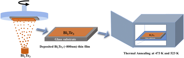 |
| | Scheme 1 Schematic representation of deposition and annealing processes of Bi2Te3 thin films. | |
2.2. Characterisation
XRD data were recorded for the as-grown and annealed Bi2Te3 films using a Bruker D8 Advance machine equipped with a Cu Kα X-ray source (wavelength = 1.54 Å). The operating voltage of 30 kV and current of 40 mA were the operating conditions for XRD. The scan was taken over angles ranging from 20° to 60° at a glancing angle of 1° to obtain the structural information. In addition to XRD, temperature dependent Raman and photoluminescence (PL) measurements have also been done using a Renishaw, RE 04 spectrometer equipped with a 532 nm excitation green laser. Optical measurements were performed using a JASCO-660 UV-vis-NIR spectrophotometer over the wavelength range of 1600–2500 nm with a spectral resolution of 1 nm. The morphology and composition of Bi2Te3 films were determined by using a JEOL, JSM-7601FPLUS FESEM with an attached EDX setup. The FESEM instrument was operated at voltages between 20 and 200 kV during characterization. High-resolution TEM (JEM-2100-HRTEM) was used to estimate the inter-planar spacing and determine the phase composition. The line spacing was accurately calculated from selected area electron diffraction (SAED) and HRTEM images. TEM characterisation was done on the 523 K annealed thin films. The surface wettability test was performed using a DME-211 Plus contact angle measurement unit.
2.3. Photo-response measurement
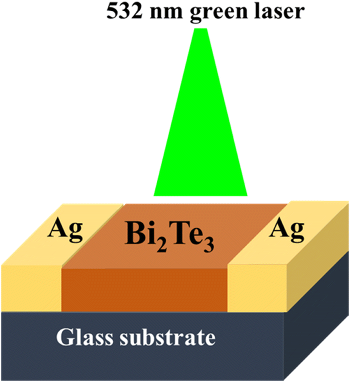
To obtain the photo-current data, both the as-grown and annealed films were deposited on substrates of 5 × 5 mm2 area. To establish conductive contact, a small quantity of Ag paste was applied to the two parallel sides of the films. These samples were then affixed to a sample holder at room temperature. For the photo-response measurement, the materials were illuminated by the 532 nm green laser. Scheme 2 presents the photocurrent measurement set up for the current thin films. The photo-response study was carried out by varying the laser power over the material. Current measurements were performed using a Keithley 2450 meter across a specific voltage varying from −10 V to 10 V. The step size was 0.03 V.
 |
| | Scheme 2 Schematic representation of the photo-current measurement set up. | |
Current–voltage measurements were performed under two distinct conditions: light conditions and dark conditions. Under light conditions, measurements were performed by illuminating the sample with laser powers of 20 mW, 40 mW and 60 mW, respectively. Under dark conditions, measurements were performed with the sample placed under complete darkness. This dual approach allowed for a comprehensive assessment of the sample's response to varying voltage levels in both illuminated and non-illuminated states. On the other hand, the variation of photo-response of the material with time was also determined through the current versus time plot at a particular bias voltage under different laser power conditions.
3. Results and discussion
3.1. XRD analysis
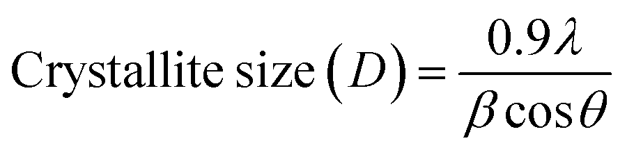
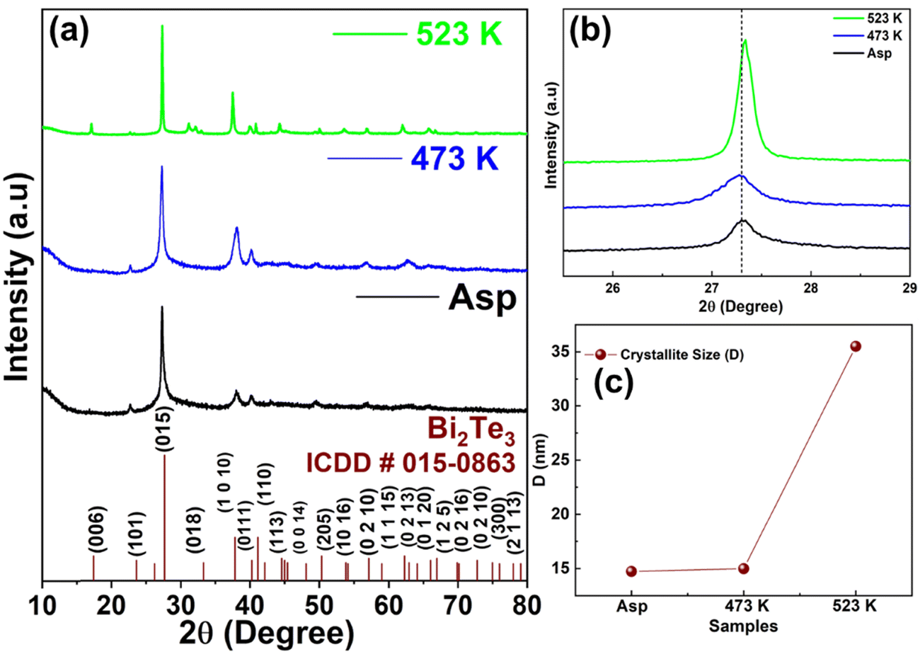
Fig. 1(a) illustrates the XRD pattern of as-grown and annealed Bi2Te3 films showing the formation of rhombohedral phase. The XRD pattern showed the rhombohedral phase (ICDD code: 00-015-0863) of Bi2Te3 films. For the as-grown Bi2Te3 film, the diffraction peaks found around 23.64°, 27.62°, 37.79°, 40.20°, 49.82° and 56.98° correspond to the (hkl) values of (1 0 1), (0 1 5), (1 0 10), (0 1 11), (2 0 5) and (0 2 10), respectively. Meanwhile, the 473 K annealed thin film exhibits a similar pattern to that of the as-prepared thin film, but one more peak at 62.91°, which corresponds to (hkl) (0 2 13). However, the 523 K annealed Bi2Te3 thin film shows greater crystallinity as compared to 473 K annealed and as-grown films. Several other diffraction peaks appeared for the higher temperature annealed films. Peaks around 17.48°, 32.97°, 41.04°, 44.33°, 53.75°, 61.99°, 65.92°, 69.72° and 72.47° correspond to the (hkl) values of (0 0 6), (0 1 8), (1 1 0), (0 0 15), (1 0 16), (1 1 15), (0 2 16) and (2 1 10). The crystallite peak shifted towards a higher diffraction angle upon annealing from the as-grown state. Fig. 1(b) shows the peak shift of (0 1 5) towards a higher theta value. Various structural parameters were also calculated from the crystallite peaks of the as-grown and annealed materials. The average crystallite size, number of crystallites per unit area, dislocation density, and strains in the lattice were determined from the XRD data using the Scherrer equation, full width at half maximum (FWHM) (β) and diffraction angle (θ). The crystallite size (D) refers to the dimensions of the individual crystalline domains in a material. In other words, it is the small, well-ordered regions within a larger material that exhibit crystalline structure. The size of crystallites can have significant effects on the material's properties, such as mechanical strength, electrical conductivity, and optical characteristics. The crystallite size can also be calculated using the following relation:28| |  | (1a) |
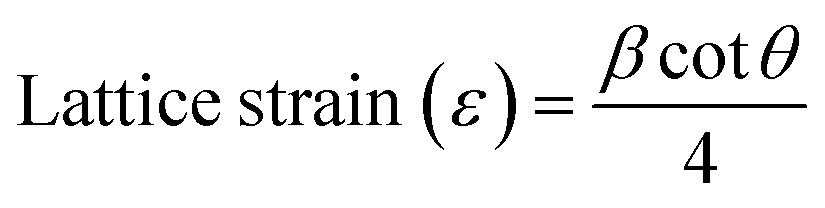
Here, FWHM β is in radians, wavelength of Cu Kα-line (λ = 1.54 Å), Bragg's angle is θ. The increase in the annealing temperature leads to the increment in the crystallinity of the prepared thin films. Lattice strain, also known as crystal lattice strain, is a deformation or distortion in the regular geometric arrangement (lattice) of atoms within a crystalline material. In a perfect crystal lattice, atoms are arranged in a specific and repeating pattern. When a crystal lattice is subjected to external forces, temperature changes, or other factors, it can undergo strain. This can be estimated using the following relation:29| |  | (1b) |
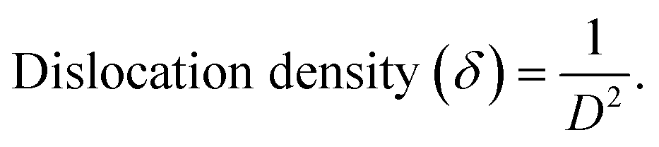
Dislocation density is a measure of the concentration of crystallographic defects known as dislocations within a crystal lattice. Dislocations are linear defects or disruptions in the regular arrangement of atoms in a crystalline material. They can occur due to various factors such as plastic deformation, thermal stresses, or the presence of foreign particles. Dislocation density can also be defined as follows:30| | 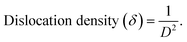 | (1c) |
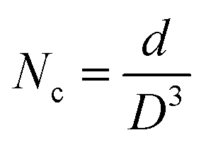
The number of crystallites is contingent upon structural factors such as crystallite dimensions and the extent of clustering or agglomeration. Specifically, the number of crystallites is highly influenced by the size of the crystallites within the material. Hence, the number of crystallites per unit volume (NC) can be estimated by using the ‘D’ value,30| |  | (1d) |
 |
| | Fig. 1 (a) Illustration of XRD patterns, (b) peak shift of (015) and (c) increment in the crystallite sizes of as-grown and annealed Bi2Te3 thin films. | |
Table 1 shows the values of crystallite size as 14.74, 14.97 and 35.51 nm for as-grown and 473 K and 523 K annealed films, respectively. From the estimated values of crystallite size, it is clearly seen that the D value increases monotonically after the annealing process as shown in Fig. 1(c). Lattice strain and dislocation density values reduced with increment in annealing temperature. The reduction in the dislocation density of the material is from 3.12 × 10⁻⁴ to 0.23 × 10⁻⁴ nm−2. The improvement in crystallinity resulting from the annealing process contributes to a decrement in disordered states and, consequently, lowers dislocation density.31 Likewise, the value of Nc demonstrates a decreasing trend during the annealing process. The overall change in structural parameters within the crystal can be attributed to crystallite size refinement and the elimination of dislocations within the films. These changes indicate an enhancement in the overall crystalline quality of the films.32,33
Table 1 Evaluated structural parameters of Bi2Te3 films
| Films |
D (nm) |
(ε) |
Δ (nm−2) (×10−4) |
N
c
|
| Asp |
14.74 |
0.0074 |
3.12 |
0.249 |
| 473 K |
14.97 |
0.0079 |
2.97 |
0.238 |
| 523 K |
35.51 |
0.0030 |
0.23 |
0.178 |
3.2. Raman analysis
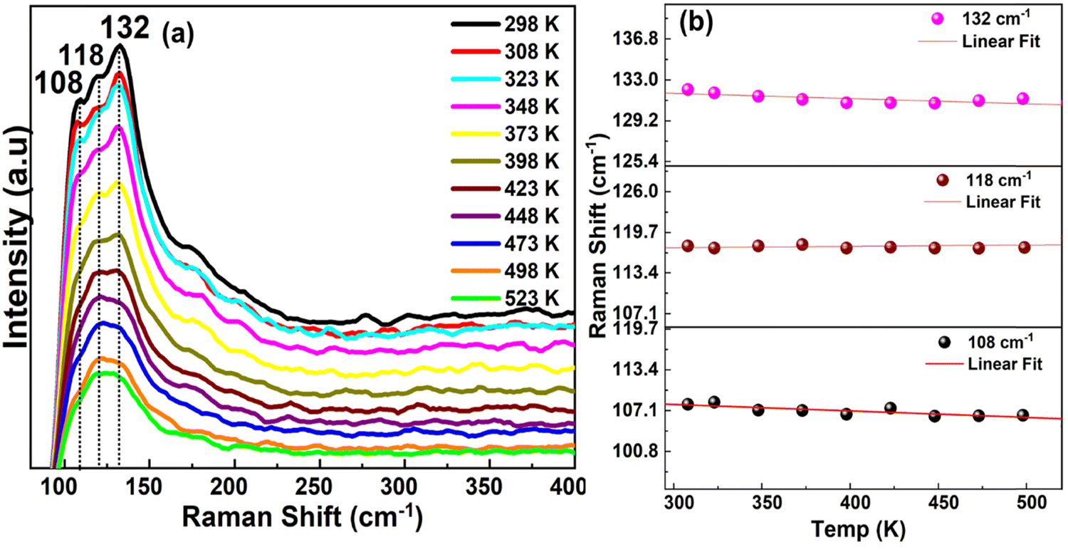
Raman spectroscopy is one of the important characterisation methods, which provides detailed information regarding the microstructural modifications of the material. In the current study, Raman peaks are found at 108 cm−1, 116 cm−1 and 132 cm−1, as presented in Fig. S1 (ESI†). For the as-grown thin film, the Raman spectrum shows only one peak, i.e., at 118 cm−1. However, upon annealing, the Raman spectrum becomes more prominent. For the 473 K annealed film, it exhibits one prominent peak around ∼116 cm−1, which obviously corresponds to the Bi2Te3 vibrational modes.34 Furthermore, for the 523 K annealed one, it shows three peaks: a less intense peak at 108 cm−1 and 118 cm−1 and a prominent peak at 132 cm−1. As the Bi2Te3 thin film is rhombohedral in nature with the R![[3 with combining macron]](https://www.rsc.org/images/entities/char_0033_0304.gif) m space group, it consists of five atoms in its primitive cells. This results in 15 lattice vibrational modes that include 12 optical and 3 acoustic modes at the Brillouin zone.34 The peak around 108 cm−1 corresponds to the vibrational frequencies of the smaller crystallites present in the Bi2Te3 thin films.35 The peaks at 118 and 132 cm−1 correspond to the A1u and A21g modes of Bi2Te3 thin films.36 The peak intensity of the A1g mode is more than those of the other two peaks, indicating symmetric out of plane stretching of Bi–Te atoms.37
m space group, it consists of five atoms in its primitive cells. This results in 15 lattice vibrational modes that include 12 optical and 3 acoustic modes at the Brillouin zone.34 The peak around 108 cm−1 corresponds to the vibrational frequencies of the smaller crystallites present in the Bi2Te3 thin films.35 The peaks at 118 and 132 cm−1 correspond to the A1u and A21g modes of Bi2Te3 thin films.36 The peak intensity of the A1g mode is more than those of the other two peaks, indicating symmetric out of plane stretching of Bi–Te atoms.37
In the current report, we have performed the temperature dependent Raman study of the 523 K annealed Bi2Te3 thin film. Fig. 2(a) shows all the prominent peaks observed for the material. During Raman characterization, the previously annealed film was subjected to annealing over a temperature range varying from 298 K to 523 K. The Raman spectra were recorded at these temperatures for the higher temperature annealed film. With the enhancement of the temperature, the smaller crystallites disappeared, leading to decreased intensity of the peak. Under annealing conditions, the Raman peak shifts towards a lower wavenumber region (red shift). Fig. 2(b) presents the Raman shift of three different modes at different temperatures. It clearly indicates the change in the bond strength of the material. This is due to the thermal expansion occurring in the thin films, which affects the interatomic distances and vibrational frequencies of the lattice modes. Furthermore, the increment in the temperature during Raman measurement leads to a significant change in the phase, mostly creating a new phase due to this structural deformation.38
 |
| | Fig. 2 (a) Temperature dependent Raman spectra of Bi2Te3 thin films and (b) plot between Raman shift and temperature. | |
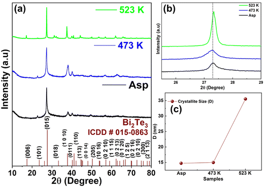
Fig. 3(a)–(c) present the change in FWHM of the corresponding 108, 118 and 132 cm−1 peaks with the temperature, respectively. The increment in the FWHM value with the temperature indicated the peak broadening of the different modes. As the temperature increases, the material tends to expand, leading to a change in the lattice parameters.39 Also, the elevated temperature enhances phonon–phonon interactions, resulting in more complex and broadened spectral features. These interactions also involve harmonic and anharmonic processes.38
 |
| | Fig. 3 Plot of shift in FWHM vs. temperature for (a) 108 cm−1, (b) 118 cm−1 and (c) 132 cm−1 peaks observed for Bi2Te3 thin films. | |
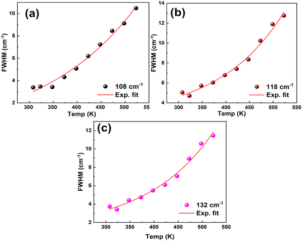
3.3. FESEM and EDX analyses
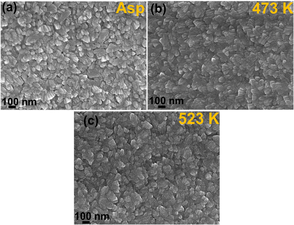
FESEM pictures of the material illustrates the morphology, surface texture and other alterations in the material due to various energy treatments. Fig. 4(a)–(c) show the FESEM pictures of as-grown and annealed Bi2Te3 films. Fig. 4(a) shows the FESEM image of the as-deposited sample. It shows the uniformity in the structure of the material. However, after the annealing process, there is a slight change in the material's surface. Due to the heating process some of the materials form aggregates and this tends to increase the particle size. Again, the increase in the surface area actually enhanced the available area of the material for use as the absorber layer. Meanwhile, the enhanced particle size also results in the reduction of optical bandgap, thus leading to better absorbance. However, the thermal annealing process also influences the surface roughness and porosity of the films. The EDX spectra present the elemental composition of the sample, as shown in Fig. S2 (ESI†). The data were collected from different portions of the films, which show the presence of Bi and Te elements. The peak found around 2.43 keV corresponds to Bi–Mα. The energy spectra showed peaks around 0.65 keV and 3.75 keV, indicating the presence of Te–Lα. For experimental purposes, carbon tape is used for the conduction process, and hence the peak around 0.27 keV indicates the presence of C–Lα. Fig. S3 (ESI†) illustrates the elemental mapping of the 523 K annealed film. It also confirms the distribution of all the constituent elements in the sample. Fig. S3(a)–(c) (ESI†) show the elemental mapping of Bi and Te in the studied films.
 |
| | Fig. 4 FESEM pictures of (a) as-grown and (b) 473 K and (c) 523 K annealed Bi2Te3 films. | |
3.4. TEM analysis
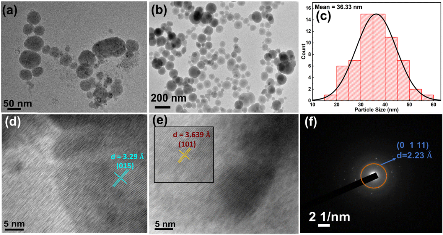
TEM is considered as one of the powerful tools to analyse the exact crystal morphology as well as structural parameters. Fig. 5(a) and (b) illustrate the TEM morphology of the 523 K annealed film. Fig. 5(c) shows the particle size distribution of the material, which is ∼36.33 nm. This is also very close to the crystallite size calculated from the XRD pattern. Fig. 5(d) and (e) present the HRTEM images of the material. Fig. 5(d) shows the presence of the Bi2Te3 (015) plane with the d spacing of 3.29 Å in the sample, whereas Fig. 5(e) confirms the presence of the (101) plane with d = 3.63 Å. Fig. 5(f) shows the SAED pattern, confirming the presence of the rhombohedral Bi2Te3 (015) plane in the material, which is in good agreement with the XRD study.
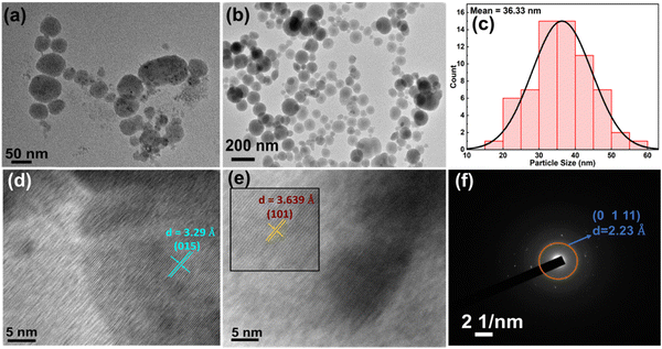 |
| | Fig. 5 (a and b) TEM pictures, (c) particle size distribution plot, (d and e) HRTEM images and (f) SAED pattern of the 523 K annealed Bi2Te3 film. | |
3.5. Optical study
3.5.1. PL analysis.
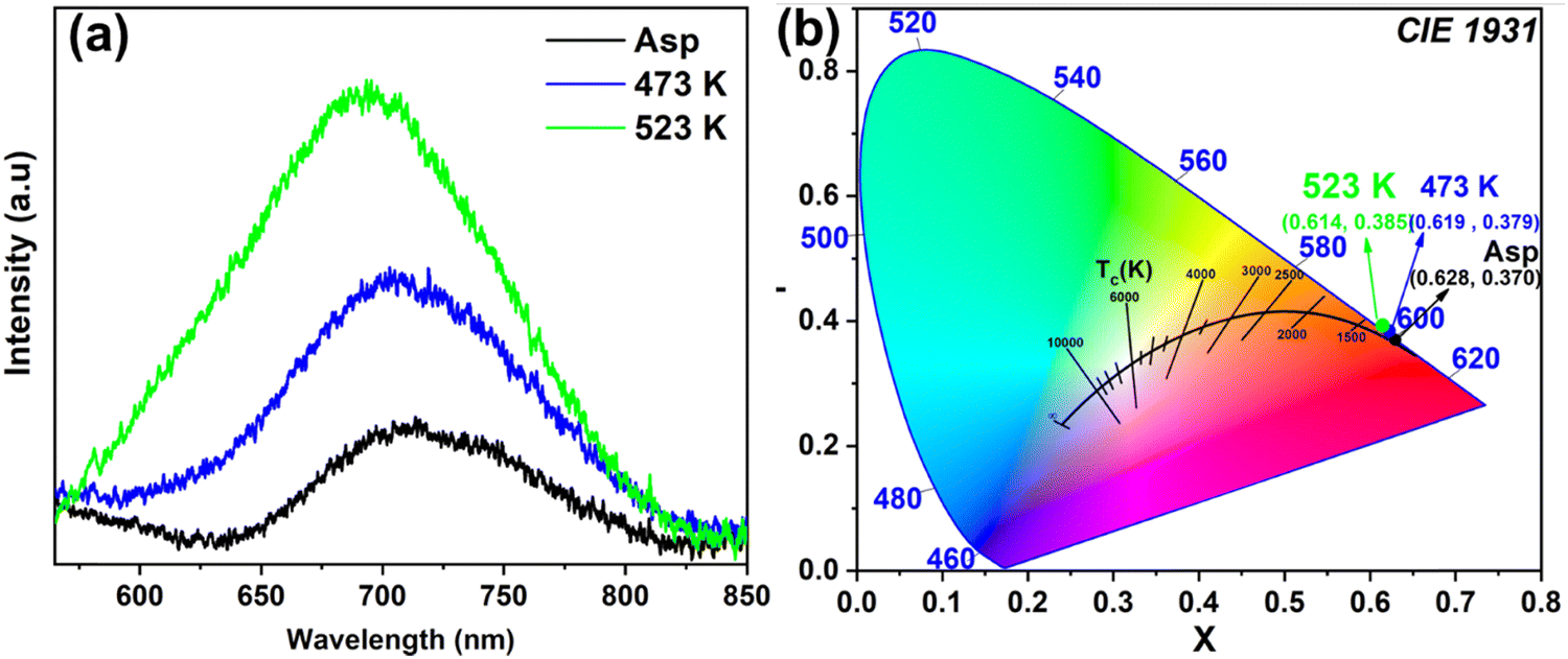
The PL measurements of the as-grown and annealed Bi2Te3 films were performed at 550–850 nm with laser excitation at 532 nm. PL involves the recombination of the electron–hole pairs and leads to the emission of photons. Fig. 6(a) shows the PL spectra of both the films. There is a shift in the PL peak position towards a lower wavelength with annealing, as clearly seen in Fig. 6(a). The peaks found around 712, 704 and 694 nm correspond to as-grown and 473 K and 523 K annealed films, respectively. This blueshift observed in this case may be because of increase in crystallinity and reduction in the defect states. The reduction in the defect-related energy level can shift the PL peaks towards higher energies. Similarly, annealing improves the carrier mobility, which changes the dynamics of electron–hole recombination contributing to a blue shift in the PL spectra.40,41 For various practical application purposes, it is necessary to understand the chromaticity of the material. Fig. 6(b) presents the 1931 Commission Internationale de l’Éclairge (CIE) diagram of the spectra shown in Fig. 6(a). The coordinates of (0.628, 0.370), (0.619, 0.379) and (0.614, 0.385) are observed for as-grown and 473 K and 523 K annealed films, respectively, from the CIE diagram.42
 |
| | Fig. 6 (a) PL spectra and (b) CIE chromaticity coordinates with the CCT scale of as-grown and 473 K and 523 K annealed Bi2Te3 films. | |
In the current case, the emission occurred in greater energy ranges than optical bandgaps. This behaviour occurs mostly due to the following reasons, such as excitonic effects, defects and impurities and other Auger recombinations. Such emission in our case may be due to the smaller crystallites present in the material.40,42
3.5.2. Transmittance (T), absorption coefficient (α) and optical bandgap (Eg).
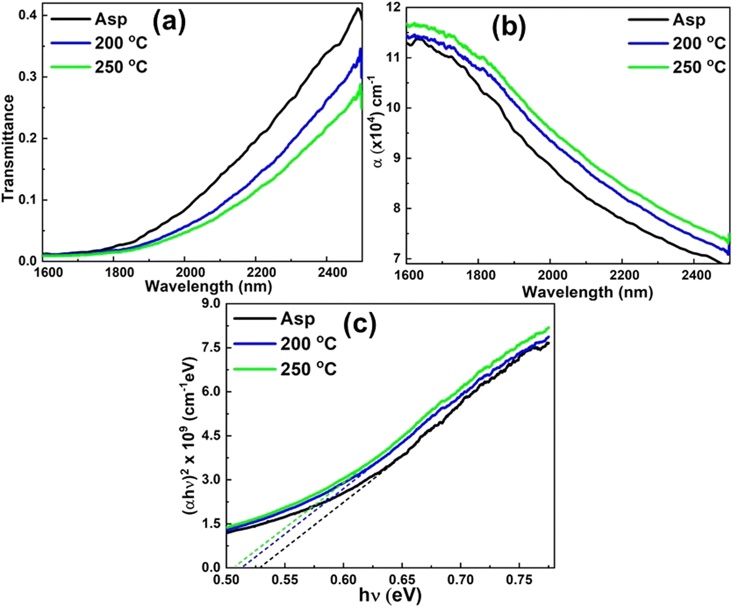
Optical properties are some of the important parameters determining the applicability of the films. Fig. 7(a) shows the change in the transmittance of the as-grown and annealed Bi2Te3 films. There is reduction in transmittance upon thermal annealing over a higher wavelength regime. For this particular case, the transmittance is observed in the infra-red regime, and hence the annealed films can be considered to have possible applications in infra-red related devices. As the annealing temperature increases, the crystallinity shows a pronounced increase, which leads to increased light scattering and a reduced transmittance value.
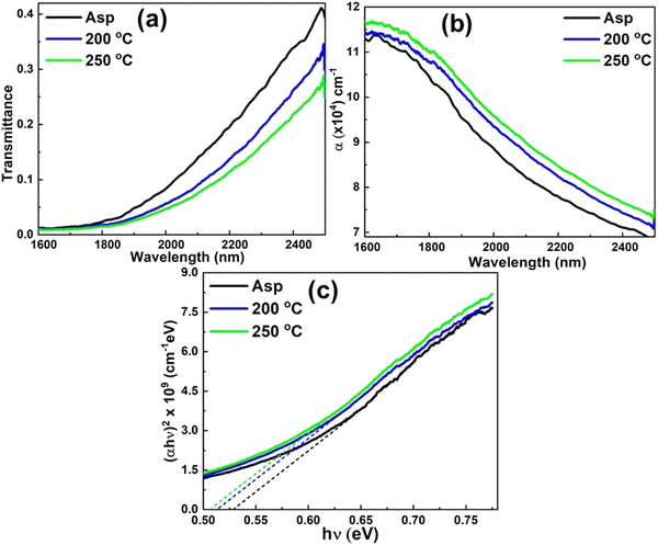 |
| | Fig. 7 (a) Change in transmittance, (b) change in ‘α’ and (c) (αhν)2vs. (hν) plot for bandgap calculation of as-grown and annealed Bi2Te3 films. | |
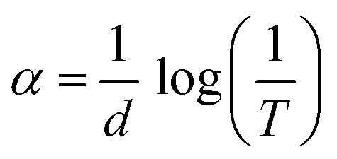
The absorption coefficient (α) of a thin film quantifies its capability to absorb light at a particular wavelength, playing a pivotal role in comprehending the material's optical characteristics. Fig. 7(b) illustrates the absorption coefficient vs. wavelength plot. The ‘α’, which is estimated from the transmittance and thickness of the film, is given by:43
| |  | (2) |
Here, the film thickness is denoted as ‘
d’, which is ∼800 nm. The change in ‘
α’ with ‘
λ’ is shown in
Fig. 7(b). The
α values are of 10
4–10
5 cm
−1 order over the 1600–1800 nm IR range. As the annealing temperature increases, there is an observable shift in the absorption edge towards longer wavelengths. This red shift is primarily attributed to increment in the material's absorption properties. Furthermore, the improvement in crystallinity also contributes to alterations in the optical behaviour.
44
Chalcogenide materials exhibit distinct absorption characteristics, with absorption edges categorized into three main regions: low absorption region (α < 102 cm−1); medium absorption (α ∼ 102–104 cm−1); and high absorption regimes (α > 104 cm−1). The α ≥ 104 cm−1 regime is known as the high absorbance region, where conduction and valence band transitions occur. It is also known as the Tauc region, which generally helps to estimate the bandgap energy, Eg, given by:43
Here the symbols
ν and
h have their usual meaning of frequency and Planck's constant. The exponent ‘
m’ determines the nature of transition occurring in the sample and it is called the transition factor. It also signifies the electron-density profile over valence and conduction bands. It has different values like 1/2 and 3/2 for direct allowed and direct forbidden transitions. The
m = 2 and 3 refer to the indirect allowed and forbidden transition cases. The so-called Tauc parameter is denoted as B whose numerical value represents the degree of disorder in the bandgap regime. The studied material showed high crystalline nature confirmed by the XRD pattern, and so here
m = 1/2 has been considered for the bandgap estimation. The change in (
αhν)
2vs. hν is shown in
Fig. 7(c), where the linear fitting of the data points allowed the estimation of the optical bandgap. The slope determines the Tauc parameter ‘B’ and the intercept on the
X-axis measures the ‘
Eg’ value. The estimated
Eg and
B2 values for both the films are presented in
Table 2. The direct bandgap of the material exhibits a decreasing trend, measuring 0.528 eV for the as-prepared sample, 0.510 eV for the 473 K annealed thin film, and 0.506 eV for the 523 K annealed film. The Tauc parameter values are 3.23 × 10
10 cm
−2 eV
2, 3.19 × 10
10 cm
−2 eV
2 and 3.10 × 10
10 cm
−2 eV
2 for as-prepared and 473 K and 523 K annealed thin films, respectively. The Mott and Davis “density of state model” states that the annealing process enhances the crystallization of the material.
45 This results in an increment in the number of dangling bonds around the surface of the crystallites, leading to a higher concentration of localized states. The widening of these localized states contributes to a reduction in the bandgap. The alterations in the bandgap are notably impacted by surface morphology, specifically influenced by varying annealing temperatures.
46
Table 2 Estimated optical parameters of as-grown and annealed Bi2Te3 films
| Optical parameters |
As-prepared film |
473 K annealed film |
523 K annealed film |
| Optical bandgap (Eg), eV |
0.528 |
0.510 |
0.506 |
|
B
2 × 1010 cm−2 eV2 |
3.23 |
3.19 |
3.10 |
|
E
u (eV) |
0.394 |
0.440 |
0.456 |
| Steepness parameter (σ) × 10−3 |
65.22 |
58.40 |
56.35 |
| (Ee–p) × 10−3 |
10.22 |
11.41 |
11.83 |
| NEAR |
0.978 |
0.980 |
0.982 |
| Static refractive index (n0) |
4.05 |
4.09 |
4.10 |
| High frequency dielectric constant ε∞ |
16.46 |
16.78 |
16.86 |
|
n
2 × 10⁻⁹ esu |
3.62 |
3.90 |
3.96 |
|
χ
(1) in esu |
1.23 |
1.25 |
1.26 |
|
χ
(3) × 10−10 esu |
3.90 |
4.24 |
4.32 |
| Optical electronegativity (ηopt) |
1.583 |
1.580 |
1.579 |
In examining the low absorption regime of the material, the Urbach rule is predominantly employed to investigate its nature. This is because, in this region, the absorption coefficient follows an exponential change with photon energy (hν). The Urbach energies (Eu) of the as-grown and annealed thin films are obtained using the relation:47
| |  | (4) |
where
α0 is a constant factor. The
Eu value provides valuable insights into the level of disorder within the material. It serves as an indicator of band tail width associated with localized states within the gap region.
Eqn (4) shows that the
Eu can be computed by taking the inverse of the slope. The transition between one band's extended states and the other bands' exponential tails primarily occurs in this lower absorption region.
Table 2 tabulates the expected values of
Eu. The
Eu value shows an increasing trend from 0.394 to 0.456 eV. The electron–phonon interaction (E
e–p) and steepness of absorption edge (
σ) are two essential features that only provide information about the structural behavior of the material at the absorption edge. The two parameters are determined as follows:
48| | | σ = kBT/Eu and Ee–p = 2/3σ | (5) |
where
kB is the Boltzmann constant and
T is the absolute temperature. The
σ values of as-grown and annealed films are 65.22 × 10
−3, 58.40 × 10
−3 and 56.35 × 10
−3, respectively. The calculated values are presented in
Table 2. By increase annealing temperature,
σ values reduce with increased crystallinity of films. The estimated values of
Ee–p are 10.22 × 10
−3, 11.41 × 10
−3 and 11.83 × 10
−3 for as-grown and 473 K and 523 K annealed films, respectively (
Table 2). This also explains why the ionicity and anion valence of thin film samples changed.
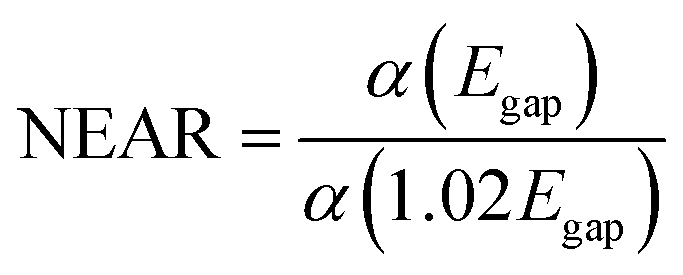
Urbach tails are caused by defects in the chalcogenide material and are close to the band-edge. The near edge absorptivity ratio (NEAR) in the Tauc region determines the Urbach tail's magnitude. The NEAR is defined as:49
| |  | (6) |
The NEAR values vary from 0.978 to 0.982 (
Table 2), which indicates the change in the defect states in the film structure.
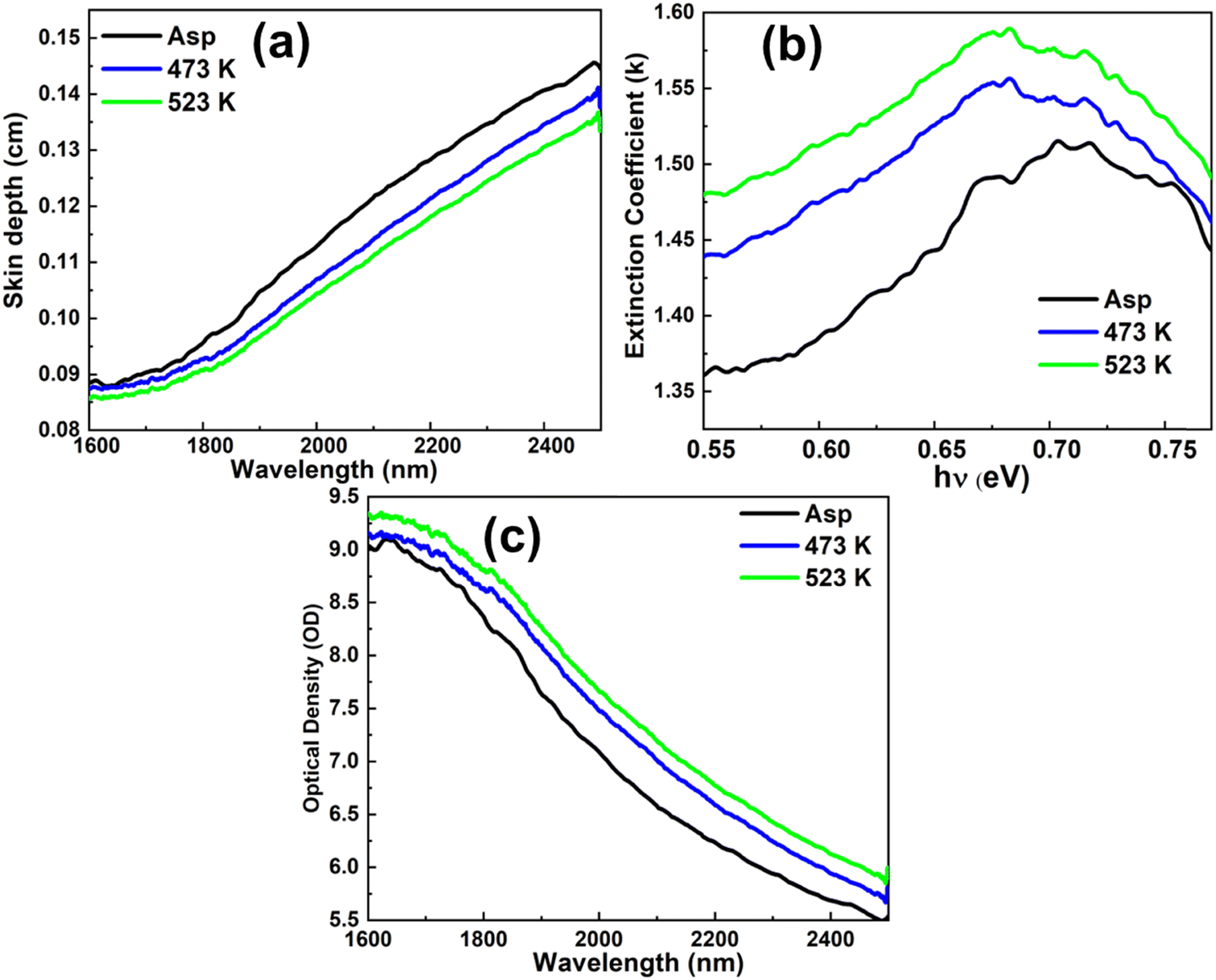
3.5.3. Skin depth (δ), extinction coefficient (k) and optical density (OD).
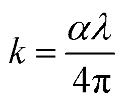
The skin depth (δ) is the path distance at which the incident radiation intensity is reduced to the 1/e value during its movement inside the sample. It is calculated as 1/α, i.e. the reciprocal of α.50 The change in ‘δ’ as a function of energy is presented in Fig. 8(a), which shows the reduction of δ with hν. Different multimode optical fiber applications are made possible for such decreased δ values at a specific wavelength. The extinction coefficient (k) characterizes the energy loss experienced as electromagnetic waves propagate within a material, also recognized as the loss factor. The value of ‘k’ is determined according to ref. 51,  . The relationship between ‘k’ and hν reveals an escalating trend in the k value, which is shown in Fig. 8(b). The change in ‘k’ also tends to affect the nonlinearity of the material. Similarly, the material's optical density (OD) is related to the absorption ability of the material during its exposure to electromagnetic radiation. It is estimated as the product of absorption coefficient and film thickness,52i.e., OD = α × t. Fig. 8(c) presents the OD variation with λ, which changes like α. Following annealing, the OD values exhibit an increased trend, reaching saturation in the higher wavelength region.
 |
| | Fig. 8 Variation of (a) skin depth, (b) extinction coefficient and (c) optical density for as-grown and annealed Bi2Te3 films. | |
3.5.4. Linear static refractive index (n0) and high-frequency dielectric constant (ε∞).
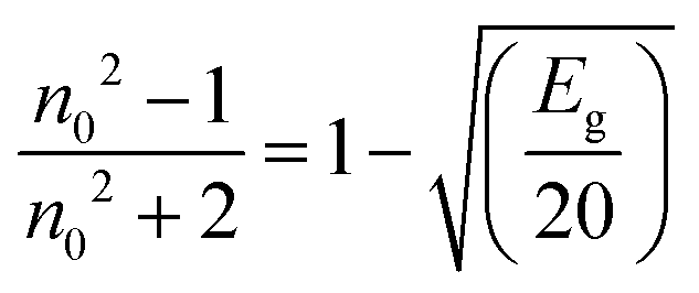
The refractive index (n) at hν → 0, named the static refractive index (no), can be estimated for all synthesized samples from the Dimitrov and Sakka empirical formula,53| |  | (7) |
The estimated values of n0 for all samples by considering bandgap values are given in Table 2. The values of n0 are 4.05, 4.09 and 4.10 for as-grown and 473 K and 523 K annealed films, respectively. According to Moss's rule, the refractive index is inversely proportional to the optical bandgap value, i.e., Egn4 ∼ constant.54 The high-frequency dielectric constant, ε∞ = no2, shows the values of 16.46, 16.78 and 16.86 for as-grown and 473 K and 523 K annealed films, respectively, which are tabulated in Table 2.
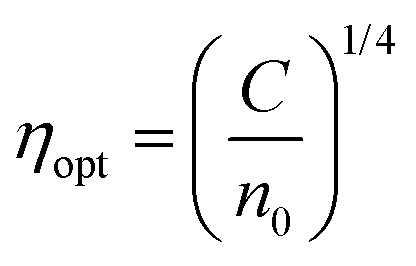
The electronegativity (ηopt) of the as-grown and annealed bilayer films has been estimated as,55 with ‘C’ as a constant (C = 25.54). It defines the attraction ability of the positive radicals to the electrons to form ionic bonds. The electronegativity values are 1.583, 1.580 and 1.579 for as-grown and 473 K and 523 K annealed films, respectively (Table 2).
3.5.6. Nonlinear optical parameters.
3.5.6.1. First-order nonlinear susceptibility (χ(1)), third-order nonlinear susceptibility (χ(3)) and non-linear refractive index (n2).
Chalcogen-based films are particularly promising for a range of nonlinear optical applications due to their distinctive characteristics, including higher nonlinearity and a significant interaction domain. Unlike linear behaviour, the polarization of these films responds to an applied electric field in a nonlinear manner, further enhancing their suitability for diverse applications in nonlinear optics. The exposure of the sample to intense electromagnetic radiation/light results in the nonlinear phenomena in the sample. The linear polarization is lost in the case of high intensity radiation interaction of the sample and in this case, polarization varies with multi-power of electric field. In a linear system, the response is directly proportional to the applied stimulus (e.g., an electric field), following a linear relationship, P = ε0χE. However, in the case of chalcogenide materials, the relationship becomes nonlinear under certain conditions. This modifies the induced polarization (P) vector by series expansion in terms of applied electric field (E) and susceptibility (χ) as follows:59| | | P = ε0[χ(1)·E + χ(2)·E2 + χ(3)·E3 + …] | (8) |
with linear polarization being ‘χ(1)’ and the remaining part contributing to the nonlinear response. However, for centrosymmetric media, the 2nd order nonlinear susceptibility becomes zero due to the absence of inversion symmetry. So, the major contribution towards nonlinear phenomena is governed by the 3rd order nonlinear susceptibility (χ(3)) in many semiconducting materials. The values of both χ(1) and (χ(3)) are calculated as:60,61| |  | (9) |
with ‘A’ being a constant factor of ∼1.7 × 10⁻¹⁰ and not the static refractive index. The χ(1) value varies from 1.23 to 1.26 esu and χ(3) varies from 3.90 × 10⁻¹⁰ esu to 4.32 × 10⁻¹⁰ esu, for as-grown and annealed thin films (Table 2). Such tuning of χ(3) values is useful for fiber fabrication and optical communication purposes. The change in χ(3) with bandgap under annealing conditions is shown in Fig. S4(b) (ESI†).
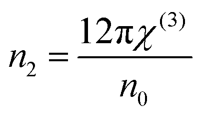
The quantity Δn (change in the refractive index) originates from the nonlinear response as given by Δn = n2|E|2, where ‘n2’ is the nonlinear refractive index and ‘E’ is the applied electric field. The n2 values of the as-grown and annealed films were determined using Ticha–Tichy and Miller's formula as:61 and are given in Table 2. The values are 3.62 × 10⁻¹⁰ esu, 3.90 × 10⁻¹⁰ esu and 3.96 × 10⁻¹⁰ esu for as-grown and 473 K and 523 K annealed films, respectively. The increased n2 value upon annealing is suitable for nonlinear device fabrication. The existence of significant nonlinearities presents an opportunity to develop compact and energy-efficient devices for telecommunications. The feasibility of creating small, low-power telecommunications devices is enhanced, as larger nonlinearity requires less energy and results in shorter interaction lengths.62,63
3.6. Surface wettability study
Adhesion related to wetting is a crucial element and a widely employed technique for assessing the surface characteristics of materials, which is often accomplished through contact angle measurement. The assessment of wetness of the surfaces involves studying the solid and liquid interaction, and this process is termed contact angle measurement. The microscopic parameter defining a material's wettability is known as the contact angle (θ). For high wettability, the contact angle (θ) is small, indicating the hydrophilic nature of the material Conversely, the contact angle (θ) is high for low wettability, indicating the hydrophobic nature of the material's surface. This measurement provides valuable insights into the affinity of a material for liquids, facilitating a nuanced understanding of its surface properties.64
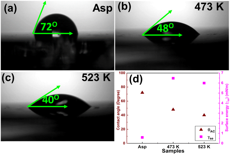
Fig. 9(a)–(c) present the contact angle measurement of as-grown and annealed Bi2Te3 samples. The as-prepared sample shows a contact angle of around 72°, which indicates its hydrophilic nature. 473 K and 523 K annealed films show 48° and 40° contact angles, respectively. There is gradual enhancement in the hydrophilic nature of the films with annealing temperature. The surface free energies (γ) of these as-grown and annealed films were calculated using the relation:65 with γw = 71.99 mN m−1 (surface tension of water). The calculated values of γse are 0.58, 6.47 and 5.99 for as-grown and 473 K and 523 K annealed films. The thermal induced hydrophilicity of the material mostly increased due to the surface structure, change in the surface roughness and sometimes due to the oxygen vacancy sites. In the current case, the surface structure and surface roughness seemed to remain the same for annealed films, which shows the healing of atomic impairment. Fig. 9(d) shows a comparative plot between the contact angle and surface energy of the as-grown and annealed thin films.66
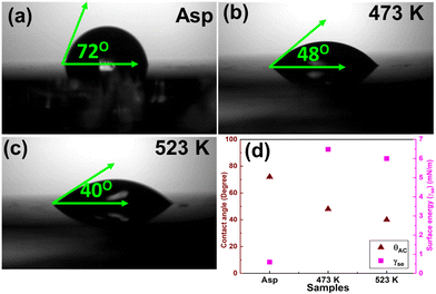 |
| | Fig. 9 Contact angle measurement of (a) as-prepared and (b) 473 Kand (c) 523 K annealed films and (d) comparative plot between contact angle and surface energy of the as-grown and annealed Bi2Te3 samples. | |
3.7. Photo-response study
Group V–VI Bi2Te3 thin films are mostly considered as semiconducting materials.67 The performance of the Bi2Te3 thin films as photodetectors is greatly affected by the photo-response properties of the materials. Firstly, the current versus voltage measurement (I–V characteristics) was performed for both as-prepared and annealed films. Fig. 10(a)–(c) illustrate the I–V plot of as-prepared and 473 K and 523 K annealed Bi2Te3 thin films under dark and illumination conditions, respectively. For illumination, the prepared material was illuminated under 20, 40 and 60 mW powers of 532 nm green laser. With the increment in the laser power of the material, there is a gradual increment in the current value for all the materials. With the enhancement of the annealing temperature, the annealed Bi2Te3 thin films exhibit good photo-conductivity compared to the as-prepared one. The resistances of the as-prepared and annealed Bi2Te3 samples are shown in Fig. S5 (ESI†). The figure clearly shows the reducing trend of the resistance value, which also indicates the increment in the conductivity of the material. The I–V measurement of the material clearly shows a linear plot, with the current in the mA range.
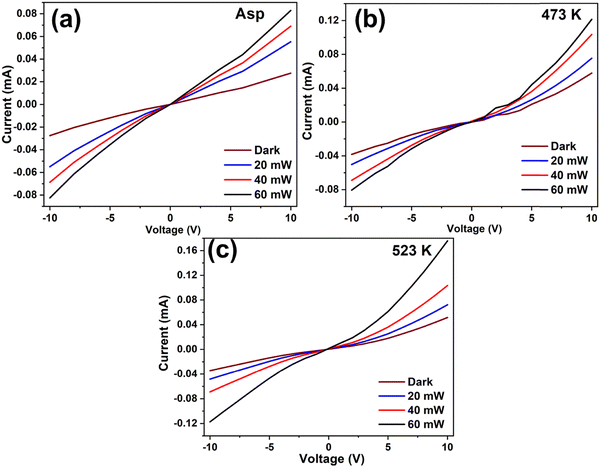 |
| | Fig. 10
I–V characteristics of as-prepared and 473 K and 523 K annealed Bi2Te3 thin films under OFF (dark) and ON illumination conditions. | |
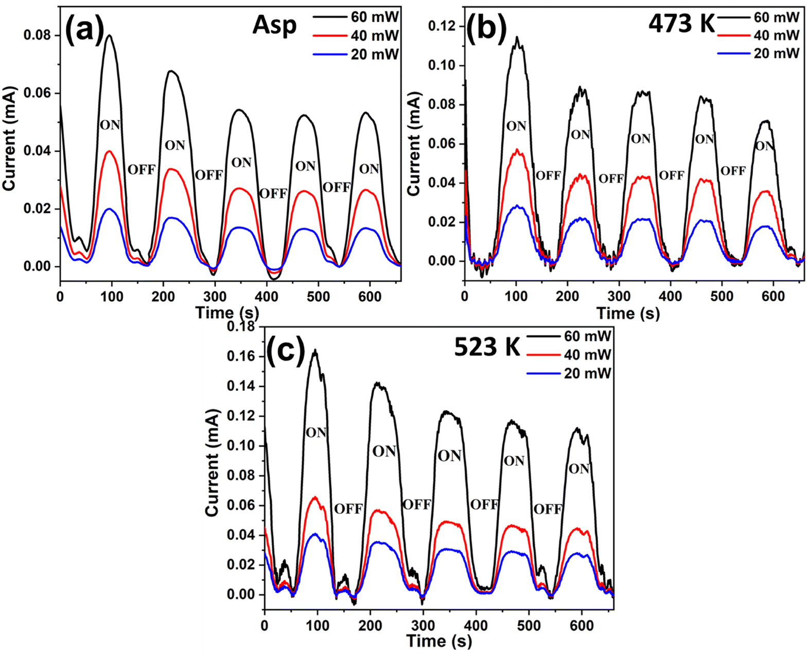
For further investigation of the photo-response properties of the material, it is illuminated under the green laser. With the variation in the laser power from 20 to 40 to 60 mW, the active region of the sample gets illuminated. Fig. 11(a)–(c) present the clear photo-switching behaviour of the as-prepared and annealed thin films upon switching ON/OFF the laser illumination. The measurement is taken at a 60 second time interval. The current of the material gradually increased with the enhancement of the laser power. The photo-response mechanisms of both as-prepared and annealed Bi2Te3 thin films follow quite similar procedures to those of bismuthine and tellurene.68 This response occurred due to (i) formation of an electron–hole pair upon photoexcitation and (ii) photoinduced charge transportation. Here, the photocurrent exhibits a positive dependence on the incident power, which is attributed to the enhancement of the number of photogenerated carriers.69,70 Several parameters, including responsivity (R), detectivity (D) and external quantum efficiency (EQE), can be used to verify the device performances.
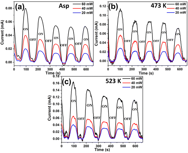 |
| | Fig. 11 Time dependent photocurrent under different illumination conditions of (a) as-prepared and (b) 473 K and (c) 523 K annealed Bi2Te3 thin films. | |
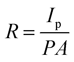
Responsivity is defined as the photocurrent generated by the excitation of unit incident power. It can be estimated using the relation:
| |  | (10) |
where
Ip is the photocurrent,
P is the power density and
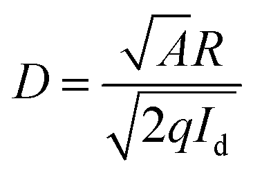
A is the active area. Detectivity refers to the ability of the material to detect the weak optical signal. It can be evaluated according to the equation:
| |  | (11) |
where
Id is the dark current. For the as-prepared Bi
2Te
3 thin film sample, the
R and
D values are 40 A W
−1 and 8 × 10
9 Jones under 60 mW power of 532 nm laser irradiation. Similarly, for 473 K and 523 K annealed films, the
R values are 80 A W
−1 and 100 A W
−1, respectively, under 60 mW laser illumination. On the other hand, the
D values are 9.12 × 10
10 Jones and 9.88 × 10
10 Jones, respectively. In comparative Table S1 (ESI
†), all the related figure of merits of Bi
2Te
3 based photodetectors are given. Other important factors for investigating the photodetector are response time (
tres) and recovery time (
trec). Here, the response time (
tres) and recovery time (
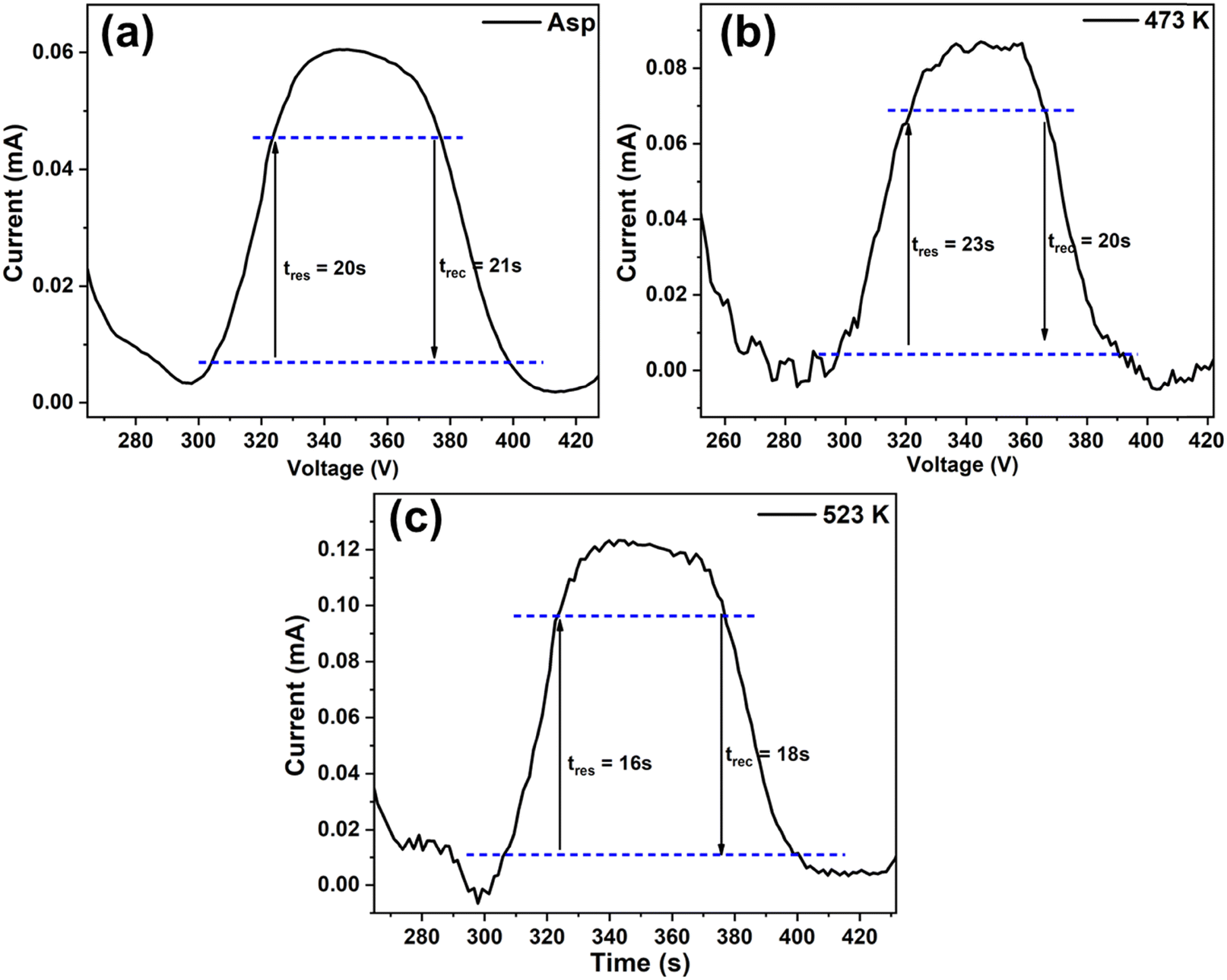
trec) were ascribed to the time interval for the rise and decay from 10% to 90% and from 90% to 10% of the peak value of the current, respectively.
Fig. 12 illustrates the response and recovery time plots of as-prepared and other annealed Bi
2Te
3 films. From these plots, it can be concluded that for the as-prepared one,
tres and
trec are 20 s and 21 s, respectively. Similarly, from
Fig. 12(b), the
tres and
trec are 23 s and 20 s for the 473 K annealed one. Lastly,
Fig. 12(c) presents the lowest
tres and
trec of 16 s and 18 s for the 523 K annealed one, respectively.
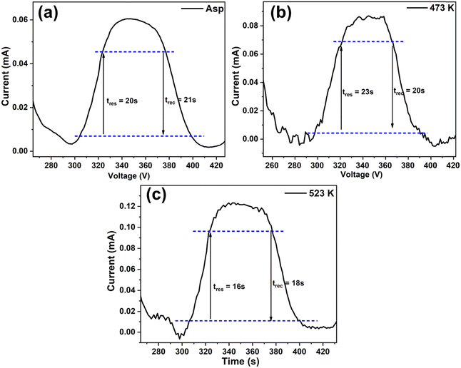 |
| | Fig. 12 The tres and trec of (a) as-prepared, (b) 473 K and (c) 523 K annealed Bi2Te3 thin films at 60 mW laser power. | |
4. Conclusion
In the current report, the annealing induced modifications in the as-grown and annealed Bi2Te3 films were studied thoroughly by different characterization methods. The XRD study confirmed the presence of rhombohedral phase and the increment in the crystallinity due to thermal annealing. The temperature dependent Raman study showed a red shift in the vibrational modes of the material. This clearly shows the enhanced thermal conductivity of the material, due to the increment in the phonon–phonon interactions. The FESEM images show increment in the surface porosity and agglomeration of the material. The TEM study confirmed the different crystal planes and the average particle size of ∼36 nm for the 523 K annealed sample. The PL spectra confirm a blue shift in the emission peak, and the chromaticity diagram also confirms the shift in the colour coordinates. The optical study showed the reduction in the transmittance value and good optical properties in the infra-red region with the increase in annealing temperature. The absorption edge shows a red shift leading to decrease in the optical bandgap from 0.528 to 0.506 eV. The non-linear susceptibility and refractive index were enhanced by annealing treatment, as required for nonlinear optical devices. The surface wettability of the thin film shows higher hydrophilicity with the increase in the annealing temperature. The photo-response study of the material shows increased photo-current compared to that observed under dark conditions. With the illumination of green laser, the photo-response study revealed the possibility of using the material as a photodetector device. All these key results made the material suitable for infra-red related devices and non-linear optoelectronic applications.
Data availability
The data that support the findings of this study are available from the corresponding author upon reasonable request.
Conflicts of interest
There are no conflicts of interest for this manuscript.
Acknowledgements
The author Dr R. Naik thanks the Central Instrumentation Facility of ICT-IOC for different characterizations.
References
- R. Woods-Robinson, Y. Han, H. Zhang, T. Ablekim, I. Khan, K. A. Persson and A. Zakutayev, Wide band gap chalcogenide semiconductors, Chem. Rev., 2020, 120, 4007–4055 CrossRef CAS PubMed.
- B. Saparov, Next generation thin-film solar absorbers based on chalcogenides, Chem. Rev., 2022, 122, 10575–10577 CrossRef CAS PubMed.
- C. Lu, M. Luo, W. Dong, Y. Ge, T. Han, Y. Liu, X. Xue, N. Ma, Y. Huang, Y. Zhou and X. Xu, Bi2Te3/Bi2Se3/Bi2S3 cascade heterostructure for fast-response and high-photoresponsivity photodetector and high-efficiency water splitting with a small bias voltage, Adv. Sci., 2023, 10, 2205460 CrossRef CAS PubMed.
- S. Aminorroaya Yamini, R. Santos, R. Fortulan, A. A. Gazder, A. Malhotra, D. Vashaee, I. Serhiienko and T. Mori, Room-temperature thermoelectric performance of n-type multiphase pseudobinary Bi2Te3–Bi2S3 compounds: synergic effects of phonon scattering and energy filtering, ACS Appl. Mater. Interfaces, 2023, 15, 19220–19229 CrossRef CAS PubMed.
- Y. X. Zhang, Y. K. Zhu, D. S. Song, J. Feng and Z. H. Ge, Excellent thermoelectric performance achieved in Bi2Te3/Bi23@Bi nanocomposites, Chem. Commun., 2021, 57, 2555–2558 RSC.
- J. Pei, B. Cai, H. L. Zhuang and J. F. Li, Bi2Te3-based applied thermoelectric materials: research advances and new challenges, Natl. Sci., 2020, 7, 1856–1858 Search PubMed.
- A. M. Adam, A. K. Diab, M. Tolan, Z. M. H. El-Qahtani, A. A. Refaat, M. A. El-Hadek, E. M. Elsehly, A. El-Khouly, A. N. Alharbi, V. Khovaylo and M. Ataalla, Outstanding optical properties of thermally grown (Bi2Se3)1-x (Bi2Te3)x thin films, Mater. Sci. Semicond., 2022, 143, 106557 CrossRef CAS.
- J. Fu, J. Huang and F. Bernard, Electronic structure, elastic and optical properties of Bi2Te3/Sb2Te3 thermoelectric composites in the periodic-superlattice thin films, Compos. Commun., 2021, 28, 100917 CrossRef.
- K. Rani, V. Gupta, Ranjeet and A. Pandey, Improved thermoelectric performance of Se-doped n-type nanostructured Bi2Te3, J. Mater. Sci.: Mater. Electron., 2023, 34, 1074 CrossRef CAS.
- X. Li, C. Lou, X. Li, Y. Zhang, Z. Liu and B. Yin, Bi2Te3/Sb2Te3 thermophotovoltaic cells for low temperature infrared radiation, J. Phys. D: Appl. Phys., 2019, 53, 035102 CrossRef.
- S. Das, S. Senapati, D. Alagarasan, S. Varadharajaperumal, R. Ganesan and R. Naik, Thermal annealing-induced transformation of structural, morphological, linear, and nonlinear optical parameters of quaternary As20Ag10Te10Se60 thin films for optical applications, ACS Appl. Opt. Mater., 2022, 1, 17–31 CrossRef.
- S. Das, S. Senapati, D. Alagarasan, R. Ganesan and R. Naik, Laser-induced modification in structural, morphological, linear and non-linear optical parameters of Ge20Ag10Te10Se60 thin films for optoelectronic applications, Mater. Sci. Semicond. Process., 2023, 160, 107456 CrossRef CAS.
- S. Das, S. Senapati, D. Alagarasan, R. Ganesan, S. Varadharajaperumal and R. Naik, Modifications in the structural, morphological, optical properties of Ag45Se40Te15 thin films by proton ion irradiation for optoelectronics and nonlinear applications, Ceram. Int., 2023, 49, 10319–10331 CrossRef CAS.
- S. Vadakkedath Gopi, N. Spalatu, M. Basnayaka, R. Krautmann, A. Katerski, R. Josepson, R. Grzibovskis, A. Vembris, M. Krunks and I. O. Acik, Post deposition annealing effect on properties of CdS films and its impact on CdS/Sb2Se3 solar
cells performance, Front. Energy Res., 2023, 11, 1162576 CrossRef.
- J. Gubicza, Annealing-induced hardening in ultrafine-grained and nanocrystalline materials, Adv. Eng. Mater., 2020, 22, 1900507 CrossRef CAS.
- S. Giri, P. Priyadarshini, D. Alagarasan, R. Ganesan and R. Naik, Annealing-induced phase transformation in In10Se70Te20 thin films and its structural, optical and morphological changes for optoelectronic applications, RSC Adv., 2023, 13, 24955–24972 RSC.
- A. A. El-Saady, A. A. M. Farag, D. M. Abdel Basset, N. Roushdy and M. M. El-Nahass, Tailoring the optoelectronic properties of nanocrystalline β-H2Pc films via thermal annealing: Structural, morphological, and optical analyses, Phys. B, 2023, 669, 415339 CrossRef CAS.
- Z.-H. Zheng, D. Yang, P.-C. Zhang, F. Li, Y.-X. Chen, G.-X. Liang and P. Fan, Enhancement of the thermoelectric properties of Bi2Te3 nanocrystal thin films by rapid annealing, Mater. Lett., 2020, 275, 128143 CrossRef CAS.
- O. Norimasa, T. Chiba, M. Hase, T. Komori and M. Takashiri, Improvement of thermoelectric properties of flexible Bi2Te3 thin films in bent states during sputtering deposition and post-thermal annealing, J. Alloys Compd., 2022, 898, 162889 CrossRef CAS.
- Q.-X. Guo, Z.-X. Ren, Y.-Y. Huang, Z.-C. Zheng, X.-M. Wang, W. Hei, Z.-D. Zhu and J. Teng, Effects of post-annealing on crystalline and transport properties of Bi2Te3 thin films, Chin. Phys. B, 2021, 30, 067307 CrossRef CAS.
- Z. He, Y.-X. Chen, Z. Zheng, F. Li, G. Liang, J. Luo and P. Fan, Enhancement of thermoelectric performance of N-type Bi2Te3 based thin films via in situ annealing during magnetron sputtering, Ceram. Int., 2020, 46, 13365–13371 CrossRef CAS.
- M. Naumochkin, G.-H. Park, K. Nielsch and H. Reith, Study of the Annealing effects of sputtered Bi2Te3 thin films with full thermoelectric figure of merit characterization, Phys. Status Solidi RRL, 2021, 16, 2100533 CrossRef.
- L. Fan, J. Tang, L. Wu, S. Zhang, F. Liu, J. Yao and L. Guo, Rapid growth of high-performance Bi2Te3 thin films by laser annealing at room temperature, Appl. Surf. Sci., 2023, 639, 58164 CrossRef.
- R. Eguchi, H. Yamamuro and M. Takashiri, Enhanced thermoelectric properties of electrodeposited Bi2Te3 thin films using TiN diffusion barrier layer on a stainless-steel substrate and thermal annealing, Thin Solid Films, 2020, 714, 138356 CrossRef CAS.
- C. Sudarshan, S. Jayakumar, K. Vaideki and C. Sudakar, Te-rich Bi2Te3 thin films by electron−beam deposition: Structural, electrical, optical and thermoelectric properties, Thin Solid Films, 2020, 713, 138355 CrossRef CAS.
- A. M. Adam, M. Tolan, A. A. Refaat, A. Nafady, P. Petkov and M. Ataalla, Optical properties of thin Bi2Te3 films synthesized by different techniques, Superlattices Microstruct., 2021, 155, 106909 CrossRef CAS.
- S. R. Jian, P. H. Le, C.-W. Luo and J.-Y. Juang, Nanomechanical and wettability properties of Bi2Te3 thin films: Effects of post-annealing, J. Appl. Phys., 2017, 121, 175302 CrossRef.
- G. Malik, S. Mourya, J. Jaiswal and R. Chandra, Effect of annealing parameters on optoelectronic properties of highly ordered ZnO thin films, Mater. Sci. Semicond., 2019, 100, 200–213 CrossRef CAS.
- O. Norimasa and M. Takashiri, In-and cross-plane thermoelectric properties of oriented Bi2Te3 thin films electrodeposited on an insulating substrate for thermoelectric applications, J. Alloys Compd., 2022, 899, 163317 CrossRef CAS.
- H. P. Cheng, P. H. Le, L. T. C. Tuyen, S. R. Jian, Y. C. Chung, I. J. Teng, C. M. Lin and J. Y. Juang, Effects of substrate temperature
on nanomechanical properties of pulsed laser deposited Bi2Te3 films, Coat, 2022, 12, 871 CrossRef CAS.
- L. Mulder, H. van de Glind, A. Brinkman and O. Concepcion, Enhancement of the surface morphology of (Bi0.4Sb0.6)2Te3 thin films by in situ thermal annealing, Nanomaterials, 2023, 13, 763 CrossRef CAS PubMed.
- S. Das, P. Priyadarshini, D. Alagarasan, S. Varadharajaperumal, R. Ganesan and R. Naik, Structural, morphological, and linear/non-linear optical properties tuning in Ag60-x Se40Tex films by thermal annealing for optoelectronics, J. Non-Cryst. Solids, 2022, 592, 121742 CrossRef CAS.
- M. Sajid, N. Ali, A. Hussain, S. Attique, S. Rauf, A. Javid and N. Dar, Optimizing antimony trisulfide thin films: enhanced structural and optoelectronic properties via post-annealing in sulfur atmosphere, Thin Solid Films, 2023, 782, 140027 CrossRef CAS.
- R. Nepal, V. Sharma, L. Pogue, N. Drichko and R. C. Budhani, Disorder driven variations in magnetoresistance and planar hall effect in Bi2Te3 thin films, Thin Soild Films, 2022, 761, 139520 CrossRef CAS.
- Y. S. Wudil, M. A. Gondal, S. G. Rao, S. Kunwar and A. Q. Alsayoud, Substrate temperature-dependent thermoelectric figure of merit of nanocrystalline Bi2Te3 and Bi2Te2.7Se0.3 prepared using pulsed laser deposition supported by DFT study, Ceram. Int., 2020, 46, 24162–24172 CrossRef CAS.
- S. Buchenau, S. Scheitz, A. Sethi, J. E. Slimak, T. E. Glier, P. K. Das, T. Dankwort, L. Akinsinde, L. Kienle, A. Rusydi and C. Ulrich, Temperature and magnetic field dependent Raman study of electron-phonon interactions in thin films of Bi2Se3 and Bi2Te3 nanoflakes, Phys. Rev. B, 2020, 101, 245431 CrossRef CAS.
- Y. R. Guo, C. Qiao, J. J. Wang, H. Shen, S. Y. Wang, Y. X. Zheng, R. J. Zhang, L. Y. Chen, W.-S. Su and C. Z. Wang, Temperature dependence of structural, dynamical, and electronic properties of amorphous Bi2Te3: an ab initio study, New J. Phys., 2019, 21, 093062 CrossRef CAS.
- B. Huang, G. Li, B. Duan, P. Zhai and W. A. Goddard III, Temperature-dependent anharmonic effects on shear deformability of Bi2Te3 semiconductor, Scr. Mater., 2021, 202, 114016 CrossRef CAS.
- M. Tiadi, D. K. Satapathy and M. Battabyal, Evolution of optical phonon modes and thermoelectric properties in doped Bi2Te3: A temperature-dependent Raman spectroscopy study, Phys. Rev. Mater., 2023, 7, 015401 CrossRef CAS.
- N. Hussain, Q. Zhang, J. Lang, R. Zhang, M. Muhammad, K. Huang, T. Cosseron De Villenoisy, H. Ya, A. Karim and H. Wu, Ultrahigh room-temperature photoluminescence from few to single quintuple layer Bi2Te3 nanosheets, Adv. Opt. Mater., 2018, 6, 1701322 CrossRef.
- B. K. Gupta, R. Sultana, S. Singh, V. Singh, G. Awana, A. Gupta, B. Singh, A. K. Srivastava, O. N. Srivastava, S. Auluck and V. P. S. Awana, Unexplored photoluminescence from bulk and mechanically exfoliated few layers of Bi2Te3, Sci. Rep., 2018, 8, 9205 CrossRef PubMed.
- Y. Saberi, S. A. Sajjadi and H. Mansouri, Comparison of thermoelectric properties of Bi2Te3 and Bi2Se0·3 Te 2.7 thin film materials synthesized by hydrothermal process and thermal evaporation, Ceram. Int., 2021, 47, 11547–11559 CrossRef CAS.
- M. Behera, R. Naik, C. Sripan, R. Ganesan and N. C. Mishra, Influence of Bi content on linear and nonlinear optical properties of As40Se60-xBix chalcogenide thin films, Curr. Appl. Phys., 2019, 19, 884–893 CrossRef.
- D. Sahoo, P. Priyadarshini, A. Aparimita, D. Alagarasan, R. Ganesan, S. Varadharajaperumal and R. Naik, Optimization of linear and nonlinear optical parameters of As40Se50Te10 thin films by thermal annealing, Opt. Laser Technol., 2021, 140, 107036 CrossRef CAS.
- A. Parida, D. Sahoo, D. Alagarasan, R. Ganesan, S. Vardhrajperumal and R. Naik, Increase in nonlinear susceptibility and refractive index in quaternary In15Sb10S15Se60 thin films upon annealing at different temperature for photonic applications, J. Alloys Compd., 2022, 905, 164143 CrossRef CAS.
- A. Harizi, M. Ben Rabeh, F. Laatar, F. Chaffar Akkari and M. Kanzari, Substrate temperature dependence of structural, morphological and optical properties of Sn4Sb6S13 thin films deposited by vacuum thermal evaporation, Mater. Res. Bull., 2016, 79, 52–62 CrossRef CAS.
- F. Urbach, The long-wavelength edge of photographic sensitivity and of the electronic absorption of solids, Phys. Rev., 1953, 92, 1324 CrossRef CAS.
- S. N. Moger and M. G. Mahesha, Colour tunable co-evaporated CdSxSe1-x (0 ≤ x ≤ 1) ternary chalcogenide thin films for photodetector applications, Mater. Sci. Semicond. Process., 2020, 120, 105288 CrossRef CAS.
- J. B. Coulter and D. P. Birnie, Assessing Tauc plot slope quantification: ZnO thin films as a model system, Phys. Status Solidi B, 2018, 255, 1700393 CrossRef.
- S. Das, D. Alagarasan, S. Varadharajaperumal, R. Ganesan and R. Naik, Tuning the nonlinear susceptibility and linear parameters upon annealing Ag60−xSe40Tex nanostructured films for nonlinear and photonic applications, Mater. Adv., 2022, 3, 7640–7654 RSC.
- A. S. Hassanien and I. Sharma, Dielectric properties, Optoelectrical parameters and electronic polarizability of thermally evaporated a-Pb-Se-Ge thin films, Phys. B, 2021, 622, 413330 CrossRef CAS.
- H. Ilchuk, R. Petrus, A. Kashuba, I. Semkiv and E. Zmiiovska, Optical-energy properties of CdSe thin film, Mol. Cryst. Liq., 2020, 699, 1–8 CrossRef CAS.
- A. S. Hassanien, I. M. El Radaf and A. A. Akl, Physical and optical studies of the novel non-crystalline CuxGe20-xSe40Te40 bulk glasses and thin films, J. Alloys Compd., 2020, 30, 156718 CrossRef.
- T. S. Moss, A relationship between the refractive index and the infra-red threshold of sensitivity for photoconductors, Proc. Phys. Soc. B, 1950, 63, 167 CrossRef.
- A. S. Hassanien, A. Saeed, I. Sharma and A. A. Akl, Physical and optical properties of a-Ge-Sb-Se-Te bulk and film samples: Refractive index and its association with electronic polarizability of thermally evaporated a-Ge15-xSbxSe50Te35 thin-films, J. Non-Cryst. Solids, 2020, 531, 119853 CrossRef CAS.
- N. M. Ravindra, S. Auluck and V. K. Srivastava, On the Penn gap in semiconductors, Phys. Status Solidi B, 1979, 93, 155–160 CrossRef.
- P. Herve and L. K. J. Vandamme, General relation between refractive index and energy gap in semiconductors, Infrared Phys. Technnol., 1994, 35, 609–615 CrossRef CAS.
- S. K. Tripathy, Refractive indices of semiconductors from energy gaps, Opt. Mater., 2015, 46, 240–246 CrossRef CAS.
- R. P. Tripathi, M. A. Alvi and S. A. Khan, Investigations of thermal, optical and electrical properties of Se85In15− xBix glasses and thin films, J. Therm. Anal. Calorim., 2021, 146, 2261–2272 CrossRef CAS.
- S. Pandey and R. Chauhan, Optical and structural modification in amorphous Ge24Se61Sb15 thin films under 80 MeV silicon swift heavy ions for telecom and optical applications, Opt. Mater., 2021, 111, 110686 CrossRef CAS.
- H. Ticha and L. Tichy, Semiempirical relation between non-linear susceptibility (refractive index), linear refractive index and optical gap and its application to amorphous chalcogenides, J. Optoelectron. Adv. Mater., 2002, 4, 381–386 CAS.
- S. Mishra, P. K. Singh, R. K. adav, A. Umar, P. Lohia and D. K. Dwivedi, Investigation of glass forming ability, linear and nonlinear optical properties of Ge-Se-Te- Sb thin films, Chem. Phys., 2021, 541, 111021 CrossRef CAS.
- M. Dongol, A. F. Elhady, M. S. Ebied and A. A. Abuelwafa, Effect of thermal annealing on the optical properties of Ge20Se65S15 thin films, Indian J. Phys., 2021, 95, 1245–1253 CrossRef CAS.
- J. B. Thorat, S. V. Mohite, A. A. Bagade, T. J. Shinde, V. J. Fulari, K. Y. Rajpure and N. S. Shinde, Nanocrystalline Bi2Te3 thin films synthesized by electrodeposition method for photoelectrochemical application, Mater. Sci. Semicond., 2018, 79, 119–126 CrossRef CAS.
- M. Wu, S. A. Ramírez, E. Shafahian, L. Guo, C. Glorieux, K. Binnemans and J. Fransaer, Electrodeposition of bismuth telluride thin films containing silica nanoparticles for thermoelectric applications, Electrochim. Acta, 2017, 253, 554–562 CrossRef CAS.
- Q. Wang, K. Cui, J. Li, Y. Wu, Y. Yang, X. Zhou, G. Ma, Z. Yang, Z. Lei and S. Ren, Iron ion irradiated Bi2Te3 nanosheets with defects and regulated hydrophilicity to enhance the hydrogen evolution reaction, Nanoscale, 2020, 30, 16208–16214 RSC.
- M. Yang, J. Wang, Y. Zhao, L. He, C. He, X. Liu, H. Zhou, Z. Wu, X. Wang and Y. Jiang, Three-dimensional topological insulator Bi2Te3/organic thin film heterojunction photodetector with fast and wideband response from 450 to 3500 nanometers, ACS Nano, 2018, 13, 755–763 CrossRef PubMed.
- J. Recatala-Gomez, P. Kumar, A. Suwardi, A. Abutaha, I. Nandhakumar and K. Hippalgaonkar, Direct measurement of the thermoelectric properties of electrochemically deposited Bi2Te3 thin films, Sci. Rep., 2020, 10, 17922 CrossRef CAS PubMed.
- T. T. Kang and P. P. Chen, Bi2Te3 photoconductive detector under weak light, J. Appl. Phys., 2019, 126, 083103 CrossRef.
- N. F. Patel, S. A. Bhakhar, H. S. Jagani, G. K. Solanki and P. M. Pataniya, Synthesis, characterization and optoelectronic application of Bi2Se3 thin film prepared by thermal evaporation technique, Opt. Mater., 2023, 136, 113403 CrossRef CAS.
|
| This journal is © The Royal Society of Chemistry 2024 |
Click here to see how this site uses Cookies. View our privacy policy here. 
 Open Access Article
 This Open Access Article is licensed under a Creative Commons Attribution-Non Commercial 3.0 Unported Licence
 a,
S.
Senapati
a,
S.
Senapati


 . The relationship between ‘k’ and hν reveals an escalating trend in the k value, which is shown in Fig. 8(b). The change in ‘k’ also tends to affect the nonlinearity of the material. Similarly, the material's optical density (OD) is related to the absorption ability of the material during its exposure to electromagnetic radiation. It is estimated as the product of absorption coefficient and film thickness,52i.e., OD = α × t. Fig. 8(c) presents the OD variation with λ, which changes like α. Following annealing, the OD values exhibit an increased trend, reaching saturation in the higher wavelength region.
 with ‘C’ as a constant (C = 25.54). It defines the attraction ability of the positive radicals to the electrons to form ionic bonds. The electronegativity values are 1.583, 1.580 and 1.579 for as-grown and 473 K and 523 K annealed films, respectively (Table 2).
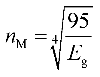 , with the ‘k’ value being 95 eV. The refractive loss is estimated using this relation in order to improve the solar cells' conversion parameter.55 The modified relation was proposed by Ravindra,56 according to which the difference between the average and optical energy gaps is constant. It can be expressed as: nR = 4.084 − [0.62 × Eg]. Moss confirmed the relationship and stated that it holds valid for bandgaps smaller than 4 eV. This will display erroneous values for both extremely low and high bandgap values. However, for low energy gap materials, Herve–Vandamme57 put forward the model based on oscillator theory. The relation is expressed as:
 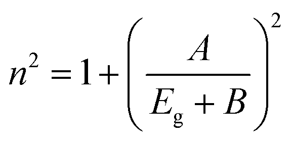 , with A being the ionization energy of hydrogen = 13.6 eV and B = 3.74 eV. The rewritten form of the equation is:
 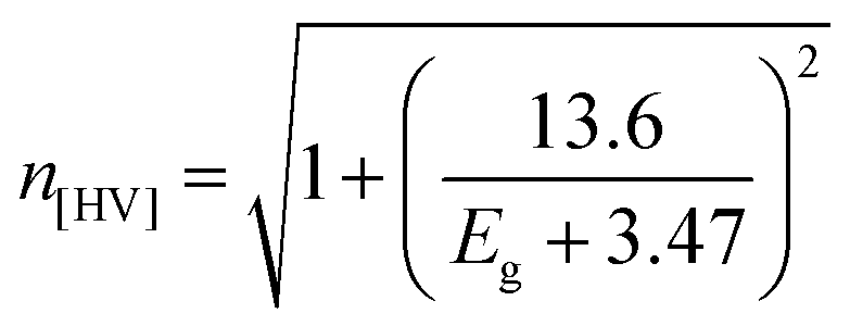 . Another relationship between n and Eg was also suggested by Tripathy.58 It is based on the exponential decay relation between ‘n’ and ‘Eg’ as: nT = 1.73 × [1 + 1.9017 × e−0.539×Eg].

 and are given in Table 2. The values are 3.62 × 10⁻¹⁰ esu, 3.90 × 10⁻¹⁰ esu and 3.96 × 10⁻¹⁰ esu for as-grown and 473 K and 523 K annealed films, respectively. The increased n2 value upon annealing is suitable for nonlinear device fabrication. The existence of significant nonlinearities presents an opportunity to develop compact and energy-efficient devices for telecommunications. The feasibility of creating small, low-power telecommunications devices is enhanced, as larger nonlinearity requires less energy and results in shorter interaction lengths.62,63
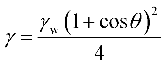 with γw = 71.99 mN m−1 (surface tension of water). The calculated values of γse are 0.58, 6.47 and 5.99 for as-grown and 473 K and 523 K annealed films. The thermal induced hydrophilicity of the material mostly increased due to the surface structure, change in the surface roughness and sometimes due to the oxygen vacancy sites. In the current case, the surface structure and surface roughness seemed to remain the same for annealed films, which shows the healing of atomic impairment. Fig. 9(d) shows a comparative plot between the contact angle and surface energy of the as-grown and annealed thin films.66