DOI:
10.1039/D3MA01032E
(Paper)
Mater. Adv., 2024,
5, 1746-1755
Hole doping at Sn sublattice of the buckled honeycomb SnX (X = S and Se) monolayer: an efficient functionalization approach†
Received
21st November 2023
, Accepted 8th January 2024
First published on 9th January 2024
Abstract
In this work, hole doping at the Sn sublattice is explored to induce feature-rich electronic and magnetic properties in SnX (X = S and Se) monolayers. In the buckled honeycomb structure, SnX monolayers exhibit good dynamical and thermal stability. Calculations indicate the non-magnetic semiconductor nature of SnS and SnSe monolayers with energy gaps of 2.31(3.01) and 2.21(2.88) eV, respectively, obtained using the PBE(HSE06) functional. A single Sn vacancy results in the emergence of half-metallicity with a total magnetic moment of 2.00, where the X atoms closest to the defect site mainly produce the magnetic properties. Similarly, the half-metallic nature is induced by doping with IA-group (Li and Na) atoms, however the magnetization is weaker with total magnetic moments between 0.95 and 1.00 μB. Herein, the magnetism is originated mainly from the p orbitals of chalcogen X atoms closest to the doping site. On the other hand, magnetic semiconductor nature emerges as a consequence of incorporating IIIA-group (Ga and In atoms) impurities. In these cases, a total magnetic moment of 1.00 μB is obtained, where impurities and their neighbor atoms play a key role in the monolayer magnetization. The density of states spectra and Bader charge analysis indicate ionic chemical bonds between Li(Na) atoms and X atoms, while the Ga(In)–X chemical bonds are a mix of covalent and ionic characters. The results presented herein may introduce the defected and doped SnX monolayers as prospective two-dimensional (2D) spintronic materials, such that hole doping can be considered as an efficient approach to functionalize SnX monolayers.
I. Introduction
Since its first successful exfoliation,1 graphene has become one of the most interesting two-dimensional (2D) materials due to its intriguing mechanical, physical, and chemical features.2,3 So far, graphene has emerged as revolutionizing not only high-performance nanoelectronics and nanooptoelectronics, but it has been also explored as a promising 2D material for catalysis,4,5 energy storage,6,7 biomedical8,9 and environmental applications,10,11 gas sensing,12,13 and spintronics,14,15 among others. However, this 2D material has a shortcoming of having a zero gap that causes a significant limitation in its use in optoelectronic and electronic nanodevices, and requires huge research efforts into graphene band gap opening.16–18 Along with graphene, a large variety of 2D semiconductors and insulators have been prepared in experiments as prospective alternatives to graphene, such as boron nitride (BN),19,20 phosphorene,21,22 transition metal dichalcogenides,23–26 pnictogens,27,28 and metal oxides.29 Besides experimental investigations, researchers have paid special attention to predicting novel 2D materials using physicochemical theories and advancing computing technology. So far, a large variety of 2D materials have been treated using first-principles calculations, which covers from the structural stability and basic properties to device performances. 2D materials can be categorized considering their chemical composition as those of I–VII group,30,31 II–VI group,32,33 III–V group,34,35 IV–IV group,35–37 IV–VI group,38–40 and V–V group (pnictogens).41,42
Belonging to the IV–VI group family, tin monochalcogenides are abundant and of low cost, and environmentally friendly. These materials are promising candidates for thermoelectric, solar energy conversion, and photovoltaic applications.43–45 Between them, SnX (X = S and Se) compounds have high light absorption efficiency due to their optimal band gap about 1.3 eV.46 In the context of rapid development of nanoscience and nanotechnology, 2D counterparts of SnX compounds have been investigated both experimentally and theoretically. For instance, single layer with four-atomic thickness SnSe nanosheets have been prepared by Li et al.47 The optoelectronic characterizations indicate great applicability of ultrathin SnSe nanosheets in photodetector and photovoltaic devices. So far, various research groups have demonstrated high performance of SnX monolayers for photocatalysis,48,49 piezoelectricity,50,51 and thermoelectrics,52,53 and so on. Ul Haq et al.54 have explored different polymorphs of single layered SnSe, where the buckled honeycomb phase has the largest band gap of 2.32 eV calculated at the level of TB-mBJ exchange potential. To the best of our knowledge, most investigations focus on the orthorhombic structure,55,56 while the buckled honeycomb receives much less attention despite its versatility for 2D materials.
Nowadays, spintronic devices (spin-based electronics) have been rapidly replacing the silicon-based traditional electronic devices,57,58 which are widely used in data storage, transforming information, coding and decoding, among others. Half-metallic and magnetic semiconductor natures are two typical spintronic materials properties, which take advantage of the spin-polarized electronic states to generate high-performance spin current.59–62 It has been found that most 2D materials are non-magnetic in the ground state, therefore different methods have been explored to get appropriate magnetization. A common way is to create vacancies that can be realized experimentally by high energy atom or ion bombardment. Then, a further doping process is carried out by filling vacancies with desired dopants.63,64 Motivated by the search for new 2D spintronic materials, the effects of vacancy and hole doping on the SnX (X = S and Se) monolayers’ electronic and magnetic properties are investigated in this work. Herein, Li and Na (IA-group) atoms, Mg and Ca (IIA-group) atoms, and Ga and In (IIIA-groups) atoms are selected as dopants due to their similar atomic size in comparison with the Sn atom.65 It is anticipated that SnX monolayers are significantly magnetized by creating a Sn vacancy and doping with IA- and IIIA-group atoms, where either a half-metallicity or magnetic semiconductor nature is induced. In contrast, IIA-group impurities preserve the non-magnetic state with negligible band gap variation (see Fig. S2 of the ESI†). Therefore, results of the Li-, Na-, Ga-, and In-doped SnX monolayers are reported in the main text of this paper.
II. Computational details
All the first-principles calculations on the pristine, vacancy-defected, and doped SnX (X = S and Se) monolayers are performed using the Vienna Ab initio Simulation Package (VASP),66,67 which is based on density functional theory (DFT).68 The electronic exchange–correlation energy is treated with the Perdew–Burke–Ernzerhof generalized gradient approximation (GGA-PBE),69 while the all-electron projector augmented wave (PAW) method is employed to describe the ion—electron interactions. The cutoff energy for the plane wave basis set is always set to 500 eV. As the convergence criterion, the difference in self-consistent total energy is within 10−6 eV. During the structural relaxation, the force is less than 0.01 eV Å−1. A Γ-centered Monkhorst–Pack k-point grid70 of 20 × 20 × 1 is used for pristine monolayers (unit cell), meanwhile a 4 × 4 × 1 mesh is generated for the Brillouin zone integration of the doped systems (4 × 4 × 1 supercell). A vacuum gap wider than 14 Å is added between monolayer planes to avoid the interactions between the perpendicularly periodic images.
III. Results and discussion
A. Pristine SnX (X = S and Se) monolayers
Herein, SnX (X = S and Se) monolayers are predicted adopting the buckled hexagonal structure that is ascribed to the P3m1 space group (no. 156). The unit cell, containing one Sn atom and one X atom, is displayed in Fig. 1a and b. Each atomic species is located in a separated plane to form the structural wrinkle. After relaxation, the following structural parameters are obtained for the SnS/SnSe monolayers optimized structures: (1) lattice constant a = 3.75/3.91 Å; (2) buckling height ΔSn–X = 1.46/1.56 Å; (3) chemical bond length dSn–X = 2.61/2.75 Å; and (4) interatomic angles ∠SnXSn = ∠XSnX = 91.66°/90.78°. The differences in these parameters are originated from the atomic sizes, the larger atomic size of the Se atom in comparison with that of the S atom induces a larger lattice constant, buckling height and chemical bond length, and smaller interatomic angles. Further, the stability of the optimized structures is examined. Fig. 1c shows the phonon dispersion curves of SnX monolayers, where no imaginary phonon frequency is observed. This feature indicates that both SnS and SnSe monolayers are dynamically stable. The snapshots of structures at 300 K calculated by ab initio molecular dynamic (AIMD) simulations are given in Fig. 1d (see Fig. S1, ESI† for the fluctuation of energy and visualization of structure after simulations). After 5 ps (1000 steps), the constituent atoms move slightly from their equilibrium sites, and no geometric reconstructions and/or broken bonds are noticed. Results indicate good thermal stability of the SnS and SnSe monolayers.
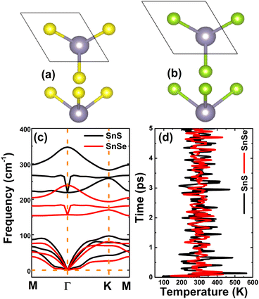 |
| | Fig. 1 Atomic structure of (a) SnS and (b) SnSe (Sn atom: grey ball; S atom: yellow ball; Se atom: green ball; a unit cell is marked); and their (c) phonon dispersion curves and (d) AIMD simulations at 300 K (temperature fluctuations; see Fig. S1 for energy fluctuations and the visualization of atomic structures after simulations). | |
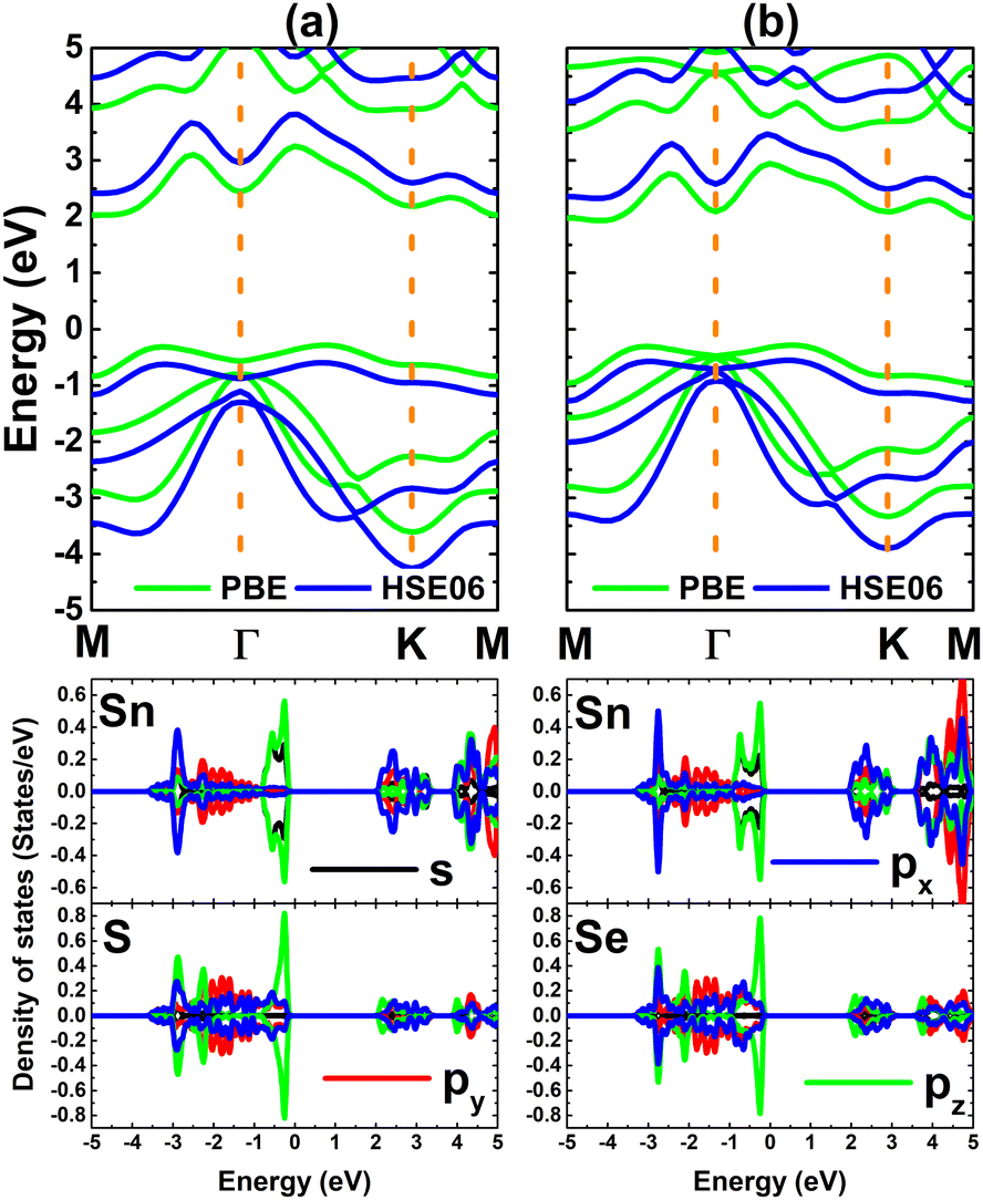
Fig. 2 shows the band structures of SnX monolayers calculated along the M–Γ–K–M in-plane direction using the PBE functional and HSE06 hybrid functional. The latter is employed in order to get a more accurate band gap prediction due to the 25% fraction of the exact Hartree–Fock exchange potential.71 Note that both functionals assert an indirect gap semiconductor nature of the considered 2D materials, where the valence band maximum and conduction band minimum take place along the ΓK direction and at the M point, respectively. The PBE functional yields energy gaps of 2.31 and 2.21 eV for the SnS and SnSe monolayer, respectively. As expected, larger values of 3.01 and 2.88 eV, respectively, are obtained from HSE06-based calculations. Further, the projected density of states (PDOS) spectra are also given to get more insight into the SnX monolayers’ band structure formation. It can be noted that the upper part of the valence band is formed by Sn-s, Sn-pz and X-pz states, while px and py states of all the constituent atoms originate the lower part. In the considered energy range, the conduction band is built mainly by Sn-px and Sn-py states, where a smaller contribution from chalcogen atoms is also observed. The PDOS profiles may suggest significant electronic hybridization between Sn and X atoms in both monolayers to generate the covalent chemical bonds. However, the difference in electronegativity causes also the charge transfer from the Sn atom to X atom. To quantify this process, the Bader charge analysis is performed. Results indicate that S and Se atoms gain charge amounts of 0.79 and 0.66 e from the Sn atom, respectively. A larger quantity is transferred to the S atom due to its more electronegative nature than the Se atom. These results may indicate also an important fraction of ionic character in Sn–X chemical bonds, which are the results of the charge transfer. Such that, it can be concluded that the chemical bonds in SnX monolayers are a mix of covalent and ionic characters.
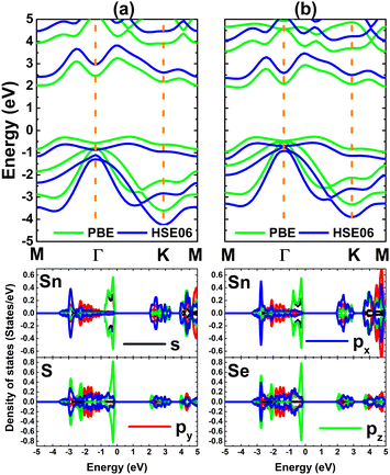 |
| | Fig. 2 Electronic band structure (the Fermi level is set to 0 eV) and projected density of states of (a) SnS and (b) SnSe monolayer. | |
B. Effects of single Sn vacancy
The effects of a single Sn vacancy in SnX monolayers are investigated using a 4 × 4 × 1 supercell, which are now denoted by Sn31X32. The formation energy Ef is calculated as follows:| | | Ef = Et(Sn31X32) − Et(Sn32X32) + μSn | (1) |
where Et(Sn31X32) and Et(Sn32X32) are total energy of the defected and perfect monolayer, respectively; μSn is the chemical potential of the Sn atom calculated from its most stable bulk phase. According to our calculations, Ef values of 2.76 and 2.51 eV are required to create a single Sn vacancy in SnS and SnSe monolayers, respectively. Then, cohesive energy values, Ec, of the defected systems are determined to check the structural-chemical stability using the following expression:| |  | (2) |
herein, Et is total energy of the considered system; na and E(a) denote number of atom a in the system and energy of an isolated atom a, respectively. Simulations yield Ec values of −3.51 and −3.28 eV per atom for the Sn31S32 and Sn31Se32 system, respectively. The negative feature of the cohesive energy suggests good structural-chemical stability of SnX monolayers upon creating a single Sn vacancy. However, these values are less negative than that of perfect SnX monolayers (−3.60 and −3.36 eV per atom of SnS and SnSe monolayer, respectively), indicating that the presence of the vacancy reduces slightly the structural-chemical stability of the considered monolayers.
It has been found that SnX monolayers are significantly magnetized by creating a single Sn vacancy. The appearance of magnetism is demonstrated by a total magnetic moment of 2.00 μB in both cases. Spin density in the defected SnX monolayers is illustrated in Fig. 3 to get more insights into the origin of the magnetism. It can be noted that the spin surfaces are centered mainly at S and Se atoms closest to the vacancy site, indicating their main contribution to the magnetic properties. Undoubtedly, the magnetization is derived from the partial occupancy of the outermost S-3p and Se-4p orbitals, which is a consequence of the loss of the removed charge (Sn atom).
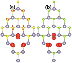 |
| | Fig. 3 Spin density (iso-surface value: 0.005 e Å−3) in (a) SnS and (b) SnSe monolayer with a single Sn vacancy. | |
The magnetism in SnX monolayers is also reflected in the spin-polarized band structures, which are displayed in Fig. 4. Note that the spin polarization takes place mainly in the vicinity of the Fermi level. The semiconductor character is preserved in the spin-up state with energy gap of 2.14 and 2.08 eV for the vacancy-defected SnS and SnSe monolayer, respectively. Meanwhile, new middle-gap states emerge overlapping with the Fermi level to metallize the spin-down state. These band structure profiles suggest the creation of a single Sn vacancy as an efficient method to functionalize SnX monolayers for spintronic applications, in which the half-metallic nature is induced to make new 2D materials for spin current generation.72
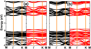 |
| | Fig. 4 Spin-resolved band structure (the Fermi level is set to 0 eV; spin-up: black curve; spin-down: red curve) of (a) SnS and (b) SnSe monolayer with a single Sn vacancy. | |
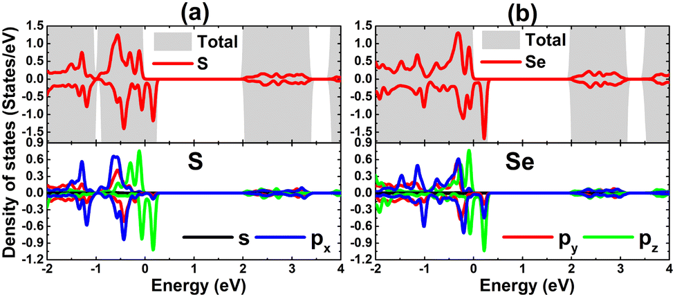
The total and projected density of states of S and Se atoms around the Fermi level are given in Fig. 5 to analyze with more detail their contribution to the defected SnS and SnSe monolayers’ electronic and magnetic properties. In the considered energy range, the valence band is formed mainly by the X-p orbital that exhibits the spin polarization as expected due to its important role in the system’s magnetization (with only partial occupancy). The spin-down metallization is induced mainly by S-pz and Se-pz states (with a small contribution from the Se-px state). Meanwhile, the spin-up channel is quite similar to that of the perfect monolayer, where the pz state dominates the upper part of the valence band.
 |
| | Fig. 5 Total and projected density of states of atoms closest to the vacancy site in (a) SnS and (b) SnSe monolayer with a single Sn vacancy. | |
C. Effects of doping with IA-group (Li and Na) atoms
In this part, the effects of doping with IA-group (Li and Na) atoms on the SnX monolayers’ electronic and magnetic properties are investigated by substituting one Sn atom in a 4 × 4 × 1 supercell by one IA-group atom. The doped systems are denoted by Sn31D1X32 (D = Li and Na). Firstly, the doping energy Ed is calculated as follows:| | | Ed = Et(Sn31D1X32) − Et(Sn32X32) + μSn − μD | (3) |
where Et(Sn31D1X32) and Et(Sn32X32) denote total energy of the doped and bare monolayer, respectively; μSn and μD are the chemical potential of Sn and the dopant atom, respectively, which are calculated from their most stable bulk structure. Results are listed in Table 1. Doping energies of −0.35 and −0.15 eV are obtained for doping Li in the SnS and SnSe monolayer, respectively. Negative Ed values suggest an exothermic Li doping process. In contrast, Na doping is an endothermic process as suggested by the positive Ed values of 0.21 and 0.23 eV, respectively. Note that doping in the SnS monolayer is energetically more favorable than in the SnSe monolayer as asserted by its more negative doping energy. Then, using eqn (2), negative cohesive energy Ec values between −3.28 and −3.56 eV per atom are obtained for SnX monolayers doped with IA-group atoms (see Table 1), indicating good structural-chemical stability of the doped systems. It is worth mentioning that the doping reduces slightly the stability since Ec becomes more positive (from −3.60 eV per atom of the bare monolayer).
Table 1 Doping energy Ed (eV), cohesive energy Ec (eV), electronic band gap Eg (eV; spin-up/spin-down; M: metallic), charge transferred from impurity ΔQ (e), and total magnetic moment Mt (μB) of the atom-doped SnX (X = S and Se) monolayer
|
|
SnS |
SnSe |
|
E
d
|
E
c
|
E
g
|
ΔQ |
M
t
|
E
d
|
E
c
|
E
g
|
ΔQ |
M
t
|
| Li-doped |
−0.35 |
−3.56 |
2.22/M |
0.85 |
0.98 |
−0.15 |
−3.31 |
2.09/M |
0.84 |
0.95 |
| Na-doped |
0.21 |
−3.52 |
2.22/M |
0.79 |
1.00 |
0.23 |
−3.28 |
2.09/M |
0.79 |
1.00 |
| Ga-doped |
0.42 |
−3.57 |
1.27/1.80 |
0.70 |
1.00 |
0.51 |
−3.33 |
1.36/1.59 |
0.56 |
1.00 |
| In-doped |
0.39 |
−3.55 |
1.56/1.41 |
0.70 |
1.00 |
0.38 |
−3.32 |
1.53/1.30 |
0.59 |
1.00 |
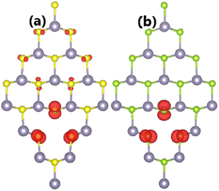
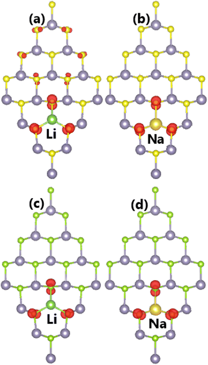
Our calculations demonstrate that doping with Li and Na atoms significantly magnetizes SnX monolayers. Such that total magnetic moments of 0.98 and 0.95 μB are obtained for Li-doped SnS and SnSe monolayers, respectively. Besides, the Na impurity induces a total magnetic moment of 1.00 μB in both monolayers. Fig. 6 illustrates the spin density in doped systems to investigate the origin of the magnetism. From the figure, it can be concluded that magnetic properties are produced mainly by the S and Se atoms closest to the doping site provided that spin surfaces are centered mainly at their sites. Remembering that the substitutional incorporation of Li and Na atoms induces two holes, such that the outermost orbital of X atoms (only neighbor atoms of dopants are affected) is not fulfilled. Consequently, the magnetism appears as a result of their partial occupancy.
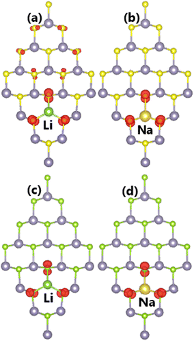 |
| | Fig. 6 Spin density (iso-surface value: 0.003 e Å−3) in (a–b) SnS and (c–d) SnSe monolayer doped with Li and Na atoms. | |
The calculated spin-polarized band structures of SnX monolayers doped with Li and Na are displayed in Fig. 7, which indicate their half-metallic nature. Similar to previous cases of single Sn vacancy, the spin-up states exhibit semiconductor character with energy gaps of 2.22 and 2.09 eV for Li/Na-doped SnS and SnSe monolayers, respectively. Meanwhile, the spin-down state is metallized with significant overlapping of the new middle-gap state with the Fermi level. Due to their feature-rich half-metallicity, SnX monolayers doped with IA-group atoms can be recommended as prospective spintronic 2D materials, where the doping leads to the emergence of significant d0 magnetism in non-magnetic host monolayers.
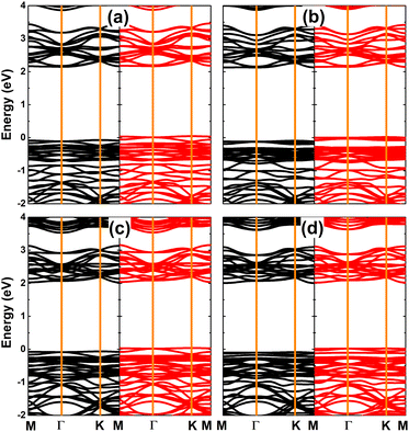 |
| | Fig. 7 Spin-resolved band structure (the Fermi level is set to 0 eV; spin-up: black curve; spin-down: red curve) of SnS monolayer doped with (a) Li and (b) Na atom; and SnSe monolayer doped with (c) Li and (d) Na atom. | |
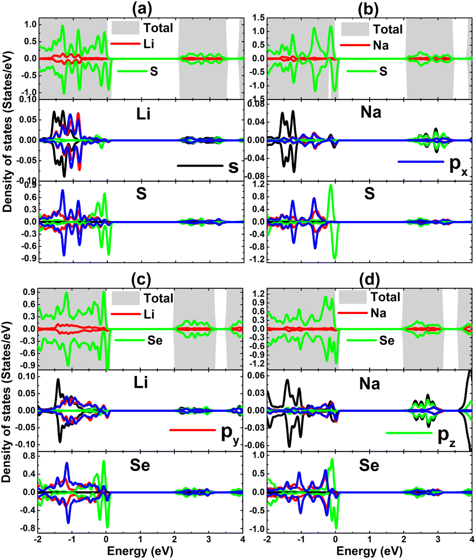
TDOS and PDOS spectra of IA-group impurities and their neighbor X atoms are given in Fig. 8 to analyze their contributions to electronic and magnetic properties. Note that impurities (with s, px, py, and pz states) contribute to the formation of the lower part of the valence band and conduction band, which is a characteristic of cation species in compounds. The lower part of the valence band is formed also by X-px and X-py states, while the X-pz state originates mainly the upper part. This latter state is also responsible for the spin-down metallization. PDOS spectra indicate that magnetism is produced mainly by the X-pz state considering its significant spin polarization. Moreover, the weak electronic hybridization suggests that the chemical bond between Li and Na impurities and their neighboring chalcogen atoms is predominantly ionic, which is formed by the charge transfer. The Bader charge analysis asserts that charge quantities of 0.85/0.79 and 0.84/0.79 e are transferred from the Li/Na dopant to the host SnS and SnSe monolayer, respectively.
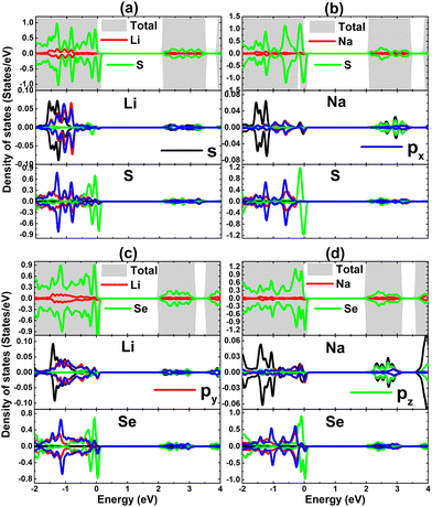 |
| | Fig. 8 Total and projected density of states of impurities and their neighbor atoms of SnS monolayer doped with (a) Li and (b) Na atom; and SnSe monolayer doped with (c) Li and (d) Na atom. | |
D. Effects of doping with IIIA-group (Ga and In) atoms
Now, the SnX monolayers doped with IIIA-group (Ga and In) atoms are investigated using a 4 × 4 × 1 supercell as for the previous cases. Using eqn (3) for these cases, Ed values of 0.42/0.39 and 0.51/0.38 eV are obtained for doping Ga/In in SnS and SnSe monolayers, respectively. Note that In doping requires supplying less energy than Ga doping, which is a result of the similar atomic size of the In impurity to the removed Sn atom. Once formed, all the doped SnX monolayers are proven to be structurally and chemically stable considering their negative cohesive energies between −3.57 and −3.32 eV per atom. Note that these values are less negative than that of bare SnX monolayers (−3.60 eV per atom), indicating a slight reduction in stability.
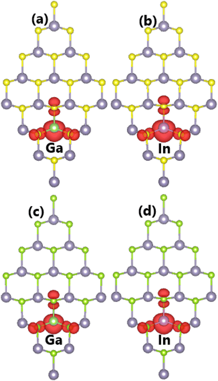
It is found that the ground state of Sn31D1X32 (D = Ga and In) systems is magnetic at total magnetic moment of 1.00 μB. This result demonstrates that SnX monolayers are significantly magnetized by doping with IIIA-group (Ga and In) atoms. Further, the illustration of spin density in Fig. 9 indicates that magnetic properties are produced by impurities and their neighboring chalcogen atoms. Unlike the previous cases of doping with Li and Na atoms, the Ga and In dopants make an important contribution to the magnetic properties. This feature may be derived from the electronic hybridization, which will be analyzed in more detail below.
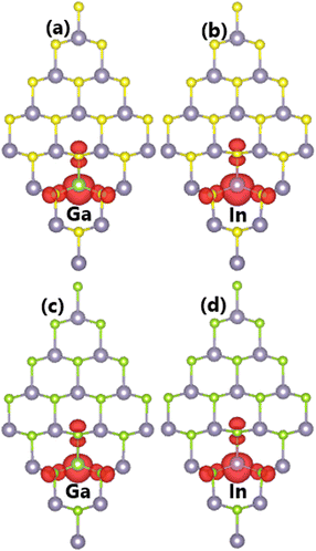 |
| | Fig. 9 Spin density (iso-surface value: 0.003 e Å−3) in (a–b) SnS and (c–d) SnSe monolayer doped with Ga and In atoms. | |
Fig. 10 shows the spin-polarized band structures of SnX monolayers doped with Ga and In. It can be seen that the lower part of the valence band and upper part of the conduction band are quite spin-symmetric. However, the spin symmetry is broken around the Fermi level with the appearance of new middle-gap flat energy branches: one spin-up below the Fermi level and the other spin-down above the Fermi level, such that the semiconductor behavior is preserved in both spin configurations. The band structure profiles indicate that doping with IIIA-group atoms leads to the emergence of the magnetic semiconductor in SnX monolayers to make them prospective spintronic materials.61 The spin-dependent energy gaps are listed in Table 1.
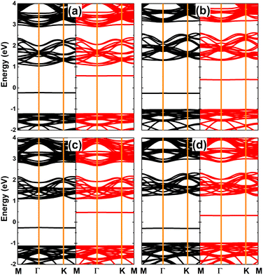 |
| | Fig. 10 Spin-resolved band structure (the Fermi level is set to 0 eV; spin-up: black curve; spin-down: red curve) of SnS monolayer doped with (a) Ga and (b) In atom; and SnSe monolayer doped with (c) Ga and (d) In atom. | |
The contribution of IIIA-group impurities and their neighboring X atoms are analyzed through TDOS and PDOS spectra displayed in Fig. 11. Note that the middle-gap states are formed mainly by the hybridization between impurities and their neighbor X atoms. Specifically, Ga(In)-s–pz states and X-px–pz states hybridize significantly in the vicinity of the Fermi level, making contributions to the formation of new middle-gap states. Therefore, it can be concluded that these mentioned electronic states originate mainly the magnetic properties of the doped systems and the hybridization is responsible for the SnX monolayers’ magnetization. The electronic hybridization between IIIA-group atoms and X atoms may suggest covalent bonds, however it will be flawed to not consider the ionic character caused by the charge transfer provided the difference in their electronegativity. Our Bader charge analysis shows that the host SnS and SnSe monolayers gain charge amounts of 0.70/0.70 and 0.56/0.59 e from the Ga/In dopant, respectively. Note that the SnS monolayer receives a larger quantity, which is due to the more electronegative character of the S atom compared to the Se atom.
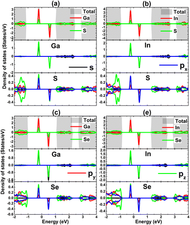 |
| | Fig. 11 Total and projected density of states of impurities and their neighbor atoms of SnS monolayer doped with (a) Ga and (b) In atom; and SnSe monolayer doped with (c) Ga and (d) In atom. | |
IV. Conclusions
In conclusion, the electronic and magnetic properties of pristine, vacancy-defected, and doped SnX (X = S and Se) monolayers have been investigated systematically using first-principles calculations. Phonon calculations and AIMD simulations assert good stability of the pristine monolayer. Moreover, electronic band structures indicate their non-magnetic semiconductor nature, where Sn and X atoms exhibit significant electronic hybridization in the valence band. Upon creating a single Sn vacancy, the monolayers are significantly magnetized and the half-metallicity is induced. The p orbital of S and Se atoms closest to the defect site originates mainly the magnetism due to its partial occupancy. Similar features are obtained by doping with Li and Na atoms, however the magnetization is weaker which is reflected in smaller total magnetic moments. In these cases, chalcogen atoms closest to the doping site regulate mainly the electronic and magnetic properties, where the contribution of IA-group impurities is quite small. The interactions between Li/Na atom and X atom are predominantly ionic due to the charge transfer process from the former to the latter. On the other hand, the strong hybridization between Ga(In) dopants and their neighbor X atoms originate new middle-gap energy states in both the valence band and conduction band with a strong spin polarization in the vicinity of the Fermi level. Consequently, the magnetic semiconductor nature is induced. The electronic hybridization suggests covalent Ga(In)–X chemical bonds, however the ionic character is also important due to the difference in their electronegativity. Since half-metallic and magnetic semiconductor natures are desirable for spintronic applications, the Sn vacancy creation and doping can be considered as efficient and solid ways to functionalize SnX monolayers.
Data availability
Data related to this study are available upon reasonable request.
Conflicts of interest
The authors declare that they have no known competing financial interests or personal relationships that could have appeared to influence the work reported in this paper.
Acknowledgements
Calculations were performed in the DGCTIC-UNAM Supercomputing Center (projects LANCAD-UNAM-DGTIC-368). D. M. Hoat expresses his gratitude for all the valuable support from Duy Tan University, which is going to celebrate its 30th anniversary of establishment (Nov. 11, 1994–Nov. 11, 2024) towards “Integral, Sustainable and Stable Development”.
References
- K. S. Novoselov, A. K. Geim, S. V. Morozov, D.-E. Jiang, Y. Zhang, S. V. Dubonos, I. V. Grigorieva and A. A. Firsov, Electric field effect in atomically thin carbon films, Science, 2004, 306(5696), 666–669 CrossRef CAS PubMed.
- C. Soldano, A. Mahmood and E. Dujardin, Production, properties and potential of graphene, Carbon, 2010, 48(8), 2127–2150 CrossRef CAS.
- M. J. Allen, V. C. Tung and R. B. Kaner, Honeycomb carbon: a review of graphene, Chem. Rev., 2010, 110(1), 132–145 CrossRef CAS PubMed.
- C. Huang, C. Li and G. Shi, Graphene based catalysts, Energy Environ. Sci., 2012, 5(10), 8848–8868 RSC.
- B. F. Machado and P. Serp, Graphene-based materials for catalysis, Catal. Sci. Technol., 2012, 2(1), 54–75 RSC.
- A. G. Olabi, M. A. Abdelkareem, T. Wilberforce and E. T. Sayed, Application of graphene in energy storage device-A review, Renewable Sustainable Energy Rev., 2021, 135, 110026 CrossRef CAS.
- M. Pumera, Graphene-based nanomaterials for energy storage, Energy Environ. Sci., 2011, 4(3), 668–674 Search PubMed.
- D. Bitounis, H. Ali-Boucetta, B. H. Hong, D.-H. Min and K. Kostarelos, Prospects and challenges of graphene in biomedical applications, Adv. Mater., 2013, 25(16), 2258–2268 CrossRef CAS PubMed.
- M. E. Foo and S. C. Gopinath, Feasibility of graphene in biomedical applications, Biomed. Pharmacother., 2017, 94, 354–361 CrossRef CAS PubMed.
- F. Perreault, A. F. De Faria and M. Elimelech, Environmental applications of graphene-based nanomaterials, Chem. Soc. Rev., 2015, 44(16), 5861–5896 Search PubMed.
- F. Li, X. Jiang, J. Zhao and S. Zhang, Graphene oxide: A promising nanomaterial for energy and environmental applications, Nano Energy, 2015, 16, 488–515 CrossRef CAS.
- S. S. Varghese, S. Lonkar, K. Singh, S. Swaminathan and A. Abdala, Recent advances in graphene based gas sensors, Sens. Actuators, B, 2015, 218, 160–183 CrossRef CAS.
- W. Yuan and G. Shi, Graphene-based gas sensors, J. Mater. Chem. A, 2013, 1(35), 10078–10091 Search PubMed.
- W. Han, R. K. Kawakami, M. Gmitra and J. Fabian, Graphene spintronics, Nat. Nanotechnol., 2014, 9(10), 794–807 CrossRef CAS PubMed.
- P. Seneor, B. Dlubak, M.-B. Martin, A. Anane, H. Jaffres and A. Fert, Spintronics with graphene, MRS Bull., 2012, 37(12), 1245–1254 Search PubMed.
- S. Sahu and G. Rout, Band gap opening in graphene: a short theoretical study, Int. Nano Lett., 2017, 7, 81–89 CrossRef CAS.
- X. Fan, Z. Shen, A. Liu and J.-L. Kuo, Band gap opening of graphene by doping small boron nitride domains, Nanoscale, 2012, 4(6), 2157–2165 RSC.
- M. Y. Han, B. Özyilmaz, Y. Zhang and P. Kim, Energy band-gap engineering of graphene nanoribbons, Phys. Rev. Lett., 2007, 98(20), 206805 CrossRef PubMed.
- K. K. Kim, A. Hsu, X. Jia, S. M. Kim, Y. Shi, M. Hofmann, D. Nezich, J. F. Rodriguez-Nieva, M. Dresselhaus and T. Palacios,
et al., Synthesis of monolayer hexagonal boron nitride on Cu foil using chemical vapor deposition, Nano Lett., 2012, 12(1), 161–166 CrossRef PubMed.
- Y. Gao, W. Ren, T. Ma, Z. Liu, Y. Zhang, W.-B. Liu, L.-P. Ma, X. Ma and H.-M. Cheng, Repeated and controlled growth of monolayer, bilayer and few-layer hexagonal boron nitride on Pt foils, ACS Nano, 2013, 7(6), 5199–5206 CrossRef CAS PubMed.
- L. Li, Y. Yu, G. J. Ye, Q. Ge, X. Ou, H. Wu, D. Feng, X. H. Chen and Y. Zhang, Black phosphorus field-effect transistors, Nat. Nanotechnol., 2014, 9(5), 372–377 Search PubMed.
- W. Zhang, H. Enriquez, Y. Tong, A. Bendounan, A. Kara, A. P. Seitsonen, A. J. Mayne, G. Dujardin and H. Oughaddou, Epitaxial synthesis of blue phosphorene, Small, 2018, 14(51), 1804066 CrossRef PubMed.
- Y. Yu, C. Li, Y. Liu, L. Su, Y. Zhang and L. Cao, Controlled scalable synthesis of uniform, high-quality monolayer and few-layer MoS2 films, Sci. Rep., 2013, 3(1), 1866 CrossRef PubMed.
- X. Lu, M. I. B. Utama, J. Lin, X. Gong, J. Zhang, Y. Zhao, S. T. Pantelides, J. Wang, Z. Dong and Z. Liu,
et al., Large-area synthesis of monolayer and few-layer MoSe2 films on SiO2 substrates, Nano Lett., 2014, 14(5), 2419–2425 Search PubMed.
- K. M. McCreary, A. T. Hanbicki, G. G. Jernigan, J. C. Culbertson and B. T. Jonker, Synthesis of large-area WS2 monolayers with exceptional photoluminescence, Sci. Rep., 2016, 6(1), 19159 Search PubMed.
- J.-K. Huang, J. Pu, C.-L. Hsu, M.-H. Chiu, Z.-Y. Juang, Y.-H. Chang, W.-H. Chang, Y. Iwasa, T. Takenobu and L.-J. Li, Large-area synthesis of highly crystalline WSe2 monolayers and device applications, ACS Nano, 2014, 8(1), 923–930 CrossRef CAS PubMed.
- M. Pumera and Z. Sofer, 2D monoelemental arsenene, antimonene, and bismuthene: beyond black phosphorus, Adv. Mater., 2017, 29(21), 1605299 Search PubMed.
- Y. Hu, J. Liang, Y. Xia, C. Zhao, M. Jiang, J. Ma, Z. Tie and Z. Jin, 2D arsenene and arsenic materials: Fundamental properties, preparation, and applications, Small, 2022, 18(9), 2104556 CrossRef CAS PubMed.
- H. Zhang, M. Holbrook, F. Cheng, H. Nam, M. Liu, C.-R. Pan, D. West, S. Zhang, M.-Y. Chou and C.-K. Shih, Epitaxial growth of two-dimensional insulator monolayer honeycomb BeO, ACS Nano, 2021, 15(2), 2497–2505 CrossRef CAS PubMed.
- H. A. Huy, D. K. Nguyen, C. V. Ha, D. D. Toan, H. N. Nguyen, J. G. Sanchez and D. Hoat, Functionalization of an ionic honeycomb KF monolayer via doping, Nanoscale Adv., 2023, 5(17), 4480–4488 Search PubMed.
- M.-Y. Ma, N.-K. Chen, D. Wang, D. Han, H.-B. Sun, S. Zhang and X.-B. Li, Defect physics in 2D monolayer I-VII semiconductor AgI, Mater. Today Nano, 2023, 22, 100304 CrossRef CAS.
- H. Zheng, X.-B. Li, N.-K. Chen, S.-Y. Xie, W. Q. Tian, Y. Chen, H. Xia, S. Zhang and H.-B. Sun, Monolayer II-VI semiconductors: A first-principles prediction, Phys. Rev. B: Condens. Matter Mater. Phys., 2015, 92(11), 115307 CrossRef.
- M. M. Alyörük, Piezoelectric properties of monolayer II-VI group oxides by first-principles calculations, Phys. Status Solidi B, 2016, 253(12), 2534–2539 CrossRef.
- X.-F. Liu, Z.-J. Luo, X. Zhou, J.-M. Wei, Y. Wang, X. Guo, B. Lv and Z. Ding, Structural, mechanical, and electronic properties of 25 kinds of III-V binary monolayers: A computational study with first-principles calculation, Chin. Phys. B, 2019, 28(8), 086105 Search PubMed.
- H. Sahin, S. Cahangirov, M. Topsakal, E. Bekaroglu, E. Akturk, R. T. Senger and S. Ciraci, Monolayer honeycomb structures of group-IV elements and III-V binary compounds: First-principles calculations, Phys. Rev. B: Condens. Matter Mater. Phys., 2009, 80(15), 155453 CrossRef.
- A. Baradaran and M. Ghaffarian, Topological viewpoint of two-dimensional group III-V and IV-IV compounds in the presence of electric field and spin-orbit coupling by density functional theory and tight-binding model, J. Phys.: Condens. Matter, 2022, 34(14), 145502 Search PubMed.
- Y. Mogulkoc, M. Modarresi, A. Mogulkoc, Y. Ciftci and B. Alkan, First principle and tight-binding study of strained SnC, J. Phys. Chem. Solids, 2017, 111, 458–463 CrossRef CAS.
- C. Kamal, A. Chakrabarti and M. Ezawa, Direct band gaps in group IV–VI monolayer materials: Binary counterparts of phosphorene, Phys. Rev. B, 2016, 93(12), 125428 Search PubMed.
- S.-D. Guo and Y.-H. Wang, Thermoelectric properties of orthorhombic group IV–VI monolayers from the first-principles calculations, J. Appl. Phys., 2017, 121(3), 034302 CrossRef.
- Y. Zengin, R. Caglayan and Y. Mogulkoc, Adsorption of small gas molecules onto the two-dimensional Janus SnSSe monolayer, Comput. Condens. Matter, 2023, 36, e00815 CrossRef.
- S. Ghosal, S. Chowdhury and D. Jana, Impressive thermoelectric figure of merit in two-dimensional tetragonal pnictogens: A combined first-principles and machine-learning approach, ACS Appl. Mater. Interfaces, 2021, 13(49), 59092–59103 CrossRef CAS PubMed.
- P. K. Roy, J. Luxa and Z. Sofer, Emerging pnictogen-based 2D semiconductors: sensing and electronic devices, Nanoscale, 2020, 12(19), 10430–10446 RSC.
- Y.-M. Han, J. Zhao, M. Zhou, X.-X. Jiang, H.-Q. Leng and L.-F. Li, Thermoelectric performance of SnS and SnS-SnSe solid solution, J. Mater. Chem. A, 2015, 3(8), 4555–4559 RSC.
- E. Barrios-Salgado, L. A. Rodríguez-Guadarrama, M. L. Ramón García, L. G. Martínez, M. Nair and P. Nair, Thin film solar cells of cubic structured SnS-SnSe, Phys. Status Solidi A, 2017, 214(10), 1700036 CrossRef.
- B. Pejjai, V. R. M. Reddy, S. Gedi and C. Park, Status review on earth-abundant and environmentally green Sn-X (X= Se, S) nanoparticle synthesis by solution methods for photovoltaic applications, Int. J. Hydrogen Energy, 2017, 42(5), 2790–2831 CrossRef CAS.
- A. K. Deb and V. Kumar, Bandgap engineering in semiconducting one to few layers of SnS and SnSe, Phys. Status Solidi B, 2017, 254(2), 1600379 CrossRef.
- L. Li, Z. Chen, Y. Hu, X. Wang, T. Zhang, W. Chen and Q. Wang, Single-layer single-crystalline SnSe nanosheets, J. Am. Chem. Soc., 2013, 135(4), 1213–1216 CrossRef CAS PubMed.
- Y. Xu, K. Xu, C. Ma, Y. Chen, H. Zhang, Y. Liu and Y. Ji, Novel two-dimensional β-GeSe and β-SnSe semiconductors: anisotropic high carrier mobility and excellent photocatalytic water splitting, J. Mater. Chem. A, 2020, 8(37), 19612–19622 Search PubMed.
- X. Li, X. Zuo, X. Jiang, D. Li, B. Cui and D. Liu, Enhanced photocatalysis for water splitting in layered tin chalcogenides with high carrier mobility, Phys. Chem. Chem. Phys., 2019, 21(14), 7559–7566 RSC.
- R. Fei, W. Li, J. Li and L. Yang, Giant piezoelectricity of monolayer group IV monochalcogenides: SnSe, SnS, GeSe, and GeS, Appl. Phys. Lett., 2015, 107(17), 173104 CrossRef.
- A. I. Lebedev, Ferroelectricity and piezoelectricity in monolayers and nanoplatelets of SnS, J. Appl. Phys., 2018, 124(16), 164302 Search PubMed.
- R. Gupta, B. Dongre, J. Carrete and C. Bera, Thermoelectric properties of the SnS monolayer: Fully ab initio and accelerated calculations, J. Appl. Phys., 2021, 130(5), 054301 CrossRef CAS.
- Z.-Y. Hu, K.-Y. Li, Y. Lu, Y. Huang and X.-H. Shao, High thermoelectric performances of monolayer SnSe allotropes, Nanoscale, 2017, 9(41), 16093–16100 RSC.
- B. Ul Haq, S. AlFaify, R. Ahmed, F. K. Butt, A. Laref and M. Shkir, Exploring single-layered SnSe honeycomb polymorphs for optoelectronic and photovoltaic applications, Phys. Rev. B, 2018, 97(7), 075438 CrossRef.
- H. Ullah, H. J. Kim and Y.-H. Shin,
et al., Influences of vacancy and doping on electronic and magnetic properties of monolayer SnS, J. Appl. Phys., 2018, 124(6), 065102 CrossRef.
- M. Kar, B. Rajbanshi, S. Pal and P. Sarkar, Engineering the electronic structure of tin sulfide nanoribbons: A computational study, J. Phys. Chem. C, 2018, 122(10), 5731–5741 CrossRef CAS.
- A. Hirohata, K. Yamada, Y. Nakatani, I.-L. Prejbeanu, B. Diény, P. Pirro and B. Hillebrands, Review on spintronics: Principles and device applications, J. Magn. Magn. Mater., 2020, 509, 166711 CrossRef CAS.
- S. Wolf, D. Awschalom, R. Buhrman, J. Daughton, V. S. von Molnár, M. Roukes, A. Y. Chtchelkanova and D. Treger, Spintronics: a spin-based electronics vision for the future, Science, 2001, 294(5546), 1488–1495 CrossRef CAS PubMed.
- A. Ghosh, M. Kar, C. Majumder and P. Sarkar, First-principles calculations to investigate electronic structure and transport properties of CrC monolayers: A new horizon for spintronic application, Mater. Sci. Eng., B, 2021, 272, 115379 CrossRef CAS.
- A. Ghosh, M. Kar, C. Majumder and P. Sarkar, Half metallicity and ferromagnetism of vanadium nitride nanoribbons: a first-principles study, Phys. Chem. Chem. Phys., 2021, 23(2), 1127–1138 RSC.
- X. Li and J. Yang, First-principles design of spintronics materials, Natl. Sci. Rev., 2016, 3(3), 365–381 CrossRef CAS.
- Y.-W. Son, M. L. Cohen and S. G. Louie, Half-metallic graphene nanoribbons, Nature, 2006, 444(7117), 347–349 CrossRef CAS PubMed.
- H. Wang, Q. Wang, Y. Cheng, K. Li, Y. Yao, Q. Zhang, C. Dong, P. Wang, U. Schwingenschlogl and W. Yang,
et al., Doping monolayer graphene with single atom substitutions, Nano Lett., 2012, 12(1), 141–144 CrossRef CAS PubMed.
- A. Krasheninnikov, P. Lehtinen, A. S. Foster, P. Pyykkö and R. M. Nieminen, Embedding transition-metal atoms in graphene: structure, bonding, and magnetism, Phys. Rev. Lett., 2009, 102(12), 126807 CrossRef CAS PubMed.
- J. C. Slater, Atomic radii in crystals, J. Chem. Phys., 1964, 41(10), 3199–3204 Search PubMed.
- G. Kresse and J. Furthmüller, Efficiency of ab-initio total energy calculations for metals and semiconductors using a plane-wave basis set, Comput. Mater. Sci., 1996, 6(1), 15–50 CrossRef CAS.
- G. Kresse and J. Furthmüller, Efficient iterative schemes for ab initio total-energy calculations using a plane-wave basis set, Phys. Rev. B: Condens. Matter Mater. Phys., 1996, 54(16), 11169 CrossRef CAS PubMed.
- W. Kohn and L. J. Sham, Self-consistent equations including exchange and correlation effects, Phys. Rev., 1965, 140(4A), A1133 CrossRef.
- J. P. Perdew, K. Burke and M. Ernzerhof, Generalized gradient approximation made simple, Phys. Rev. Lett., 1996, 77(18), 3865 CrossRef CAS PubMed.
- H. J. Monkhorst and J. D. Pack, Special points for Brillouin-zone integrations, Phys. Rev. B: Solid State, 1976, 13(12), 5188 Search PubMed.
- A. V. Krukau, O. A. Vydrov, A. F. Izmaylov and G. E. Scuseria, Influence of the exchange screening parameter on the performance of screened hybrid functionals, J. Chem. Phys., 2006, 125(22), 224106 CrossRef PubMed.
- X. Li and X. Wu, Two-dimensional monolayer designs for spintronics applications, Wiley Interdiscip. Rev.: Comput. Mol. Sci., 2016, 6(4), 441–455 CAS.
|
| This journal is © The Royal Society of Chemistry 2024 |
Click here to see how this site uses Cookies. View our privacy policy here. 
 Open Access Article
 This Open Access Article is licensed under a Creative Commons Attribution-Non Commercial 3.0 Unported Licence
 *ab and
J.
Guerrero-Sanchez
c
*ab and
J.
Guerrero-Sanchez
c