DOI:
10.1039/D3MA00998J
(Paper)
Mater. Adv., 2024,
5, 2441-2455
Two-dimensional g-CNs/GeC heterojunctions: desirable visible-light photocatalysts and optoelectronic devices†
Received
13th November 2023
, Accepted 19th January 2024
First published on 24th January 2024
Abstract
Designing efficient and feasible semiconductor visible-light photocatalysts holds great promise for photocatalytic hydrogen production. Herein, three heterojunctions, namely, C2N/GeC, C3N/GeC and g-C3N4/GeC, were designed and systematically explored using first-principles calculations. Through systematic research on electronic properties, it has been found that C2N/GeC and g-C3N4/GeC heterojunctions possess exceptional carrier mobility and display superior reaction mechanisms as Z-scheme heterojunctions, with an unique charge transfer pathway further boosting the separation of electron–hole pairs and suppressing carrier recombination. Additionally, suitable band edge potentials enable them to perfectly cross redox potentials for water splitting in the pH range 0–7. Gibbs free energy measurements confirm that the highly active HERs of the two Z-scheme heterojunctions are prone to conduction at the C sites of GeC layers, with ΔG values of −0.253 eV and −0.335 eV. Meanwhile, the two Z-scheme heterojunctions exhibit excellent OER performance with low overpotentials of 1.44 eV and 1.49 eV. Furthermore, the optical absorption abilities of C2N/GeC and g-C3N4/GeC heterojunctions are significantly improved within the visible and ultraviolet range, thus enhancing solar utilization efficiency. Consequently, C2N/GeC and g-C3N4/GeC heterojunctions feature remarkable photocatalytic abilities, which endow them the potential for use as Z-scheme visible-light photocatalysts for overall water splitting. Besides, though the C3N/GeC heterojunction belongs to type-I heterojunction, its outstanding carrier mobility and optical performance make it promising for optoelectronic devices. Briefly, this work delves into the photocatalytic reaction mechanism, providing theoretical reference for future research on highly productive photocatalysts.
Introduction
It is widely acknowledged that developing low-cost and pollution-free energy is crucial for overcoming the global energy shortage and environmental pollution problems. In the realm of numerous emerging energy sources, hydrogen energy stands out as an exceptionally efficient green energy owing to its complete combustion into water, high combustion performance, non-toxicity and pollution-free nature.1–3 Among the numerous hydrogen production technologies, photocatalytic water splitting technology is identified as an ideal approach as it is energy saving and environmentally friendly with easily available raw materials. Photocatalytic water splitting technology originated from the pioneering work of Japanese scientists Fujishima and Honda in 1972,4 wherein they successfully decomposed water into H2 and O2 using a TiO2 electrode. Since then, the technology of transforming solar light into chemical energy using semiconductor photocatalysts has attracted significant attention.5,6 The key to efficient photocatalytic water splitting lies in selecting appropriate and high-performance photocatalysts. However, most three-dimensional (3D) materials have wide bandgaps, which make them difficult to serve as photocatalysts with good visible-light response.7,8 After the successful stripping of two-dimensional (2D) graphene,9 research on photocatalytic materials started to shift from bulk materials to 2D materials. Surprisingly, 2D materials possess superior physical and chemical properties such as large surface area, short carrier migration distance and numerous active sites, which endow them with great potentials as outstanding photocatalysts.10–12 In recent years, a batch of graphene-like photocatalysts have emerged, including transition metal sulfides, hexagonal boron nitride,13,14 group IV graphene-like compounds15,16 and carbon nitrogen compounds.17–20 These 2D materials demonstrate excellent optical, electrical, and mechanical properties, which have been extensively researched and employed in various domains, including the field of photocatalysis.21
Among the above-mentioned 2D materials, considerable attention has been paid to carbon nitrogen compounds including C2N,17 C3N18 and g-C3N4.22 These carbon nitrogen compounds are composed solely of the non-metallic elements carbon and nitrogen, both of which are abundant elements on the Earth; therefore, these compounds possess notable qualities of non-toxicity and cost-effectiveness.21 In addition, the carbon nitrogen compounds demonstrate high thermal and chemical stabilities, which allow them to remain stable under reaction conditions.23 Besides, the carbon nitrogen compounds possess higher density of active sites per unit area than the transition metal sulfides,24 which greatly enhance their possibilities and tremendous potentials as photocatalysts. Among these carbon nitrogen compounds, the C2N monolayer is a novel graphite-like layered 2D lattice semiconductor which can be successfully synthesized via bottom-up wet chemical reactions.25 It shows a direct bandgap with a moderate value of 2.25 eV and possesses suitable band edge positions. The C2N monolayer also demonstrates a wide absorption range and strong visible-light absorption ability.26–28 These merits are beneficial for its promising prospects in the field of photocatalysis, which has stimulated extensive research. Besides, the C3N monolayer is a graphene-like material, which has attracted significant attention due to its uniform and well-ordered distribution of nitrogen atoms.29 The C3N monolayer displays an indirect narrow bandgap of 0.91 eV and demonstrates excellent stability. Research has shown that the C3N layer possesses incredible carrier mobility,30 great electrochemical property,31 and outstanding electrical and favorable thermal conductivity.32 Therefore, the C3N monolayer may hold immense potentials for application in nanoelectronics, highly sensitive sensors and energy storage.18 Indeed, the g-C3N4 monolayer is the earliest carbon nitrogen compound discovered to be used as a visible-light photocatalyst, which was confirmed by Professor Xinchen Wang's research group at Fuzhou University in 2009.33 g-C3N4 is a graphite-like layered material, where there are tris-triazine units connected with planar amino groups in each layer via weak van der Waals force between layers.34 The g-C3N4 monolayer is an n-type semiconductor with a direct bandgap of 2.75 eV, and the elevated conduction band position renders the g-C3N4 monolayer more prone to reduction reactions.34 In addition, it is characterized by its wide availability, ease of preparation, great chemical stability and excellent electronic property,35 thereby widely used in the photocatalytic degradation of pollutants. Although the g-C3N4 monolayer presents poor response to visible light, it features outstanding absorption efficiency in the ultraviolet light range, which suggests its potential as a promising candidate for photocatalysts.36
The aforementioned information indicates that the C2N, C3N, and g-C3N4 monolayers possess remarkable characteristics. However, the monolayers of these three materials still encounter several challenges. For instance, the valence and conduction bands of C2N and g-C3N4 monolayers are not well separated spatially,35,37 which lead to the high rate recombination of electron–hole pairs and induce the low quantum efficiency.38 Moreover, in the g-C3N4 monolayer, high absorption efficiency is observed only under ultraviolet light, while it displays poor efficiency under the visible spectrum. Meanwhile, the narrow bandgap of the C3N single component makes it unable to simultaneously overcome the oxidation and reduction potentials required for water splitting,39 thereby limiting the capability to decompose water. The above-mentioned weaknesses will considerably hinder the practical applications of carbon nitrogen compounds in the field of water splitting. For the sake of eliminating the deficiencies of single components, researchers have found that the construction of homojunctions40 or heterojunctions41 by stacking the same or different single-layer materials can effectively separate charge carriers, and the oxidation and reduction reactions occur in different components,21 which is an effective method to enhance the photocatalytic activity. (This work primarily focuses on heterojunctions). Moreover, the interaction forces between the interfaces of heterojunctions42 and the formation of built-in electric fields43 enable heterojunctions to retain the exceptional performance of individual monolayers while eliminating the deficiencies, thereby stimulating novel and superior performance. Thus far, many uses of carbon nitrogen compound–based heterojunctions have been deeply researched. The construction of heterojunctions further enlarges the specific surface area and changes the band edge, which improves the collection efficiency of solar energy and the separation rate of photogenerated charges, thus enhancing the photocatalytic properties of carbon nitrogen compound monolayers.44 For instance, Yan et al. attempted nano-sized Fe2O3 with g-C3N4 to construct Z-scheme heterojunctions to enhance the photocatalytic degradation activity of carbon nitrogen compounds for organic pollutants.45 Zhang et al. manifested that the InTe/C2N heterojunction is a type-II heterojunction that satisfied the requirements for photocatalytic water splitting and shown the high carrier mobility.28 Additionally, the GeC monolayer compound semiconductor possesses a moderate bandgap of 2.89 eV, which facilitates the efficient absorption of solar radiation within the visible-light range.
In this work, three carbon nitrogen compound monolayers (C2N, C3N, and g-C3N4) with excellent properties are combined with GeC monolayers to form the van der Waals heterojunctions, respectively, and the three heterojunctions are systematically explored using density functional theory (DFT). The results of ab initio molecular dynamics (AIMD) and elastic constant indicate that all three heterojunctions exhibit good thermodynamic and mechanical stabilities. Through the research on electrical properties, it is preliminarily identified that the C2N/GeC and g-C3N4/GeC heterojunctions belong to type-II heterojunctions, which allow for the spatial separation of electron–hole pairs. Then, the interfacial properties determine that the C2N/GeC and g-C3N4/GeC heterojunctions actually display the superior Z-scheme heterojunction reaction mechanism, which possess the unique charge transfer pathways that can further promote the separation of electron–hole pairs and suppress the carrier recombination. Surprisingly, the two Z-scheme heterojunctions demonstrate suitable band edge potentials, enabling them to perfectly cross the redox potentials for water splitting in the pH range of 0–7. Additionally, the calculations of Gibbs free energy suggest that the hydrogen evolution reaction (HER) of both Z-scheme heterojunctions are prone to conduction at the C sites of the GeC layer, and the values are both close to 0 eV, indicating the rapid and highly active HER process. Moreover, the C2N/GeC heterojunction possesses a faster efficiency for the HER than that of the g-C3N4/GeC heterojunction. Meanwhile, the two Z-scheme heterojunctions exhibit great OER performance with low overpotentials of 1.44 eV and 1.49 eV, respectively. Due to the similar overpotentials of the two Z-scheme heterojunctions, the OER performances of the two heterojunctions are comparable. Furthermore, both the Z-scheme heterojunctions exhibit strong carrier mobility, which is conducive to the efficient charge transfer. In addition, the optical absorption abilities of C2N/GeC and g-C3N4/GeC heterojunctions are significantly improved in the visible and ultraviolet range, which enhance the solar utilization efficiency within the visible-light range. Besides, the intensity and range of light absorption show a greater solar utilization efficiency of the C2N/GeC heterojunction than that of the g-C3N4/GeC heterojunction. Briefly, the C2N/GeC and g-C3N4/GeC heterojunctions constructed in this work not only compensate for the defects of the C2N and g-C3N4 monolayer, but also feature remarkable photocatalytic hydrogen and oxygen evolution abilities, which make them promising candidates as high-performance visible-light photocatalysts, and overall, the photocatalytic performance of the C2N/GeC heterojunction is superior to the g-C3N4/GeC heterojunction. In addition, though the C3N/GeC heterojunction is recognized as the traditional type-I heterojunction and cannot be utilized as a photocatalyst, the outstanding carrier mobility and optical performance make it credible for the optoelectronic devices. To summarize, this work delves into the exploration of the photocatalytic reaction mechanism, which provides theoretical basis and reference for the future research on carbon nitrogen compounds and GeC-based photocatalytic heterojunctions.
Calculation methods
All the DFT calculations in this work are based on the first-principles calculation software package – Vienna ab initio simulation package (VASP).46,47 The projector augmented wave (PAW) method48 was employed to describe the interactions between electrons and ions, while the Perdew–Burke–Ernzerhof (PBE)49 approximation within the generalized gradient approximation (GGA)50 was used to describe the electronic correlation and exchange interactions. The DFT-D3 method51 was applied to describe the interlayer van der Waals interaction force, and it can correct the inaccuracy of GGA calculation results. Since the PBE functional method always underestimate the bandgap of semiconductors, the more accurate method of Heyd–Scuseria–Ernzerhof (HSE06)52 with 25% Hartree–Fock53 exchange energy is utilized in precisely calculating the electronic and optical properties of semiconductors. Additionally, dipole correction54 was applied in this work to compensate for the dipole interactions in asymmetric periodic systems. The vacuum space thickness between adjacent nanocomposites was set at 18 Å along the z-axis to avoid the interactions between neighboring periodic systems. The sample of the K point in the Brillouin region generated by the Monkhorste–Pack scheme was set as 9 × 9 × 1.55 In geometry optimization and other calculations, the energy cutoff value of the plane wave basis set was set to 500 eV, which is an empirical value commonly implemented in various research systems. It has been tested that the value is also suitable for the calculations in this work. Moreover, the convergence criteria for energy and forces were set at 10−6 eV and 0.01 eV Å−1, respectively, and all atomic positions were fully relaxed until meeting these criteria.
Results and discussions
Structural properties
Before constructing and exploring various properties of heterojunctions, it is necessary to investigate the monolayer materials. The geometric and electronic structure diagrams of four monolayers are shown in Fig. 1. Among them, the GeC monolayer is a Group IVA compound with a planar structure, all the atoms formed are lying in the same plane, and Ge and C atoms are interconnected to form the honeycomb-like hexagonal structure. The left panel of Fig. 1(a) shows the top view of its crystal structure, where Ge atoms and C atoms are represented by green and yellow colors, respectively. The optimized lattice constant is 3.26 Å and the bond length of Ge–C is 1.89 Å, which is consistent with the empirical values.56 The band structure of GeC indicates its direct bandgap of 2.08 eV/2.89 eV (PBE/HSE06), and the moderate bandgap will facilitate its own visible-light absorption. The conduction band minimum (CBM) and valence band maximum (VBM) are both located at the high symmetry point K in the Brillouin zone. Moreover, the PDOS plot reveals that the conduction band (CB) of GeC is primarily occupied by Ge atoms, while the valence band (VB) is occupied by C atoms. Similarly, Fig. 1(b)–(d) display the top views of the geometric structures, band structures and PDOS plots of C2N, C3N, and g-C3N4 monolayers, respectively. All the three carbon nitrogen compounds are typical layered crystals with the hexagonal graphite-like structure, where C and N atoms are portrayed by yellow and blue colors, respectively. The optimized lattice constant of C2N monolayer is 8.32 Å. Moreover, in the C2N monolayer molecule, each N atom is surrounded by two C atoms, thus C and N atoms both feature unsaturated properties. The bond lengths of C–C atoms are 1.43 Å and 1.47 Å, while the C–N bond length is 1.34 Å. The band structure of C2N indicates that the structure displays a direct bandgap of 1.66 eV/2.25 eV (PBE/HSE06). Both the CBM and VBM are located at the high symmetry point G, and the CB is occupied by C atoms, while the VB is jointly occupied by C and N atoms; therefore, the CB and VB are not well separated in space. The computational results of the C2N structure are consistent with empirical values.57 From the geometric structure of the C3N monolayer, it can be observed that each N atom is surrounded by three C atoms, and the distribution of all nitrogen atoms is uniform and ordered. The bond lengths for C–C and C–N bonds both are 1.40 Å, and the optimized lattice constant of the C3N unit cell is 4.86 Å. The band structure and PDOS plots demonstrate that the CBM and VBM of the C3N monolayer are located at the high symmetry point G and M, respectively. Therefore, C3N holds the indirect bandgap, and the bandgap is 0.39 eV/0.91 eV (PBE/HSE06). The results calculated are in agreement with the theoretical research results.29 In the g-C3N4 monolayer structure, the monolayer contains two different types of N atoms, namely, the fully saturated N1 atoms that are bonded to three C atoms, and the unsaturated N2 atoms that are bonded to two C atoms, thereby resulting in the non-bonding characteristics of the g-C3N4 monolayer. After geometric optimization, the lattice constant of g-C3N4 was determined to be 4.78 Å, and the bond length for C–N1 is 1.46 Å, while the bond length for C–N2 is 1.37 Å. The band structure and PDOS maps of the g-C3N4 monolayer reveal that this structure is also a direct bandgap semiconductor, with the CBM and VBM located at the high symmetry point G (consistent with C2N). The CB is primarily occupied by the N atoms, while the VB is shared by both C and N atoms, which exhibits similar characteristics to the C2N monolayer that the separation between the CB and VB is not fully pronounced. In addition, the g-C3N4 monolayer has a relatively large bandgap of 1.57 eV/2.75 eV, which results in poor visible-light response and absorption efficiency. Therefore, enhancing the visible-light absorption efficiency of the g-C3N4 monolayer is imperative. In short, the computational results of these four monolayers are in good agreement with previous empirical values,21 which can provide validation for the construction of heterojunctions and subsequent calculations.
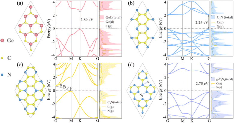 |
| | Fig. 1 Left panels of (a)–(d) show the crystal structures of GeC, C2N, C3N and g-C3N4 monolayers, respectively. The middle and right panels of (a)–(d) depict the band structures and projected density of states (PDOS) maps of the four monolayers. In the geometric structure diagrams, the Ge atoms are represented by pink color, C atoms are represented by yellow color, and N atoms are represented by blue color. | |
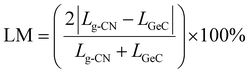
In order to construct high-performance photocatalysts, this study designs three types of g-CNs/GeC heterojunctions and then systematically explores their performance using first-principles calculations. In the process of heterojunction construction, lattice matching between the two monolayers is critical. It can be observed from Table 1 that the lattice constants of the three carbon–nitrogen monolayers significantly differ from that of the GeC monolayer. Therefore, it is necessary to conduct cell expansion for each monolayer to minimize the lattice mismatch ratio. The formula for calculating the lattice mismatch ratio can be written as follows:
| |  | (1) |
According to the above-mentioned formula, it can be calculated that when the unit cell of the C
2N monolayer (8.32 Å) is composite with the

expanded supercell of the GeC monolayer (8.64 Å), the lattice mismatch ratio is 2.55%. Similarly, when the

expanded C
3N monolayer (8.42 Å) is composite with the

expanded GeC monolayer (8.64 Å), and the 2 × 2 supercell of the g-C
3N
4 monolayer (9.56 Å) is composite with the 3 × 3 supercell of the GeC monolayer (9.78 Å), the lattice mismatch ratios are 3.69% and 2.39%. Under these settings, the carbon nitrogen monolayers and GeC monolayer can be perfectly matched to construct suitable heterojunctions, and the subsequent calculations are based on these three lattice configurations.
Table 1 Detailed parameters of the GeC, C2N, C3N and g-C3N4 monolayers for optimized-geometry lattice constant a (Å), bond length L (Å), bandgap for Eg-PBE (eV) and Eg-HSE 06 (eV)
| Monolayer |
a (Å) |
L (Å) |
E
g-PBE (eV) |
E
g-HSE 06 (eV) |
| GeC |
3.26 |
Ge–C 1.89 |
2.08 |
2.89 |
| C2N |
8.32 |
C–C 1.43/1.47 |
1.66 |
2.25 |
| C–N 1.34 |
| C3N |
4.86 |
C–C 1.40 |
0.39 |
0.91 |
| C–N 1.40 |
| g-C3N4 |
4.78 |
C–N1 146 |
1.57 |
2.75 |
| C–N2 1.37 |
With the goals of avoiding the randomness and finding the most stable lattice matching configurations, this work constructs six different stacking patterns for C2N/GeC, C3N/GeC, and g-C3N4/GeC heterojunctions (which are denoted as AB1–AB6). Subsequently, every configuration is comprehensively optimized. The fully optimized geometric configurations for three heterojunctions are shown in Fig. S1–S3 (ESI†), which demonstrate that all the patterns of the C2N/GeC and C3N/GeC heterojunctions remain almost undistorted. However, significant bending and deformation occur in the g-C3N4/GeC heterojunction due to the presence of dangling bonds in the g-C3N4 monolayer. Fortunately, there are no chemical bonds formed between the GeC layer and the g-C3N4 monolayer; therefore, the interaction forces between the two monolayers are purely physical forces. Then, it is observed that the interlayer distances (d) between the two layers in all configurations of three heterojunctions fall within the typical range of van der Waals forces (as shown in Table 2). Notably, the interlayer spacings of the g-C3N4/GeC heterojunction are significantly smaller than that of the other two heterojunctions, which indicate the stronger interfacial interactions between the g-C3N4 and GeC layers, thus bringing about the more compact contact between the individual monolayers.
Table 2
E
g-PBE (eV) and Eg-HSE 06 (eV), the work function Φ (eV), C11, C12 and C66 for the representative configurations of C2N/GeC, C3N/GeC and g-C3N4/GeC heterojunctions
| Structures |
E
g-PBE (eV) |
E
g-HSE06 (eV) |
Φ (eV) |
C
11
|
C
12
|
C
66
|
| C2N/GeC |
0.36 |
0.96 |
5.20 |
321.43 |
105.29 |
108.07 |
| C3N/GeC |
0.37 |
0.85 |
3.92 |
518.82 |
110.30 |
204.26 |
| g-C3N4/GeC |
1.35 |
2.08 |
5.17 |
286.70 |
59.94 |
113.38 |
The essential task after constructing heterojunctions is to assess the stability of these three heterojunctions, especially the g-C3N4/GeC heterojunction with noticeable deformations. First, the binding energy serves as the primary criterion for judging the stability of heterojunctions, and the formula for calculating the binding energy is as follows:
| | | Eb = Eg-CN/GeC − Eg-CN − EGeC | (2) |
where
Eg-Cn/GeC is the total energy for each of heterojunctions,
Eg-CN is the total energy for each of carbon nitrogen monolayers and
EGeV is the total energy for the GeC monolayer. As is well known, the stability of the structures is initially indicated by the negative values of binding energy, and the smaller binding energy suggests stronger interaction force. According to Table S1 (ESI
†), it can be revealed that all the patterns of the C
2N/GeC, C
3N/GeC, and g-C
3N
4/GeC heterojunctions are stable, and the most stable configurations of the three heterojunctions are AB6, AB5, and AB2, respectively, and the crystal structures of the three configurations are shown in
Fig. 2. Then the three configurations are selected as representatives for each heterojunction to conduct the following calculations and discussions.
 |
| | Fig. 2 Crystal structures of three representatives with (a) AB6 stacking of C2N/GeC, (b) AB5 stacking of C3N/GeC and (c) AB2 stacking of g-C3N4/GeC heterojunctions, which originated from the VESTA software package. In the geometric structure diagrams, the Ge atoms are represented by pink color, C atoms are represented by yellow color and N atoms are represented by blue color. | |
For the purpose of ensuring the theoretical and experimental research values of the three heterojunctions, the molecular dynamics58 and elastic constant calculations59 were performed to fully validate their stability performance. In the calculations of molecular dynamics, the 2 × 2 supercell structures are employed for each of the three heterojunctions to minimize temperature fluctuations. The simulations were carried out at a temperature of 300 K, and the structures were calculated up to 3.0 ps by 1.0 fs steps. Fig. 3 presents the top views of the geometric structures after heating as well as the fluctuations of free energy with respect to time during the heating processes. It can be observed that there is no geometric rearrangement or cleavage of chemical bonds in the three heated heterojunctions, and the fluctuations of free energy over time are relatively minimal, indicating that all three heterojunctions display good thermodynamic stability. Additionally, the elastic constant provides a measure to determine whether the three heterojunctions possess mechanical stability. When the calculated values of the elastic constant satisfy the conditions C11 > C12 and C66 = (C11 − C12)/2 > 0, the structures possess good mechanical stability. The results in Table 2 illustrate that all three heterojunctions perfectly meet the above-mentioned criteria, thus confirming their great mechanical stability performance. Overall, the stabilities of the three heterojunctions were verified, which provide a solid prerequisite for their broader potential applications.
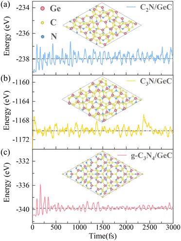 |
| | Fig. 3 Top views of 2 × 2 supercell structures and the fluctuations in free energy during a 300 K molecular dynamics simulation over a time scale of 3.0 ps are depicted for the (a) C2N/GeC, (b) C3N/GeC and (c) g-C3N4/GeC heterojunctions. | |
Electronic properties
The electronic properties of heterojunctions can serve as the preliminary criterion for determining whether the three heterojunctions have potential applicability for photocatalytic water splitting. Therefore, it is inevitable to systematically investigate the electronic characteristics of the three heterojunctions. Interlayer interactions between the two monolayers in the heterojunctions have an impact on electronic properties that can be assessed through the band structures and PDOS maps, as shown in the left and middle panels of Fig. 4(a)–(c). The obtained results indicate that the C2N/GeC heterojunction has an indirect bandgap of 0.36 eV/0.96 eV (PBE/HSE06), with the CBM predominantly originating from the C2N layer and the VBM is occupied by the GeC layer. It is intriguing that both the C2N monolayer and the GeC monolayer are direct bandgap semiconductors, whereas the C2N/GeC heterojunction exhibits the indirect bandgap. This trait can be attributed to the fact that the VBM of the GeC layer and the CBM of the C2N layer located at the high symmetry point K and G, respectively, and the C2N/GeC heterojunction preserve the band curve characteristics of the two individual layers, resulting in an indirect bandgap. Compared with the direct bandgap, the characteristics of indirect bandgap can productively suppress the recombination of electron–hole pairs, thereby prolonging the carrier lifetime. Similarly, the C3N/GeC heterojunction retains the indirect bandgap of the C3N monolayer and also shows an indirect bandgap. The CBM and VBM are located at the high symmetry points G and M, respectively, and both the CB and VB are occupied with the C3N layer. The bandgap of the C3N/GeC heterojunction is 0.37 eV/0.85 eV (PBE/HSE06), which is minimally different from the bandgap of the C3N monolayer and is also close to that of the C2N/GeC heterojunction. In contrast, the g-C3N4/GeC heterojunction displays a direct bandgap of 1.35 eV/2.08 eV (PBE/HSE06), with the CBM and VBM both located at the high symmetry point G in the Brillouin zone. Direct bandgap semiconductors keep the K point unchanged during electronic transition, so there is no need for the phonons to participate, thus making electronic transitions easier. Besides, the 2.08 eV bandgap of the g-C3N4/GeC heterojunction is very close to the ideal bandgap for photocatalytic water decomposition within the visible-light range. The CB and VB are dominated by the g-C3N4 and GeC layers, respectively, which is the same characteristic as the C2N/GeC heterojunction. Furthermore, the bandgaps of the three heterojunctions are smaller than the bandgaps of the constituent monolayers. The smaller bandgap enables electrons to be more easily excited from the VB to CB, which facilitates the transfer of electrons and provides evidence for the conclusion that the heterojunctions can stimulate superior performance; therefore, the C2N/GeC heterojunction may exhibit better performance than the g-C3N4/GeC heterojunction. This characteristic can also be reflected on other heterojunction systems such as GeC/SiC,60 AlN/BP61 and WTe2/InSe62 heterojunctions, thereby affirming the correctness of the calculations in this work.
 |
| | Fig. 4 Left and middle panels of (a)–(c) portray band structures and PDOS maps of the C2N/GeC, C3N/GeC and g-C3N4/GeC heterojunctions, and the side views of LUMO and HOMO are shown in the right panels. | |
Additionally, the right panels of Fig. 4(a)–(c) depict the HOMO and LUMO diagrams of the three heterojunctions. The conclusions highly conform to the conclusions of the band structure and PDOS plots. According to the electronic properties, it can be concluded that C3N/GeC is a type-I heterojunction. The fast recombination of electrons and holes in type-I heterojunctions makes them unsuitable to be efficient photocatalysts for water splitting. However, both C2N/GeC and g-C3N4/GeC heterojunctions exhibit the typical staggered type-II band alignment. In the type-II heterojunctions, the CB and VB are provided by different monolayers, which allow for the spatial separation of electron–hole pairs and hinder the recombination of carriers. Therefore, the C2N/GeC and g-C3N4/GeC heterojunctions hold great potentials in the field of photocatalysis.
Interfacial properties
The strong interactions between the interface of heterojunctions are accompanied by charge transfer. In order to gain a deeper understanding of the charge transfer at the interface and further judge the types of these three heterojunctions, the work function diagrams of each monolayer material, the 3D charge density differences, the planar-averaged charge density differences, the planar-averaged electrostatic potential diagrams, and the Bader charge analysis of the three heterojunctions were calculated and plotted in this part to visualize and quantitatively describe the charge transfer.
It is firmly believed that the work function (Φ) of each material is a prerequisite for determining the charge redistributions and forming the built-in electric fields.61,63 Therefore, the work function potentials of each monolayer material were calculated. The calculation formula of the work function is Φ = Evacuum − EF, where Evacuum and EF represent the vacuum and Fermi level. Fig. 5 shows the work function diagrams of the four monolayer materials, and it can be observed that the work function of the GeC monolayer is smaller than that of the C2N and g-C3N4 monolayers, respectively. Therefore, for the C2N/GeC and g-C3N4/GeC heterojunctions, the difference in work function between the two monolayers causes electrons to transfer from the GeC layer to the C2N and g-C3N4 layers until the Fermi levels align in equilibrium. As a result, positive charges accumulate on the GeC layer, while the C2N and g-C3N4 layers are negatively charged, respectively, and the space charge region is formed. Meanwhile, the charge interactions in the space charge region induce the electrostatic induction effect, leading to the formation of the built-in electric fields, which are directed from the GeC layer towards the C2N and g-C3N4 layers, respectively. Fig. 6(a) displays the schematic diagram that depicts the relationship between the band edge potentials and the standard hydrogen electrode of each monolayer and heterojunction. It can be seen from that when the heterojunctions are irradiated by visible-light, electrons are excited from the VB to CB, leading to significant electron accumulation in the CB and significant holes remaining in the VB. Under the action of the built-in electric fields, electrons in the GeC layer are repelled by the negative charges in the C2N and g-C3N4 layers, leading to an upward bending of the band edge in the GeC layer. Similarly, the band edges of the C2N and g-C3N4 layers are bent downward. The bending of the band edges creates the potential barriers at the interface of the heterojunctions, impeding the transfer of electrons from the CB of the GeC layer to the CB of the C2N and g-C3N4 layers. Likewise, the transfer of holes from the VB of the C2N and g-C3N4 layers to the VB of the GeC layer is also suppressed. More importantly, the bending of band edges only allow electrons at the CB of the C2N and g-C3N4 layers to migrate to the VB of the GeC layer, resulting in a large number of recombination between electrons gathered at the lower energy level of the CB and holes trapped at the higher energy level of the VB. Consequently, the redox reactions of photocatalytic water splitting will occur at the CB of the GeC layer with stronger reduction ability and the VB of the g-CN layer with stronger oxidation ability, respectively. The above-mentioned reaction mechanism is shown in Fig. 6(b).
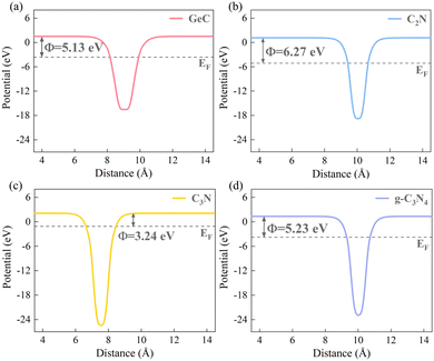 |
| | Fig. 5 Work function Φ of the (a) GeC, (b) C2N, (c) C3N and (d) g-C3N4 monolayers. The horizontal black dotted lines denote the Fermi level. | |
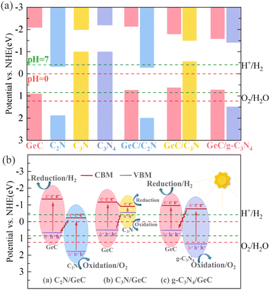 |
| | Fig. 6 (a) Calculated band-edge position of the four monolayers and the three heterojunctions with reference to the standard hydrogen electrode at pH = 0 and pH = 7, which are represented by red and green dashed lines. (b) Schematic diagrams of the charge transfer process of the three heterojunctions illuminated by visible light. | |
Surprisingly, it was found that the C2N/GeC and g-C3N4/GeC heterojunctions satisfy the reaction mechanism of the Z-scheme heterojunctions; therefore, we conclude that the C2N/GeC and g-C3N4/GeC heterojunctions are Z-scheme heterojunctions. Continuing on that note, due to the spatial separation of electron–hole pairs and the formation of energy barriers, Z-scheme heterojunctions significantly broaden the redox potential, isolating active electrons and holes,64 which can further suppress the recombination of electron–hole pairs, enabling the redox reactions to proceed at energy levels with stronger oxidation and reduction capabilities. Therefore, the Z-scheme heterojunctions are expected to shine brightly as the efficient and excellent photocatalysts with their superior oxidation and reduction performance. Additionally, the band edge potential distributions of the C3N/GeC heterojunction are also illustrated in Fig. 6(a). From the figure, we can observe that the CB and VB of the C3N layer are positioned within the bandgap width of the GeC layer, and the characteristic is satisfied by the nested alignment of type-I heterojunctions. When the C3N/GeC heterojunction is illuminated, electrons are elevated from the VB to the CB. Since the CB and VB of the C3N layer are nested in the bandgap width of the GeC layer, the electrons in the CB and the holes in the VB of the GeC layer are transferred and accumulated at the CB and VB of the C3N layer, respectively. Consequently, the electrons and holes cannot be spatially separated, limiting the application of the C3N/GeC heterojunction as a photocatalyst. Nonetheless, the highly efficient electron–hole pair recombination mechanism and the small bandgap of the C3N/GeC heterojunction make it still hold promise for application in optoelectronic devices.
Next, the 3D charge density difference, planar-averaged charge density difference, planar-averaged electrostatic potential, and Bader charge analysis were utilized to testify the charge transfer in the three heterojunctions. Fig. 7(a)–(c) present the 3D charge density difference diagrams for the three heterojunctions, which can graphically display the charge transfer between the interfaces of the heterojunctions, wherein the purple and red regions symbolize the charge depletion and accumulation. In the cases of the two Z-scheme heterojunctions (C2N/GeC and g-C3N4/GeC heterojunctions), charge depletion primarily occurs at the interface and near the surface of the GeC layer, while charge accumulation mainly takes place near the interface and the surface of the g-CN layer. The planar-averaged charge density difference maps are portrayed in Fig. 7(d), which provides a quantitative representation of the charge transfer between the three heterojunction interfaces. The charge accumulation is indicated by positive values, while charge depletion is represented by negative values. The results of the charge transfer trends are aligned with the 3D charge density difference maps. The charge depletion occurs near the GeC layer and at the interfaces, with maximum depletion values of 3.12 × 10⁻² e Å−1 and 5.13 × 10⁻² e Å−1, respectively. The charge accumulation takes place near the C2N and g-C3N4 layers, respectively, with maximum accumulation values of −2.36 × 10⁻² e Å−1 and −7.18 × 10⁻² e Å −1respectively. However, in the C3N/GeC heterojunction, charge depletion and accumulation predominantly occur near the C3N and GeC layers, with maximum depletion and accumulation values of −1.06 × 10⁻¹ e Å−1 and 5.25 × 10⁻² e Å−1 respectively. Notably, the charge depletion and accumulation in the C3N/GeC heterojunction present distinct layering phenomena. In short, it can be observed that the maximum values of charge accumulation and depletion occur in the C3N/GeC heterojunction, and the minimum values appeared in the C2N/GeC heterojunction. The amount of charge transfer is closely related to the potential difference, and hence, we speculate that the potential difference between the two components of the C3N/GeC heterojunction is the largest among the three heterojunctions, and the potential difference in the C2N/GeC heterojunction is the smallest. Then, the planar-averaged electrostatic potential plots of the three heterojunctions were calculated to test this hypothesis, which are shown in Fig. 7(e). There are potential differences of 0.89 eV, 9.14 eV, and 2.48 eV between the two components in the C2N/GeC, C3N/GeC and g-C3N4/GeC heterojunctions, respectively, which is consistent with our previous conjecture. The potential difference between different components not only proves the charge transfer between interfaces, but also verifies the existence of built-in electric fields. Simultaneously, Table 3 presents the Bader charge analysis results for the three heterojunctions. In the Z-scheme heterojunctions of C2N/GeC and g-C3N4/GeC, it is observed that the Ge atoms in the GeC layer and C atoms in the g-CN layer lose electrons, while the C atoms in the GeC layer and N atoms in the g-CNs layer gain electrons. Regarding the component level of each layer, the GeC layer transfers 0.1387e and 0.1124e to the C2N and g-C3N4 layers, respectively, which is in accordance with the aforementioned calculations. Conversely, for the C3N/GeC heterojunction, the electron transfer occurs in the opposite direction with the two Z-scheme heterojunctions. In summary, the Bader charge analysis results support the conclusion of interfacial charge transfer and further confirm the types of the three heterojunctions.
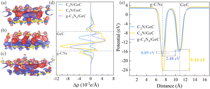 |
| | Fig. 7 (a)–(c) Three-dimensional charge density difference among the C2N/GeC, C3N/GeC and g-C3N4/GeC heterojunctions, where the charge accumulation and consumption are represented by red and purple regions, respectively. (d) Profile distributions of planar-averaged charge density difference along the vertical direction for the three heterojunctions. The charge accumulation and charge loss are denoted by positive and negative values. (e) Planar-averaged electrostatic potentials along the vertical direction of the three heterojunctions. | |
Table 3 Bader charge analysis of C2N/GeC, C3N/GeC and g-C3N4/GeC heterojunctions. Positive and negative values represent the gain and loss of electrons, respectively
| Structures |
Charge/atom |
Charge/atom |
Charge/layer |
| C2N/GeC |
Ge −1.3394 |
C 1.3195 |
GeC −0.1387 |
|
|
C −0.5206 |
N 1.0644 |
C2N 0.1387 |
| C3N/GeC |
Ge −1.3085 |
C 1.3148 |
GeC 0.0437 |
|
|
C −0.4025 |
N 1.2003 |
C3N −0.0437 |
| g-C3N4/GeC |
Ge −1.3864 |
C 1.3738 |
GeC −0.1124 |
|
|
C −1.4309 |
N 1.0802 |
g-C3N4 0.1124 |
Carrier mobility
During the process of exploring the charge transfer, carrier mobility plays a crucial role. Carrier mobility is an important parameter for measuring the conductivity of semiconductors, which is utilized to reveal the motion speed of internal electrons and holes under the action of a unit electric field. It can be divided into electron mobility and hole mobility. The value of carrier mobility determines the amount of photogenerated electrons and holes participating in the photocatalytic water splitting process, thereby affecting the quantum efficiency of the entire photocatalytic reaction. Therefore, it is an essential factor that influences the activity of photocatalysts. The higher the carrier mobility, the better the performance of the photocatalyst will be. As stated in the previous section regarding stability properties, the effective mass is a metric for assessing the mechanical stability of heterojunctions. Additionally, the effective mass also determines the electron–hole pair mobility, thereby influencing the carrier mobility values. Generally, larger effective mass correspond to slower carrier mobility. Consequently, the effective mass approximation and deformation potential theory were employed to investigate the carrier mobility of the three heterojunctions in this study, which is described by eqn (3):65–67| |  | (3) |
| |  | (4) |
| |  | (5) |
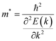
where e is the amount of electron charge, ħ is the reduced Planck constant, kB is the Boltzmann constant, and T is the temperature (set to 298.15 K in this work). M* is the effective mass for  and
and  , which can be obtained using formula (5). E(k) and k mean the energy and momentum, respectively. The effective mass of electrons
  and the effective mass of holes
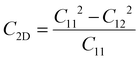
  can be obtained by performing a quadratic fit to the band curvatures around the CBM and VBM of the heterojunctions. C2D denotes the elastic modulus of the materials along the transmission direction, which can be calculated by elastic constants, and the relationship between the elastic modulus and the elastic constants is described using formula (6). In addition, E1 is the deformation potential energy constant (DP) of the electrons gathered at the CBM and the holes accumulated at the VBM along the transmission direction, which denotes the linear fitting of band edge changes induced by applying biaxial strains. Fig. 8(a) presents the linearly fitted band edge curves of the CBM (VBM) potentials of the heterojunctions under biaxial strains ranging from −1.5% to +1.5% for the three heterojunctions. The slopes of these curves correspond to the values of the deformation potential constants for electrons (E1e) and holes (E1h). It can be observed that the DP curves are well fitted within the error range. Subsequently, the electron and hole mobility of the three heterojunctions were computed, and the detailed data of carrier mobility are presented in Table 4. It can be observed that both the C2N/GeC and g-C3N4/GeC heterojunctions exhibit small values of
  and large values of
  . Besides, they have similar values of C2D and a relatively small difference of E1e and E1h. Under the circumstances, the carrier mobility was mainly determined by
  and
and  . As a result, both C2N/GeC and g-C3N4/GeC heterojunctions demonstrate high electron mobility and low hole mobility. The μe/μh value of the C2N/GeC heterojunction is 1.79 × 10³/0.57 × 103 cm2 V−1 s−1, and the μe/μh value of the g-C3N4/GeC heterojunction is 2.29 × 10³/0.11 × 103 cm2 V−1 s−1, respectively. Obviously, the carrier mobility of the g-C3N4/GeC heterojunction is higher than that of the C2N/GeC heterojunction. Therefore, the g-C3N4/GeC heterojunction shows a better photocatalytic performance than that of the C2N/GeC heterojunction. This is mainly due to the direct bandgap of the g-C3N4/GeC heterojunction, which eliminates the need for phonon participation when electrons are excited and is more conducive to carrier transition. The excellent carrier mobility of C2N/GeC and g-C3N4/GeC heterojunctions is comparable to many other systems such as PtSe2/GaN,68 InTe/C2N69 and MoSSe/GeC70 heterojunctions. The large carrier mobility means fast migration of photogenerated electrons and holes, enabling carriers to quickly reach the reaction sites and enhancing the photocatalytic activities. Furthermore, there are significant differences in the values of μe and μh in both the Z-scheme heterojunctions, which favor the spatial separation of electron–hole pairs and hinder the recombination of photogenerated carriers. In contrast, although the C3N/GeC heterojunction is not suitable for a photocatalyst, the smaller effective mass gives it excellent electron and hole mobility, The high carrier mobility enables the fast migration of electrons and holes, which is advantageous for its application in optoelectronic fields.
 |
| | Fig. 8 (a) After the biaxial strain in the range from −1.5% to 1.5% is applied to the three heterojunctions, the deformation potential constant is obtained by linear fitting of the energy level band edge relative to the vacuum levels. (b) Optical absorption spectra in the visible-light range of the four monolayers and three heterojunctions, where the absorption curves of the four monolayers are represented by dashed lines, and three heterojunctions are given by solid lines. | |
Table 4 Elastic constants (C11 and C12) and elastic modulus (C2D), effective mass ( and
and  ), deformation potential constant (E1e and E1h) and carrier mobility (μe and μh) of the C2N/GeC, C3N/GeC and g-C3N4/GeC heterojunctions
| System |
C
11
|
C
12
|
C
2D
|
Carrier type |

|
E
1e/E1h |
μ
e/μh (cm2 V−1 s−1) |
| C2N/GeC |
321.43 |
105.29 |
286.94 |
Electron |
−0.46 |
−3.28 |
1.79 × 10³ |
| Hole |
−1.12 |
−2.39 |
0.57 × 10³ |
| C3N/GeC |
518.82 |
110.30 |
495.37 |
Electron |
−0.26 |
−5.92 |
3.00 × 10³ |
| Hole |
−0.29 |
−6.54 |
1.95 × 10³ |
| g-C3N4/GeC |
286.70 |
59.94 |
274.17 |
Electron |
−0.48 |
−2.70 |
2.29 × 10³ |
| Hole |
1.57 |
−3.78 |
0.11 × 10³ |
Photocatalytic properties
Based on the previous calculation results of the electronic properties, interfacial properties and carrier mobility, it can be inferred that C2N/GeC and g-C3N4/GeC heterojunctions exhibit Z-scheme band alignment and demonstrate great carrier mobility, making them highly promising candidates for photocatalytic water splitting. Nonetheless, only when the band edge potentials of the heterojunctions simultaneously straddle the reduction and oxidation potentials of water decomposition, with the reduction potential higher than that of H+/H2 and the oxidation potential lower than that of O2/H2O, can the heterojunctions effectively decompose water into hydrogen and oxygen. The standard reduction and oxidation potentials of H+/H2 and O2/H2O both exhibit an upward trend with the increase in pH value. The formulas for determining the water reduction and oxidation potentials with reference to the vacuum energy under various pH conditions are as follows:71| | | EH+/H2 = −4.44 eV + pH × 0.059 eV | (6) |
| | | EO2/H2O = −5.67 eV + pH × 0.059 eV | (7) |
According to the reaction mechanism diagrams of C2N/GeC and g-C3N4/GeC heterojunctions shown in Fig. 6, it can be observed that although the VB of two Z-scheme heterojunctions does not span the oxidation potential for water splitting, the unique charge transfer pathway retains the electrons and holes with stronger reduction and oxidation capability. As a result, the reduction and oxidation reactions take place at the CB of the GeC layer and the VB of the g-CN layer, respectively, which can perfectly straddle the redox potentials for water decomposition within the pH range of 0–7. Therefore, the two Z-scheme heterojunctions designed in this work demonstrate great potential for application in the field of photocatalysis for hydrogen production.
It is public knowledge that the calculations of the hydrogen evolution reaction (HER) and oxygen evolution reaction (OER) can directly reflect the hydrogen and oxygen evolution capabilities of heterojunctions, which play vital roles in water splitting. If the intermediate reactants of the HER and OER fail to promptly adsorb onto the surface of the heterojunctions, the reaction rate and efficiency of the heterojunctions will be repressed. Therefore, the Gibbs free energy of the intermediate reactants during the HER and OER of C2N/GeC and g-C3N4/GeC heterojunctions was calculated to investigate their reactivity.
The HER catalytic performance was evaluated by calculating the Gibbs free energy (ΔG) for the hydrogen atom adsorbed on the heterojunction surface. The equations of state for the HER process can be written as follows:
| |  | (9) |
wherein * represents the active site on the heterojunction surface, H* represents a hydrogen atom adsorbed on the heterojunction surface, which is also the intermediate of the HER process, and there is only one intermediate state in the HER process. The formula for calculating the Δ
G value of the intermediate state is as follows:
72| | | ΔG = ΔEads + ΔEZPE − TΔS | (10) |
where Δ
Eads is the adsorption energy, Δ
EZPE is the zero-point energy (ZPE), Δ
S is the change of entropy, and the value of
T is 298.15 K. Δ
G is the state coefficient of the system that reflects the efficiency of the HER. The |Δ
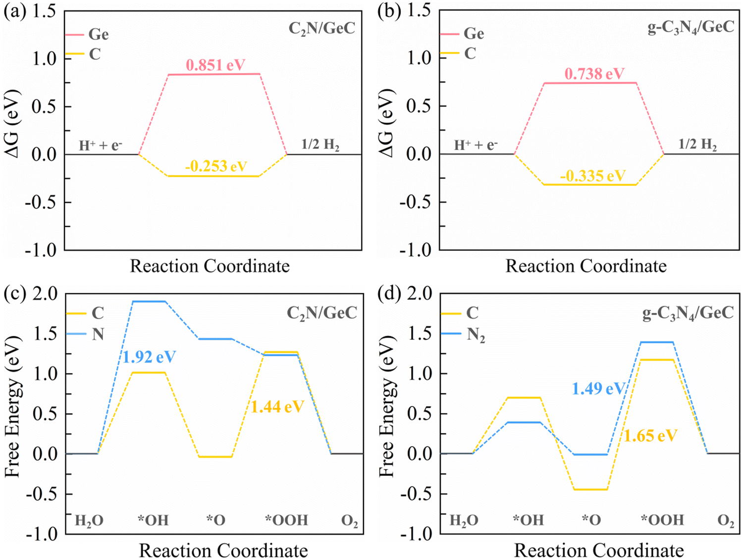
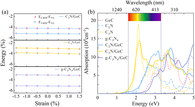
G| value of a high-efficiency catalyst should be close to 0 eV; the closer the value to 0 eV, the faster the HER rate will be. As the HER occurs on the electrode which provides electrons, the H atoms adsorbed on the GeC layer are considered. Both Ge and C atoms in the GeC layer are active sites for bonding unsaturated, therefore the two scenarios are considered.
Fig. 9(a) and (b) present the Gibbs free energy diagrams of the HER occurring on C
2N/GeC and g-C
3N
4/GeC heterojunctions, respectively. In comparison to the Ge atom adsorption site, the hydrogen atom is more likely to be adsorbed on the C atom, and the Δ
G values on the C atom site for C
2N/GeC and g-C
3N
4/GeC heterojunctions are −0.253 eV and −0.335 eV, respectively. The values both are close to zero, which illustrate that both C
2N/GeC and g-C
3N
4/GeC heterojunctions possess good HER performance. Moreover, the |Δ
G| value for the C
2N/GeC heterojunction is closer to zero, indicating a faster HER rate than that of the g-C
3N
4/GeC heterojunction.
 |
| | Fig. 9 For the C2N/GeC and g-C3N4/GeC heterojunctions, (a) and (b) Gibbs free energy diagrams of the HER occurring on Ge and C atoms in the GeC layer. (c) and (d) Gibbs free energy change diagrams of the OER on the surface of C2N and g-C3N4 layers for C and N (N2) atoms. | |
In order to calculate the OER performance of the C2N/GeC and g-C3N4/GeC heterojunctions and understand the underlying photocatalytic mechanism, this work investigates the OER on the two Z-scheme heterojunctions. The OER can be divided into four steps under conditions of pH = 0 and T = 298.15 K, and the reaction state equations can be written as follows:73
| | | * + H2O(l) → OH* + H+ + e− | (11) |
| | | O* + H2O(l) → OOH* + H+ + e− | (13) |
| | | OOH* → * + O2(g) + H+ + e− | (14) |
where * represents the active site that the intermediate reactants can be adsorbed on the heterojunction surface and H
2O(1) represents liquid water molecules. OH*, O* and OOH* represent the intermediate adsorption states in the OER, and O
2(g) represents the generated gaseous O
2 molecule. The formula for calculating the Δ
G value of each intermediate reactant in the OER is as follows:
| | | ΔG = ΔEads + ΔEZPE − TΔS + ΔGpH + ΔGU | (15) |
In the equation, Δ
Eads is the adsorption energy and Δ
EZPE is the zero-point energy (ZPE) for each step of the reaction process, and Δ
S is the change in entropy. Δ
GpH is the correction of H
+ free energy by the concentration dependence of entropy to account for the influence of pH, Δ
GpH =
kBT![[thin space (1/6-em)]](https://www.rsc.org/images/entities/char_2009.gif)
ln × pH. Δ
GU is defined as −
eU, where
U represents the electrode potential. An ideal catalyst has an energy difference of 1.23 eV between two adjacent intermediate states, which means that the OER will occur spontaneously without any additional drive when the energy difference between the VB and CB (where the oxidation and reduction reactions occur) in the heterojunction is greater than 1.23 eV. However, in practical operation, the OER requires overcoming a considerable additional overpotential to ensure that the reaction proceeds, which can be driven by external electric fields or solar energy. The overpotential in the OER depends on the step with the largest Δ
G among the four reaction steps, which is the rate-determining step that determines the reaction rate. The theoretical overpotential for the OER was calculated as follows:
| |  | (17) |
The OER of the C
2N/GeC heterojunction occurs in the C
2N layer, and the C and N atoms in the C
2N layer are bonding unsaturated. Therefore, the two situations are considered to perform OERs.
Fig. 9(c) illustrates the free energy change during the OER process at the C
2N/GeC heterojunction. The results indicate that the energy requirements of C and N atoms for each step are obviously different. Specifically, the formations of O* and OH* intermediates at C atom sites are endothermic processes, while the second and fourth steps are exothermic processes. In addition, the rate-determining step is the formation of OOH*. On the contrary, for the OER at N atom sites, the first step is the rate-determining step, followed by three exothermic steps. Notably, the overpotential for the rate-determining step at C atom sites (1.44 eV) is much lower than that at the N atom sites (1.92 eV). Therefore, the C atoms re more favorable for undergoing the OER. With respect to the g-C
3N
4/GeC heterojunction, the OER process occurs in the g-C
3N
4 layer, where the C and N
2 atoms are bonding unsaturated. Therefore, there are also two situations considered to perform OERs.
Fig. 9(d) presents the free energy variation diagram of the OER on unsaturated C and N
2 atoms at the g-C
3N
4/GeC heterojunction. Both the free energy variation curves show similar trends with the OER that occurs on C atoms at the C
2N/GeC heterojunction, and the overpotential of N
2 atoms (1.49 eV) at the g-C
3N
4/GeC heterojunction is slightly lower than that of C atoms (1.65 eV), indicating that the OER is more favorable to occur at N
2 atom sites. In summary, the OERs are more likely to occur at C atom sites in the C
2N/GeC heterojunction and at N
2 atom sites in the g-C
3N
4/GeC heterojunction, with the overpotential values of 1.44 eV and 1.49 eV, respectively. The overpotentials for the two Z-scheme heterojunctions are relatively close, which suggest comparable OER performance, and the values of overpotential are smaller than that of other systems such as C
6N
6/C
2N,
74 PtSe
2/Sb
2S
3,
75 and PtSe
2/SnS
276 heterojunctions. Therefore, the C
2N/GeC and g-C
3N
4/GeC heterojunctions both demonstrate promising OER activities and can serve as viable photocatalysts for oxidation.
Optical properties
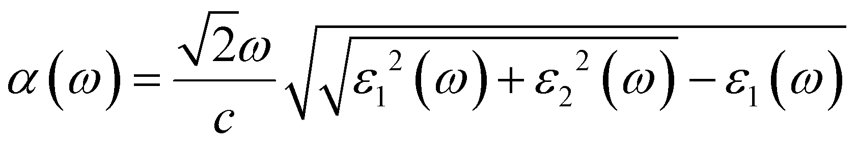
Additionally, the optical properties, especially the absorption abilities in the visible-light range, are closely related to the photocatalytic activities. As a photocatalyst for water splitting, possessing a broad and strong visible-light absorption capability is an important criterion for evaluating the photocatalyst efficiency. The light absorption capability is assessed by the absorption coefficient (α(ω)), which can be calculated using the following formula:77| | 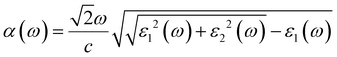 | (18) |
where ω and c represent the angular frequency and the speed of light in vacuum. ε1(ω) and ε2(ω) respectively denote the real and imaginary parts of the dielectric constant, and the ε2(ω) parameter also reflect the light absorption characteristics of the photocatalysts. In this work, the optical absorption properties of four monolayers and three heterojunctions were calculated using the HSE06 functional method. The optical absorption spectra are shown in Fig. 8(b), where the absorption curves of the four monolayers are represented by dashed lines, and three heterojunctions are represented by solid lines. It is noticeable that the peak value of the absorption coefficient for the C2N monolayer (8.17 × 104 cm−1) within the visible-light range is higher than that of the GeC monolayer (6.43 × 104 cm−1), and the visible-light range of the C2N monolayer is wider than that of the GeC monolayer; therefore, the C2N monolayer shows a stronger light absorption capability compared to the GeC monolayer. Fortunately, the C2N/GeC heterojunction exhibits a significantly higher absorption coefficient peak of 1.18 × 105 cm−1, which surpasses both individual monolayers and implies a remarkable enhancement in the light absorption intensity. Furthermore, the C2N/GeC heterojunction demonstrates the wider absorption range, with its absorption edge extending from the visible-light region to the infrared light range, which improves the light absorption performance. Besides, the C3N monolayer holds the strongest light absorption ability and the broadest absorption range among the four monolayers, there are three absorption coefficient peaks within the visible-light range, and the peak value can reach 1.89 × 105 cm−1. In comparison, the absorption peak of the C3N/GeC heterojunction exhibits slight attenuation within the visible-light range, yet the peak value still reached 1.45 × 105 cm−1, and there are five peaks appearing within the visible-light range, so the C3N/GeC heterojunction still indicates great absorption capacity. Additionally, the absorption range of the C3N/GeC heterojunction experiences a slight redshift compared to the C3N monolayer and combines the strong ultraviolet light absorption characteristic of the GeC monolayer, resulting in a significant improvement in the light absorption ability within the ultraviolet light range (compared to the C3N monolayer). These manifestations provide the C3N/GeC heterojunction with much possibility for remarkable performance in the field of optoelectronic devices. In contrast to the C3N monolayer, the g-C3N4 monolayer shows a poor light absorption capacity in the visible range, only being able to absorb a small portion of short-wavelength visible-light. Surprisingly, the g-C3N4/GeC heterojunction also combines the visible-light absorption capability of GeC monolayer, thereby enhancing the light absorption range of the g-C3N4 layer; therefore, the absorption edge shows a noticeable redshift relative to the g-C3N4 layer. Although the visible-light range of the heterojunction is slightly narrower than that of the GeC monolayer, its visible-light absorption coefficient peak (6.83 × 104 cm−1) in the wavelength range of 380–400 nm is higher than that of the GeC monolayer (6.43 × 104 cm−1), which is comparable to the ZnO/GaN system. Overall, the three heterojunctions not only preserve the original optical characteristics of the two individual monolayers but also integrate the optical advantages of both. The charge transfer between the heterojunctions, interlayer coupling, and hybridization overlap of electronic states between the two monolayers allow for the excitation of electrons, which significantly increase the light absorption intensity of the heterojunction in the visible and ultraviolet range, thereby improving the photocatalytic efficiency of the three heterojunctions. Consequently, it is expected to be efficient photocatalysts and solar energy conversion materials for the three heterojunctions.
Conclusions
This work employed first-principles calculations to conduct an in-depth investigation on the geometric structure, stability, electronic properties, interfacial characteristics, carrier mobility, photocatalytic properties and optical properties of the C2N/GeC, C3N/GeC, and g-C3N4/GeC heterojunctions, which were constructed by combining the C2N, C3N and g-C3N4 monolayers with the GeC monolayer, respectively. The interlayer interactions between the monolayer components are dominated by van der Waals forces, and all the three heterojunctions possess favorable thermodynamic and mechanical stabilities. The C2N/GeC and C3N/GeC heterojunctions possess relatively small bandgaps of 0.96 eV and 0.85 eV, which are advantageous for promoting the migration of photogenerated carriers. The g-C3N4/GeC heterojunction exhibits a larger direct bandgap (2.08 eV), which is close to the optimal bandgap for water splitting. The results of the optical absorption coefficients of the three heterojunctions are significantly increased in the visible and ultraviolet range, and accompanied by the redshift of the absorption edge, which enhances the solar utilization efficiency, thus indicating that the three heterojunctions are excellent visible-light photocatalysts. Moreover, the staggered band alignment of the C2N/GeC and g-C3N4/GeC heterojunctions enables effective carrier separation and powerfully suppresses the recombination of electron–hole pairs. Simultaneously, the difference in work functions and charge transfer between the monolayers form the built-in electric field directed from the GeC layer towards the g-CNs layer. The 3D charge density difference and Bader charge analysis further confirm the direction of charge transfer. Surprisingly, the built-in electric field enables the C2N/GeC and g-C3N4/GeC systems to comply with the reaction mechanism of Z-scheme heterojunctions, the unique charge transfer pathways that can further restrain the recombination of photogenerated electron–hole pairs and prolonging the carriers lifetime. Strikingly, the remarkable carrier mobility of the two Z-scheme heterojunctions implies the rapid migration of photogenerated electrons and holes, enabling the efficient charge transfer. Surprisingly, the two Z-scheme heterojunctions demonstrate suitable band edge potentials, enabling them to perfectly cross the redox potentials for water splitting in the pH range of 0–7. Additionally, the calculation results of Gibbs free energy indicate that both the Z-scheme heterojunctions are more likely to perform the HER at the C atoms of GeC layer, with |ΔG| values of −0.253 eV and −0.335 eV, respectively, which suggest rapid HER kinetics and good activity. Moreover, the C2N/GeC heterojunction exhibits a faster efficiency for HERs than that of the g-C3N4/GeC heterojunction. Meanwhile, the OER calculation results indicate that the C atoms in the C2N layer of the C2N/GeC heterojunction and the unsaturated N2 atoms in the g-C3N4 layer of the g-C3N4/GeC heterojunction are more favorable for the OER, with low overpotentials of 1.44 eV and 1.49 eV. Therefore, the C2N/GeC and g-C3N4/GeC heterojunctions both demonstrate promising OER activities and can serve as viable photocatalysts for oxidation production. Due to the very similar overpotential sizes required for the two Z-scheme heterojunctions, their oxygen evolution performances are comparable. In addition, although the C3N/GeC heterojunction is recognized as the traditional type-I heterojunction and cannot be utilized as a photocatalyst, the outstanding charge carrier mobility and optical performance make it promising for optoelectronic devices. To briefly summarize, this study has successfully designed two high-performance Z-scheme heterojunctions, namely, C2N/GeC and g-C3N4/GeC heterojunctions, which feature remarkable photocatalytic hydrogen and oxygen evolution abilities and exhibit broad application prospects as efficient photocatalysts for water splitting, and the photocatalytic performance of C2N/GeC heterojunction is superior to that of the g-C3N4/GeC heterojunction. These calculations in the work provide theoretical guidance and data support for the experimental preparation of efficient and feasible photocatalysts for water splitting hydrogen production.
Author contributions
Ying Zhang: data curation, formal analysis, writing – original draft, visualization. Hang Liu: writing – review & editing, supervision. Bo Zhang: methodology. Jingyao Shao: conceptualization, project administration. Zhiqiang Xu: validation. Yun Chao: validation. Ling-Ling Wang: project administration. Liang Xu: conceptualization, investigation, writing – review & editing, visualization, supervision, resources, project administration.
Conflicts of interest
There are no conflicts to declare.
Acknowledgements
This work was financially supported by the National Nature Science Foundation of China (Grant No. 52263031, 11764018), the Jiangxi Provincial Natural Science Foundation (Grant No. 20212BAB201013, 20202ACBL211004), the Science and Technology Research Project of Jiangxi Education Department (Grant No. GJJ210806), and the Science and Technology planning Project of Ganzhou City.
Notes and references
- S. H. Guo, X. H. Li, J. Li and B. Q. Wei, Nat. Commun., 2021, 12, 10 CrossRef PubMed.
- I. Shahid, S. Ahmad, N. Shehzad, S. Yao, C. V. Nguyen, L. Zhang and Z. Zhou, Appl. Surf. Sci., 2020, 523, 146483 CrossRef CAS.
- S. Jiang, Y. Liu and J. Xu, Mater. Adv., 2021, 2, 1190–1203 RSC.
- A. Fujishima and K. Honda, Nature, 1972, 238, 37–38 CrossRef CAS PubMed.
- S. Lin, H. Ren, Z. Wu, L. Sun, X. G. Zhang, Y. M. Lin, K. H. L. Zhang, C. J. Lin, Z. Q. Tian and J. F. Li, J. Energy Chem., 2021, 59, 721–729 CrossRef CAS.
- J. Zeng, L. Xu, X. Luo, T. Chen, S.-H. Tang, X. Huang and L.-L. Wang, Tungsten, 2022, 4, 52–59 CrossRef.
- C. T. Hou, H. Y. Liu and Y. J. Li, RSC Adv., 2021, 11, 14957–14969 RSC.
- W. Zhao, X. Y. Tu, X. M. Wang, B. L. Dai, L. L. Zhang, J. M. Xu, Y. Feng, N. Sheng and F. X. Zhu, Chem. Eng. J., 2019, 361, 1173–1181 CrossRef.
- K. S. Novoselov, A. K. Geim, S. V. Morozov, D.-E. Jiang, Y. Zhang, S. V. Dubonos, I. V. Grigorieva and A. A. Firsov, Science, 2004, 306, 666–669 CrossRef CAS PubMed.
- J. Xiao, M. Zhao, Y. Wang and X. Zhang, Nano Photonics, 2017, 6, 1309–1328 CAS.
- S. Tongay, J. Suh, C. Ataca, W. Fan, A. Luce, J. S. Kang, J. Liu, C. Ko, R. Raghunathanan and J. Zhou, Sci. Rep., 2013, 3, 2657 CrossRef PubMed.
- Y. Wang, Z. Ding, N. Arif, W.-C. Jiang and Y.-J. Zeng, Mater. Adv., 2022, 3, 3389–3417 RSC.
- X. Huang, L. Xu, H. Li, S. Tang, Z. Ma, J. Zeng, F. Xiong, Z. Li and L.-L. Wang, Appl. Surf. Sci., 2021, 570, 151207 CrossRef CAS.
- L. Xu, X. Huang, S. Xiong, Z. Wang, B. Peng, Z. Ma, J. Zeng, H. Li, S. Tang and Z. Li, Int. J. Hydrogen Energy, 2021, 46, 25060–25069 CrossRef CAS.
- S. H. Tang, L. Xu, K. J. Dong, Q. C. Wang, J. Zeng, X. Huang, H. T. Li, L. B. Xia and L. L. Wang, Appl. Surf. Sci., 2023, 615, 156357 CrossRef CAS.
- F. Opoku, O. Akoto, E. E. Kwaansa-Ansah, N. K. Asare-Donkor and A. A. Adimado, Mater. Adv., 2023, 4, 1949–1963 RSC.
- S. Han, X. Wei, Y. Huang, J. Zhang and J. Yang, Appl. Surf. Sci., 2022, 579, 152233 CrossRef CAS.
- H. Lin, R. Jin, S. Zhu and Y. Huang, Appl. Surf. Sci., 2020, 505, 144518 CrossRef CAS.
- W. Quan, J. Y. Bao, X. J. Meng, Y. Q. Ning, Y. A. Cui, X. Y. Hu, S. S. Yu and H. W. Tian, J. Alloys Compd., 2023, 946, 11 CrossRef.
- M. Du, Y. Sun, J. Zhao, H. Hu, L. Sun and Y. Li, Chin. Chem. Lett., 2023, 34, 108269 CrossRef CAS.
- E. Cerrato and M. C. Paganini, Mater. Adv., 2020, 1, 2357–2367 RSC.
- J. Tao, L. Xu, C. Li, S. Xiong, Z. Xu, J. Shao, L. Cao, Y. Zhang, K. Dong and L.-L. Wang, Phys. Chem. Chem. Phys., 2023, 25, 30924–30933 RSC.
- M. Mukherjee, R. Jana and A. Datta, Phys. Chem. Chem. Phys., 2021, 23, 3925–3933 RSC.
- Y.-J. Yuan, P. Wang, Z. Li, Y. Wu, W. Bai, Y. Su, J. Guan, S. Wu, J. Zhong and Z.-T. Yu, Appl. Catal., B, 2019, 242, 1–8 CrossRef CAS.
- A. Saraiva-Souza, M. Smeu, J. G. da Silva, E. C. Girao and H. Guo, J. Mater. Chem. C, 2017, 5, 11856–11866 RSC.
- Z. Ma, L. Xu, K. Dong, T. Chen, S. Xiong, B. Peng, J. Zeng, S. Tang, H. Li and X. Huang, Int. J. Hydrogen Energy, 2022, 47, 7202–7213 CrossRef CAS.
- X. Wang, R. Quhe, W. Cui, Y. Zhi, Y. Huang, Y. An, X. Dai, Y. Tang, W. Chen and Z. Wu, Carbon, 2018, 129, 738–744 CrossRef CAS.
- G. Zhao, W. Ma, X. Wang, Y. Xing, S. Hao and X. Xu, Adv. Powder Mater., 2022, 1, 100008 CrossRef.
- W. Wei, S. Yang, G. Wang, T. Zhang, W. Pan, Z. Cai, Y. Yang, L. Zheng, P. He and L. Wang, Nat. Electron., 2021, 4, 486–494 CrossRef CAS.
- X. Gao, Y. Shen, Y. Ma, S. Wu and Z. Zhou, Appl. Surf. Sci., 2019, 479, 1098–1104 CrossRef CAS.
- L. Gao, B. Zhou, J. Zhang, K. Jiang, L. Shang, Z. Hu and J. Chu, Solid State Sci., 2021, 122, 106771 CrossRef CAS.
- A. Bafekry, C. Stampfl and M. Ghergherehchi, Nanotechnology, 2020, 31, 295202 CrossRef CAS PubMed.
- X. Wang, K. Maeda, A. Thomas, K. Takanabe, G. Xin, J. M. Carlsson, K. Domen and M. Antonietti, Nat. Mater., 2009, 8, 76–80 CrossRef CAS PubMed.
- H. Tian, M. Liu and W. Zheng, Appl. Catal., B, 2018, 225, 468–476 CrossRef CAS.
- W. Zhang, Y. Ma, X. Zhu, S. Liu, T. An, J. Bao, X. Hu and H. Tian, J. Alloys Compd., 2021, 864, 158914 CrossRef CAS.
- K. Ren, W. Tang, M. Sun, Y. Cai, Y. Cheng and G. Zhang, Nanoscale, 2020, 12, 17281–17289 RSC.
- S. Feng, F. Guo, C. Yuan, Z. Wang, F. Miao and H. Zhang, Mater. Adv., 2022, 3, 9063–9070 RSC.
- R. Kumar, D. Das and A. K. Singh, J. Catal., 2018, 359, 143–150 CrossRef CAS.
- Y.-L. Liu, Y. Shi and C.-L. Yang, Appl. Surf. Sci., 2021, 545, 148952 CrossRef CAS.
- H. Li, L. Xu, X. Huang, J. Ou-Yang, M. Chen, Y. Zhang, S. Tang, K. Dong and L.-L. Wang, Int. J. Hydrogen Energy, 2023, 48, 2186–2199 CrossRef CAS.
- Y. Q. Kong, H. G. Sun, X. Zhao, B. Y. Gao and W. L. Fan, Appl. Catal., A, 2015, 505, 447–455 CrossRef CAS.
- Y. Jia, M. L. Mei, X. X. Xu and L. S. Wang, Solid State Sci., 2016, 56, 45–53 CrossRef CAS.
- M. A. Raza, F. Li, M. Que, L. Zhu and X. Chen, Mater. Adv., 2021, 2, 7187–7209 RSC.
- X. Zhao, Q. Liu, X. Li, H. Ji and Z. Shen, Chin. Chem. Lett, 2023, 34, 108306 CrossRef CAS.
- R. Yan, A. Zada, L. Sun, Z. Li, Z. Mu, S. Chen, F. Yang, J. Sun, L.-L. Bai, Y. Qu and L.-Q. Jing, Rare Met., 2022, 41, 155–165 CrossRef CAS.
- G. Kresse and J. Furthmüller, Comput. Mater. Sci., 1996, 6, 15–50 CrossRef CAS.
- G. Kresse and D. Joubert, Phys. Rev. B: Condens. Matter Mater. Phys., 1999, 59, 1758 CrossRef CAS.
- P. E. Blöchl, Phys. Rev. B: Condens. Matter Mater. Phys., 1994, 50, 17953 CrossRef PubMed.
- M. Ernzerhof and G. E. Scuseria, J. Chem. Phys., 1999, 110, 5029–5036 CrossRef CAS.
- S. Grimme, J. Comput. Chem., 2006, 27, 1787–1799 CrossRef CAS PubMed.
- S. Grimme, J. Antony, S. Ehrlich and H. Krieg, J. Chem. Phys., 2010, 132, 154104 CrossRef PubMed.
- J. Heyd and G. E. Scuseria, J. Chem. Phys., 2004, 121, 1187–1192 CrossRef CAS PubMed.
- J. C. Slater, Phys. Rev., 1951, 81, 385 CrossRef CAS.
- K. Ruwali and K. Hosoyama, Pramana-J. Phys., 2012, 78, 811–818 CrossRef.
- H. J. Monkhorst and J. D. Pack, Phys. Rev. B: Condens. Matter Mater. Phys., 1976, 13, 5188 CrossRef.
- L. Xu, Y. Zhang, Z. Ma, T. Chen, C. Guo, C. Wu, H. Li, X. Huang, S. Tang and L.-L. Wang, Int. J. Hydrogen Energy, 2023, 48, 18301–18314 CrossRef CAS.
- R. Zhang, L. Zhang, Q. Zheng, P. Gao, J. Zhao and J. Yang, J. Phys. Chem. Lett., 2018, 9, 5419–5424 CrossRef CAS PubMed.
- S. A. Hollingsworth and R. O. Dror, Neuron, 2018, 99, 1129–1143 CrossRef CAS PubMed.
- M. Parrinello and A. Rahman, J. Chem. Phys., 1982, 76, 2662–2666 CrossRef CAS.
- M. R. Islam, M. S. Islam, A. F. Mitul, M. R. H. Mojumder, A. J. Islam, C. Stampfl and J. Park, Sci. Rep., 2021, 11, 17739 CrossRef CAS PubMed.
- Q. Yang, C.-J. Tan, R.-S. Meng, J.-K. Jiang, Q.-H. Liang, X. Sun, D.-G. Yang and X.-P. Chen, IEEE Electron Device Lett., 2016, 38, 145–148 CAS.
- R. Xiong, Y. Shu, X. Yang, Y. Zhang, C. Wen, M. Anpo, B. Wu and B. Sa, Catal. Sci. Technol., 2022, 12, 3272–3280 RSC.
- Q. Luo, S. Yin, X. Sun, Y. Tang, Z. Feng and X. Dai, Appl. Surf. Sci., 2023, 609, 155400 CrossRef CAS.
- J. Bao, X. Jiang, L. Huang, W. Quan, C. Zhang, Y. Wang, H. Wang, Y. Zeng, W. Zhang, Y. Ma, S. Yu, X. Hu and H. Tian, J. Colloid Interface Sci., 2022, 611, 684–694 CrossRef CAS PubMed.
- M. Cao, L. Ni, Z. Wang, J. Liu, Y. Tian, Y. Zhang, X. Wei, T. Guo, J. Fan and L. Duan, Appl. Surf. Sci., 2021, 551, 149364 CrossRef CAS.
- J. Isberg, J. Hammersberg, E. Johansson, T. Wikström, D. J. Twitchen, A. J. Whitehead, S. E. Coe and G. A. Scarsbrook, Science, 2002, 297, 1670–1672 CrossRef CAS PubMed.
- M. A. Green, J. Appl. Phys., 1990, 67, 2944–2954 CrossRef CAS.
- W. C. Oliver and G. M. Pharr, J. Mater. Res., 2004, 19, 3–20 CrossRef CAS.
- X. Meng, Y. Shen, J. Liu, L. Lv, X. Yang, X. Gao, M. Zhou, X. Wang, Y. Zheng and Z. Zhou, Appl. Catal., A, 2021, 624, 118332 CrossRef CAS.
- X. Wang, Y. Wang, R. Quhe, Y. Tang, X. Dai and W. Tang, J. Alloys Compd., 2020, 816, 152559 CrossRef CAS.
- H. Din, M. Idrees, A. Albar, M. Shafiq, I. Ahmad, C. V. Nguyen and B. Amin, Phys. Rev. B, 2019, 100, 165425 CrossRef CAS.
- V. Chakrapani, J. C. Angus, A. B. Anderson, S. D. Wolter, B. R. Stoner and G. U. Sumanasekera, Science, 2007, 318, 1424–1430 CrossRef CAS PubMed.
- X. Wang, H. Tian, M. Pi, D. Zhang and S. Chen, Int. J. Hydrogen Energy, 2020, 45, 12237–12243 CrossRef CAS.
- N.-T. Suen, S.-F. Hung, Q. Quan, N. Zhang, Y.-J. Xu and H. M. Chen, Chem. Soc. Rev., 2017, 46, 337–365 RSC.
- M. Mukherjee, S. Mandal and A. Datta, Chem. – Asian J., 2023, 18, e202300525 CrossRef CAS PubMed.
- K. Bhorkar, L. Sygellou, M. Cathelinaud, D. Ren, J.-L. Adam and S. N. Yannopoulos, ACS Appl. Electron. Mater., 2022, 4, 4814–4822 CrossRef CAS.
- J. Wang, L. Luan, J. Chen, Y. Zhang, X. Wei, J. Fan, L. Ni, C. Liu, Y. Yang and J. Liu, Mater. Sci. Semicond. Process., 2023, 155, 107225 CrossRef CAS.
|
| This journal is © The Royal Society of Chemistry 2024 |
Click here to see how this site uses Cookies. View our privacy policy here. 
 Open Access Article
 This Open Access Article is licensed under a Creative Commons Attribution-Non Commercial 3.0 Unported Licence
 *abc
*abc
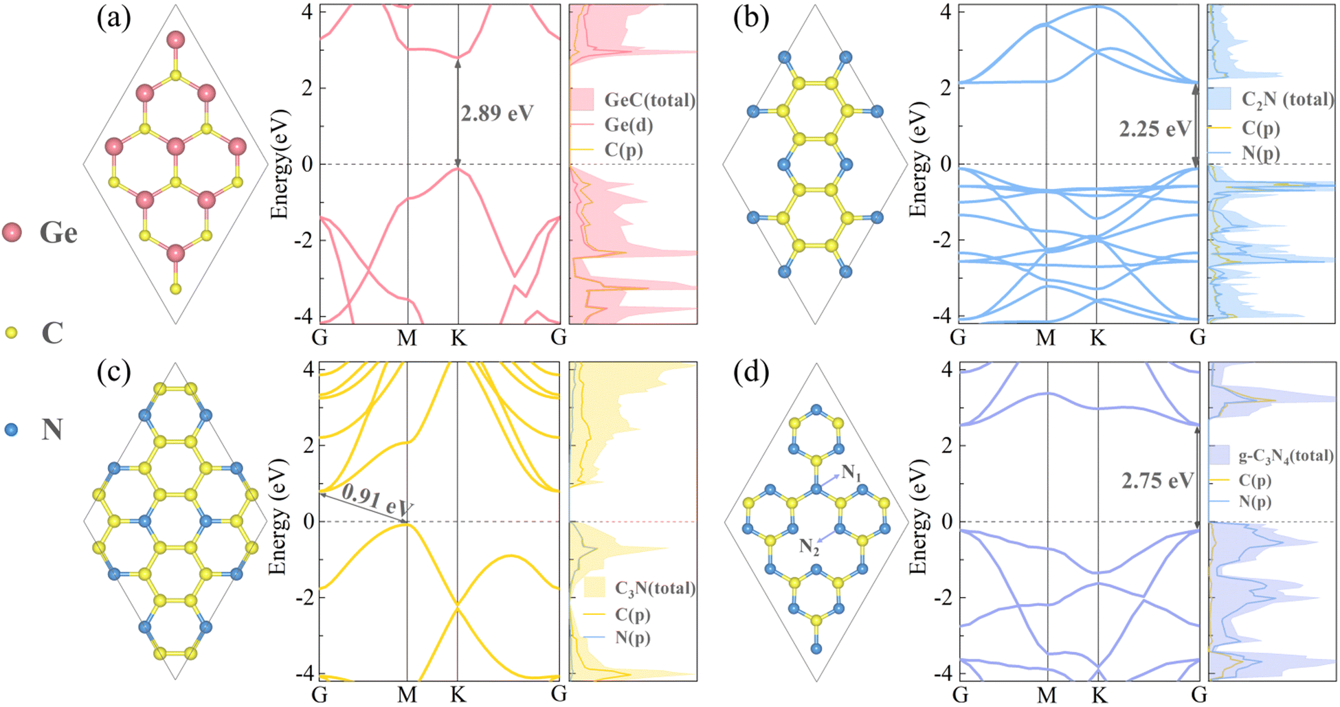
 expanded supercell of the GeC monolayer (8.64 Å), the lattice mismatch ratio is 2.55%. Similarly, when the
  expanded C3N monolayer (8.42 Å) is composite with the
  expanded GeC monolayer (8.64 Å), and the 2 × 2 supercell of the g-C3N4 monolayer (9.56 Å) is composite with the 3 × 3 supercell of the GeC monolayer (9.78 Å), the lattice mismatch ratios are 3.69% and 2.39%. Under these settings, the carbon nitrogen monolayers and GeC monolayer can be perfectly matched to construct suitable heterojunctions, and the subsequent calculations are based on these three lattice configurations.
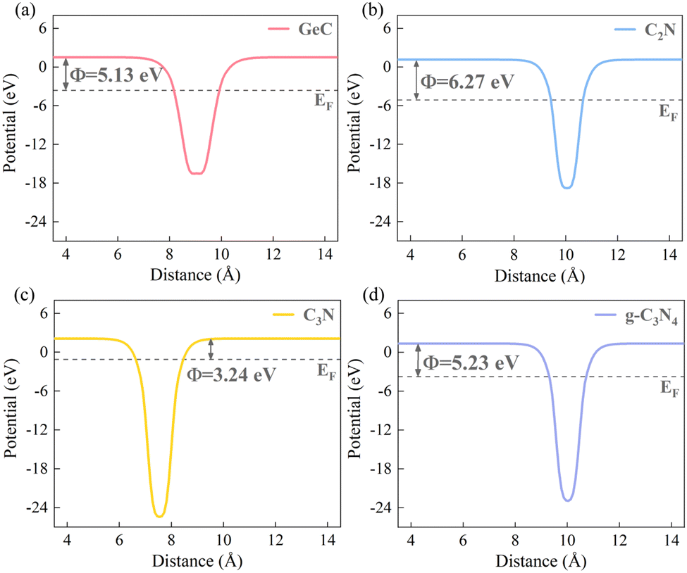
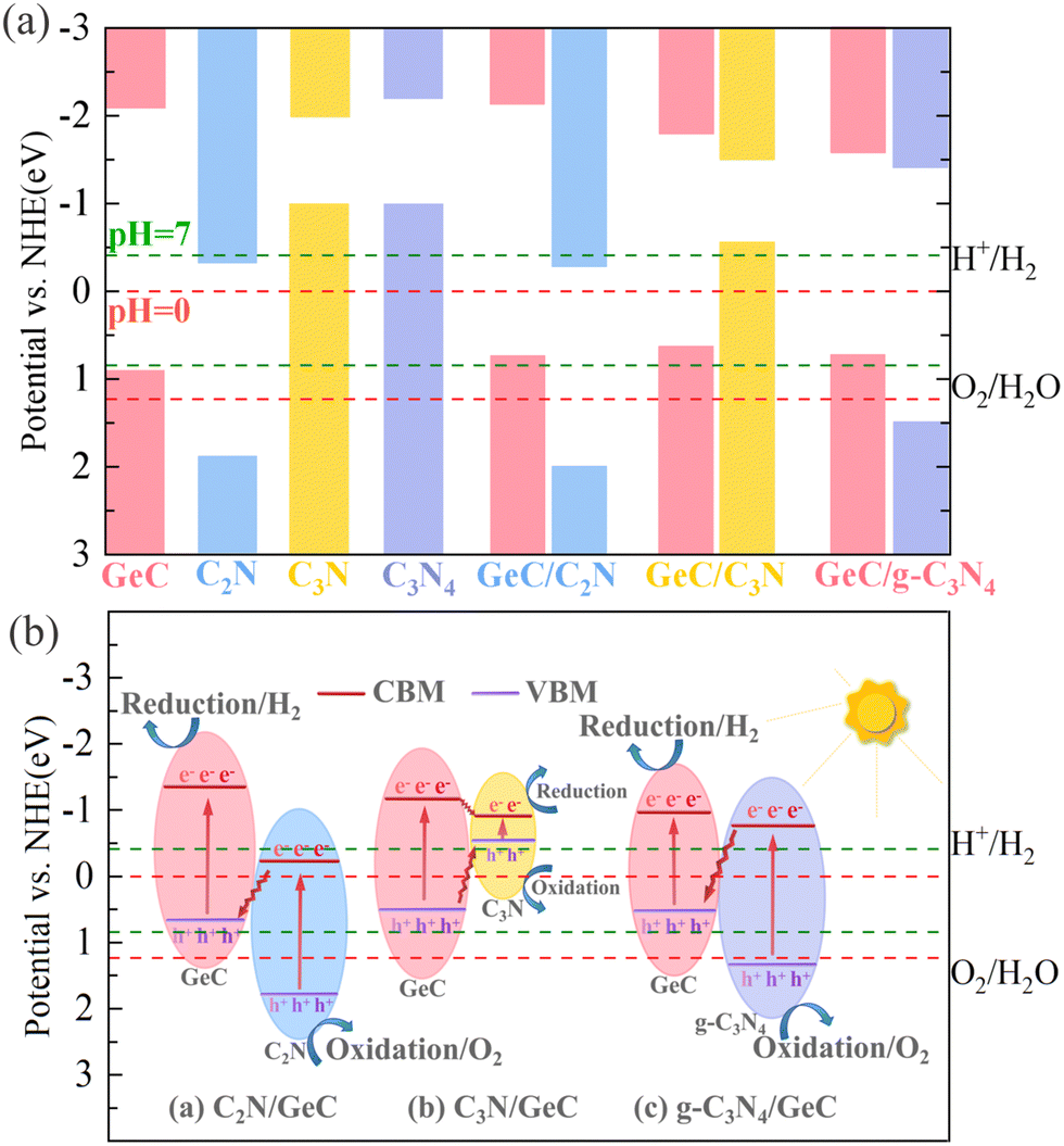
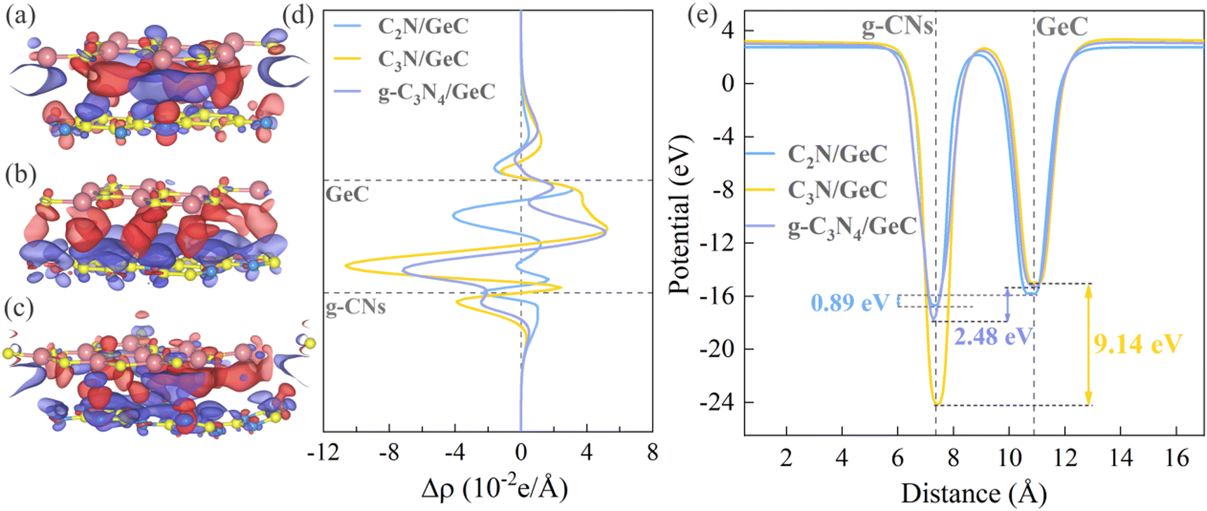
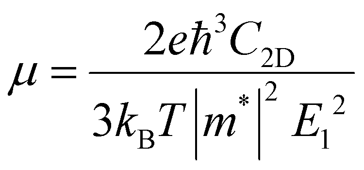

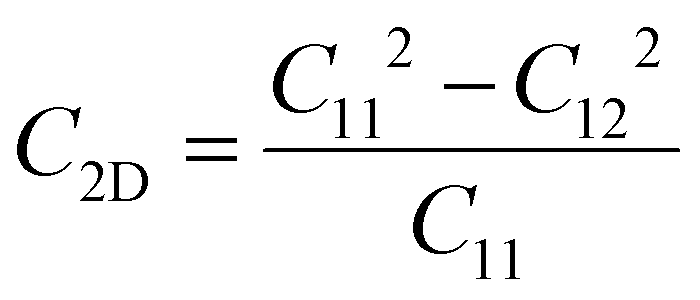
 and
and 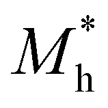 , which can be obtained using formula (5). E(k) and k mean the energy and momentum, respectively. The effective mass of electrons
 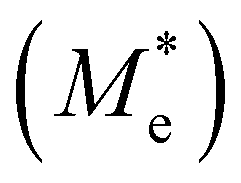 and the effective mass of holes
 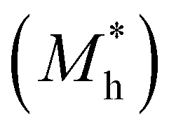 can be obtained by performing a quadratic fit to the band curvatures around the CBM and VBM of the heterojunctions. C2D denotes the elastic modulus of the materials along the transmission direction, which can be calculated by elastic constants, and the relationship between the elastic modulus and the elastic constants is described using formula (6). In addition, E1 is the deformation potential energy constant (DP) of the electrons gathered at the CBM and the holes accumulated at the VBM along the transmission direction, which denotes the linear fitting of band edge changes induced by applying biaxial strains. Fig. 8(a) presents the linearly fitted band edge curves of the CBM (VBM) potentials of the heterojunctions under biaxial strains ranging from −1.5% to +1.5% for the three heterojunctions. The slopes of these curves correspond to the values of the deformation potential constants for electrons (E1e) and holes (E1h). It can be observed that the DP curves are well fitted within the error range. Subsequently, the electron and hole mobility of the three heterojunctions were computed, and the detailed data of carrier mobility are presented in Table 4. It can be observed that both the C2N/GeC and g-C3N4/GeC heterojunctions exhibit small values of
  and large values of
  . Besides, they have similar values of C2D and a relatively small difference of E1e and E1h. Under the circumstances, the carrier mobility was mainly determined by
  and
and  . As a result, both C2N/GeC and g-C3N4/GeC heterojunctions demonstrate high electron mobility and low hole mobility. The μe/μh value of the C2N/GeC heterojunction is 1.79 × 10³/0.57 × 103 cm2 V−1 s−1, and the μe/μh value of the g-C3N4/GeC heterojunction is 2.29 × 10³/0.11 × 103 cm2 V−1 s−1, respectively. Obviously, the carrier mobility of the g-C3N4/GeC heterojunction is higher than that of the C2N/GeC heterojunction. Therefore, the g-C3N4/GeC heterojunction shows a better photocatalytic performance than that of the C2N/GeC heterojunction. This is mainly due to the direct bandgap of the g-C3N4/GeC heterojunction, which eliminates the need for phonon participation when electrons are excited and is more conducive to carrier transition. The excellent carrier mobility of C2N/GeC and g-C3N4/GeC heterojunctions is comparable to many other systems such as PtSe2/GaN,68 InTe/C2N69 and MoSSe/GeC70 heterojunctions. The large carrier mobility means fast migration of photogenerated electrons and holes, enabling carriers to quickly reach the reaction sites and enhancing the photocatalytic activities. Furthermore, there are significant differences in the values of μe and μh in both the Z-scheme heterojunctions, which favor the spatial separation of electron–hole pairs and hinder the recombination of photogenerated carriers. In contrast, although the C3N/GeC heterojunction is not suitable for a photocatalyst, the smaller effective mass gives it excellent electron and hole mobility, The high carrier mobility enables the fast migration of electrons and holes, which is advantageous for its application in optoelectronic fields.
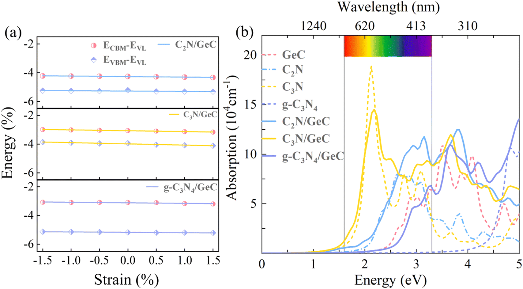
 and
and  ), deformation potential constant (E1e and E1h) and carrier mobility (μe and μh) of the C2N/GeC, C3N/GeC and g-C3N4/GeC heterojunctions