
 Open Access Article
 This Open Access Article is licensed under a
 Creative Commons Attribution 3.0 Unported Licence
Cationic and oxygen defect modulation for tailoring the bandgap and room temperature ferromagnetism of CuO via multiple d-block cations†
Md Shafayatul
Islam
 a,
Koushik Roy
Chowdhury
a,
Sheikh Manjura
Hoque
b and
Ahmed
Sharif
*a
a,
Koushik Roy
Chowdhury
a,
Sheikh Manjura
Hoque
b and
Ahmed
Sharif
*a
aDepartment of Materials and Metallurgical Engineering, Bangladesh University of Engineering and Technology, Dhaka 1000, Bangladesh. E-mail: asharif@mme.buet.ac.bd
bMaterials Science Division, Atomic Energy Centre, Dhaka, Bangladesh
First published on 6th February 2024
Abstract
The potential of oxide-based dilute magnetic semiconductors (DMSs) for use in spintronics and magneto-optic devices has garnered a lot of attention over the years. However, the optical and magnetic behavior of these DMSs is challenging to navigate due to the complicated interactions of intrinsic defects. In these contexts, the current research takes a comprehensive look at the pristine and simultaneously multiple d-block cation (Cr, Fe, Ni, Co, and Zn)-doped CuO nanocrystals (NCs) to explain the defect interactions inside the lattice. Structural analysis revealed a highly crystalline monoclinic crystal structure in the C2/c space group. The phase stability of CuO NCs was found to decrease with increasing dosages of dopants, ultimately forming a secondary phase of Cu metal. Diffuse reflectance spectroscopy (DRS) spectra showed narrowing of the optical band gap, attributing it to the presence of impurity states between the conduction band minimum (CBM) and valence band maximum (VBM) as a result of doping. These impurity states can inhibit carrier recombination. Both pristine and doped CuO NCs showed ferromagnetism at ambient temperature with a paramagnetic tail at higher fields. This paramagnetic tail, explained based on the thermomagnetization curves, corresponds to the easy flip of magnetic cations below room temperature. All the ferromagnetic features of CuO NCs may be traced back to the exchange interaction between the spins of magnetic ions, mediated by carrier-trapped vacancy centers. Interestingly, doped oxides showed improved ferromagnetism when used at moderate concentrations, which is related to the creation of a larger number of bound magnetic polarons (BMPs). However, higher dosages of dopants lower the concentration of BMPs by delocalizing the carriers from the defect centers.
Introduction
The demand for metal oxide (MO) nanostructures is growing and has attracted noticeable research interest due to their alluring fundamental properties like structural, optical, and magnetic properties, which enable their multidisciplinary implementation in various sensors, supercapacitors, solar cells, catalysis, photocatalysis, spintronic devices, and so on.1–7 Particularly, p-type cupric oxide (CuO) semiconducting nanocrystals (NCs) are receiving more attention as multifunctional materials because of their fundamental properties, i.e., narrow bandgap (1.2–1.8 eV) and room-temperature ferromagnetism (RTFM).8 CuO also possesses environmental compatibility, non-toxicity, eco-friendliness, high theoretical capacity, and increasing susceptibility at low temperatures, which make it a potential contender for the energy domain, antibacterial applications, light-emitting diodes (LEDs), and degradation of organic pollutants.9,10In addition, CuO is a potential candidate for oxide-based dilute magnetic semiconductors (DMSs), which are promising future materials for spintronic applications due to their versatility in spin transport, spin detection, and spin filtering.11 For these applications, possession of room-temperature ferromagnetism (RTFM) is essential for DMSs, which is arguably intriguing and the most mysterious problem in magnetism. Hence, the discovery of RTFM in CuO has been a core area of research interest, which is probably affected by defect equilibrium in the crystal lattice. A feasible mechanism for inducing RTFM could be the modulation of defects by incorporating dopant elements such as d-block cations. These dopants can tailor ferromagnetism as well as the position of Fermi energy levels through the interaction of the 3d orbital electrons, thus tuning the magnetic, optical, and electric properties of the host CuO.
Several researchers have reported that doping CuO with d-block elements causes a dramatic shift in its physicochemical properties and forms new types of materials with enhanced physical and chemical characteristics without any major modification of the host CuO structure that has interesting spin-dependent electrical, optical, and magnetic properties. These new properties are attributed to modifications of the bandgap, alteration of the electronic structure, sp–d exchange interactions that involve the d-sub-levels of d-block ions, and holes in the valence band of the host semiconductor. For example, band gap values were modified and found to increase as the doping concentration of Cr increased in CuO.12 In addition, Cr can induce RTFM in CuO.13 Further, it was observed that Co-doped CuO nanoparticles show superparamagnetism at room temperature.14 One important finding is that Fe dopants in CuO prefer to align anti-parallel to one another, while Fe dopants in larger numbers tend to align parallel to one another.15 The absorption peak of Ni-doped CuO nanoparticles moves towards a higher wavelength, i.e., a redshift, and the magnetization goes up with Ni concentration up to 5 mol% doping, and further increases in Ni content decrease the magnetization.16 With increasing the doping concentration of Zn, the band gap edge shifted towards the longer wavelength region.17 However, the origin of the improved ferromagnetic behavior of CuO doped with non-magnetic cations (such as Zn2+) has been the subject of relatively few investigations. These reports of RTFM in undoped, magnetically doped, and non-magnetically doped CuO all point towards the significance of defects in generating ferromagnetic ordering as well as customizing bandgaps.
In general, a significant amount of oxygen vacancies, along with other point defects, are common on the surface of nanoscale semiconductors like CuO because of the size effects.18 The point defects strongly affect the energy states, which can modify the optical and magnetic characteristics. Therefore, point defects like lattice oxygen as well as cation vacancies, interstitials, and free charge carriers act as controlling factors for tailoring the bandgap and transport properties of dilute magnetic semiconductors (DMSs) like CuO. The next natural step going forward would be to study how the incorporation of these defects in different concentrations and configurations affects the optical and magnetic properties of this structure.
Moreover, it is observed that the physical properties of CuO NCs are also affected by the morphology, structure, and size of the nanocrystals, which in turn depend on the specific synthesis method.19,20 Several research groups synthesized CuO NCs by chemical, physical, and biological methods such as hydrothermal, co-precipitation as well as green-mediated combustion, microwave irradiation, and sol–gel.9,21 These methods are capable of producing nanoscale particles with various shapes, sizes, morphologies, and dimensions, such as zero-dimensional (0D) nanoparticles, one-dimensional (1D) nanorods, two-dimensional (2D) complex interconnecting nanosheets, and three-dimensional (3D) nanoflowers, to explore the intriguing application of CuO NCs by tuning different parameters like pH, time, temperature, and capping agents. Among these, sol–gel is of great interest as it is economical, eco-friendly, and has an impact on the size of the NCs and the formation of defects like point defects, dislocations, vacancies, and others.
After reviewing the available literature, it has become clear that little work has been done so far to determine the collective effect of simultaneously doping multiple d-block elements on defect modulation of metal oxides such as CuO. Therefore, pristine and multiple d-block element-doped CuO NCs were successfully synthesized via a modified sol–gel method with varying concentrations in the present work. To determine the experimental origin of ferromagnetism in DMSs and to pave the path for the growth of spin electronic devices, the synthesized samples (pristine and doped CuO NCs) will be connected to physical and structural changes caused by doping. A clear picture of mysterious defect interactions inside the inorganic CuO structure via localization and delocalization of carriers at various defect centers due to defect modulation is depicted. This fundamental study provides useful insights into the broad implications across multiple domains like water splitting, photocatalysis, and dilute magnetic semiconductors. Furthermore, it paves a way to regulate the same monoclinic CuO structure for a variety of applications by tailoring bandgap and room-temperature ferromagnetism through multiple d-block cation doping and also gives a base to understand the bound magnetic polaron interactions in the presence of multiple magnetic and nonmagnetic impurities. Consequently, this study aimed to evaluate the physicochemical properties of pristine CuO and the effectiveness of simultaneously incorporating multiple d-block elements (Cr, Fe, Co, Ni, and Zn) to assess its modified structural, morphological, optical, and magnetic properties extensively via defect chemistry for assigning suitable applications in terms of structural distortion, particle size, bandgap, band-position, and magnetism.
Materials and methods
Materials
All of the chemical reagents used in the synthesis process were of analytical grade. Copper(II) nitrate trihydrate [Cu(NO3)2·3H2O] was used as a precursor; ethylene glycol [C2H6O2] was used as a chain transfer agent; citric acid [C6H8O7] was used as a network former; and deionized water was used as a solvent. Chromium(III) nitrate nonahydrate [Cr(NO3)3·9H2O], iron(III) nitrate nonahydrate [Fe(NO3)3·9H2O], cobalt(II) nitrate hexahydrate [Co(NO3)2·6H2O], nickel(II) nitrate hexahydrate [Ni(NO3)2·6H2O], and zinc(II) nitrate hexahydrate [Zn(NO3)2·6H2O] were used as the dopant source with varying amounts for different doping concentrations.Synthesis of nanocrystals
Pristine CuO and doped Cu1–5x(CrFeCoNiZn)xO (where x = 0.01, 0.02, and 0.03) NCs were synthesized following the modified sol–gel method. A 0.3 M clear precursor solution was prepared by dissolving 5 g of Cu(NO3)2·3H2O into deionized water and raising the temperature to 80 °C along with continuous vigorous stirring at 400 rpm. The precursor solution was then treated with citric acid. After the complete dissolution of citric acid, ethylene glycol was added drop by drop into the solution. The precursors, citric acid and ethylene glycol, had a 1![[thin space (1/6-em)]](https://www.rsc.org/images/entities/char_2009.gif) :2:6 molar ratio. A thick gel was created after prolonged heating and stirring. The gel was dried at 120 °C for 20 hours in an electric oven. A fine green powder was formed by crushing the dried gel. To achieve crystallization, the green powder was annealed for 1 hour at 500 °C at a heating rate of 5 °C minute−1. Finally, a black powder of CuO NCs was obtained. For doping of d-block cations, proper stoichiometric proportions of chromium(III) nitrate nonahydrate [Cr(NO3)3·6H2O], iron(III) nitrate nonahydrate [Fe(NO3)3·9H2O], cobalt(II) nitrate hexahydrate [Co(NO3)2·6H2O], nickel(II) nitrate hexahydrate [Ni(NO3)2·6H2O], and zinc(II) nitrate hexahydrate [Zn(NO3)2·6H2O] were added into the solution simultaneously to obtain doped Cu1–5x(CrFeCoNiZn)xO NCs where x = 0.01, 0.02, and 0.03. For simplification, doped Cu1–5x(CrFeCoNiZn)xO NCs are denoted as CuO-a, CuO-b, and CuO-c for x = 0.01, 0.02, and 0.03, respectively. According to their respective precursors, Co, Ni, and Zn atoms are doped in the +2 valence state, whereas Fe and Cr atoms are doped in the +3 valence state. The schematic diagram corresponding to the complete synthesis route of the NCs is presented in Fig. 1.
:2:6 molar ratio. A thick gel was created after prolonged heating and stirring. The gel was dried at 120 °C for 20 hours in an electric oven. A fine green powder was formed by crushing the dried gel. To achieve crystallization, the green powder was annealed for 1 hour at 500 °C at a heating rate of 5 °C minute−1. Finally, a black powder of CuO NCs was obtained. For doping of d-block cations, proper stoichiometric proportions of chromium(III) nitrate nonahydrate [Cr(NO3)3·6H2O], iron(III) nitrate nonahydrate [Fe(NO3)3·9H2O], cobalt(II) nitrate hexahydrate [Co(NO3)2·6H2O], nickel(II) nitrate hexahydrate [Ni(NO3)2·6H2O], and zinc(II) nitrate hexahydrate [Zn(NO3)2·6H2O] were added into the solution simultaneously to obtain doped Cu1–5x(CrFeCoNiZn)xO NCs where x = 0.01, 0.02, and 0.03. For simplification, doped Cu1–5x(CrFeCoNiZn)xO NCs are denoted as CuO-a, CuO-b, and CuO-c for x = 0.01, 0.02, and 0.03, respectively. According to their respective precursors, Co, Ni, and Zn atoms are doped in the +2 valence state, whereas Fe and Cr atoms are doped in the +3 valence state. The schematic diagram corresponding to the complete synthesis route of the NCs is presented in Fig. 1.
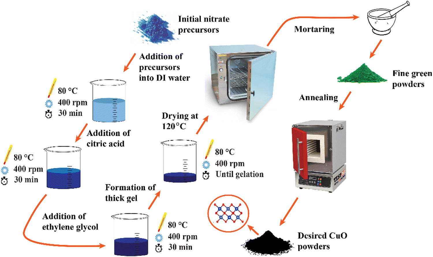 | ||
| Fig. 1 Schematic diagram of the CuO NC synthesis route. | ||
Characterization
The structural studies of the synthesized NCs were characterized using an X-ray diffractometer (Rigaku) at RT using a Cu X-ray source of wavelength Kα1 = 1.5406 Å and a scanning rate of 5° minute−1 for Bragg angles (2θ) ranging from 10° to 80°. Further, the Rietveld refinement was performed using HighScore Plus, and the percent crystallinity was calculated with OriginPro software. A Thermo Fisher Scientific Escalab Xi+ was used to take X-ray photoelectron spectroscopy (XPS) readings with Al Kα radiation to confirm the presence of various oxidation states on the surface of NCs. The morphological and structural analyses of NCs were estimated using the micrographs collected on a field emission scanning electron microscope (FE-SEM: JEOL, JSM, 7600F). The micrographs of the synthesized samples were also observed by high-resolution transmission electron microscopy (HR-TEM: Talos F200X, Thermo Fisher Scientific, USA). The TEM sample was prepared by sonicating a tiny amount of the materials in 2 mL of ethanol for 20 minutes. The sonicated sample was placed on a 3 mm Cu grid that was carbon-coated. After letting the material dry, it was examined under a microscope. By utilizing Gatan and ImageJ software, the images from SEM and TEM were analyzed. The elemental presence of the materials was measured using an EDX attached to a TEM. UV-Vis spectroscopy (model: LAMBDA 1050, PerkinElmer, USA) was used to obtain UV-Vis diffuse reflectance spectra of both pristine and doped CuO NCs. To determine the indirect band gaps of pristine and doped CuO NCs, the Kubelka–Munk function was applied to the corresponding diffuse reflectance spectra. Using a Quantum Design Physical Property Measurement System (Quantum Design PPMS EverCool-II), its room-temperature magnetic properties were studied from −20 kOe to 20 kOe. Furthermore, a Quantum Design PPMS was used to measure magnetization from 5 K to 400 K.Results and discussion
Structural information (XRD analysis)
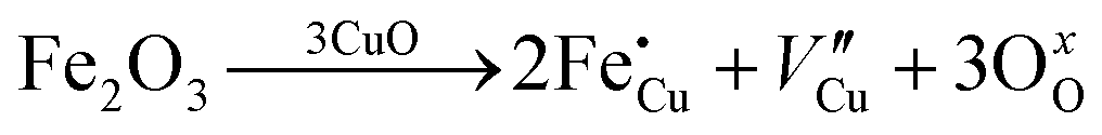
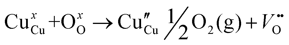
The room-temperature X-ray powder diffraction (XRD) spectra of pristine CuO and doped CuO NCs are depicted in Fig. 2a. These spectra were studied by using the Rietveld refinement method to confirm the crystallographic structure, phase, and crystallinity of the NCs. Fig. 3 depicts the refined curves of CuO, CuO-a, CuO-b, and CuO-c, respectively. The diffraction peaks located at 32.48°, 35.52°, 38.67°, 46.24°, 48.74°, 51.29°, 53.44°, 58.2°, 61.52°, 65.76°, 66.24°, 68.06°, 72.33°, and 75.46° by pristine CuO can be ascribed to the (110), (11−1), (111), (11−2), (20−2), (112), (020), (202), (11−3), (022), (31−1), (220), (311) and (22−2) planes, respectively, which confirmed the polycrystalline monoclinic structure of tenorite CuO NCs with a C2/c space group and matched strongly with JCPDS card no. 80-1268.22 Notably, no impurity phases were identified in the XRD spectra, which confirms the purity of the synthesized pristine CuO NCs. Furthermore, it can be noted that doped CuO-a NCs also did not exhibit any additional unexpected peaks, which indicates that Cr, Fe, Co, Ni, and Zn ions have been substituted into Cu sites without destroying the monoclinic structure due to the almost similar effective ionic radii of Cu2+ and dopants,23 which greatly increases the likelihood of the substitutional replacement in the CuO crystal lattice. However, in the case of CuO-b and CuO-c NCs, an extra diffraction peak (marked by an asterisk (*) in Fig. 2a) emerges inside the structure. This diffraction peak observed at 43.59° for CuO-b and 43.39° for CuO-c (as shown in the enlarged image of Fig. 2b for 2θ = 42°–45°) corresponds to the crystal plane (111) of a single cubic phase metallic Cu (space group: Fm![[3 with combining macron]](https://www.rsc.org/images/entities/char_0033_0304.gif) m, JCPDS card no. 85-1326),24 which can contribute to the optical and magnetic properties of the NCs.25,26 Doped CuO NCs may exhibit the impurity phase (metallic Cu) as a result of the reduction of the CuO phase by the carrier electrons that might be generated due to the formation of oxygen vacancies, which can give up free electrons. During annealing, O2− leaves its sites, forming an oxygen vacancy, and by accepting the electrons, the Cu2+ ion can undergo a phase transformation into the metallic Cu phase. Kröger–Vink notations provide the following expression of the probable defect reactions:
m, JCPDS card no. 85-1326),24 which can contribute to the optical and magnetic properties of the NCs.25,26 Doped CuO NCs may exhibit the impurity phase (metallic Cu) as a result of the reduction of the CuO phase by the carrier electrons that might be generated due to the formation of oxygen vacancies, which can give up free electrons. During annealing, O2− leaves its sites, forming an oxygen vacancy, and by accepting the electrons, the Cu2+ ion can undergo a phase transformation into the metallic Cu phase. Kröger–Vink notations provide the following expression of the probable defect reactions: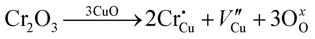 | (1) |
 | (2) |
 | (3) |
| Cu2+ + 2e′′ = Cu | (4) |
 | (5) |
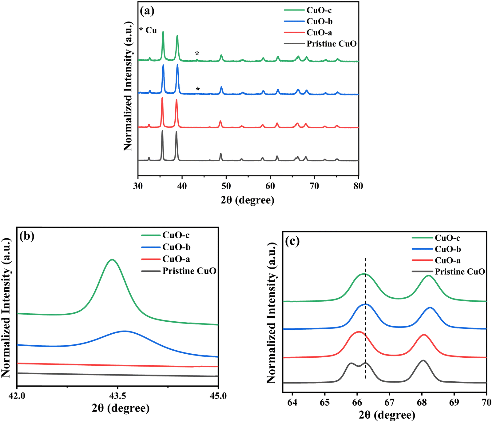 | ||
| Fig. 2 (a) Room temperature XRD patterns of pristine CuO, CuO-a, CuO-b, and CuO-c. (b) Refined spectra show the appearance of the secondary Cu phase. (c) Refined spectra show the merging of a split peak into a single peak. | ||
 | ||
| Fig. 3 Rietveld refinement of the nanocrystals. | ||
The necessary explanation of the symbols is included in the ESI.† The merging of the split peak of pristine CuO into a single peak (as shown in Fig. 2b) in doped CuO NCs towards larger angles indicates a slight distortion in the symmetry of the monoclinic system due to the creation of a charge imbalance by Fe3+ and Cr3+ ion doping as a replacement for Cu2+ in the copper oxide lattice.27 Hence, from these defect reaction analyses (eqn (1)–(5)), defects generated in the system can be attributed to the charge imbalance that occurs from Cr3+ and Fe3+ incorporation, which leads to cation vacancies along with oxygen vacancies.
All the diffraction peaks are very intense and sharp, which indicates the strong, well-ordered polycrystalline nature of the synthesized materials.28 However, the intensities of the (11−1) and (111) planes are much higher than those of the rest of the peaks, indicating a prominent orientation of the formed crystallites along either of these directions, which will later be confirmed by TEM observation. For higher doping concentrations of CuO-b and CuO-c, a sharp fall in intensity is noticed, which may happen due to the disorder caused by the disparity in ionic size between the dopant and parent ions. The decrease in peak intensity is attributable to a reduction in the crystallinity of the CuO NCs as doping induces a lattice strain phenomenon in the CuO matrix.29 The peak broadening of the doped NCs compared to pristine CuO is also strain-induced and can be attributed to various reasons, e.g., the formation of smaller particle sizes as well as defects in the lattice structure.29 The calculated values of a, b, and c lattice parameters obtained from the Rietveld refinement, along with the constituent phases, space group, unit cell volume, bond length, bond angle, and reliability (R) factors of the Rietveld refinement, are listed in Table S1 (ESI†). The following equation for monoclinic lattices was used in Rietveld refinement to find the lattice parameters:30
 | (6) |
β. As can be seen from Table S1 (ESI†), the variation of the unit cell volumes does not follow a systematic trend with increasing concentration of dopants due to the complicated monoclinic structure of CuO NCs and ionic radius variation in the dopant ions. The volumes are in the range of 81.121–81.256 Å3.
As discussed earlier, the amount of dopant present in CuO NCs is inversely proportional to the degree of crystallization. In addition, we have used the Rietveld refined XRD spectra to quantitatively measure the crystallinity of the samples using the following equation:31
 | (7) |
θ, we have calculated the interlayer spacing “d” of the (11−1) characteristic plane before and after doping with d-block cations. The crystallite sizes of the NCs were determined using Scherrer's formula. Scherrer's formula32 can be written as follows: | (8) |
 | (9) |
| Samples | d (Å) (11−1) plane | Crystallite size (Scherrer's formula), D (nm) | Microstrain, ε ×10−3 | Dislocation density, δ × 10−3 (nm−2) | Crystallinity (%) |
|---|---|---|---|---|---|
| Pristine CuO | 2.525 | 32.94 | 1.8 | 0.92 | 92.18 |
| CuO-a | 2.527 | 28.01 | 2.1 | 1.27 | 90.92 |
| CuO-b | 2.512 | 24.3 | 2.4 | 1.69 | 87.03 |
| CuO-c | 2.514 | 25.1 | 2.3 | 1.587 | 89.31 |
Further, the microstrain was calculated using the following equation:33
 | (10) |
All these parameters (percentage crystallinity, d spacing, crystallite size, dislocation density, and lattice strain) were calculated corresponding to the characteristic (11−1) peak and are tabulated in Table 1.
Notably, from Table 1, the “d” values corresponding to the (11−1) plane of pristine CuO, CuO-a, CuO-b, and CuO-c are found to be 2.525, 2.527, 2.512, and 2.514 nm, respectively. This variation is due to the slight shift of the (11−1) peak compared to pristine CuO owing to the lattice distortion of the synthesized doped NCs. Higher d spacing between (11−1) planes in pristine CuO and CuO-a along the [11−1] direction ensures fast ion transport between (11−1) planes.34
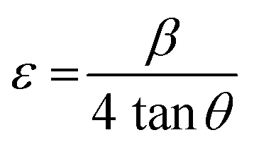
Moreover, as can be observed from Table 1, the crystallite size first falls when the doping concentration is raised. Dopant ions at the grain boundaries may be to blame for this, since the dopant ions increase the energy barrier for the diffusion of Cu2+ ions and so restrict the expansion of the crystal, creating smaller crystallite size.35 Thus, the role of impurities, i.e., dopant atoms, is to impede grain growth by segregating to the grain boundaries, which might have happened for the CuO-a and CuO-b NCs. However, a further increase in doping concentration (CuO-c) enhances the interaction between the dopant ions, which in turn reduces the effectiveness with which they may settle at the grain boundaries. This leads to enhanced growth of CuO-c crystallites as well as a reduction of microstrain (ε), as observed from the XRD pattern analysis. The reduction in micro-strain is obtained from 2.4 × 10⁻³ for CuO-b to 2.3 × 10⁻³ for CuO-c, which signifies a decrease in lattice imperfections, an increase in lattice parameter “a” (as shown in Table S1, ESI†), and the construction of a more dislocation-free lattice, which is confirmed by the reduced value of dislocation density for CuO-c NCs. Therefore, with a larger D, the internal strain in the crystal is at a minimum, and there are fewer dislocations per unit area (Fig. 4).
 | ||
| Fig. 4 Variation of crystallite size, microstrain and dislocation density as a function of doping concentration. | ||
Using Rietveld refinement data, VESTA was used to calculate the bond lengths and bond angles of the NCs (as depicted in Fig. S1 (ESI†) for pristine CuO). From Table S1 (ESI†), it is seen that changes in bond length show a similar tendency to the lattice parameter “a”. The Cu–O–Cu bond angle shows a decreasing tendency up to the CuO-b doping level, then increases, which is also in good accordance with the evolution of crystal size. This finding suggests that the variation of the lattice parameter “a” and the size of the particles is controlled by the bond angles and bond lengths.
The formation of Cu vacancies to ensure charge balance will decrease the number of Cu–O bonds and lead to a reduction in the Cu–O–Cu bond angle compared to pristine CuO, as evidenced from Table S1 (ESI†). The reduced Cu–O–Cu bond angle and increased Cu–O bond length indicate distortion of the lattice. However, the Cu–O bond length is shown to suddenly drop with greater doping concentrations of CuO-c due to the increased likelihood of dopants residing at the interstitial site. These interstitial dopant ions may influence the lattice via their interactions with other copper or oxygen ions, resulting in a fluctuation in CuO bond length. Hence, dopant concentration is crucial in regulating the intrinsic lattice orientation and defect density of the host system.
Surface chemical analysis (by XPS)
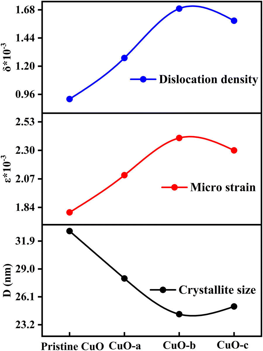
X-ray photoelectron spectroscopy (XPS) was used to analyze the chemical composition, valence, and electronic states of the host and dopant elements in the samples based on their corresponding binding energies. The XPS survey spectra are displayed in Fig. 5. The Cu 2p peak in the 930–965 eV range is clearly apparent for both pristine CuO and CuO-c NCs, together with the prominent Auger peaks. Moreover, doped CuO-c contains peaks of Zn 2p, Ni 2p, Co 2p, Fe 2p, and Cr 2p spectra, demonstrating that their respective atoms are present. The narrow scan spectra of these atoms are displayed in Fig. 6a–i. The Shirley background subtraction of the spectrum is used for all atoms. | ||
| Fig. 5 Survey spectra of (a) pristine CuO NCs and (b) CuO-c NCs. | ||
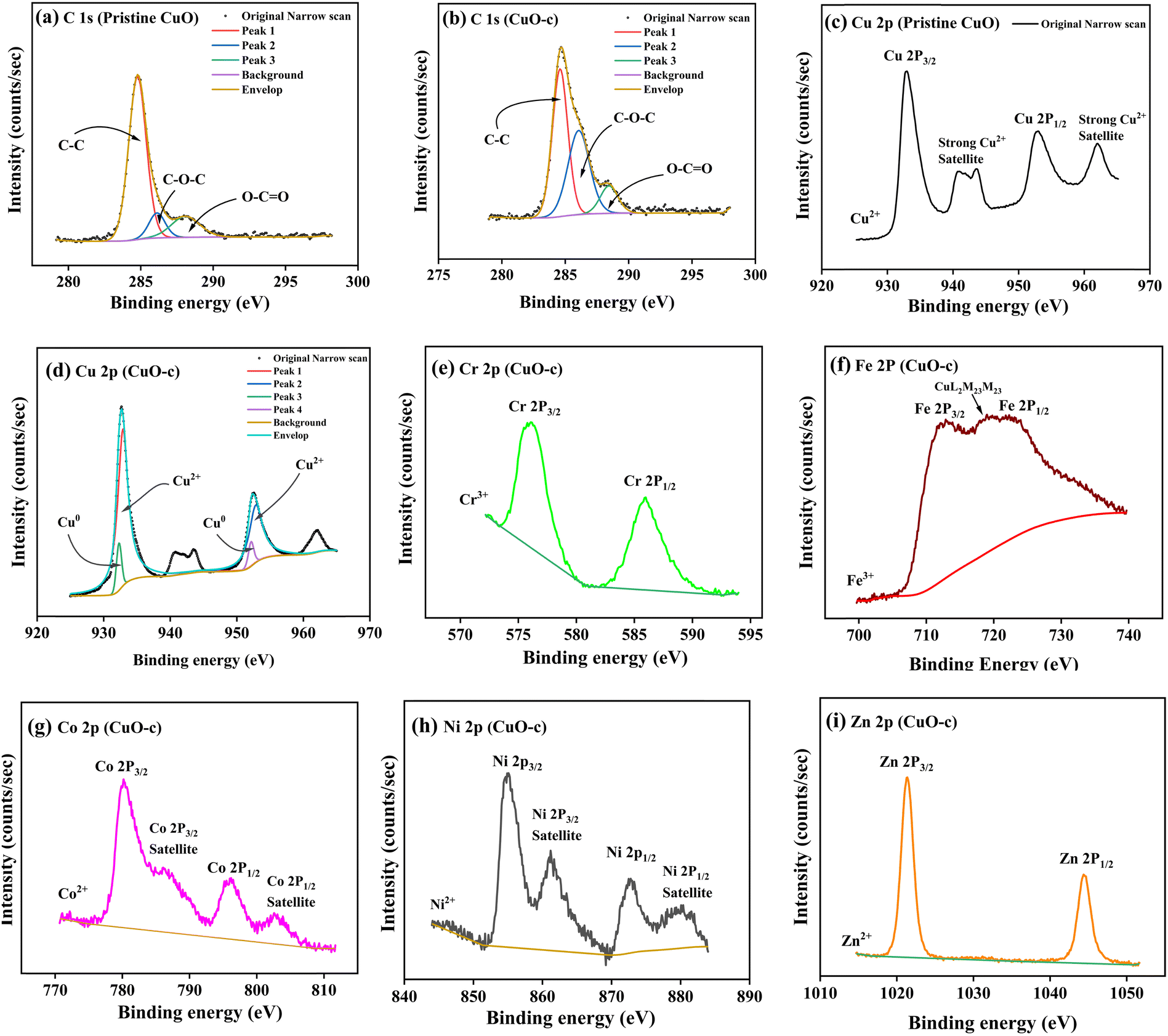 | ||
| Fig. 6 High-resolution spectra of (a) C 1s from pristine CuO, (b) C 1s from CuO-c, (c) Cu 2p from pristine CuO, (d) Cu 2p from CuO-c, (e) Cr 2p from CuO-c, (f) Fe 2p from CuO-c, (g) Co 2p from CuO-c, (h) Ni 2p from CuO-c, and (i) Zn 2p from CuO-c. | ||
Fig. 5 shows no unintentional impurity, except carbon, in both samples. Surface contamination accounts for the occurrence of the C 1s peak in the survey spectra. The high-energy resolution spectrum of the C 1s envelope for pristine CuO as well as CuO-c was fitted with three peaks, as shown in Fig. 6a and b. For pristine CuO, the C–C bond peak was located at 284.8 eV, the C–O–C peak at 286.1 eV, and the O–C![[double bond, length as m-dash]](https://www.rsc.org/images/entities/char_e001.gif) O peak at 288.1 eV.36 The binding energy of the C 1s peak at 284.8 eV was utilized as a charge reference in the XPS experiments. For the doped CuO-c sample, regarding these peaks, a small shift in binding energy is observed. Peaks at 284.6 eV, 286.1 eV, and 288.5 eV for CuO-c correspond to C–C, C–O–C, and O–CO bonds, respectively. The shift of the binding energy peaks of the doped sample compared to the pristine CuO can be attributed to the difference in the electronegativity values of Cu and dopant elements.
O peak at 288.1 eV.36 The binding energy of the C 1s peak at 284.8 eV was utilized as a charge reference in the XPS experiments. For the doped CuO-c sample, regarding these peaks, a small shift in binding energy is observed. Peaks at 284.6 eV, 286.1 eV, and 288.5 eV for CuO-c correspond to C–C, C–O–C, and O–CO bonds, respectively. The shift of the binding energy peaks of the doped sample compared to the pristine CuO can be attributed to the difference in the electronegativity values of Cu and dopant elements.
High-resolution scans of the Cu 2p spectra are shown in Fig. 6c and d. As depicted in Fig. 6c, the pristine CuO NCs consisted of a doublet of Cu 2p3/2 at 933.0 eV and Cu 2p1/2 at 953.0 eV with an energy difference of 20 eV, which is consistent with the standard spectrum of CuO.37 That is to say, the Cu ions undergo oxidation during the reaction. The energy difference between 2p3/2 and 2p1/2 was due to the spin–orbit coupling. In this spectrum, the peaks centered at 941 and 943.7 eV are assigned to satellite peaks for 2p3/2, with 8 and 10.7 eV higher binding energies than those of the main peak. Since Cu2O and Cu do not include shake-up satellites, their existence in Cu 2p spectra may be attributed to CuO NCs.38 This, together with the broad nature of the Cu 2p3/2 peak, confirms the prevailing presence of the Cu2+ state, indicating that +2 is the only valence for Cu ions in undoped NCs. The XPS spectrum of doped Cu 2p is deconvoluted using 20% Gaussian and 80% Lorentzian functions (as depicted in Fig. 8d) into two separated fitted pairs of peaks at 932.3 and 952.2 eV, revealing the co-existence of Cu0 states with Cu2+ at the surface of the CuO-c NCs. Thus, in CuO-c, the Cu 2p spectrum consists of cubic Cu and monoclinic Cu2+ ions, respectively, which was also observed from XRD analysis. However, the peaks of Cu 2p3/2 and Cu 2p1/2 in doped CuO-c NCs are slightly shifted to lower (redshift) binding energies as compared with those of pristine CuO NCs at 932.9 eV and 952.9 eV, respectively. The slight shift of binding energy indicates that the modification in the bond length of CuO, as confirmed by XRD, is due to the incorporation of dopant ions in the CuO lattice.
The high-resolution scan of the XPS spectrum of Cr 2p is shown in Fig. 6e, which indicates the peak of Cr 2p3/2 detected at 576.1 eV for the CuO-c NCs. The peak is near the peak of the Cr3+ state but is different from 574.3 eV for Cr metal, 579 eV for Cr4+, and 576.0 eV for the Cr2+ state.39 This indicates that Cr3+ ions are incorporated into the CuO lattice as dopants. The Cr 2p1/2 peak appears at 585.9 eV. The satellite feature of the Cr 2p3/2 peak overlaps the Cr 2P1/2 component in Cr2O3.
Fig. 6f shows that the Fe 2p spectrum is split into Fe 2p3/2 at 711.8 eV and Fe 2p1/2 at 724 eV due to spin–orbit interaction. Due to interference from a prominent Auger peak of Cu L3M23M23 from copper, it is challenging to further utilize the Fe 2p doublet for quantitative purposes.30 The absence of a peak at 706–707 eV rules out the presence of metallic Fe in doped samples.40 The peaks are in good agreement with those for Fe2O3 (B.E. ∼710–711 eV). These results show that the valence of Fe ions is mostly +3. In other words, Fe3+, rather than Fe2+, takes the position of Cu2+ in the crystal lattice. It is clear why the concentration of cation vacancies and the concentration of Fe ions or Cr ions follow a similar trend. Hence, the more the Fe3+ and Cr3+ ions are replacing Cu2+, the greater the vacancy percentage is needed to accommodate the charge conservation rule.
The signature of cobalt in the NCs was evident from the high-resolution XPS spectrum in Fig. 6g, corresponding to the core levels of two spin–orbit doublets, Co 2p3/2 at 780.3 eV and Co 2p1/2 at 796.18 eV.41 The spin–orbit splitting of 15.9 eV is in good agreement with the literature report of Co, present in the +2 oxidation state. In addition to this, two satellite peaks also occur at higher binding energies (786.1 eV and 802.6 eV).41
In Fig. 6h, the Ni 2p spectrum exhibits two peaks at 855 and 872.5 eV, which are in good agreement with the binding energies of Ni 2p3/2 and Ni 2p1/2, respectively,42 indicating the presence of the Ni2+ state. Besides, the satellite peaks of Ni 2p located at 861.2 and 880.1 eV also prove the existence of the Ni2+ (Ni–O bonds) state.43
The peaks that are visible in Fig. 6i were assigned to Zn 2p3/2 and Zn 2p1/2, which were positioned at 1021.4 eV and 1044.4 eV, respectively. The Zn 2p core electron level is unreliable for distinguishing Zn from ZnO according to XPS literature. For this purpose, the Zn Auger peak (L3M45M45) was recorded as depicted in Fig. S2 (ESI†) and α, the Zn Auger parameter, was calculated (α = BE (Zn 2p3/2) + KE (Zn Auger), where KE is the kinetic energy of the Auger electron). Here, α = 1021.4 + 989.3 eV = 2010.7 eV and fits in with ZnO, of which α values are reported to be in the 2009.5–2011 eV range. Thus, the Auger parameter obtained in this work is much lower than that of metallic zinc (2013.4–2014.4 eV),30 which agrees with reported values for ZnO in the 2009.5–2011 eV range. Therefore, the resulting Auger parameter is much less than the value for metallic zinc (2013.4–2014.4 eV), implying that Zn oxidized (as Zn2+) in the CuO NCs.
Fig. 7a depicts the O 1s spectrum of the pristine CuO sample. The O 1s peak revealed an asymmetrical trend with two broad humps, pointing to the existence of oxygen species with multiple components found in the near-surface area. The high-resolution XPS spectrum of O 1s was fitted using three Gaussian components corresponding to three peaks at 529.5, 531.2, and 533.3 eV. These peaks were assigned to the O−2 ions in the monoclinic structure of CuO (OL), oxygen-deficient regions or defects on the surface created by the doping in the CuO lattice (OV), and the hydroxyl group (O–H), which referred to adsorbed water at the surface.44
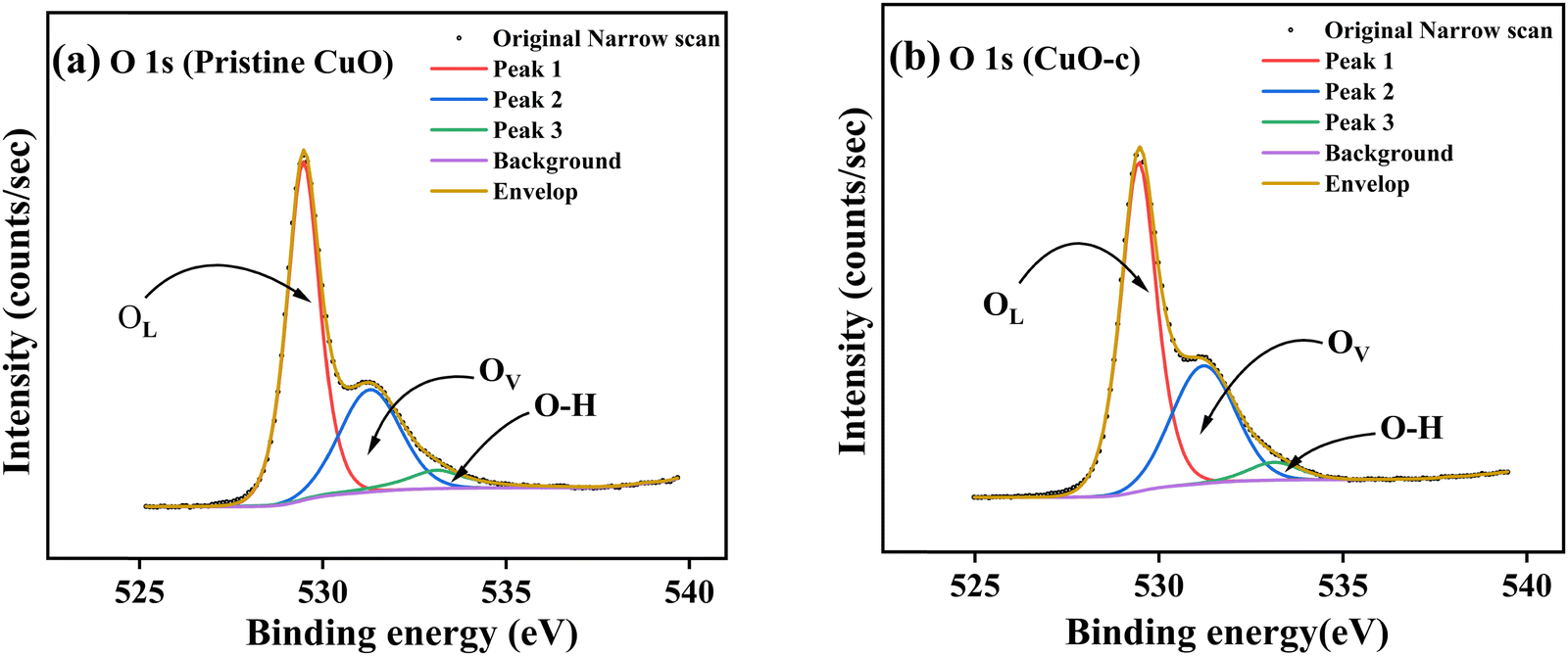 | ||
| Fig. 7 High-resolution spectra of (a) O 1s from pristine CuO and (b) O 1s from CuO-c, along with deconvolution. | ||
It has also been noted that doping CuO causes a little change in the binding energy of the O 1s spectrum (Fig. 7b). The peak intensities also vary somewhat from one another, most likely because of differences in the number of defects present at various doping levels. The O 1s spectrum of doped CuO-c shows a redshift at 529.4, 531, and 533.3 eV, respectively. The amounts of oxygen vacancies may be inferred from the intensity of the OV peak. We have compared the XPS spectra of the O 1s of CuO-c and pristine CuO to demonstrate the effect of doping on the concentration of oxygen vacancies. The oxygen-deficient area peak of the pristine CuO sample is much weaker than the peak of the CuO-c sample, as seen clearly from the figure. This finding is suggestive of an increase in oxygen vacancies in CuO as a consequence of effective doping element incorporation. Moreover, the relative concentration of oxygen vacancies (OV/O 1s) can be roughly semi-quantitative by its area ratio in the O 1s XPS curves. Consequently, the concentration of oxygen vacancies rises from 31.86% for pristine CuO to 35.33% for doped CuO-c according to the comparison of the high-resolution O 1s XPS spectra. These results indicate that doping may increase oxygen vacancies, which is beneficial for the development of ferromagnetic coupling and the enhancement of magnetism in CuO NCs.8
Therefore, a combination of research results, obtained via XRD and XPS methods, allows us to conclude that the obtained NCs are composed of copper oxide, and for doped NCs, chromium, iron, cobalt, nickel, and zinc atoms are likely to be included in the monoclinic crystal structure of copper oxide.
Surface morphology
Moreover, to further characterize the surface morphology, particle size distribution, inter-planar spacing, and type of constituent elements present in the NCs, techniques like field emission scanning electron microscopy (FE-SEM), high-resolution transmission electron microscopy (HR-TEM), and energy dispersive X-ray spectroscopy (EDS) elemental analysis were synergistically employed.The SEM images (as shown in Fig. 8a–d) support the formation of irregular polyhedron-shaped fused particles for these samples. This peculiar growth in the grains may be attributed to the uncontrolled aggregation of atoms on the lower energy lattice sites.45 Moreover, during the annealing of the samples, the formation of larger grains by the coalescence of smaller grains might occur, which would increase the size of the particles. It is also apparent from the SEM images that multi-granular structures with strong interconnections are porous. Such porous surface morphology can deliver a greater surface area, making it feasible for gas-sensing device applications and supercapacitor properties. Moreover, the lengths of the grains are found to be inhomogeneous, with a wide range of size distribution.
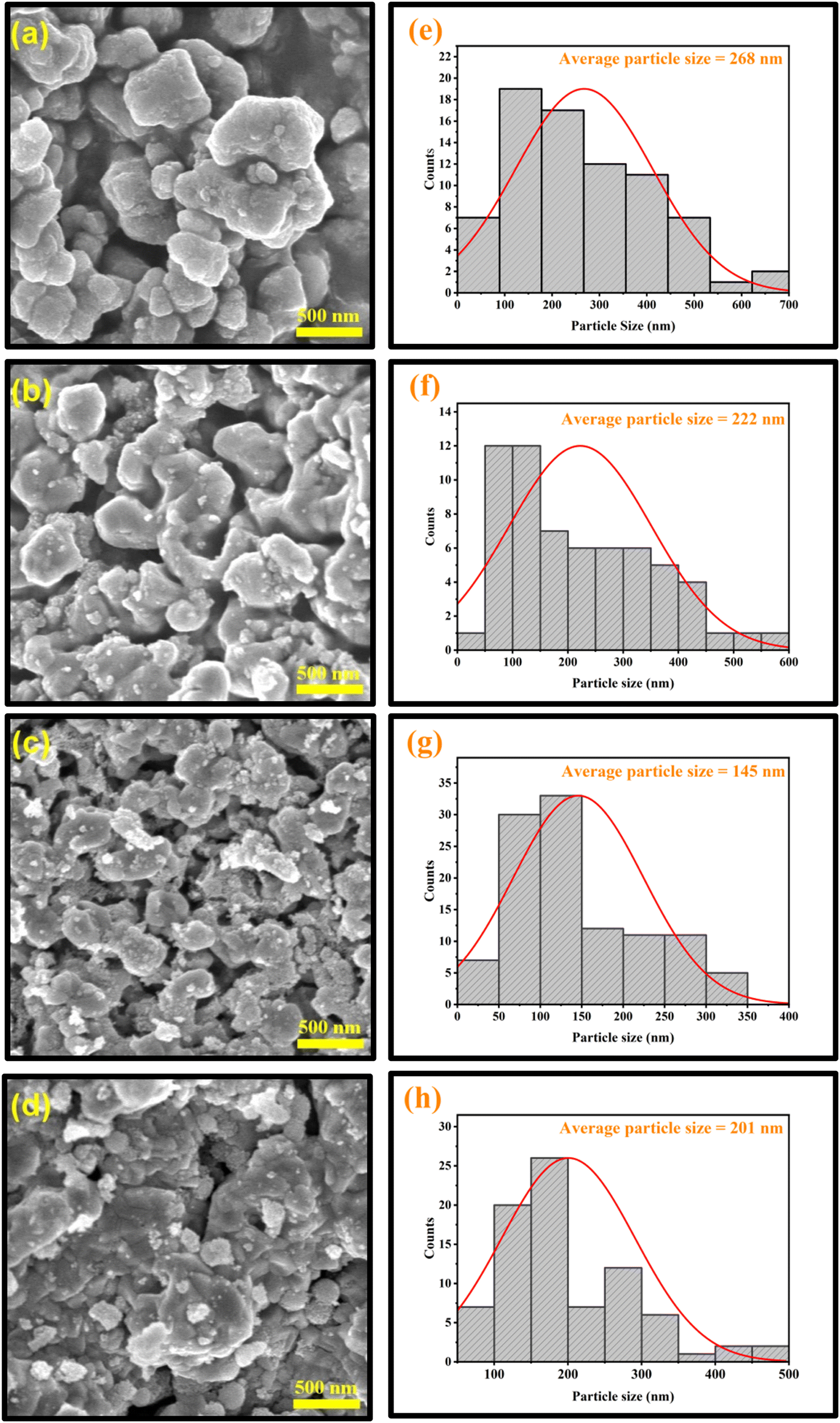 | ||
| Fig. 8 FE-SEM images of (a) pristine CuO, (b) CuO-a, (c) CuO-b, and (d) CuO-c, along with a histogram showing particle size distribution curves of (e) pristine CuO, (f) CuO-a, (g) CuO-b, and (h) CuO-c NCs. | ||
Doping has caused a significant alteration in the morphology of the prepared CuO particles. In some regions, the big particles were surrounded by smaller nanoparticles for the doped samples. Due to the agglomeration of these tiny particles, lump-like structures were formed. The lumping of powders may be due to moisture produced inside the samples.46 The particles are agglomerated from a few nm to a few μm. This agglomeration minimizes their surface free energy, which signifies the thermodynamically stable growth mechanism, resulting in an even more porous structure, as shown in Fig. 8c. Also, the surface appears to be rough. Distortion and discontinuity of the lattice may be caused by the different radii of the dopant ions and Cu2+, which can then lead to the suppression of grain growth. Therefore, when the concentration of the dopant increased up to CuO-b, the particle size dropped, which is in good accordance with the calculated crystallite size from XRD analysis (as shown in Table 1). However, another reason for this size reduction behavior could be the Zener pinning effect.47 According to this effect, vacancies and other flaws (whose presence is confirmed by XRD and XPS) in the CuO crystals exert an inhibiting force that limits their growth.48
These reductions in particle size with enhanced porosity provide a high volume-specific surface area for better ion intercalation, more electroactive sites, and enhancement of electrolyte access that gives desired electrochemical properties with improved efficiency in attaining higher capacitance. Hence, it is beneficial to employ these doped CuO NCs as the electrode material in order to gain a remarkable cycle ability and superior specific capacitance for supercapacitors.49 In addition, the increased surface area of the doped particles may also have a major impact on the optical and magnetic properties of the samples.50 However, a few particles displayed broken edges as a consequence of incomplete growth during synthesis. On further increasing the doping concentration, the particle size increases, which is analogous to the increase in crystallite size obtained from XRD analysis in the case of highly doped CuO-c NCs.
For all samples, average sizes were determined using a Gaussian fitted histogram in OriginPro software, which are depicted in Fig. 8e–h. In order to better understand the data, log-normal functions were fitted to the histograms. The fitted functions provided an average particle size of 268, 222, 145, and 201 nm for pristine CuO, CuO-a, CuO-b, and CuO-c samples, respectively. Since the size and surface area of sol–gel-derived CuO are crucial to achieving many of the desired physical characteristics in a wide range of applications (sensing, catalysis, etc.), the introduction of dopants into the synthesis process is very encouraging.51
The HR-TEM images of the synthesized NCs shown in Fig. 9 show the presence of ellipsoid-shaped nanocrystals, which are very thin and partially transparent. The HR-TEM images in Fig. 9a–d confirmed that each particle is the accumulation of ultra-small nanoclusters of single crystals after nanocrystal deposition and growth. Hence, very few single crystals are completely separated. This confirms that the actual sizes of these synthesized NCs are very small compared to those measured from SEM images. These nanocrystals also have a tendency to form amorphous boundaries at the junction of the clusters. This phenomenon may be linked to the variation in structural disorder and microstrain induced in the host CuO matrix.
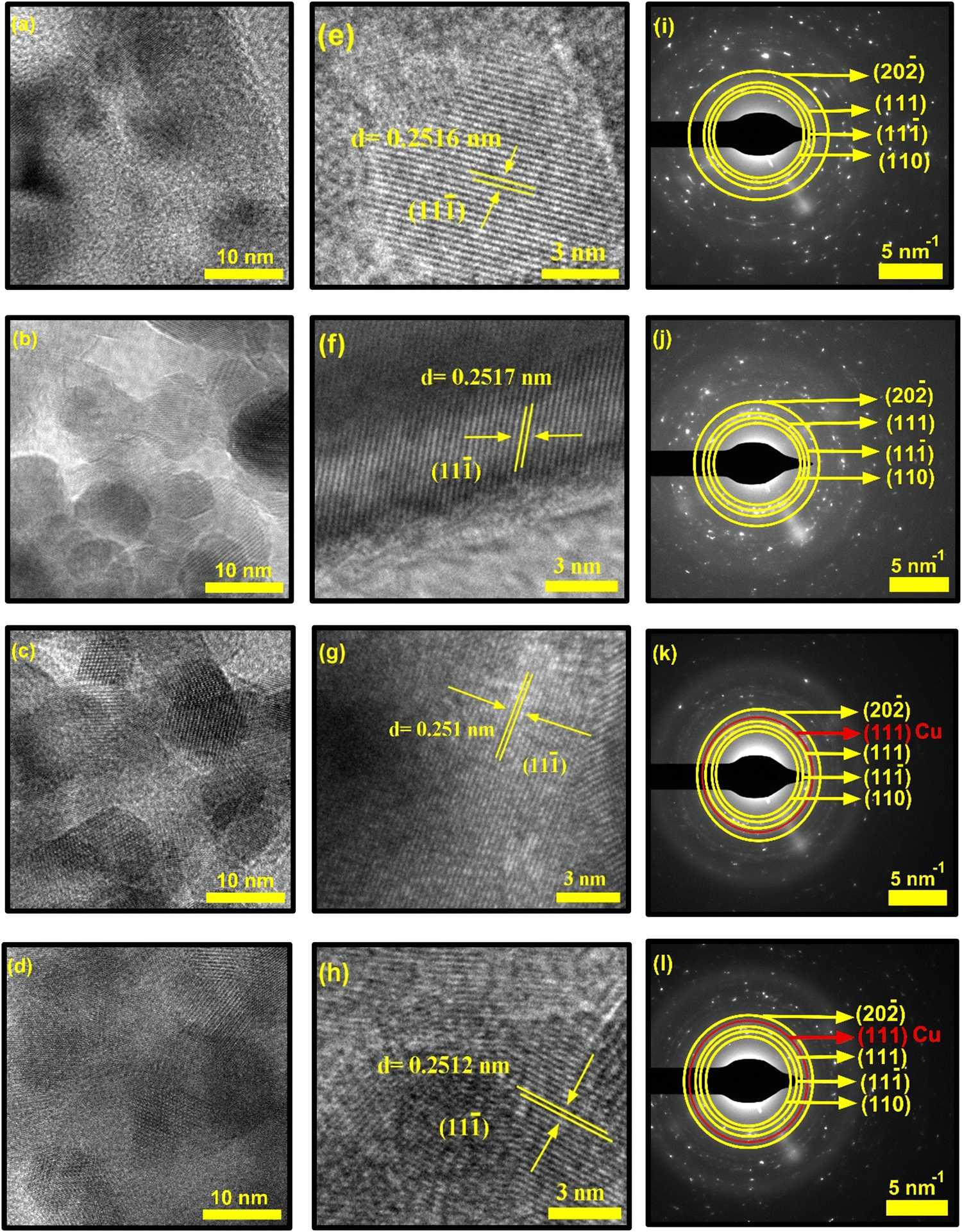 | ||
| Fig. 9 (a)–(d) HR-TEM images of pristine CuO, CuO-a, CuO-b, and CuO-c NCs showing the formation of nanocrystals, (e)–(h) images showing lattice fringes, and (i)–(l) the corresponding SAED patterns of NCs. | ||
Although the nanocrystals were highly agglomerated and overlapping of crystal fringes occurred due to this high agglomeration, the lattice fringes of some polycrystalline CuO NCs were visible at higher magnification, which are shown in Fig. 9e–h. Fig. 9e presents the calculated interplanar distances of pristine CuO, where the lattice spacing of 0.2516 nm belongs to the (11−1) diffraction planes of monoclinic CuO, indicating preferential growth of these nanocrystals along the [11−1] crystal axis. The calculated values of the doped samples corresponding to the (11−1) plane are 0.2517 nm for CuO-a, 0.251 nm for CuO-b, and 0.2512 nm for CuO-c samples. It should be noted that these observations are in considerable accordance with the XRD results (as tabulated in Table 1). The slightly large interlayer spacing of CuO and CuO-a provides easy diffusion of the electrolyte.52
The crystallinity of the prepared CuO NCs that was previously discussed in the XRD analysis can also be confirmed by the selected area electron diffraction (SAED) pattern of the TEM analysis (as shown in Fig. 9i–l). The polycrystalline nature of the CuO NCs is confirmed by their appearance as concentric rings made up of bright spots with varying orientations. The ImageJ tool was used to determine the diameter of the rings, and the resulting d-spacing values were analyzed. The interplanar distances of pristine CuO NCs, found at d1 = 0.278 nm, d2 = 0.253 nm, d3 = 0.232 nm, and d4 = 0.1866 nm, can be indexed to crystal planes (110), (11−1), (111), and (−202), respectively. This indexing of the SAED pattern corresponding to (110), (11−1), (111), and (−202) planes is consistent with the XRD analysis and the matched JCPDS card number. Thus, the SAED pattern confirms the successful synthesis of tenorite C2/c symmetric CuO NCs. Moreover, for doped CuO-b and CuO-c, an extra ring at an interplanar distance of d = 0.208 and d = 0.21 nm, respectively, indicates the presence of the Cu (111) plane. Misorientation of the fundamental crystallographic domains is indicated by the elongation of several diffraction spots in the diffraction patterns.53 Thus, it can be concluded that doping plays a critical role in altering the morphology of pristine CuO NCs.
The EDX analysis was performed to study the types of elements present in the samples. The elemental analysis results (Fig. S3, ESI†) indicate the presence of Cu and O in pristine CuO. The spectra showed no impurity peaks other than the C peak (due to surface contamination during TEM analysis), which further confirms that the as-prepared nanocrystals are freed from impurities that can emerge from the initial precursors, like nitrogen. For doped samples, the EDX spectral analysis confirmed the presence of Cr, Fe, Co, Ni, Cu, Zn, and O atoms. Hence, dopant incorporation into the structure is confirmed.
The optical properties of pristine CuO and doped CuO NCs were analyzed using diffuse reflectance spectroscopy (DRS) to find the application boundaries of synthesized samples in various fields like photodetectors, photocatalysis, photovoltaics, pollutant removal systems, and energy storage devices.9 The DRS spectra were recorded in the wavelength range of 400–1000 nm at room temperature to predict the energy band structure. Fig. 10a shows the relative amount of reflected light from the samples using reflectance spectra. The reflectance spectra show only around 10% reflectivity in the visible and ultra-violet regions, which justifies the black appearance of the synthesized NCs in sunlight.54 In addition, the observed high infrared reflection can be attributed to the plasmon resonance of NCs.55
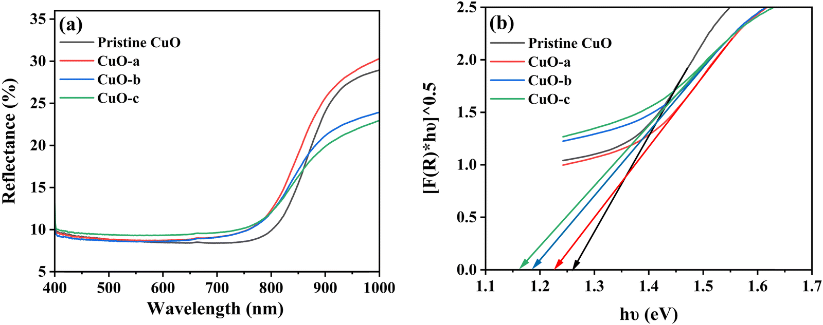 | ||
| Fig. 10 (a) Reflectance vs. wavelength spectra and (b) indirect band gaps of pristine and doped CuO NCs. | ||
To study the absorption characteristics of nanocrystals, the reflectance spectra were converted into the absorbance mode using the Kubelka–Munk function (F(R)) using the following equation:56
 | (11) |
| F(R)hυ = A(hυ − Eg)n | (12) |
| Samples | Absorption edge (nm) | Bandgap (eV) | Refractive index (n) | Dielectric constant (ε∞) |
|---|---|---|---|---|
| Pristine CuO | 984.69 | 1.26 | 3.09 | 9.55 |
| CuO-a | 1008.71 | 1.23 | 3.10 | 9.61 |
| CuO-b | 1042.61 | 1.19 | 3.13 | 9.80 |
| CuO-c | 1069.58 | 1.16 | 3.15 | 9.92 |
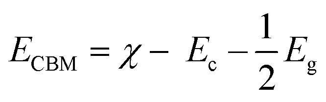
The calculated indirect band gap energy (the electron momentum is not conserved in the transition) for pristine CuO is 1.26 eV, which is notably lower than the previously stated values for undoped CuO.3 The electronic transition from the hybridized O-2p valence band to the Cu-3d conduction band provides a measure of the band gap in undoped CuO. However, in this study, the lower bandgap values of pristine CuO can be attributed to the presence of surface oxygen vacancy states, as observed in XPS. The surface oxygen vacancies can narrow the bandgap for metal oxides and downshift both the VB and CB, indicating higher wavelength adsorption leading to better utilization of the solar spectrum and thermodynamically favorable conditions towards water oxidation (as depicted in Fig. 11) due to the decrease in overpotential associated with this reaction.57,58 Hence, this material is suitable for energy harvesting applications such as sunlight-driven oxygen generation from water.59,60 The photocatalytic potential of pristine CuO NCs was investigated by determining their valence band maximum (VBM) and conduction band minimum (CBM) with the use of the Mulliken electronegativity approach.61 According to this formula,
 | (13) |
| EVBM = ECBM + Eg | (14) |
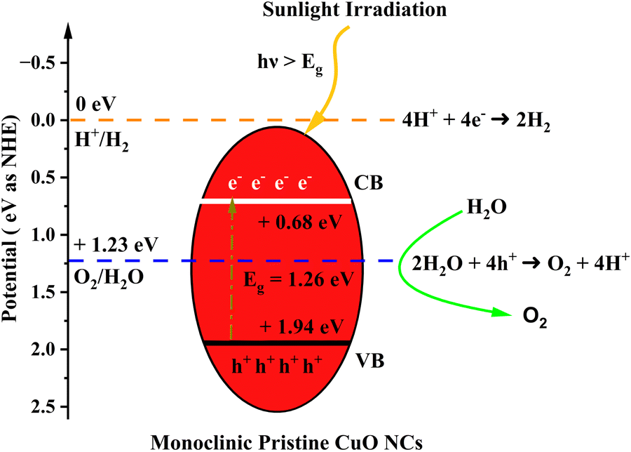 | ||
| Fig. 11 Schematic diagram of the calculated band edge position with respect to the H+/H2 potential and O2/H2O potential. | ||
The bandgap values of doped CuO are 1.23, 1.19, and 1.16 eV for CuO-a, CuO-b, and CuO-c NCs, respectively. Thus, it is found that the optical bandgap is gradually decreased with doping concentration. The bandgap tailoring effect, caused by the existence of copper vacancy defects along with oxygen vacancies (as shown in defect reaction equations in eqn (1) and (2), may be responsible for this decrease in the energy band gap from 1.26 to 1.16 eV. Furthermore, dopants are expected to have a low degree of hybridization for a stable electronic configuration, which in turn may lead to the creation of a unique energy level in between Cu 3d and O 2p, resulting in a narrowed band gap.64 Therefore, the absorption edge is redshifted as a result of the electrical transition from the valence band to the dopant level and subsequently from the dopant level to the conduction band. Another factor that may contribute to bandgap narrowing is the presence of a localized t2g state of the doping element, which can be found in the center of the band gap (when Cr or Fe is used as the dopant) or at the top of the valence band (when Co is used as the dopant).65 Hence, it can be deduced that the band gap values in the doped CuO NCs dropped because the electrical transition between the CB and VB was disrupted by the creation of a number of defect energy bands in the presence of dopants. The absorption edge of pristine and doped CuO NCs was estimated using the equation:66 , where h is the Planck constant and c is the speed of light. Strong absorption in the visible region and a continuous redshift with an increase in the concentration of dopants are confirmed by the absorption edge values. The absorption edge along with the band gap of the pristine and doped CuO nanocrystals are listed in Table 2. The increasing redshift also indicates that surface defects are likely to blame for the intra-gap state effects.67 Moreover, the higher visible absorption achieved for the doped NCs leads to higher application efficiency. Entrapment of carriers (e−/h+) occurs because dopant impurities act as trap centers. Carrier entrapment is a phenomenon that may reduce the recombination rate even when the carrier density and quantum efficiency are both increased. This suggests doped CuO NCs might be used in solar cell technology.68 Also, doped NCs have improved degradation performance (Fig. 12) because the narrowed bandgap allows for more absorption of infrared and visible light at a lower recombination rate. When exposed to sunlight, electrons in the valence band transit to the conduction band, creating electron/hole (e−–h+) pairs. By oxidizing water molecules close to the surface, the hole creates hydroxyl radicals (˙OH), and an electron collides with oxygen molecules to create superoxide radicals (˙O2−). The organic contaminants in the water were oxidized and broken down by these free radicals. The response mechanism is as follows:
| ˙O2− + ˙OH + Organic contaminants → Degradation products | (15) |
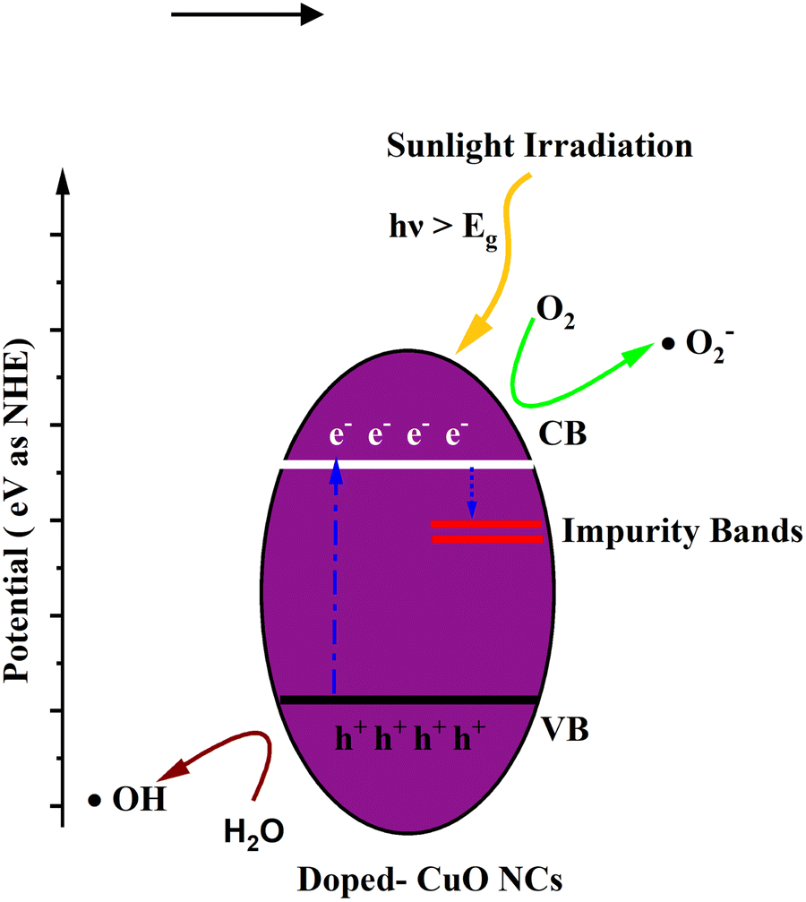 | ||
| Fig. 12 Schematic diagram depicting the photocatalysis reaction mechanism of doped CuO NCs. | ||
Photogenerated electrons are trapped in the impurity band, lowering the rate of electron–hole recombination, enhancing the mean lifetime of electrons.69 As the photo-generated charge carriers migrate to the surface of the nanostructured particles and the oxidation process takes place there, the particle surface area also plays an important role in photocatalysis.70,71 Photocatalysis is enhanced when the particle size of NCs is reduced (due to dopants), since this allows more pollutant molecules to approach the catalyst surface. Moreover, the existence of abundant surface valence states and defects for doped NCs (as shown in Fig. 6) can improve the intrinsic activity of the doped CuO samples.72 However, heavy doping could have been able to fine-tune the optical characteristics further by forming recombination centers due to the delocalization of the carriers, as confirmed by the formation of the secondary Cu phase mentioned in XRD and XPS analyses.
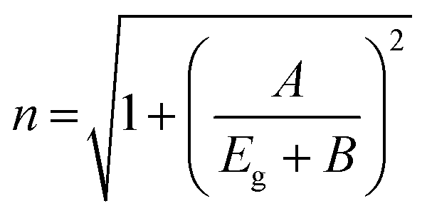
Important factors for integrated optoelectronic devices are the refractive index and dielectric constant of the synthesized nanocrystals. The degree to which a semiconductor transmits incident spectrum radiation is indicated by its refractive index. The Herve and Vandamme relation was used to determine the refractive index (n) of the synthesized materials from the bandgap values as follows:
 | (16) |
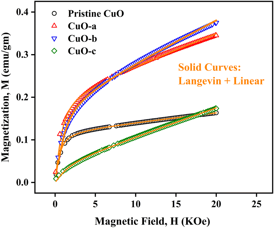
To study the magnetic properties, field-dependent magnetization (M) versus magnetic field (H) curves of the synthesized CuO NCs are displayed in Fig. 13a. The M–H curves obtained at 300 K show narrow magnetic hysteresis loops, indicating a typical weak ferromagnetic nature at lower fields where magnetization does not reach the saturation value even up to the maximum applied magnetic field. This non-saturation and linear behavior in the samples indicate the presence of paramagnetism. If the susceptibility of the paramagnetic (PM) component is known, the contributions of paramagnetism and ferromagnetism can be distinguished. In line with earlier literature, we selected a simple method for calculating the susceptibility of the PM component by calculating the tangent of the top curve (the demagnetizing curve) of the M–H loop at the highest applied field.68 When the PM contribution is subtracted from the total response, all the samples represent S-like curves, showing room-temperature ferromagnetic characteristics. FM and PM components are shown separately in Fig. 13b and c. It is possible that the matrix of NCs is responsible for this paramagnetic component seen in the room temperature M–H curves of CuO samples.76 As depicted in Fig. 13c, PM interaction is highest for the CuO-b sample and lowest for the pristine CuO sample, with similar contributions for the CuO-a and CuO-c samples. This difference in PM interaction with doping concentration can be attributed to the different magnetic transition temperatures for random flips of the magnetic moments present in the matrix, which is shown in Fig. S4 (ESI†) as the relationship between magnetization (M) and temperature (T). With a transition temperature of just 40.1 K, CuO-b initiates paramagnetism at a substantially lower temperature than other NCs, which can be attributed to the greater PM contribution reported at RT for CuO-b.77 This low transition temperature of CuO-b NCs can be attributed to the smallest crystallite size of 21.8 nm compared to other NCs.78 Moreover, the low transition temperature of CuO-b enhances its potential to be used in magnetic hyperthermia.79 The identical contribution of paramagnetism may be explained by the comparable transition temperature of 110.02 K for CuO-a and CuO-c. Hence, the M–T curves confirm that the linear portion of the M–H curves is coming from the presence of paramagnetism in the matrix at RT. As a result, changes in the composition and grain size might affect the coupling between magnetic moments, leading to a modification of the transition temperature.
 | ||
| Fig. 13 (a) M–H hysteresis curves of CuO NCs measured at room temperature, (b) ferromagnetic contribution of NCs and (c) paramagnetic contribution of NCs. | ||
The saturation magnetization (Ms), remanent magnetization (Mr), squareness ratio (S = Mr/Ms), and coercive field (Hc) are calculated using the hysteresis loops and tabulated in Table 3. The coercivity value of pristine CuO is 69.7 Oe. Upon enhancing the doping concentration from pristine CuO to CuO-b, the coercivity has been on the rise, from 69.7 Oe to 189.08 Oe. Coercivity drops to 55.5 Oe if the doping concentration is increased further (for CuO-c). Coercivity is an indicator of the strength of a magnetic field necessary to overcome the energy of magnetic anisotropy. Since the current samples have little magnetic anisotropy, as noticed by their tiny hysteresis loop, their ferromagnetism is rather pliable.80 The smaller crystallite size of CuO-b usually results in relatively large exchange coupling, J, which is taking place between the core and the surface of the NCs and can be attributed to this larger coercivity.81 High coercivity plays a vital role in biomedical applications.82
| Samples | Coercivity, Hc (Oe) | Saturation magnetization, Ms (emu gm−1) | Remanent magnetization, Mr (emu gm−1) | Squareness (Mr/Ms) | M o (emu gm−1) | Susceptibility, χm × 10−6 (emu gm−1 Oe) | m eff × 10−17 (emu) | N × 1015 (cm3) |
|---|---|---|---|---|---|---|---|---|
| Pristine CuO | 69.7 | 0.1154 | 0.004 | 0.034 | 0.1212 | 2.2 | 13.9 | 0.87 |
| CuO-a | 107.7 | 0.2081 | 0.009 | 0.043 | 0.2056 | 7.41 | 9.87 | 2.08 |
| CuO-b | 189.08 | 0.1946 | 0.012 | 0.062 | 0.1914 | 9.73 | 6.99 | 2.74 |
| CuO-c | 55.5 | 0.0412 | 0.002 | 0.049 | 0.0415 | 6.77 | 5.36 | 0.77 |
Saturation magnetizations were measured to be 0.1154 emu gm−1 for pristine CuO, 0.2081 emu gm−1 for CuO-a NCs, 0.1946 emu gm−1 for CuO-b NCs, and 0.0412 emu gm−1 for CuO-c NCs. In addition, pristine CuO NCs had a remanent magnetization of 0.004 emu gm−1; CuO-a NCs had a remanent magnetization of 0.009 emu gm−1; CuO-b NCs had a remanent magnetization of 0.012 emu gm−1; and CuO-c NCs had a remanent magnetization of 0.002 emu gm−1. These changes in remanent magnetization with doping concentration are involved in domain wall motion.83 Due to this low retentivity, all the samples are defined as magnetically clean materials. The decrease in retentivity to a lower value even than the pristine CuO NCs for CuO-c suggests that CuO NCs can be used for the data storage application. As a measure of its ferromagnetic strength, pristine CuO has a squareness value (squareness of the hysteresis loop) of 0.034. There seems to be a gradual change from a soft magnet to a hard magnet and back to a soft magnet, as the squareness values initially increased to 0.043 and 0.062 for CuO-a and CuO-b, respectively, before decreasing to 0.049 for CuO-c NCs. Hence, doping in CuO can be used as a regulator for the magnetic nature of CuO NCs (Fig. 13a).
 | ||
| Fig. 14 Fitted M–H curves of (a) pristine and (b) and (d) doped CuO NCs using the BMP model. | ||
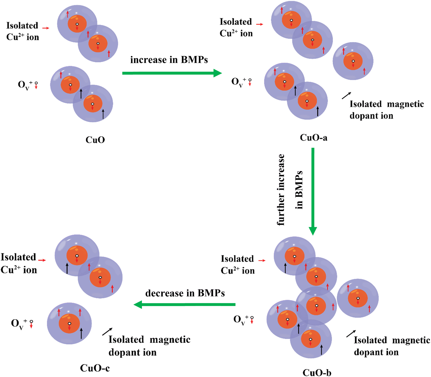
The Ruderman–Kittel–Kasuya–Yoshida (RKKY) and bound magnetic polaron (BMP) models are two of the most popular theories used to explain the RTFM.84 Free conduction band electrons are involved in RKKY interactions, and CuO cannot transform from a semiconductor into a metal at such a low doping concentration. This means that DMSs, such as resistive CuO systems, are not a good match for the RKKY model.85 However, XPS measurements and defect reactions demonstrate the presence of point defects such as oxygen vacancies and host lattice cation vacancies in the present samples, suggesting that these point defects can efficiently mediate intrinsic ferromagnetism. The BMP model provides a satisfactory explanation for the ferromagnetic process generated by these defects. Bound magnetic polarons (BMPs), which are considered as an isolated ferromagnetic identity, create orbits with a finite diameter that are similar to those of a hydrogenic Bohr orbit due to the localization of the electrons in the defect centers.86 Thus, depending on the cation interaction with vacancies, magnetism could occur in the CuO NCs via the cation–defect center–cation configuration. By breaking chemical bonds due to heat evaporation, oxygen atoms may escape from lattice locations during the annealing of sol–gel-derived CuO NCs, creating oxygen vacancies. Further, due to air annealing, some vacancies will be filled. This two-contrasting phenomenon leads to an optimum oxygen vacancy concentration. In pristine CuO, electrons released by oxygen vacancies may be “trapped” by Cu2+ ions, leading to the formation of an ionized vacancy (Ov+) state. The s–d exchange interaction among the spin of the 1s1 electron of the Ov+ state and the 3d9 electron of the Cu2+ ions favors long-range FM ordering. At room temperature, a long-range ferromagnetic order is created when BMPs overlap, aligning Cu2+ spins (as shown in Fig. 15).
 | ||
| Fig. 15 Schematic representation of the evolution of the oxygen defect-mediated BMP model with increasing dosage of the dopant. | ||
The influence of doping magnetic (Cr3+, Fe3+, Co2+, and Ni2+) and non-magnetic (Zn2+) cations in CuO NCs on the evolution of FM characteristics with varying doping concentrations is also analyzed in the present study. These additional magnetic and non-magnetic impurities can enhance oxygen vacancies during annealing, as confirmed by the XPS result of CuO-c. Also, the exchange interaction between Cu2+ and magnetic cations at the surface in the presence of a carrier in the Ov+ state presents a high ferromagnetic coupling energy, even at larger distances. According to some researchers, cation vacancies were also found to contribute to the intrinsic exchange interactions in the DMS system through BMP production, in addition to the oxygen vacancies.87 Therefore, RTFM in doped CuO may also be generated due to the exchange interaction between dopants mediated by Cu vacancies (formed due to the substitution by Fe3+ and Cr3+). In addition to the Cu 3d orbitals and the oxygen vacancies, the O 2p orbitals that originate from the Cu site vacancy may also be supportive of magnetic ordering.88
Moreover, BMPs can also be used to explain the features of M–H curves. The unsaturation nature indicates that BMP concentrations are below the percolation threshold that is required for bulk ferromagnetism; as for the inner region of the NCs, BMPs cannot be formed due to a lack of oxygen vacancies. Each BMP has a significant net spontaneous magnetic moment that aligns rapidly in a magnetic field, leading to a rapid increase in M even at weak H fields, as the d spins in the matrix outside the BMP align only slowly with the H field. Paramagnetically interacting d-spins in the matrix at RT result in a considerably lower moment per d-spin than the BMP. Hence, only at higher fields, the magnetic contribution from the paramagnetically aligned Cu2+ of the core is dominant, which ultimately leads to a paramagnetic tail in the samples.
The BMP model was also used to perform a quantitative study of the magnetization curves by isolating the contribution of the BMPs from that of the PM matrix, determining the true spontaneous moment ms of a single BMP, and calculating the number of BMPs per cm3 (N). In the BMP model, ferromagnetic nature may be satisfactorily explained using the Langevin profile:
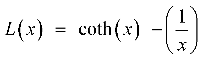 | (17) |
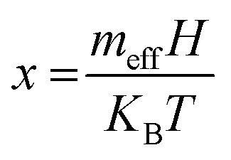 ; meff is the effective magnetic moment per BMP and KB is Boltzmann's constant.89 This FM part may be written in terms of the saturation magnetization, M0, as MFM = M0L(x) where the value of M0 is the product of N and ms. A single BMP's aligned moment has the same magnitude as the true spontaneous moment, ms. The rate at which the true moment aligns along H is, however, controlled by the effective moment meff in the Langevin function's argument. There is no distinction between ms and meff, and the magnetization of BMPs in the collective regime was modeled using meff = ms. Moreover, in the high field regime, the existence of the matrix PM component can be expressed in terms of the PM susceptibility χPM as MPM = χPMH. Hence, the following equation was used to fit the overall magnetization data from the M–H curves:
| M = MFM + MPM | (18) |
| M = M0L(x) + χmH | (19) |
As noticed from Table 3, the number of BMPs is changing since we are varying the number of donors and magnetic defects. An increased FM in CuO-a and CuO-b indicates the formation of more BMPs through an increase in cation and oxygen vacancies. Electrons trapped in OV+ induce spin orientation for the adjacent dopants, forming a ferromagnetic coupling of the magnetic cation–OV+–magnetic cation. Thus, doping may increase the number of BMPs by increasing the number of defect centers. However, the suppression of BMPs in CuO-c, even in the presence of magnetic impurities and vacancies (as confirmed by XPS), results in a reduction of FM behavior. This suppression of BMPs can be attributed to the delocalization of carriers from the bound polarons due to the increasing mobility of charge carriers at higher carrier concentrations. Thus, it breaks the fundamental structure of polarons. In the present study, XRD and XPS analyses ensure the presence of a secondary Cu phase in CuO-c, which confirms the delocalization of bound electrons between metallic Cu and oxygen vacancies at this higher doping, which were previously localized or trapped. Thus, the defect reaction equation (eqn (4)) can be rewritten more accurately as
| Cu2+ + 2e′′ (delocalized) → Cu (metal) | (20) |
Another phenomenon observed from the fitting data is the decrease in effective magnetic moment per BMP (meff) with increasing concentrations of dopants, which in turn decreases saturation magnetization (Ms). This variation in Msversus doping concentration can be attributed to the overlapping of BMPs, as due to overlapping each magnetic moment is shared between two or more polarons, dividing its magnetization effect among the overlapped polarons. Moreover, in doped NCs, the extra dopants can be located in the O2− lattice of the tenorite structure, forming an antiferromagnetic coupling of the magnetic ion–O2−–magnetic ion, which may drastically cut down on the ’magnetic moments of polarons. Also, substitution of Cu2+ ions by non-magnetic Zn2+ reduces the number of exchange interactions inside the polarons as Zn2+ is diamagnetic in nature. Hence, the combination of these factors reduces the effective magnetic moment per BMP (meff) to a greater extent, which becomes more prominent with increasing doping concentration. This also explains the decrease in saturation magnetization for CuO-b (as noticed in Fig. 13b). Despite the presence of a higher number of polarons, the saturation magnetism is less than that in the CuO-a sample because of this reduction in meff, as saturation magnetization is the product of the number of polarons per cm3 and the spontaneous magnetic moment per polaron. Together, our results provide evidence that the dopant plays a significant role in the magnetic moments of CuO NCs and reinforce the relevance of the BMP model in understanding the underlying mechanism responsible for the ferromagnetism of dilute magnetic semiconductors.
Based on the defect reactions, XPS analysis, and values generated from fitting the BMP model, a schematic representation of the BMP model is created, as shown in Fig. 15. In addition to the magnetic polarons, the CuO matrix also contains some randomly distributed isolated ions. It has been shown that oxygen vacancies (Ov) are the most dominant defects in CuO. Neighboring BMPs overlap and interact with one another via the Ov+ site when the concentration of localized oxygen vacancies rises.
Conclusions
Modified sol–gel-derived pristine and doped CuO nanocrystals have been studied to correlate the evolution of structural, morphological, optical, and magnetic properties with defect modulation. The coexistence of two phases corresponding to CuO and metallic Cu for higher doping concentrations is confirmed by their associated Bragg positions in the fitted Rietveld refined curves. Due to charge variation, copper vacancies increase when Fe3+ and Cr3+ ions are used to substitute Cu2+ ions. XPS confirms the presence of impurity ions, which are responsible for the defect mechanisms. Reflectance spectroscopy revealed the promising potential of pristine CuO NCs in photocatalytic O2 evolution from water due to their advantageous valence band position. A clear redshift was evident in the absorption edge of the doped nanostructures due to the impurity bands introduced via doping, which favor visible light photoactivity. The mechanism behind RTFM below the percolation threshold in both pristine and doped CuO materials has been explained based on the overlapping of defect-induced bound magnetic polarons (BMPs). Both the oxygen vacancy and cationic vacancy defects are separately capable of producing BMPs. As the additional magnetic and non-magnetic impurities introduce both oxygen and cationic vacancies, doping up to a certain concentration effectively boosts BMP formation by creating more cation–defect–cation coupling. However, increasing carrier mobility further decreases the concentration of BMPs, despite having enough defects and magnetic ions. These findings are essential for spintronic devices because they provide insight into the inherent magnetic nature of DMSs and offer directions for manipulating their magnetic characteristics at ambient temperature. In conclusion, we identified the most critical parameters, such as doping concentration and the dopant number, that contribute to the creation of interesting defect chemistry to regulate the performance of DMSs in spintronics, photonics, catalytic applications, etc.Conflicts of interest
There are no conflicts to declare.Acknowledgements
The authors would like to express their gratitude to the Research and Innovation Centre for Science and Engineering (RISE), Bangladesh University of Engineering and Technology (BUET), Dhaka-1000, Bangladesh for funding through the RISE Internal Research Grant. The authors would also like to express their appreciation to Materials science division, Atomic Energy Centre, Dhaka, for their assistance with nanoparticles characterization.References
- B. Mondal and P. K. Gogoi, Nanoscale Heterostructured Materials Based on Metal Oxides for a Chemiresistive Gas Sensor, ACS Appl. Electron. Mater., 2022, 4(1), 59–86, DOI:10.1021/acsaelm.1c00841.
- V. Senthilkumar, Y. S. Kim, S. Chandrasekaran, B. Rajagopalan, E. J. Kim and J. S. Chung, Comparative Supercapacitance Performance of CuO Nanostructures for Energy Storage Device Applications, RSC Adv., 2015, 5(26), 20545–20553, 10.1039/C5RA00035A.
- S. V. Gupta, V. V. Kulkarni and M. Ahmaruzzaman, Bandgap Engineering Approach for Designing CuO/Mn3O4/CeO2 Heterojunction as a Novel Photocatalyst for AOP-Assisted Degradation of Malachite Green Dye, Sci. Rep., 2023, 13(1), 3009, DOI:10.1038/s41598-023-30096-y.
- E. Kan, M. Li, S. Hu, C. Xiao, H. Xiang and K. Deng, Two-Dimensional Hexagonal Transition-Metal Oxide for Spintronics, J. Phys. Chem. Lett., 2013, 4(7), 1120–1125, DOI:10.1021/jz4000559.
- M. Shahmiri, S. Bayat and S. Kharrazi, Catalytic Performance of PVP-Coated CuO Nanosheets under Environmentally Friendly Conditions, RSC Adv., 2023, 13(19), 13213–13223, 10.1039/D2RA07645D.
- A. Alsulmi, N. N. Mohammed, A. Soltan, M. F. A. Messih and M. A. Ahmed, Engineering S-Scheme CuO/ZnO Heterojunctions Sonochemically for Eradicating RhB Dye from Wastewater under Solar Radiation, RSC Adv., 2023, 13(19), 13269–13281, 10.1039/D3RA00924F.
- Y.-S. Lai, D.-J. Huang, X.-X. Zhang and Y.-H. Su, Spintronic Filter via p-Typed Polaron State in Photoelectron Conversion Integrating Devices. Sustain, Energy Fuels, 2023, 7(16), 3993–4001, 10.1039/D3SE00641G.
- M. Jamal, M. M. Billah and S. A. Ayon, Opto-Structural and Magnetic Properties of Fluorine Doped CuO Nanoparticles: An Experimental Study, Ceram. Int., 2023, 49(6), 10107–10118, DOI:10.1016/j.ceramint.2022.11.194.
- Q. Zhang, K. Zhang, D. Xu, G. Yang, H. Huang, F. Nie, C. Liu and S. Yang, CuO Nanostructures: Synthesis, Characterization, Growth Mechanisms, Fundamental Properties, and Applications, Prog. Mater. Sci., 2014, 60, 208–337, DOI:10.1016/j.pmatsci.2013.09.003.
- A. C. Nogueira, L. E. Gomes, J. A. P. Ferencz, J. E. F. S. Rodrigues, R. V. Gonçalves and H. Wender, Improved Visible Light Photoactivity of CuBi 2 O 4/CuO Heterojunctions for Photodegradation of Methylene Blue and Metronidazole, J. Phys. Chem. C, 2019, 123(42), 25680–25690, DOI:10.1021/acs.jpcc.9b06907.
- M. Kaur, A. Tovstolytkin and G. S. Lotey, Magnetoelectric Coupling in CuO Nanoparticles for Spintronics Applications, Electron. Mater. Lett., 2018, 14(3), 370–375, DOI:10.1007/s13391-018-0026-1.
- S. Baturay, I. Candan and C. Ozaydın, Structural, Optical, and Electrical Characterizations of Cr-Doped CuO Thin Films, J. Mater. Sci. Mater. Electron., 2022, 33(9), 7275–7287, DOI:10.1007/s10854-022-07918-2.
- P. Lu, P. Wu, J. Wang and X. Ma, Effect of Structure Distortion and Copper Vacancy on Ferromagnetism in Hydrothermally Synthesized CuO with Aliovalent Cr3+ Doping, Chem. Phys. Lett., 2019, 730, 297–301, DOI:10.1016/j.cplett.2019.06.029.
- S. P. Kamble and V. D. Mote, Structural, Optical and Magnetic Properties of Co Doped CuO Nano-Particles by Sol-Gel Auto Combustion Technique, Solid State Sci., 2019, 95, 105936, DOI:10.1016/j.solidstatesciences.2019.105936.
- M. M. Abrar, A. Kabir and S. S. Nishat, A DFT + U Study on the Structural, Electronic, Magnetic, and Optical Properties of Fe and Co Co-Doped CuO, Mater. Today Commun., 2022, 32, 103923, DOI:10.1016/j.mtcomm.2022.103923.
- C. Thangamani, M. Ponnar, P. Priyadharshini, P. Monisha, S. S. Gomathi and K. Pushpanathan, Magnetic behavior of ni-doped cuo nanoparticles synthesized by microwave irradiation method, Surf. Rev. Lett., 2019, 26(05), 1850184, DOI:10.1142/S0218625X18501846.
- J. Iqbal, T. Jan, S. Ul-Hassan, I. Ahmed, Q. Mansoor, M. Umair Ali, F. Abbas and M. Ismail, Facile Synthesis of Zn Doped CuO Hierarchical Nanostructures: Structural, Optical and Antibacterial Properties, AIP Adv., 2015, 5(12), 127112, DOI:10.1063/1.4937907.
- K. Rajendran, J. Yadav, T. S. Khan, M. A. Haider, S. Gupta and D. Jagadeesan, Oxygen Vacancy-Mediated Reactivity: The Curious Case of Reduction of Nitroquinoline to Aminoquinoline by CuO, J. Phys. Chem. C, 2023, 127(18), 8576–8584, DOI:10.1021/acs.jpcc.3c01374.
- G. Qiu, S. Dharmarathna, Y. Zhang, N. Opembe, H. Huang and S. L. Suib, Facile Microwave-Assisted Hydrothermal Synthesis of CuO Nanomaterials and Their Catalytic and Electrochemical Properties, J. Phys. Chem. C, 2012, 116(1), 468–477, DOI:10.1021/jp209911k.
- X. Zhang, G. Wang, X. Liu, J. Wu, M. Li, J. Gu, H. Liu and B. Fang, Different CuO Nanostructures: Synthesis, Characterization, and Applications for Glucose Sensors, J. Phys. Chem. C, 2008, 112(43), 16845–16849, DOI:10.1021/jp806985k.
- N. Kumar, S. S. Parui, S. Limbu, D. K. Mahato, N. Tiwari and R. N. Chauhan, Structural and Optical Properties of Sol–Gel Derived CuO and Cu2O Nanoparticles, Mater. Today Proc., 2021, 41, 237–241, DOI:10.1016/j.matpr.2020.08.800.
- S. P. Selvaraj, Enhanced Surface Morphology of Copper Oxide (CuO) Nanoparticles and Its Antibacterial Activities, Mater. Today Proc., 2022, 50, 2865–2868, DOI:10.1016/j.matpr.2020.09.574.
- R. D. Shannon, Revised Effective Ionic Radii and Systematic Studies of Interatomic Distances in Halides and Chalcogenides, Acta Crystallogr. Sect. A, 1976, 32(5), 751–767, DOI:10.1107/S0567739476001551.
- G. Nagaraju, Y. H. Ko and J. S. Yu, Self-Assembled Hierarchical β-Cobalt Hydroxide Nanostructures on Conductive Textiles by One-Step Electrochemical Deposition, CrystEngComm, 2014, 16(48), 11027–11034, 10.1039/C4CE01696C.
- S. Roberts, Optical Properties of Copper, Phys. Rev., 1960, 118(6), 1509–1518, DOI:10.1103/PhysRev.118.1509.
- S. R. Rao, Magnetism of Copper, Nature, 1935, 136(3437), 436, DOI:10.1038/136436a0.
- A. Albert Manoharan, R. Chandramohan, R. David Prabu, S. Valanarasu, V. Ganesh, M. Shkir, A. Kathalingam and S. AlFaify, Facile Synthesis and Characterization of Undoped, Mn Doped and Nd Co-Doped CuO Nanoparticles for Optoelectronic and Magnetic Applications, J. Mol. Struct., 2018, 1171, 388–395, DOI:10.1016/j.molstruc.2018.06.018.
- Y. Javed, S. Rehman, N. A. Shad, M. M. Sajid, K. Ali, Y. Jamil, M. Sajjad, A. Nawaz and S. K. Sharma, Tuning Structural and Optical Properties of Copper Oxide Nanomaterials by Thermal Heating and Its Effect on Photocatalytic Degradation of Congo Red Dye, Iran. J. Chem. Chem. Eng., 2022, 41, 1549–1560, DOI:10.30492/IJCCE.2021.127597.4127.
- A. Sharma, R. K. Dutta, A. Roychowdhury, D. Das, A. Goyal and A. Kapoor, Cobalt Doped CuO Nanoparticles as a Highly Efficient Heterogeneous Catalyst for Reduction of 4-Nitrophenol to 4-Aminophenol, Appl. Catal. Gen., 2017, 543, 257–265, DOI:10.1016/j.apcata.2017.06.037.
- N. Khlifi, S. Mnif, F. Ben Nasr, N. Fourati, C. Zerrouki, M. M. Chehimi, H. Guermazi, S. Aifa and S. Guermazi, Non-Doped and Transition Metal-Doped CuO Nano-Powders: Structure-Physical Properties and Anti-Adhesion Activity Relationship, RSC Adv., 2022, 12(36), 23527–23543, 10.1039/D2RA02433K.
- M. A. Basith, M. A. Islam, B. Ahmmad, M. D. Sarowar Hossain and K. Mølhave, Preparation of High Crystalline Nanoparticles of Rare-Earth Based Complex Pervoskites and Comparison of Their Structural and Magnetic Properties with Bulk Counterparts, Mater. Res. Express, 2017, 4(7), 075012, DOI:10.1088/2053-1591/aa769e.
- T. Srinivasulu, K. Saritha and K. T. R. Reddy, Synthesis and Characterization of Fe-Doped ZnO Thin Films Deposited by Chemical Spray Pyrolysis, Mod. Electron. Mater., 2017, 3(2), 76–85, DOI:10.1016/j.moem.2017.07.001.
- S. J. Singh, Y. Y. Lim, J. J. L. Hmar and P. Chinnamuthu, Temperature Dependency on Ce-Doped CuO Nanoparticles: A Comparative Study via XRD Line Broadening Analysis, Appl. Phys. A: Mater. Sci. Process., 2022, 128(3), 188, DOI:10.1007/s00339-022-05334-1.
- Md. H. Ahmad, R. B. Alam, A. Ul-hamid, S. F. U. Farhad and M. R. Islam, Hydrothermal Synthesis of Co3O4 Nanoparticles Decorated Three Dimensional MoS2 Nanoflower for Exceptionally Stable Supercapacitor Electrode with Improved Capacitive Performance, J. Energy Storage, 2022, 47, 103551, DOI:10.1016/j.est.2021.103551.
- S. Velliyan and V. Rajendran, Study on the Effect of Ce3+ Doping on Structural, Morphological and Optical Properties of CuO Nanoparticles Synthesized via Combustion Technique, Phys. B, 2021, 613, 413015, DOI:10.1016/j.physb.2021.413015.
- G. Greczynski and L. Hultman, C 1s Peak of Adventitious Carbon Aligns to the Vacuum Level: Dire Consequences for Material's Bonding Assignment by Photoelectron Spectroscopy, Chem. Phys. Chem., 2017, 18(12), 1507–1512, DOI:10.1002/cphc.201700126.
- D. Gao, G. Yang, J. Li, J. Zhang, J. Zhang and D. Xue, Room-Temperature Ferromagnetism of Flowerlike CuO Nanostructures, J. Phys. Chem. C, 2010, 114(43), 18347–18351, DOI:10.1021/jp106015t.
- N. Pauly, S. Tougaard and F. Yubero, Determination of the Cu 2p Primary Excitation Spectra for Cu, Cu2O and CuO, Surf. Sci., 2014, 620, 17–22, DOI:10.1016/j.susc.2013.10.009.
- M. Långberg, C. Örnek, F. Zhang, J. Cheng, M. Liu, E. Grånäs, C. Wiemann, A. Gloskovskii, Y. Matveyev, S. Kulkarni, H. Noei, T. F. Keller, D. Lindell, U. Kivisäkk, E. Lundgren, A. Stierle and J. Pan, Characterization of Native Oxide and Passive Film on Austenite/Ferrite Phases of Duplex Stainless Steel Using Synchrotron HAXPEEM, J. Electrochem. Soc., 2019, 166(11), C3336–C3340, DOI:10.1149/2.0421911jes.
- P. Li, Y. Xuan, B. Jiang, S. Zhang and C. Xia, Hollow La0.6Sr0.4Ni0.2Fe0.75Mo0.05O3-δ Electrodes with Exsolved FeNi3 in Quasi-Symmetrical Solid Oxide Electrolysis Cells for Direct CO2 Electrolysis, Electrochem. Commun., 2022, 134, 107188, DOI:10.1016/j.elecom.2021.107188.
- W. Zhou, J. Wu, C. Ouyang, Y. Gao, X. Xu and Z. Huang, Optical Properties of Mn-Co-Ni-O Thin Films Prepared by Radio Frequency Sputtering Deposition, J. Appl. Phys., 2014, 115(9), 093512, DOI:10.1063/1.4867439.
- F. Jing, Q. Lv, J. Xiao, Q. Wang and S. Wang, Highly Active and Dual-Function Self-Supported Multiphase NiS–NiS 2 –Ni 3 S 2/NF Electrodes for Overall Water Splitting, J. Mater. Chem. A, 2018, 6(29), 14207–14214, 10.1039/C8TA03862G.
- P. S. Bagus, C. J. Nelin, C. R. Brundle, B. V. Crist, E. S. Ilton, N. Lahiri and K. M. Rosso, Main and Satellite Features in the Ni 2p XPS of NiO, Inorg. Chem., 2022, 61(45), 18077–18094, DOI:10.1021/acs.inorgchem.2c02549.
- S. Jain, J. Shah, N. S. Negi, C. Sharma and R. K. Kotnala, Significance of Interface Barrier at Electrode of Hematite Hydroelectric Cell for Generating Ecopower by Water Splitting, Int. J. Energy Res., 2019, 43(9), 4743–4755, DOI:10.1002/er.4613.
- G. Durai, P. Kuppusami, S. Arulmani, S. Anandan, S. Khadeer Pasha and S. Kheawhom, Microstructural and Electrochemical Supercapacitive Properties of Cr-doped CuO Thin Films: Effect of Substrate Temperature, Int. J. Energy Res., 2021, 45(14), 20001–20015 CrossRef CAS.
- D. S. Horn and G. L. Messing, Anisotropic Grain Growth in TiO2-Doped Alumina, Mater. Sci. Eng., A, 1995, 195, 169–178, DOI:10.1016/0921-5093(94)06516-0.
- S. Manna, H. Chan, A. Ghosh, T. Chakrabarti and S. K. Sankaranarayanan, Understanding and Control of Zener Pinning via Phase Field and Ensemble Learning, Comput. Mater. Sci., 2023, 229, 112384, DOI:10.1016/j.commatsci.2023.112384.
- K. Ravichandran, S. Snega, N. Jabena Begum, L. Rene Christena, S. Dheivamalar and K. Swaminathan, Effect of Mg Doping Level on the Antibacterial Activity of (Mg + F)-Doped ZnO Nanopowders Synthesized Using a Soft Chemical Route, Philos. Mag., 2014, 94(22), 2541–2550, DOI:10.1080/14786435.2014.921349.
- A. Kundu, M. K. Adak, Y. Kumar and B. Chakraborty, Electrochemically Derived Crystalline CuO from Covellite CuS Nanoplates: A Multifunctional Anode Material, Inorg. Chem., 2022, 61(12), 4995–5009, DOI:10.1021/acs.inorgchem.1c03830.
- I. Khan, K. Saeed and I. Khan, Nanoparticles: Properties, Applications and Toxicities, Arab. J. Chem., 2019, 12(7), 908–931, DOI:10.1016/j.arabjc.2017.05.011.
- S. Bhatia, N. Verma and R. Kumar, Morphologically-Dependent Photocatalytic and Gas Sensing Application of Dy-Doped ZnO Nanoparticles, J. Alloys Compd., 2017, 726, 1274–1285, DOI:10.1016/j.jallcom.2017.08.048.
- B. Saravanakumar, C. Radhakrishnan, M. Ramasamy, R. Kaliaperumal, A. J. Britten and M. Mkandawire, Copper Oxide/Mesoporous Carbon Nanocomposite Synthesis, Morphology and Electrochemical Properties for Gel Polymer-Based Asymmetric Supercapacitors, J. Electroanal. Chem., 2019, 852, 113504, DOI:10.1016/j.jelechem.2019.113504.
- L. Zhang, W. Kang, Q. Ma, Y. Xie, Y. Jia, N. Deng, Y. Zhang, J. Ju and B. Cheng, Two-Dimensional Acetate-Based Light Lanthanide Fluoride Nanomaterials (F–Ln, Ln = La, Ce, Pr, and Nd): Morphology, Structure, Growth Mechanism, and Stability, J. Am. Chem. Soc., 2019, 141(33), 13134–13142, DOI:10.1021/jacs.9b05355.
- W. Zhao, D. Shen, G. Zou, G. Zhao, H. Bai, L. Liu and Y. Zhou, Super Black Iron Nanostructures with Broadband Ultralow Reflectance for Efficient Photothermal Conversion, Appl. Surf. Sci., 2020, 521, 146388, DOI:10.1016/j.apsusc.2020.146388.
- W. Hou and S. B. Cronin, A Review of Surface Plasmon Resonance-Enhanced Photocatalysis, Adv. Funct. Mater., 2013, 23(13), 1612–1619, DOI:10.1002/adfm.201202148.
- P. Makuła, M. Pacia and W. Macyk, How To Correctly Determine the Band Gap Energy of Modified Semiconductor Photocatalysts Based on UV–Vis Spectra, J. Phys. Chem. Lett., 2018, 9(23), 6814–6817, DOI:10.1021/acs.jpclett.8b02892.
- S. A. Ansari, M. M. Khan, S. Kalathil, A. Nisar, J. Lee and M. H. Cho, Oxygen Vacancy Induced Band Gap Narrowing of ZnO Nanostructures by an Electrochemically Active Biofilm, Nanoscale, 2013, 5(19), 9238, 10.1039/c3nr02678g.
- J. Zhang, B. Guo, J. Liang, L. Zou, J. Lu and J. Liu, Au-Doped CuO x Nanoparticles as Electrocatalysts for Oxygen Evolution Reaction, ACS Appl. Nano Mater., 2022, 5(5), 6500–6504, DOI:10.1021/acsanm.2c00528.
- P. Kumar, R. Boukherroub and K. Shankar, Sunlight-Driven Water-Splitting Using Two-Dimensional Carbon Based Semiconductors, J. Mater. Chem. A, 2018, 6(27), 12876–12931, 10.1039/C8TA02061B.
- H. Zhang, J. Liu, T. Xu, W. Ji and X. Zong, Recent Advances on Small Band Gap Semiconductor Materials (≤ 2.1 eV) for Solar Water Splitting, Catalysts, 2023, 13(4), 728, DOI:10.3390/catal13040728.
- F. Diao, F. Tian, W. Liang, H. Feng and Y. Wang, Mechanistical Investigation on the Self-Enhanced Photocatalytic Activity of CuO/Cu 2 O Hybrid Nanostructures by Density Functional Theory Calculations, Phys. Chem. Chem. Phys., 2016, 18(40), 27967–27975, 10.1039/C6CP03977D.
- F. Sharmin, D. Chandra Roy and M. A. Basith, Photocatalytic Water Splitting Ability of Fe/MgO-rGO Nanocomposites towards Hydrogen Evolution, Int. J. Hydrogen Energy, 2021, 46(77), 38232–38246, DOI:10.1016/j.ijhydene.2021.09.072.
- L. Tabassum, M. Khairul Islam, I. P. Perera, M. Li, X. Huang, H. Tasnim and S. L. Suib, Facile Synthesis of Transition-Metal-Doped (Fe, Co, and Ni) CuS/CuO/CS Nanorod Arrays for Superior Electrocatalytic Oxygen Evolution Reaction, ACS Appl. Energy Mater., 2022, 5(10), 12039–12048, DOI:10.1021/acsaem.2c01384.
- Md. R. Islam, M. A. Zubair, M. S. Bashar and A. K. M. B. Rashid, Bi0.9Ho0.1FeO3/TiO2 Composite Thin Films: Synthesis and Study of Optical, Electrical and Magnetic Properties, Sci. Rep., 2019, 9(1), 5205, DOI:10.1038/s41598-019-41570-x.
- T. Umebayashi, T. Yamaki, H. Itoh and K. Asai, Analysis of Electronic Structures of 3d Transition Metal-Doped TiO2 Based on Band Calculations, J. Phys. Chem. Solids, 2002, 63(10), 1909–1920, DOI:10.1016/S0022-3697(02)00177-4.
- B. Bharti, S. Kumar, H.-N. Lee and R. Kumar, Formation of Oxygen Vacancies and Ti3+ State in TiO2 Thin Film and Enhanced Optical Properties by Air Plasma Treatment, Sci. Rep., 2016, 6(1), 32355, DOI:10.1038/srep32355.
- S. G. Ovchinnikov, B. A. Gizhevskiĭ, Yu. P. Sukhorukov, A. E. Ermakov, M. A. Uĭmin, E. A. Kozlov, Ya. A. Kotov and A. V. Bagazeev, Specific Features of the Electronic Structure and Optical Spectra of Nanoparticles with Strong Electron Correlations, Phys. Solid State, 2007, 49(6), 1116–1120, DOI:10.1134/S1063783407060169.
- S. A. Ayon, M. Jamal, A. M. Nahin, M. S. Islam, S. S. Nishat and A. Sharif, Enhanced Dielectric Stability and Coercivity of Band Gap Tuned Ba–Al Co-Doped Bismuth Ferrite: An Experimental and DFT+U Investigation, Ceram. Int., 2022, 48(3), 3404–3416, DOI:10.1016/j.ceramint.2021.10.117.
- Y. Liang, N. Guo, L. Li, R. Li, G. Ji and S. Gan, Preparation of Porous 3D Ce-Doped ZnO Microflowers with Enhanced Photocatalytic Performance, RSC Adv., 2015, 5(74), 59887–59894, 10.1039/C5RA08519E.
- L. Wang, Z. Ji, J. Lin and P. Li, Preparation and Optical and Photocatalytic Properties of Ce-Doped ZnO Microstructures by Simple Solution Method, Mater. Sci. Semicond. Process., 2017, 71, 401–408, DOI:10.1016/j.mssp.2017.09.001.
- J. Hu, D. Li, J. G. Lu and R. Wu, Effects on Electronic Properties of Molecule Adsorption on CuO Surfaces and Nanowires, J. Phys. Chem. C, 2010, 114(40), 17120–17126, DOI:10.1021/jp1039089.
- S. Zhen, H. Wu, Y. Wang, N. Li, H. Chen, W. Song, Z. Wang, W. Sun and K. Sun, Metal–Organic Framework Derived Hollow Porous CuO–CuCo 2 O 4 Dodecahedrons as a Cathode Catalyst for Li–O2 Batteries, RSC Adv., 2019, 9(29), 16288–16295, 10.1039/C9RA02860A.
- P. Hervé and L. K. J. Vandamme, General Relation between Refractive Index and Energy Gap in Semiconductors, Infrared Phys. Technol., 1994, 35(4), 609–615, DOI:10.1016/1350-4495(94)90026-4.
- S. A. Gad, H. Shaban, B. A. Mansour and G. M. Mahmoud, Determination and Analysis of Linear and Nonlinear Optical Properties and Electrical Conductivity of Amorphous PbxGe42−xSe48Te10 Thin Films, Appl. Phys. A: Mater. Sci. Process., 2020, 126(5), 354, DOI:10.1007/s00339-020-3449-0.
- S. J. Singh and P. Chinnamuthu, Highly Efficient Natural-Sunlight-Driven Photodegradation of Organic Dyes with Combustion Derived Ce-Doped CuO Nanoparticles, Colloids Surf. Physicochem. Eng. Asp., 2021, 625, 126864, DOI:10.1016/j.colsurfa.2021.126864.
- S. Dolai, R. Dey, S. N. Sarangi, S. Hussain, R. Bhar and A. K. Pal, Ferromagnetic Properties in CuO-Nanocrystals Embedded in PVDF Matrix, J. Magn. Magn. Mater., 2020, 495, 165903, DOI:10.1016/j.jmmm.2019.165903.
- G. Narsinga Rao, Y. D. Yao and J. W. Chen, Evolution of Size, Morphology, and Magnetic Properties of CuO Nanoparticles by Thermal Annealing, J. Appl. Phys., 2009, 105(9), 093901, DOI:10.1063/1.3120785.
- D. M. Chethana, T. C. Thanuja, H. M. Mahesh, M. S. Kiruba, A. S. Jose, H. C. Barshilia and J. Manjanna, Synthesis, Structural, Magnetic and NO2 Gas Sensing Property of CuO Nanoparticles, Ceram. Int., 2021, 47(7), 10381–10387, DOI:10.1016/j.ceramint.2020.06.129.
- L. Kafrouni and O. Savadogo, Recent Progress on Magnetic Nanoparticles for Magnetic Hyperthermia, Prog. Biomater., 2016, 5(3–4), 147–160, DOI:10.1007/s40204-016-0054-6.
- El Abouzir, M. Elansary, M. Belaiche and H. Jaziri, Magnetic and Structural Properties of Single-Phase Gd 3+ -Substituted Co–Mg Ferrite Nanoparticles, RSC Adv., 2020, 10(19), 11244–11256, 10.1039/D0RA01841D.
- A. Punnoose, H. Magnone, M. S. Seehra and J. Bonevich, Bulk to Nanoscale Magnetism and Exchange Bias in CuO Nanoparticles, Phys. Rev. B: Condens. Matter Mater. Phys., 2001, 64(17), 174420, DOI:10.1103/PhysRevB.64.174420.
- A. Mukhtar, K. Wu, X. Cao and L. Gu, Magnetic Nanowires in Biomedical Applications, Nanotechnology, 2020, 31(43), 433001, DOI:10.1088/1361-6528/aba1ba.
- M. S. I. Sarker, M. Yeasmin, M. A. Al-Mamun, S. M. Hoque and M. K. R. Khan, Influence of Gd Content on the Structural, Raman Spectroscopic and Magnetic Properties of CoFe2O4 Nanoparticles Synthesized by Sol-Gel Route, Ceram. Int., 2022, 48(22), 33323–33331, DOI:10.1016/j.ceramint.2022.07.275.
- R. Bhardwaj, A. Bharti, J. P. Singh, K. H. Chae and N. Goyal, Influence of Cu Doping on the Local Electronic and Magnetic Properties of ZnO Nanostructures, Nanoscale Adv., 2020, 2(10), 4450–4463, 10.1039/D0NA00499E.
- J. Z. Cai, L. Li, S. Wang, W. Q. Zou, X. S. Wu and F. M. Zhang, Bound Magnetic Polaron Driven Low-Temperature Ferromagnetism in Cu1−xMnxO Compounds, Phys. B, 2013, 424, 42–46, DOI:10.1016/j.physb.2013.05.007.
- E. Bellingeri, S. Rusponi, A. Lehnert, H. Brune, F. Nolting, A. Leveratto, A. Plaza and D. Marré, Influence of Free Charge Carrier Density on the Magnetic Behavior of (Zn,Co)O Thin Film Studied by Field Effect Modulation of Magnetotransport, Sci. Rep., 2019, 9(1), 149, DOI:10.1038/s41598-018-36336-w.
- N. Ali, B. Singh, Z. A. A. R. V. Khan, K. Tarafder and S. Ghosh, Origin of Ferromagnetism in Cu-Doped ZnO, Sci. Rep., 2019, 9(1), 2461, DOI:10.1038/s41598-019-39660-x.
- V. R. Akshay, B. Arun, S. Dash, A. K. Patra, G. Mandal, G. R. Mutta, A. Chanda and M. Vasundhara, Defect Mediated Mechanism in Undoped, Cu and Zn-Doped TiO 2 Nanocrystals for Tailoring the Band Gap and Magnetic Properties, RSC Adv., 2018, 8(73), 41994–42008, 10.1039/C8RA07287F.
- G. H. McCabe, T. Fries, M. T. Liu, Y. Shapira, L. R. Ram-Mohan, R. Kershaw, A. Wold, C. Fau, M. Averous and E. J. McNiff, Bound Magnetic Polarons in p -Type Cu 2 Mn 0.9 Zn 0.1 SnS 4, Phys. Rev. B: Condens. Matter Mater. Phys., 1997, 56(11), 6673–6680, DOI:10.1103/PhysRevB.56.6673.
Footnote |
| † Electronic supplementary information (ESI) available. See DOI: https://doi.org/10.1039/d3ma00987d |
| This journal is © The Royal Society of Chemistry 2024 |