
 Open Access Article
 This Open Access Article is licensed under a
 Creative Commons Attribution 3.0 Unported Licence
DFT-aided experimental investigation on the electrochemical performance of hetero-interface-functionalized CuO nanoparticle-decorated MoS2 nanoflowers for energy storage applications†
Muhammad Rakibul
Islam
 *a,
Nahid
Farzana
b,
Md. Rajbanul
Akhond
c,
Mizanur
Rahaman
a,
Md Jahidul
Islam
c and
Ishtiaque M.
Syed
b
*a,
Nahid
Farzana
b,
Md. Rajbanul
Akhond
c,
Mizanur
Rahaman
a,
Md Jahidul
Islam
c and
Ishtiaque M.
Syed
b
aDepartment of Physics, Bangladesh University of Engineering and Technology, Dhaka, Bangladesh. E-mail: rakibul@phy.but.ac.bd
bDepartment of Physics, University of Dhaka, Dhaka, Bangladesh
cDepartment of Materials and Metallurgical Engineering, Bangladesh University of Engineering and Technology, Dhaka, Bangladesh
First published on 30th January 2024
Abstract
The present study employed a simple hydrothermal approach to synthesize CuO nanoparticle-decorated MoS2 nanoflowers (MoS2/CuO). The effect of the concentration of CuO(0, 1, 2 wt%, 4, and 6 wt%) on the surface morphological, structural, optical, and electrochemical properties of the composite nanomaterials was studied. Surface imaging reveals the 3D nanoflower morphology of MoS2 and MoS2/CuO nanocomposites. The structural analysis showed a change in the structural parameters due to the incorporation of CuO. Due to the incorporation of CuO, it was determined that the optical band gap of nanocomposites dropped from 1.43 eV to 1.08 eV. The electrochemical performance of the composites was found to be significantly improved due to the decoration of CuO, and the composition with 4 wt% CuO showed the best electrochemical performance possessing a specific capacitance of 336 F g−1 together with 90% capacitive retention after 6000 charge/discharge cycles. The electrochemical performance of the nanocomposite is enhanced by several factors, such as a large surface area, improved structural stability, and minimal charge transfer resistance. Density functional theory was used to theoretically understand the influence of CuO nanoparticles on the electronic and optical properties, as well as the electrochemical performance of the nanocomposite. Theoretical calculations showed that CuO prevents the restacking of MoS2 layers, increasing its active surface area. Hybridization in the interface region between Mo and O orbitals increases states near the Fermi level, leading to higher conductivity, specific capacitance, and a lower optical band gap. The charge transfer from MoS2 to CuO creates a strong intrinsic electric field that improves electron transfer, resulting in longer charging and discharging times and enhanced electrochemical performance.
1. Introduction
Electrochemical energy storage materials and technologies have drawn significant research attention due to the growing demand for effective, eco-friendly, and renewable energy sources.1–3 Batteries and electrochemical capacitors are primarily used for energy storage applications. Among them, electrochemical capacitors have gained tremendous interest due to their excellent capacitance, cyclic capacity, and low internal resistance, energy density, and power density.4 These distinctive features make them suitable candidates for energy storage devices in various fields, such as transportation, renewable energy, and consumer electronics.Layered structured materials have recently drawn considerable attention as electrode materials because of their unique material characteristics and diverse applications. Among the numerous layered materials, 2D layered MoS2, made up of an S–Mo–S unit atomic tri-layer, is considered an appropriate candidate for energy storage applications. The tight covalent bonds between Mo and S and the van der Waals force that holds the S–Mo–S layer together in MoS2 make it easier for charge carriers from the electrolyte to intercalate towards the inner layer without causing significant deformation of the crystalline structure, yielding better capacitive performance.5,6 Several techniques, including micromechanical exfoliation and CVD, are commonly used to synthesize layer-structured MoS2.7 These methods can achieve the most desirable properties when MoS2 is synthesized. However, the high cost, complex setup, and low production yield of these methods restrict the large-scale manufacturing of MoS2-based devices. In contrast, the MoS2 nanoflower synthesized through a facile hydrothermal process may offer a high-yield production of nanomaterials using a simple, easy, and economical route. Also, the large surface area and channels for ion intercalation/de-intercalation provided by the nanoflower structure make it favorable for energy storage applications.
Although MoS2 shows many promising properties, its low electrical conductivity and specific capacitance result in smaller specific energy and poor cyclic stability, which is unsuitable for electrochemical energy storage applications.7–9 Combining MoS2 with metal oxide nanoparticles is a valuable technique to boost its electrochemical performance. Metal oxide nanoparticles provide better conductivity, and their rapid redox kinetics can increase the charge carrier's transportation rate when incorporating the MoS2 nanostructure, thereby improving the capacitive performance.10,11 Different metal oxide nanoparticles, including NiO, MnO2, TiO2, and Co3O4, have been incorporated to improve the electrochemical properties of MoS2 nanomaterials.11–14 Wang et al.15 reported the synthesis of MoS2/Mn3O4 composite nanomaterials by a combined hydrothermal and chemical precipitation method. They found that incorporating Mn3O4 improved the capacitance of layer-structured MoS2 from 47.2 F g−1 to 119.3 F g−1. Chanda et al.16 showed that a specific capacitance of 152.22 F g−1 at a current density of 0.1 A g−1 is achieved when TiO2 spheres are added into MoS2 nanoflakes. Ahmad et al.14 fabricated Co3O4-decorated MoS2 nanoflowers by a simple hydrothermal route. They found that the incorporation of 4 wt% Co3O4 increases the specific capacitance by 135% compared with MoS2. Additionally, they demonstrated that 87% cyclic stability was maintained after 10![[thin space (1/6-em)]](https://www.rsc.org/images/entities/char_2009.gif) 000 charging/discharging cycles.
000 charging/discharging cycles.
CuO is a promising candidate for electrochemical applications due to its distinctive capacitive properties and good electronic conductivity. Previous studies showed that when hybridized with MoS2, the CuO-based heterostructure provides an enlarged specific surface area, changes in surface states, and modifies the energy states, resulting in improved photoluminescence properties and enhanced catalytic performance. The MoS2/CuO heterojunction has also shown a number of promising applications, such as a non-enzymatic glucose sensor, photocatalyst, humidity sensor, photodetector, etc.17,18 The enhanced surface area and the increasing structural stability of the MoS2/CuO nanostructure may provide better electrochemical performance. More recently, Awasthi et al. reported the preparation of p–n heterostructural CuO/MoS2 composites for supercapacitor applications by mixing MoS2 nanosheets with urchin-like CuO particles.19 However, MoS2 nanosheets exhibit inadequate electrochemical performance because of the small electronic conductivity and significant surface energy of 2D MoS2 nanosheets. Furthermore, synthesizing MoS2 nanosheets from their bulk is time-consuming and may result in a low yield of nanosheets. In this respect, the synthesis of MoS2 nanoflowers through the hydrothermal process may provide an economical, easy, and high-yield path for the industrial fabrication of MoS2-based devices.
To consider the application, it is necessary to comprehend the impact of CuO nanoparticles on the electronic structure and capacitive performance of MoS2. Therefore, experimental and theoretical analyses on CuO-decorated MoS2 are required, which have never been performed. To understand the properties of materials in a way that is both accurate and computationally efficient, density functional theory (DFT) can be utilized. Density functional theory can effectively predict optical, electronic, and electrochemical systems and helps design new materials with improved properties. The charge transfer properties of different materials and how they interact in an electrochemical environment can also be investigated using DFT.20 Previously, Li et al.19 calculated the theoretical adsorption energy of the MoS2/CuO structure using DFT, where H2O was taken as the adsorbate.
In this study, we prepared CuO-decorated MoS2 nanoflowers through a simple synthesis approach with varied amounts of CuO nanoparticles (NPs). The effect of the concentration of CuO nanoparticles was studied using different characterization techniques. FESEM images showed how CuO nanoparticles change the morphology of MoS2 nanoflowers. The incorporation of CuO nanoparticles reduces the optical band gap from 1.43 eV to 1.08 eV. CuO was found to enhance the capacitive properties of MoS2, with the highest specific capacitance of 336.72 F g−1 achieved at a current density of 0.1 A g−1. The composite nanomaterials demonstrate an excellent capacitance retention of 90% even after 6000 cycles. DFT simulation was performed to obtain theoretical insight into the impact of CuO on the electronic, optical, charge transfer, and quantum capacitance of MoS2. The theoretical study supports our experimental results as it also predicts a decreased optical band gap due to CuO incorporation. Quantum capacitance calculations provide similar values and trends, reporting a CQ value of around 61.01 F g−1 for pure MoS2 and an average value of 351.70 F g−1 for CuO-incorporated MoS2. Moreover, these calculations shed further light on novel mechanisms through which CuO plays a synergistic role in improving the electrochemical performance of pristine MoS2.
2. Materials and methods
2.1. Materials
Analytical-grade chemicals were used in this experiment. Sodium molybdate dihydrate (Na2MoO4·2H2O), dimethyl sulfoxide (C2H6OS), copper nitrate (Cu(NO3)2·3H2O) and citric acid were received from Mark India. Thiourea (CH4N2S), polyvinyl alcohol (C2H4O), and sodium sulfate (Na2SO4) were purchased from Research Lab, India.2.2. Synthesis of MoS2 and MoS2/CuO nanocomposites
To prepare MoS2 nanoflowers through a facile hydrothermal approach, sodium molybdate dihydrate and thiourea as the respective sources for Mo and S were utilized.14 A predetermined quantity of the precursors was dissolved in DI water and agitated vigorously. Subsequently, the solution was placed in a Teflon-lined autoclave at 200 °C for 24 hours. Following centrifugation, the precipitate underwent a washing procedure involving DI water and ethanol. The MoS2 nanoflower was obtained by drying the resulting black powder at a temperature of 80 °C for several hours.CuO was prepared by the solution combustion method.21 The FESEM images show the particle-like morphology of CuO, which is presented in Fig. SF1(a) (ESI†). The typical particle size of CuO varies between 30–40 nm. Fig. SF1(b) (ESI†) presents the XRD pattern of CuO nanoparticles. Diffraction peaks at 32.52°, 35.57°, 38.73°, 48.83°, 53.58°, 58.22°, 61.54°, 66.26°, and 68.13° correspond to the crystallographic planes (110), (11−1), (111), (20−2), (020), (202), (11−3), (21−1) and (220), respectively (JCPDS card no. 05-0661). The as-prepared CuO exhibits a monoclinic crystal structure without indicating a secondary phase. The narrow width of the sharp peaks denotes the crystalline nature of the NPs.
To prepare MoS2/CuO nanocomposites, CuO nanoparticles (1, 2, 4, and 6 wt% CuO) were added to 50 mL of DI water and sonicated for 2 hours using a bath sonicator. Sodium molybdate dihydrate, and thiourea were added in 70 mL of DI water, followed by vigorous stirring. The CuO solution was added to it and stirred for several hours. The solution was kept in an autoclave at 200 °C for 24 hours. The resulting precipitate was then centrifuged, followed by washing with DI water and ethanol. The resulting black powder was dried at 80 °C for several hours to produce MoS2/CuO composites.
2.3. Characterization
The surface of the nanocomposite was examined using a field emission scanning electron microscope (FESEM) (JEOL JSM-7600F). The structural parameters of all samples were analyzed through the X-ray diffraction (XRD) technique. The XRD data were collected utilizing CuKα radiation (1.5406 Å) with an X-ray diffractometer (RIGAKU Ultima IV). The electrochemical characteristics were studied using a three-electrode setup. The electrolyte solution employed was an aqueous solution of Na2SO4 with an ionic concentration of 0.5 M. The experimental setup consisted of a modified graphite working electrode, a platinum foil plate measuring 1 cm × 1 cm, and a silver/silver chloride (Ag/AgCl) counter electrode. An electrochemical working station, model CS-310 (corrtest, China), was utilized to oversee the cyclic voltammetry (CV), galvanostatic charge/discharge (GCD), and electrochemical impedance spectroscopy (EIS). For electrochemical characterization studies, the active material of MoS2 and MoS2/CuO composite was mixed with polyvinyl alcohol (C2H4O) (4 wt% of the active material) and solvent dimethyl sulfoxide (C2H6OS) to produce the working electrode. These mixtures were sonicated for half an hour before depositing 0.4 mg on the graphite electrode.2.4. Computational methodology
The initial application of DFT calculations was executed using the Vienna ab initio simulation package (VASP) software.22 The present study employed the projector augmented wave (PAW) technique,23,24 which accounts for the interaction between valence electrons and core ions. This method was originally proposed by Peter Blöchl24 and implemented in the code developed by G. Kresse.25 The valence electron configurations of the following elements were taken into consideration: molybdenum (Mo) with a configuration of 4s2 4p6 4d4 5s2, sulfur (S) with a configuration of 3s2 3p6, copper (Cu) with a configuration of 3d10 4s1, and oxygen (O) with a configuration of 2s2 2p4. Due to the band gap underestimation limitation of the DFT approximation for highly correlated materials, the Hubbard DFT+U correction scheme was used for CuO in this analysis, as originally introduced in ref. 26. The aforementioned methodology is commonly employed in investigating various transition-metal complexes.27,28 Alternative computation methods, such as the hybrid functional (HSE06)29 and GW functional,30 offer greater accuracy, albeit at a significantly higher computational cost. Moreover, dispersion-corrected DFT calculations were employed to capture the van der Waals interaction from the layered structure, which plays a vital role in determining the bandgap as well as quantum capacitance values accurately.31The approximated functional utilized in this study was the Perdew–Burke–Ernzerhof (PBE) functional, which is a form of the generalized gradient approximation (GGA).32 In all calculations, a plane wave basis set with a cutoff energy of 520 eV was employed. The Monkhorst–Park scheme was utilized to apply an automatically generated K-point grid centered on gamma. The k-point sampling was performed utilizing a spacing of 0.03 units between the two closest points. Ionic relaxation was conducted during geometry optimization until the energy variations and forces acting on individual atoms were less than 10−07 eV and 0.03 eV Å−1, respectively. A Hubbard potential of Ueff = 7.14 eV was added to the strongly localized 3d orbitals of Cu, based on the value found in the literature.33 DFT-D3 (semi-empirical-based) type van der Waals corrections were used in the study to account for the dispersion error.
3. Results and discussion
3.1. Surface morphology
Fig. 1(a) and (b) present a 3D flower-like morphology of MoS2. The thickness of the petals of the flower ranges, on average, between 4 to 7 nm, and they are connected to a common center. Fig. 1(c)–(f) depict the morphology of MoS2/CuO at various CuO nanoparticle concentrations. Incorporating CuO nanoparticles at low concentrations has little effect on the growth of the nanoflower. Due to ultrasonication and hydrothermal reactions, the CuO nanoparticles were well dispersed in the nanocomposite. In addition, some CuO is observed on the nanopetals of MoS2 nanoflowers. The thickness of the nanopetals was found to decrease with the incorporation of CuO nanoparticles, which indicates that interaction occurred between MoS2 and CuO nanoparticles. The reduction in thickness of the nanopetals can accelerate the charge transfer of the MoS2/CuO nanocomposite.34 For higher concentrations (6%) of CuO nanoparticles (Fig. 1(f)), the nanopetals were fractured, and the size and morphology of the MoS2 nanoflower changed. Furthermore, the CuO nanoparticles were found to be agglomerated on the MoS2 nanoflower. These agglomerations reduce the surface area, active sites, and interfacial interaction, which might diminish the electrochemical performance of the nanocomposite. EDX analysis was performed to study the presence of CuO on MoS2, and the Fig. SF2 (ESI†) represents the corresponding EDX spectrum. The nanocomposites’ elemental contribution is shown in the Table ST1 (ESI†). This confirms the presence of Mo, S, Cu, and O in the MoS2/CuO nanocomposite.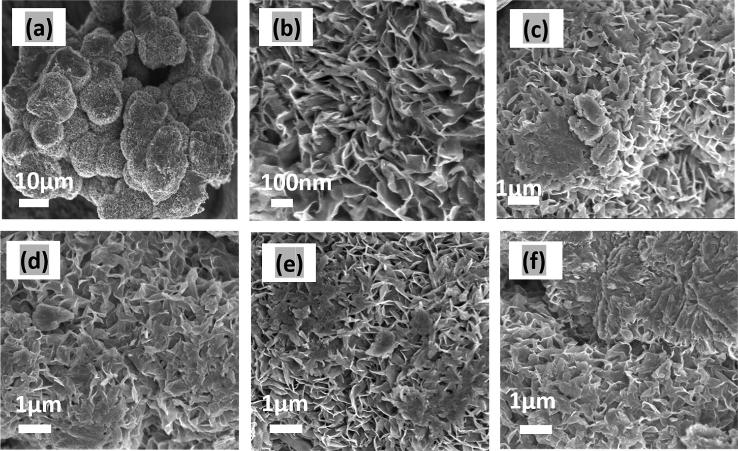 | ||
| Fig. 1 FESEM images of (a) MoS2 under low and (b) MoS2 at high magnification, (c) MoS2/CuO(1 wt%), (d) MoS2/CuO(2 wt%), (e) MoS2/CuO(4 wt%), and (f) MoS2/CuO(6 wt%). | ||
3.2. Structural properties
Fig. 2 illustrates the XRD patterns for MoS2 and MoS2/CuO with different concentrations of CuO. The diffraction peaks for MoS2 were found at 13.96°, 33.96°, 39.47°, and 59.17° corresponding to the reflections from lattice planes (200), (100), (103) and (110), respectively, and they are in good accordance with JCPDS card number 37-1492, confirming the hexagonal structure of 2H-MoS2.35–37 The sharp peaks indicate a good crystalline and well-stacked structure of MoS2.38 For low concentrations of CuO nanoparticles, the diffraction pattern of MoS2/CuO composites was found to be similar to that of MoS2. This suggests that the incorporation of CuO does not change the hexagonal 2H-MoS2 structure. For higher concentrations (6%) of CuO, two additional peaks were observed at 31.9° and 36.8° corresponding to the (110) and (111) planes for CuO, respectively. This further confirms the presence of CuO in the MoS2 nanoflower. Fig. 3 depicts the change in different XRD parameters with the amount of CuO in MoS2. The values of various structural parameters of the synthesized MoS2 and MoS2/CuO are presented in Table 1. The incorporation of CuO caused the (002) peak to shift toward a higher 2θ value compared to that of pure MoS2, suggesting a change in the d-spacing of the composites. The interlayer spacing was calculated using the following equation:| 2dsinθ = nλ |
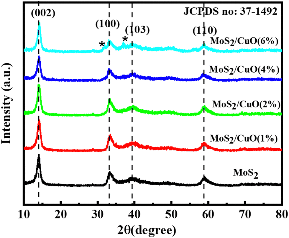 | ||
| Fig. 2 XRD pattern of pristine MoS2 and as prepared MoS2/CuO composites. | ||
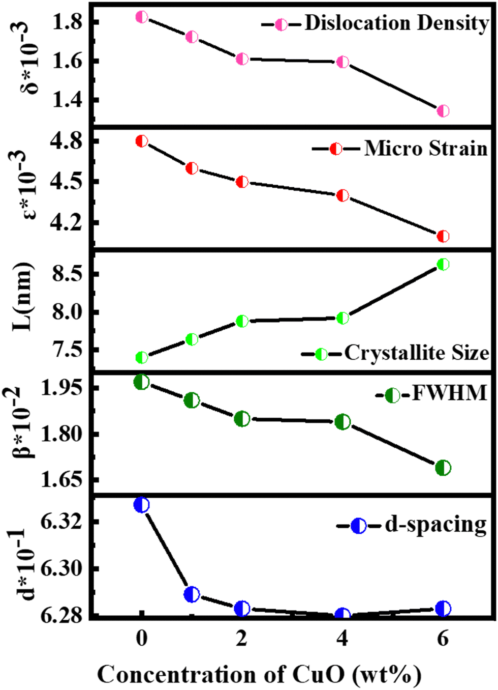 | ||
| Fig. 3 Variation of different XRD parameters as a function of CuO concentration. | ||
| Samples | d-Spacing (nm) | FWHM × 10−2β (radian) | Crystallite size L (nm) | Dislocation density δ × 10−3 | Micro strain ε × 10−3 |
|---|---|---|---|---|---|
| MoS2 | 0.6327 | 1.97 | 7.40 | 18.26 | 4.8 |
| MoS2/CuO(1%) | 0.6289 | 1.91 | 7.64 | 17.23 | 4.6 |
| MoS2/CuO(2%) | 0.6283 | 1.85 | 7.88 | 16.10 | 4.5 |
| MoS2/CuO(4%) | 0.6280 | 1.84 | 7.92 | 15.94 | 4.4 |
| MoS2/CuO(6%) | 0.6283 | 1.69 | 8.63 | 13.43 | 4.1 |
With the increasing amount of CuO, diffraction peaks became narrower, suggesting a reduction in crystallite size. The crystallite size (L) was determined from the (002) plane using the Scherrer formula40
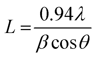
Dislocation density (δ) and microstrain (ε) of the as-prepared samples were measured using the following relationships41
where L, θ, and β denote the crystallite size, diffraction angle, and FWHM of the diffraction peak, respectively.
With the increase in concentration of CuO from 0% to 6%, the value of δ of the nanocomposites was found to be reduced from 18.26 × 10⁻³ to 13.43 × 10⁻³. The microstrain in MoS2 was also found to be reduced from 4.8 × 10⁻³ to 4.1 × 10⁻³ due to the incorporation of CuO nanoparticles. When CuO was incorporated into the MoS2 structure, atoms bound in non-equilibrium positions might have shifted to more equilibrium places, resulting in a reduction in strain.42 And this ordered arrangement of particles in the crystal lattice allows for easier movement of electrons, which is necessary for electrical conductivity.
3.3. Optical properties
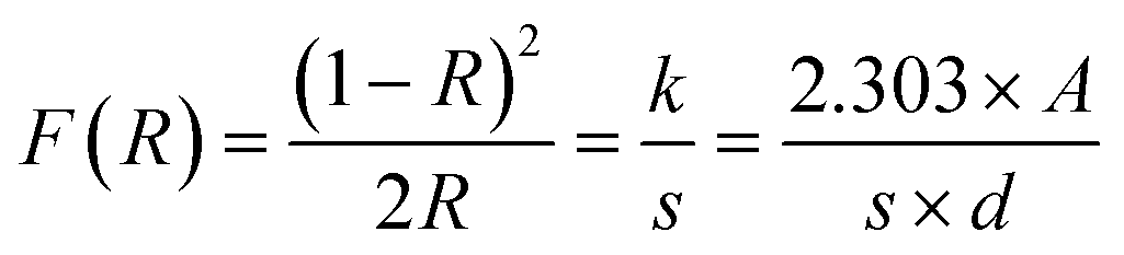
The optical characteristics of all samples have been investigated via analysis of the diffuse reflectance spectra. The absorbance (A) and diffuse reflectance (R) of material are correlated by the Kubelka–Munk (K–M) function, (F(R)), as follows:where absorption and scattering coefficients are represented by k and S, while A and d represent the absorbance and thickness, respectively, of the sample. Fig. 4 shows the K–M function for MoS2 and MoS2/CuO nanocomposites. It was found that with the incorporation of CuO into the MoS2 nanoflowers, the absorbance increased significantly, suggesting a decrease in the optical bandgap in MoS2/CuO composites. Fig. 5 presents the optical band gap of all the samples, which is calculated by plotting corresponding (F(R)hν)1/2vs. photon energy (hν). The estimated band gap of MoS2/CuO composites for different concentrations of CuO nanoparticles is tabulated in Table 2. The optical band gap of MoS2 reduced after the decoration of CuO nanoparticles. The optical bandgap of MoS2 nanoflowers declined from 1.43 eV to 1.08 eV with the increase in CuO concentrations, which align with the previously reported results.43 The incorporation of CuO might introduce additional states near the forbidden energy gap, which can reduce the energy required to excite an electron from the valence band to the conduction band.44
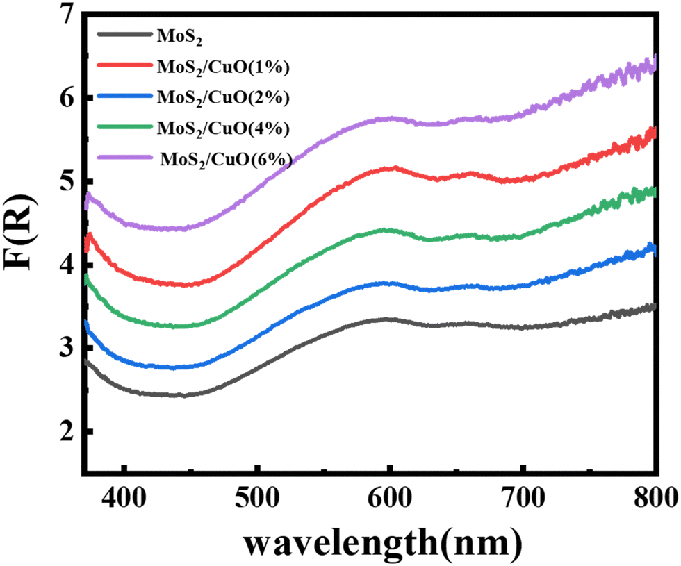 | ||
| Fig. 4 Kubelka–Munk plot, F(R) of MoS2 and its composite with different concentrations of CuO derived from diffuse reflectance spectra. | ||
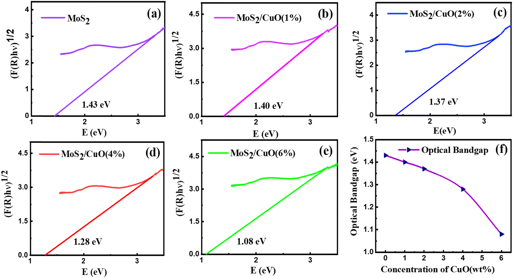 | ||
| Fig. 5 (a)–(e) The Tauc plot of all the as-prepared samples and (f) the variation of the optical bandgap. | ||
| Sample | Optical bandgap (eV) |
|---|---|
| MoS2 | 1.43 |
| MoS2/CuO(1%) | 1.40 |
| MoS2/CuO(2%) | 1.37 |
| MoS2/CuO(4%) | 1.28 |
| MoS2/CuO(6%) | 1.08 |
3.4. Electrochemical properties
Cyclic voltammetry was conducted within a potential window between −0.3 V and 0.2 V at different scan rates (5 mV s−1 to 100 mV s−1). The obtained quasi-rectangular CV curves (Fig. 6(a)–(e)) indicate that the pseudocapacitive mechanism dominates the charge transfer process.45 The area under the CV curve increases with the scanning rate and the current because of the partial intercalation/de-intercalation of electrolyte ions in the electrode. The curves deviated from the ideal rectangular shape, possibly due to the electrolyte ions' temporary movement at the electrode surface.46 The CV curves of different samples at 30 mV s−1 are presented in Fig. 6(f). The incorporation of CuO nanoparticles leads to an increase in the CV area. The electrochemical reaction of MoS2 and CuO in Na2SO4 solution.| MoS2 + Na+ + e− ↔ MoS – SNa |
| CuO + ½H2O + e− ↔ ½Cu2O + OH− |
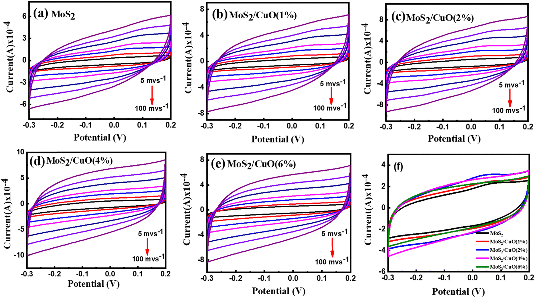 | ||
| Fig. 6 Cyclic voltammetry measurements pristine MoS2 and as prepared composites at different scan rates (a)–(e) and at 30 mV s−1 (f). | ||
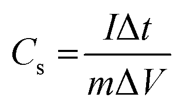
Fig. 7(a)–(e) show the GCD curves of MoS2 and MoS2/CuO at different current densities. In addition, the GCD curve of CuO nanoparticles is shown in the Fig. SF3 (ESI†). The deviation from the symmetric and triangular form is caused by the reversible conversion reaction occurring during the measurement procedure, indicating the pseudocapacitive charge storage mechanism.47Fig. 7(f) illustrates a GCD plot of MoS2 and MoS2/CuO nanocomposites for different concentrations of CuO at a constant current density. The specific capacitance (Cs) can be measured using the following relationship,
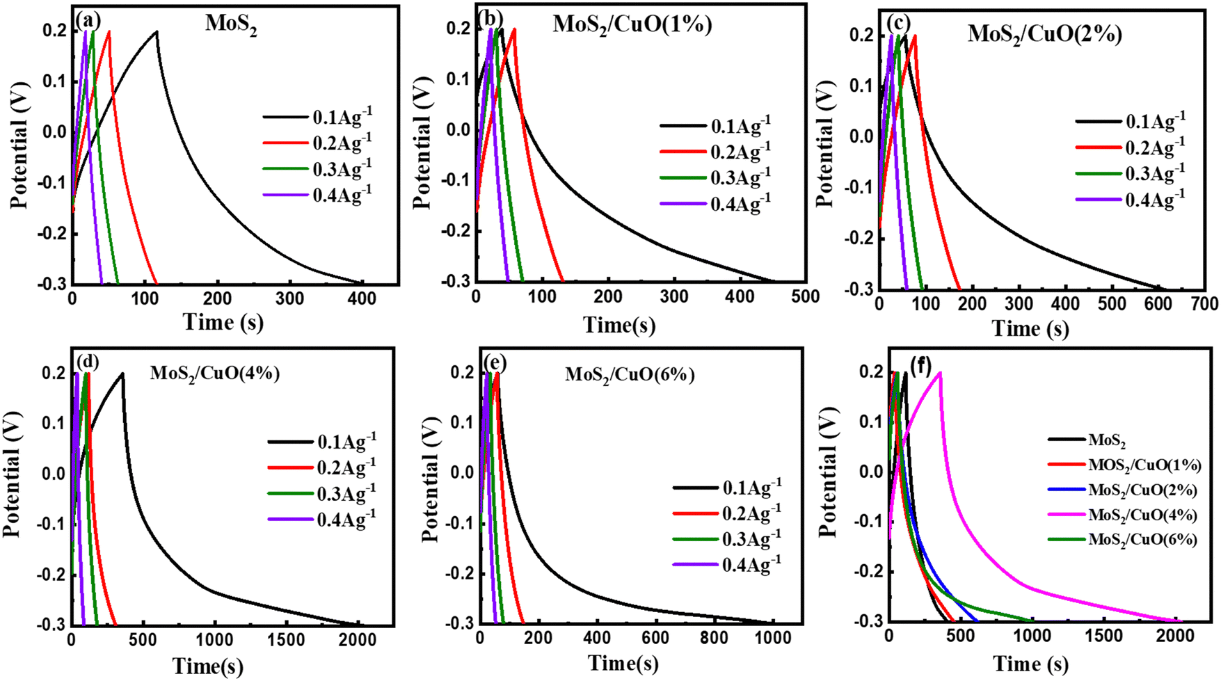 | ||
| Fig. 7 (a)–(e) Galvanostatic charging discharging (GCD) curves of pristine MoS2 and as prepared MoS2/CuO nanocomposites at different current densities and (f) 0.1 A g−1 current density of all samples. | ||
| Sample | Specific capacitance (F g−1) | Energy density W h kg−1 | Power density W kg−1 |
|---|---|---|---|
| MoS2 | 58.07 | 2.02 | 24.94 |
| MoS2/CuO(1%) | 82.93 | 2.88 | 24.96 |
| MoS2/CuO(2%) | 112.44 | 3.90 | 24.97 |
| MoS2/CuO(4%) | 336.23 | 11.67 | 24.99 |
| MoS2/CuO(6%) | 189.14 | 6.57 | 24.98 |
The energy density (E) and power density (P) of MoS2 and MoS2/CuO composites were estimated using the following equations:
The estimated values of E and P for all the samples are presented in Table 3, and the MoS2/CuO(4 wt%) sample gives the highest values.
EIS was implemented to analyze the electrode material's charge-storage mechanism. The Nyquist plot at frequencies between 0.1 HZ to 100 kHz is presented in Fig. 8. This graph displays an inclined line in the lower-frequency region and a semicircular arc in the high-frequency region. A Randles circuit is used to describe the system's faradaic process shown in the inset of Fig. 8, which was constructed to represent the frequency-based electrical performance of the system. The small interception of the semicircle to the x-axis in the high-frequency region, defined by Rs in the circuit, refers to the bulk resistance of the electrolyte. The semicircle represents the response of charge transfer resistance Rct and the impedance of the electrolyte-electrode surface reaction occurring because of the faradaicreaction Rel and EDLC behavior. The Warburg resistance Wo in the circuit symbolizes the impedance caused by the diffusion process and appears in the low-frequency region. The constant phase elements (CPE) in the circuit are capacitive elements. Table 4 presents the EIS fitting parameters of MoS2 and MoS2/CuO composites obtained from simulation. The series resistance was found to be similar for all the samples. An observable change in the charge transfer resistance was found. The value of Rct was significantly reduced as the amount of CuO rose, suggesting that the addition of CuO boosted conductivity. The lowest value of Rct was obtained for the MoS2/CuO(4 wt%) composite, suggesting that MoS2/CuO(4 wt%) possesses the best ion conducting ability among all samples. This result is also consistent with CV and GCD results.49
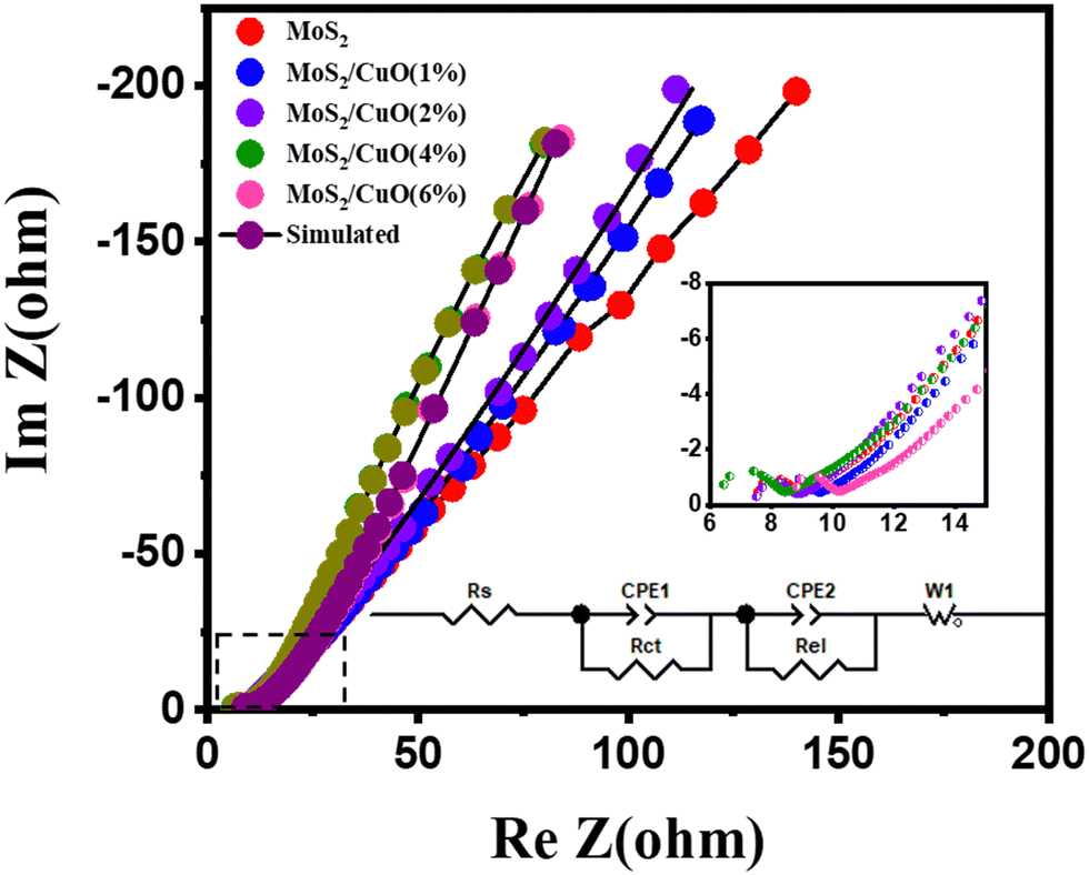 | ||
| Fig. 8 Modeled and observed Nyquist plots of different samples. The line shows the fitted Nyquist plot for different samples. The inset in the figure shows the magnified image at high frequency and the equivalent circuit used for the simulation. | ||
| Sample | R s (Ohm) | R el (Ohm) | R ct (Ohm) |
|---|---|---|---|
| MoS2 | 7.40 | 0.76 | 26.64 |
| MoS2/CuO(1 wt%) | 7.78 | 1.43 | 56.90 |
| MoS2/CuO(2 wt%) | 7.57 | 1.01 | 51.63 |
| MoS2/CuO(4 wt%) | 6.28 | 1.21 | 10.60 |
| MoS2/CuO(6 wt%) | 8.47 | 1.23 | 20.93 |
The cyclic stability of MoS2/CuO(4 wt%) was investigated for 6000 charging/discharging cycles at a constant current density, shown in Fig. 9(a). A capacitance retention of ∼84% was achieved after completing 6000 cycles of operation. A Coulombic efficiency of 113% was achieved in the first cycle, which was found to be 108% in the last cycle. The close interaction of the CuO nanoparticles with MoS2 improves the cyclic stability of the heterostructure. Fig. 9(b) presents the Nyquist plot of MoS2/CuO(4 wt%) taken before the 1st cycle and after the 6000th cycle of the charging–discharging test. The size of the semicircle in the high-frequency region became larger after 6000 cycles of charging and discharging than that after the 1st cycle. The series resistance dropped after the cycles, whereas the charge transfer resistance Rct and Rel increased, revealing a lessening in the conductivity of MoS2/CuO(4 wt%). Because of the repetitive expansion and contraction during charging and discharging, the crystal structure of the active material might have altered or got damaged, causing a decrease in conductivity.50,51Table 5 presents the fitting parameters before and after the charge–discharge cycles.
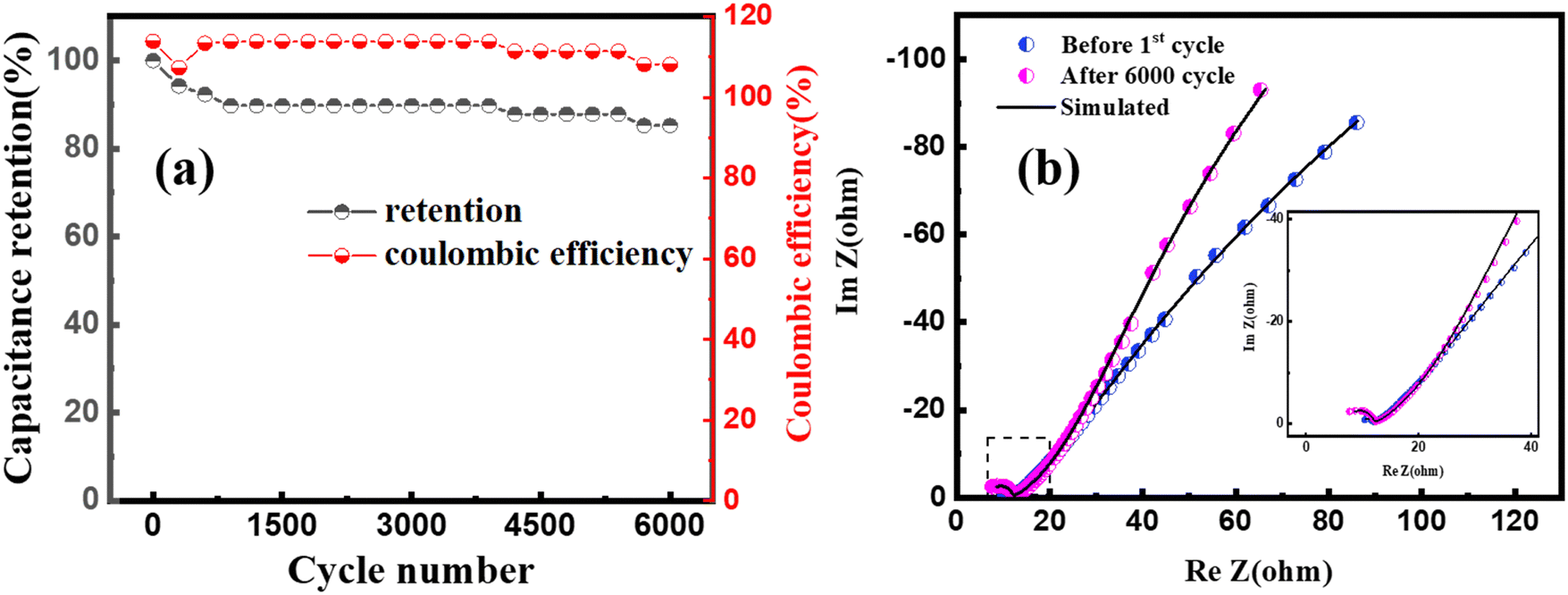 | ||
| Fig. 9 (a) Cyclic stability performance of MoS2/CuO(4 wt%) at a current density of 5 A g−1 (b) Nyquist plot for the MoS2/CuO(4 wt%) sample before the 1st cycle and after 6000 cycles. | ||
| Cycle | R s (Ohm) | R el (Ohm) | R ct (Ohm) |
|---|---|---|---|
| 1 | 9.93 | 1.1 | 10.1 |
| 6000 | 6.80 | 4.5 | 20.8 |
3.5. MoS2/CuO(4 wt%) electrode material
The incorporation of CuO nanoparticles improved the electrochemical performance, and a CS of 336.23 F g−1 along with an energy density of 11.67 W h kg−1 has been achieved for the MoS2/CuO(4 wt%) nanocomposite. The layered structure of MoS2/CuO composites contains abundant channels for electrolyte transportation. The increased concentration of CuO provided a larger surface area for the electrochemical reaction. A large crystallite size caused more intercalation of ions, increasing electronic conductivity up to the amount of 4 wt% of CuO in MoS2, but a further increase in CuO concentration (e.g., 6 wt%) diminished the electrochemical properties, attributed to the smaller surface area caused by the increase in d-spacing.The material exhibited remarkable cyclic stability and demonstrated outstanding retention of capacitance. The study's notable findings illustrate the potential of the MoS2/CuO nanocomposite as a viable electrode material for energy storage purposes. Table 6 displays the specific capacitance values of nanocomposite materials based on MoS2 with varying morphologies. Table 6 displays that the MoS2/CuO(4 wt%) nanocomposite shows a higher specific capacitance than previously reported values. The remarkable outcome was attained due to the nanocomposite's improved interlayer spacing, active sites, and defect states.
| Composite | Morphology | Specific capacitance (F g−1) | Ref. |
|---|---|---|---|
| MoS2/C | Nanoflower | 201.4 F g−1 (0.2 A g−1) | 52 |
| MoS2/graphene-foam | Nanosheet | 48.85 F g−1 (1 A g−1) | 53 |
| MoS2/Ti-plate | Nanosheet | 133 F g−1 (1 A g−1) | 54 |
| Ni3S4/MoS2 | Nanosheet | 108 F g−1 (0.5 A g−1) | 55 |
| SnS2/MoS2 | Nanoflower | 105.7 F g−1 (2.35 A g−1) | 56 |
| MoS2/ZnO | Nanoflower | 42 F g−1 (1 A g−1) | 57 |
| MoS2/CuO | Nanoflower | 336.23 F g−1 (0.1 A g−1) | This work |
3.6. Computational models
According to the experimental findings, semiconducting 2H-MoS2 has been observed and the {002} planes are the favored orientation of hexagonal 2H-MoS2 nanoflowers.58,59 The computational study is performed with the creation of MoS2 nano-flowers (nF-MoS2) by utilizing of a 2 × 2 supercell that consists of bilayer MoS2 oriented along the [002] direction, as illustrated in Fig. 10c. The interatomic distance between Mo and S atoms is measured to be 2.411 Å. Upon relaxation of the vacuum slab consisting of two layers of MoS2, a slight increase in this bond length is observed. The interlayer spacing was 7.4395 Å and 6.181 Å for the bulk and vacuum surface slab, respectively. The relaxed lattice parameter values of hexagonal MoS2 are reported as a = b = 6.3806 Å and c = 14.879 Å for the bulk configuration (as shown in Fig. 10a), and a = b = 6.3687 Å and c = 30.3082 Å for the vacuum slab configuration with a vacuum of 20 Å (as shown in Fig. 10e).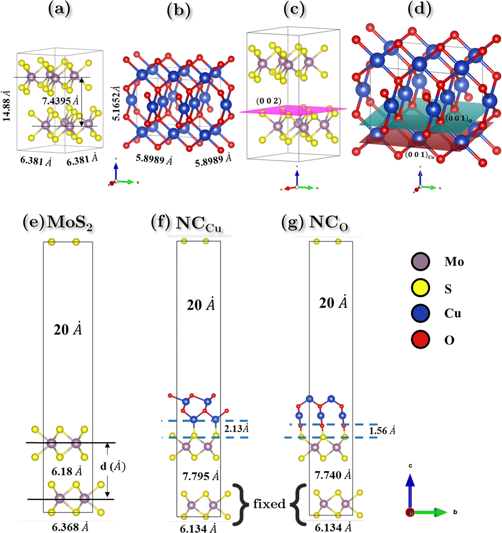 | ||
| Fig. 10 Base supercell structures along with their lattice parameters for (a) bilayer MoS2 and (b) CuO. Lattice planes showing predominant surface plane(s) for (c) nF-MoS2 (002) and (d) nP-CuO(001) with Cu and O terminations. (e) Surface slab of MoS2 and (f) and (g) interface model for the nF-MoS2/nP-CuO nanocomposite with Cu (NCCu) and O (NCO) terminations, respectively, with 20 Å of vacuum along the c direction. | ||
CuO exhibits different oxidation states, crystal structures, and electronic behavior. These differences in the crystal structure and electronic behavior are due to strong electron correlation in CuO.60 The morphology of CuO nanoparticles depends on the precursor materials and synthesis pathways employed, resulting in a diverse array of geometric configurations. Different surface orientations are observed for various shapes. CuO nanoparticles have a monoclinic crystal structure, and the {111} planes are the most stable surface planes.61 However, when a heterogeneous nanostructure is formed between nF-MoS2 and nP-CuO, CuO slices are inserted into MoS2 petals, and these CuO slices have a layered structure with {001} planes.62,63 And on these planes, surface termination is possible for both Cu and O.64 An appropriate CuO supercell was constructed to model this specific termination behavior. Upon conducting geometric optimization of the CuO bulk supercell, the relaxed structure depicted in Fig. 10(b) exhibits lattice parameters of a = b ≈ 5.9 Å and c = 5.17 Å.
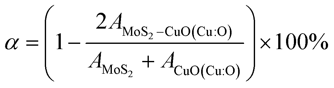
In our study of the nanocomposite interface, we utilized a single layer of the relaxed CuO structure featuring termination by both copper (Cu) and oxygen (O). In both heterostructures, the lattice parameters exhibited identical values for both the a and b directions while maintaining a 20 Å vacuum in the c direction to prevent any potential self-interaction errors. The numerical values of the lattice parameters a and b are determined to be 6.1338 Å, while the parameter c is measured to be 37.3742 Å. The angle between a and b is found to be 105.038°, as depicted in Fig. 10f and g. Additionally, the lattice mismatch parameter α is estimated to be approximately 0.35%, which is computed using the following equation:
3.7. Electronic properties
Fig. 11 shows the atomic band projected band structure of MoS2 with an indirect bandgap (a) with and (b) without accounting for van der Waals interactions, the atomic band projection, and the band projected onto the MoS2 surface slab for (c) and (d) NCCu, (e), (f) NCO nanocomposite interfaces. Here, VBM = EF = 0.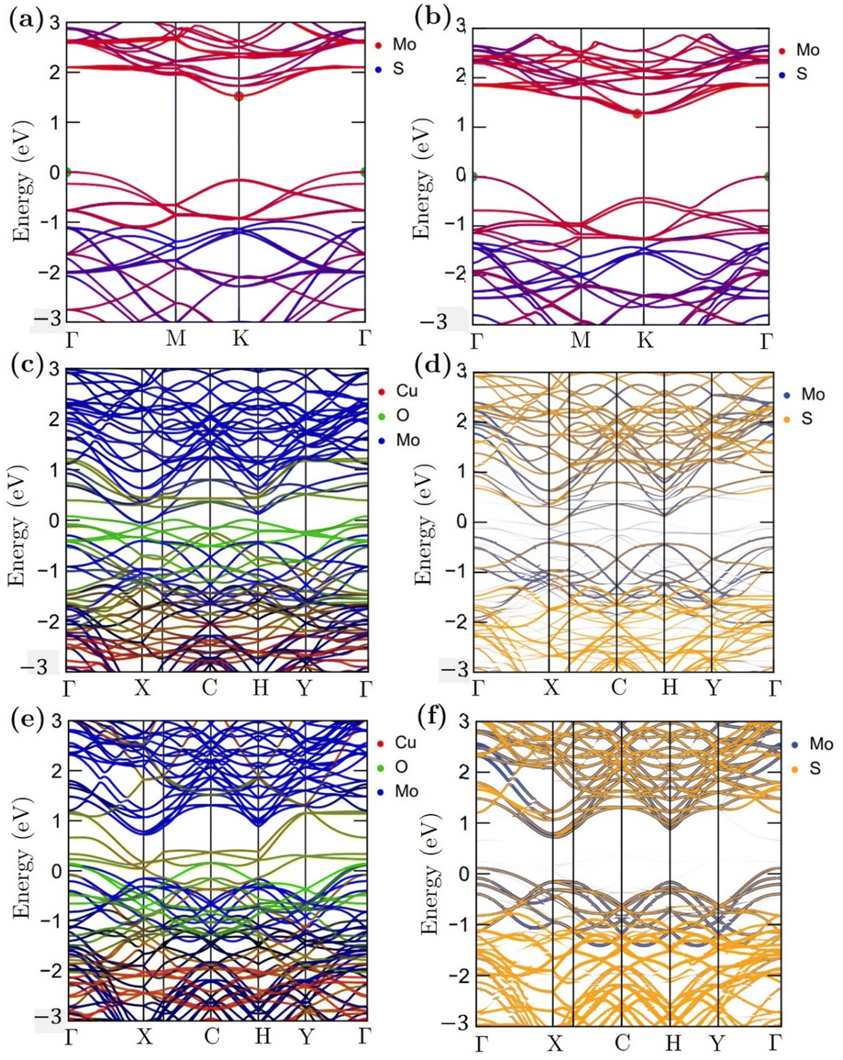 | ||
| Fig. 11 Atomic band projected band structure of the MoS2 surface slab with an indirect bandgap (a) with and (b) without accounting for van der Waals interactions, atomic band projection and the band projected onto the MoS2 surface slab for (c) and (d) NCCu and (e) and (f) NCO nanocomposite interfaces. Here, VBM = EF = 0. | ||
The analysis of atomic bands reveals that the MoS2 bilayer has an indirect band gap of 1.52 and 1.17 eV, with and without dispersion correction, respectively (as depicted in Fig. 11(a) and (b)). These values are smaller than the experimental value (1.6 eV).58 Also the valence band maximum (VBM) and conduction band minimum (CBM) are found to be predominantly composed of Mo atoms, with a minor contribution from S atoms in the case of VBM. The analysis of the projected density of states (PDOS) calculation reveals that the VBM and CBM are derived from the 4d and 4p orbitals of the Mo atoms, respectively. The interfacial states near the Fermi level in the NCCu and NCO systems are primarily composed of O-2p states, as evidenced by the TDOS and band structure illustrated in Fig. 11c, e and 12a. Notably, the interfacial states in the NCCu system are dominated by O-2p orbitals. In contrast, these orbitals have minimal influence in the NCO system, as demonstrated by the projected density of states (PDOS) analysis of Mo-4d, Cu-3d, and O-2p orbitals in Fig. 12c and d. Moreover, the interfacial interactions have modified the Mo-d orbitals more for NCCu than NCO, shifting the orbitals to the left towards lower energy in both cases. In our experimental study, the primary component is nF-MoS2, while nP-CuO is added in a minor capacity, serving solely as a modifier. MoS2 predominantly governs the electronic characteristics, and the MoS2–CuO interface is a critical factor in altering this basic electronic configuration. As the CuO content increases, the impact of interfacial interaction becomes more pronounced. Our findings reveal a significant impact on the band structure (as depicted in Fig. 11d and f), with the most prominent feature being a reduction in the band gap. This observation is further supported by experimental evidence. Due to a comparative abundance of O-2p states near the band gap of NCCu with respect to NCO, the projected band gap of NCCu is smaller than that of NCO, around 0.2 eV compared to 0.9 eV. Although the calculated band gaps of MoS2 and CuO (001: Cu, O) in this work were underestimated using the GGA+U functional, the relative trends between these values were still helpful in analyzing the charge-carrier transfer behavior. The hybridization between the 3p states of the modified d orbitals from Mo sites and p orbitals from O sites in the interface region helps to maintain an increased number of states near the Fermi level by reinforcing their presence, and as a result, we get two positive outcomes. One is that the projected band gap of MoS2 has decreased, resulting in a higher conductivity suitable for capacitance. Another outcome is that the increased states result in a higher density of available states for charge storage, as shown in the quantum capacitance calculation, resulting in an increased specific capacitance for CuO-incorporated MoS2. The Cu-3d states are not present near the Fermi level as they reside deep inside the VBs. Another important observation from Fig. 12e is that the TDOSs have shifted towards lower energy, which is more prominent for NCO due to a stronger interfacial dipole than NCCu.
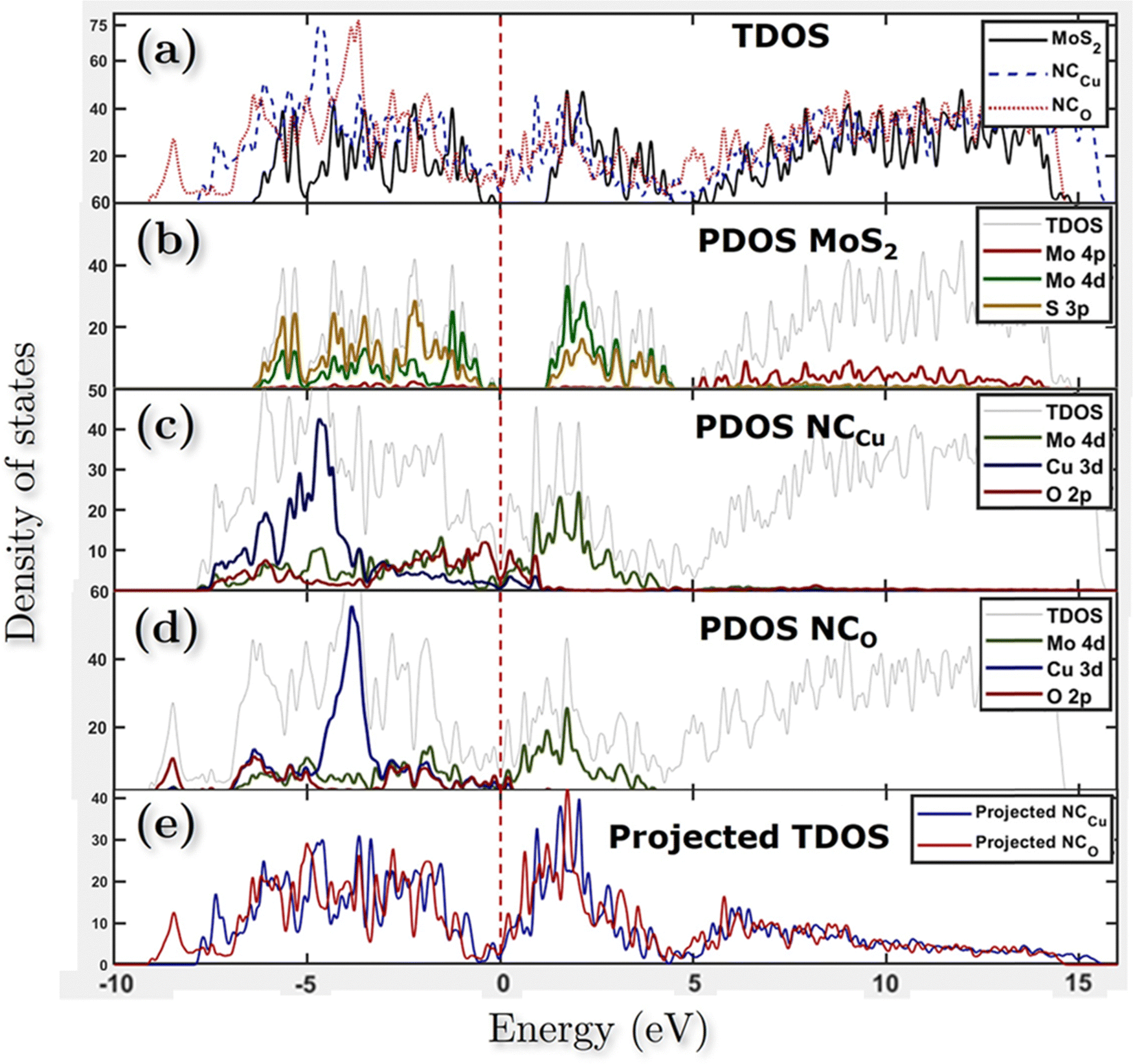 | ||
| Fig. 12 (a) Total density of states (TDOS) for all models and projected density of states (PDOS) of (b) MoS2 surface slab, (c) NCCu, (d) NCO and (e) TDOS for both NCCu and NCO models only projected onto the MoS2 slab. Here, VBM = EF = 0. | ||
3.8. Simulated optical properties
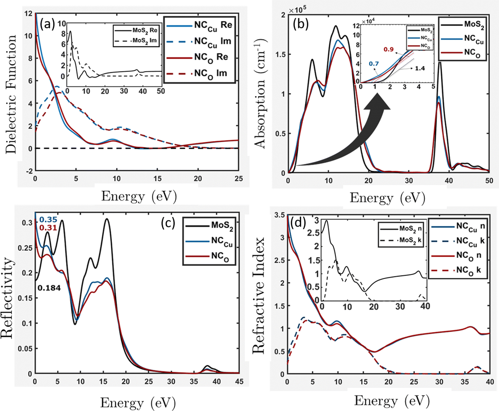
This study investigates the electronic transitions responsible for the optical properties observed in the surface slab of MoS2 and in NCCu and NCO. Fig. 13a (inset) illustrates that for a MoS2 surface slab, the lowest energy incident photons result in the most positive value for the real part, while the imaginary part approaches zero. In contrast, the heterostructures exhibit an exponential increase in their actual value, resulting in a significantly high positive value for low-energy photons. Additionally, the imaginary component is non-zero and comparatively greater for NCCu than for NCO. The absorption coefficient measures the proportion of energy that a wave loses as it traverses a substance, resulting in a decrease in intensity at a distance x from the surface, as expressed by the equation:| I(x) = I(0)exp(−ηx) |
 with k denoting the imaginary component of refractive index and ω representing the frequency of light. As depicted in Fig. 13b, the absorption coefficient has exhibited a reduction across the entire spectrum of photon energy for both heterostructures, resulting in a red shift towards lower energy levels compared with the MoS2 slab. As a result of the red shift, a greater quantity of low-energy photons will be absorbed compared to the MoS2 surface slab. As the CuO content rises, it has been noted that the optical band gap is reduced. Consequently, the nanocomposite exhibits a greater capacity for absorbing photons with lower energy levels. The optical band gaps (Fig. 13b inset) are around 1.4 eV, 0.7 eV, and 0.9 eV for MoS2, NCCu, and NCO, respectively. The MoS2/CuO nanocomposite exhibits a smaller bandgap than the pure MoS2 nanoparticles, and the presence of intermediate states may contribute to an increase in the nanocomposite's conductivity. This enhanced conductivity may subsequently lead to a rise in the nanocomposite's capacitance.
 | ||
| Fig. 13 Optical properties (a) dielectric function, (b) absorption, (c) reflectivity and (d) refractive index for the MoS2 surface slab, NCCu and NCO. | ||
The NCCu exhibits a reflectivity of approximately 35%, while the NCO demonstrates a reflectivity of about 31%. These values are comparatively higher than the reflectivity of the MoS2 surface slab, about 18%, as depicted in Fig. 13c.
Typically, the difference in transmitting an electromagnetic wave across a vacuum and other substances can be explicated by a complex refractive index. For transparent materials, this index is exclusively real. In the case of MoS2 surface slabs and heterostructures, it can be observed that both the real and imaginary components make a significant contribution across most of the energy spectrum. In the vicinity of low photon energy, it can be observed that the refractive index of the MoS2 surface slab is entirely real, approximately 2.5, as depicted in the inset of Fig. 13d. In both heterostructures depicted in Fig. 13d, the lower energy range exhibits comparable characteristics to its dielectric function. Specifically, the real component of the refractive index increases exponentially, while the imaginary component remains non-zero.
3.9. Interfacial structure
Upon relaxation, the distance between the nF-MoS2 and nP-CuO interface was determined to be 2.13 Å for NCCu. Additionally, the interlayer spacing between MoS2 layers increased from 6.18 Å to 7.795 Å. The interfacial distance between the two heterostructures in NCO has been observed to decrease to 1.56 Å, while the interlayer distance of MoS2 reduces from 7.795 Å to 7.74 Å.The calculation of the surface energy of the MoS2 surface oriented along the (002) direction is performed through the utilization of equation in the following manner,
| Esurf = EMoS2–bulk − EMoS2–surface slab |
To assess the interfacial stability of the composites quantitatively, the interfacial interaction energy (Eint) was calculated using the formula
| Eint = EMoS2–CuO(Cu:O) − EMoS2 − ECuO |
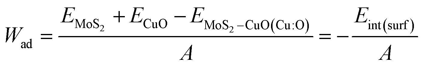
The variable Eint(surf) represents the interfacial (surface) interaction energy, expressed as a negative value, and A denotes the interfacial area.
Table 7 indicates that the surface and interfacial energies exhibit negative values, signifying stability. Notably, NCCu demonstrates the most stable configuration, with an interfacial interaction energy of −4.8 eV, the lowest among the observed values. In terms of both interfacial distances and energetics, NCCu aligns more closely with experimental findings. The experimentally observed interfacial distance is around 2.54 Å, similar to our calculated value of 2.13 Å, and the inter-layer distance between MoS2 layers has increased in both cases.62 Moreover, according to previous research, adsorption distances between 2.0 Å and 2.5 Å indicate chemical interactions.65 Based on this criterion, all the studied systems exhibit chemisorption behavior. This strong interaction between MoS2 and CuO can prevent other MoS2 layers from sticking to themselves, resulting in a more exposed active surface area.
To gain insight into the bond properties of the suggested models, a Mulliken bond population computation was carried out. Sanchez-Portal et al. have proposed a method for population analysis, which involves projecting the plane wave (PW) states onto a localized basis.67 Subsequently, the studied states are analyzed using a Mulliken formalism-based population approach.68 The utilization of the overlap population can help in determining whether a bond is covalent or ionic. A high population is indicative of a covalent bond, while a low bond population value is indicative of an ionic contact. The findings presented in Table 7 suggest a decreasing trend in the covalence of the Mo–S bond for the MoS2 layer in proximity to the interface exhibits, with the MoS2 surface slab demonstrating the highest covalence, followed by NCCu and NCO. Regarding NCCu and NCO heterostructures, the Cu–O bond exhibits a higher degree of ionic character than the Cu–S bond. Additionally, a comparison between the two heterostructures reveals that the Cu–O bond in NCCu displays a greater level of covalency than that in NCO.
3.10. Redistribution of charge
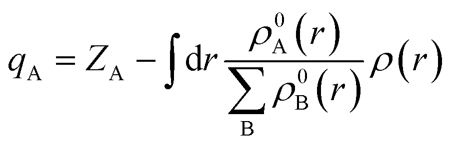
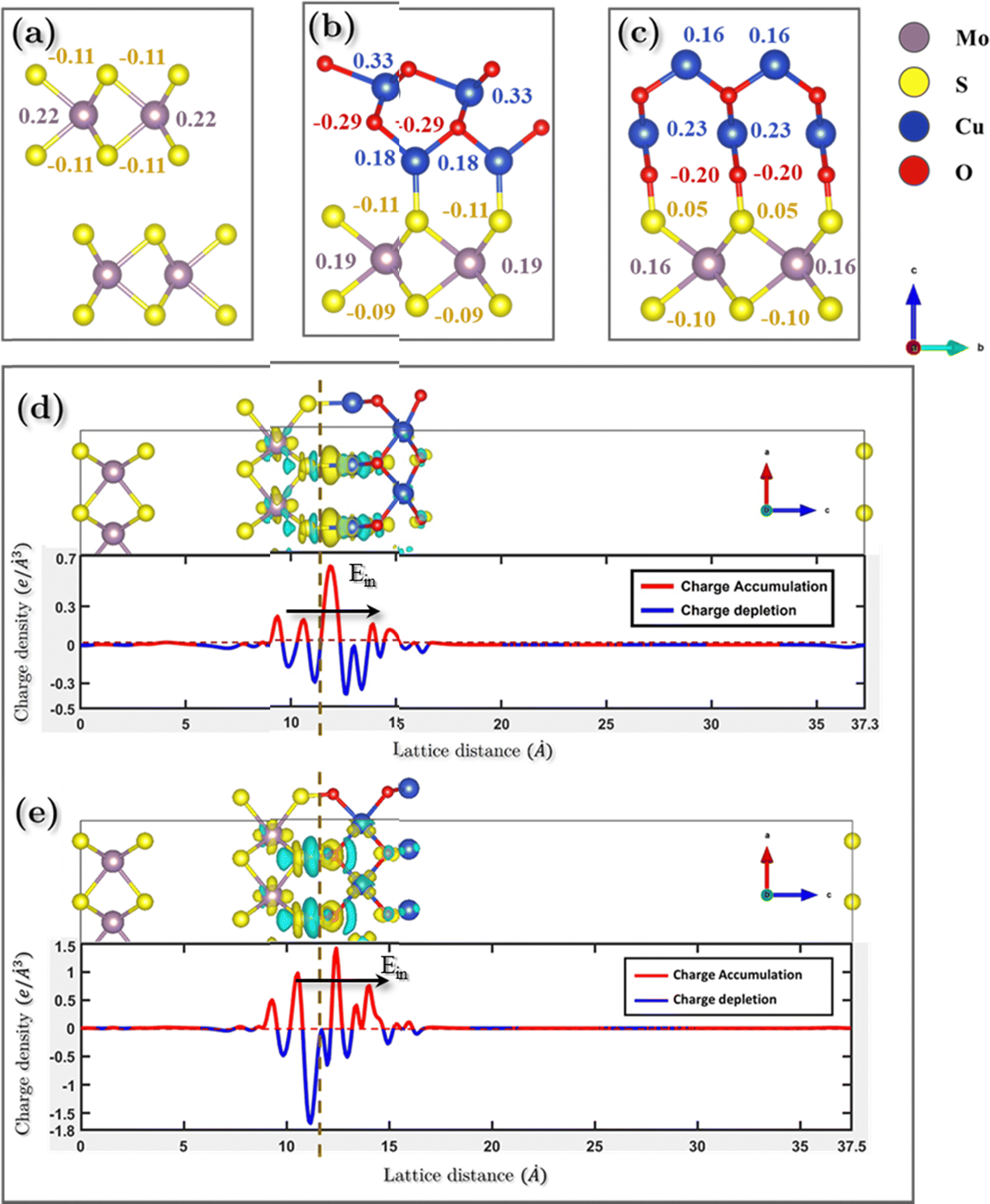
To offer quantitative depictions of the charge distributions, it is advantageous to partition the system into distinct atomic fragments. As defined by Hirshfeld charge,69 the deformation density is the distinguishing factor between molecular and unrelaxed atomic charge densities. A general approach is to distribute the charge density among the atoms at every location in a manner that corresponds to their respective free-atom densities at the corresponding distances from the nucleus. The aforementioned prescription results in bonded-atom distributions that are highly localized and exhibit a close resemblance to the molecular density in their respective vicinity. The definition of the charge on atom A, qA, is given using the following equation:The equation mentioned above pertains to the nuclear charge of element A, denoted as ZA, the isolated ground-state atomic density of element B, represented as ρ0B, and the molecular density, characterized as ρ. The Hirshfeld charges are prone to underestimation when compared to empirical data. As per the Hirshfeld charge analysis, it can be observed that the atom-centered negative charge on the sulfur atoms of the MoS2 layer for both heterostructures (Fig. 14b and c) has decreased compared to the MoS2 surface slab (Fig. 14a).
 | ||
| Fig. 14 Atomic charge distributions using Hirshfeld charge analysis for (a) MoS2 surface slab, (b) NCCu and (c) NCO. Charge density differences (3D plot, yellow = charge accumulation and blue = charge depletion) and average charge density differences (line plot) of (d) NCCu and (e) NCO. | ||
This decrease in the negative charge on the S atoms means they are less polarizable. As we know, van der Waals force is proportional to the polarizability of the molecules, and so more polarizable molecules will experience a stronger van der Waals force. The observed expansion of interlayer spacing in the MoS2 bilayer can be attributed to a reduction in the van der Waals attractive force. The disparity in charge between interfacial O–S atoms in NCO is more pronounced than that between Cu–S atoms in NCCu. This leads to the inference that the charges in NCCu are centered on the bond, whereas NCO charges are centered on the atom. This distinction will be further elucidated in the subsequent analysis of the charge density difference.
To gain a deeper understanding of the electronic structure evolution resulting from interfacial interaction, the charge density differences were computed (as depicted in Fig. 14). The definition of the charge density difference was established as presented in eqn (1),
| Δρdifference = ρtotal − Σρi | (1) |
The phenomenon of charge separation is observed to be more pronounced in the NCO model as compared to NCCu. This is attributed to the formation of strong S–O chemical bonds at the interface of the NCO model, which serves as a significant driving force for facilitating the transfer of charges. The observed phenomenon entailed a reduction in electron density oscillation from the MoS2–CuO interface. Regarding NCCu, the redistribution of charges is confined to the interfacial vacuum region, in contrast to the previous scenario where the charge redistribution was primarily concentrated on the Cu–S bond. Moreover, the charge redistribution is concentrated mainly in the interfacial region between the first layer of the MoS2, which is consistent with the fact that gap states are mainly present in the first layer of MoS2. In other words, gap states do not significantly penetrate into the “bulk” region of MoS2. Upon closer examination, it is observed that the electrons on the CuO side extend about 0.87 Å and 2.2 Å for NCCu and NCO, respectively, while the positive charges on the MoS2 side extend about 3 Å for NCCu and 3.22 Å for NCO, respectively. Overall, the electrons extend over a shorter distance in the CuO region compared to MoS2. This can be attributed to the high electron density of CuO.
The transfer of net charge from the MoS2 slab to the CuO monolayer yields a significant inherent built-in electric field (Ein) that extends from MoS2 to CuO. The significant electric field that is inherently present facilitates the movement of electrons from CuO toward MoS2, thereby enhancing the interlayer coupling. The phenomenon of charge density attraction between MoS2 and CuO is believed to play a significant role in augmenting the charge storage capacity of the composite.
3.11. Quantum capacitance
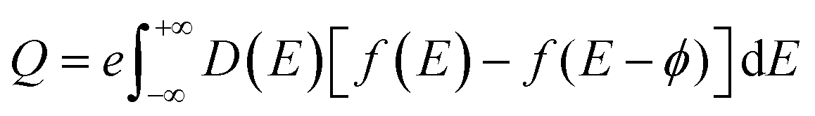
To elucidate the increased specific capacitance due to the incorporation of CuO, we performed calculations to determine the quantum capacitance (CQ) of pure MoS2 and CuO incorporated nanocomposites utilizing the DOS of MoS2 and MoS2/CuO nanocomposites. The concept of quantum capacitance refers to the manner in which excessive charges, specifically ions, respond to a change in applied potential and is measured as the rate of this change.70 The expression for the derivative of the net charge on the substrate or electrode with respect to electrostatic potential can be formulated as follows,where Q is the electrode's excessive charge and ϕ is the chemical potential. The overall electric charge is directly proportional to the weighted summation of the electronic states' density up to the Fermi energy level EF. This charge can be expressed as an integral involving the electronic density of state D(E) and the Fermi–Dirac distribution function f(E) as follows:
Hence, it is possible to compute the quantum capacitance (CQ) of a channel at a non-zero temperature T by utilizing the density of states (DOS) as,
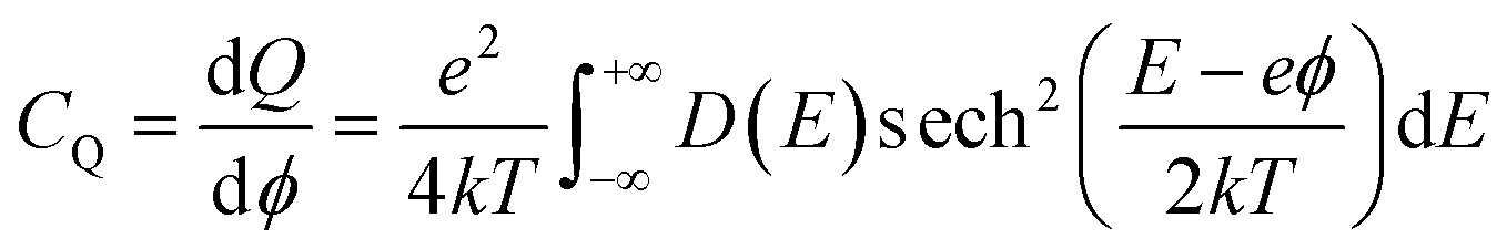 | (2) |
The aforementioned equation involves the charge of electrons denoted by e, the chemical potential represented by ϕ, the density of states (DOS) indicated by D(E), and the Boltzmann constant represented by k. Thus, the computation of the charge quantization for the entire system has been approximated solely based on the density of states. The study employed a potential window ranging from −0.5 to 0.5 V, which was determined based on the established limit of MoS2 capacitance in aqueous electrolytes, as reported in the literature.71
From Fig. 15, it can be observed that NCCu and NCO show CQ values of around 401.3 and 302.1 F g−1 near the Fermi level (EF = 0), representing an increase of around 6.6-fold and 5-fold, respectively, compared to pure MoS2, which has a CQ value of around 61.01 F g−1. These values are comparable to our experimental calculation of specific capacitance shown in Table 3. The highest specific capacitance was found for 4 wt% CuO incorporation with a value of 336.23 F g−1, which is 5.8-fold greater than that of pure MoS2, which shows a specific capacitance value of 58.07 F g−1. This trend is consistent with theoretical calculations.
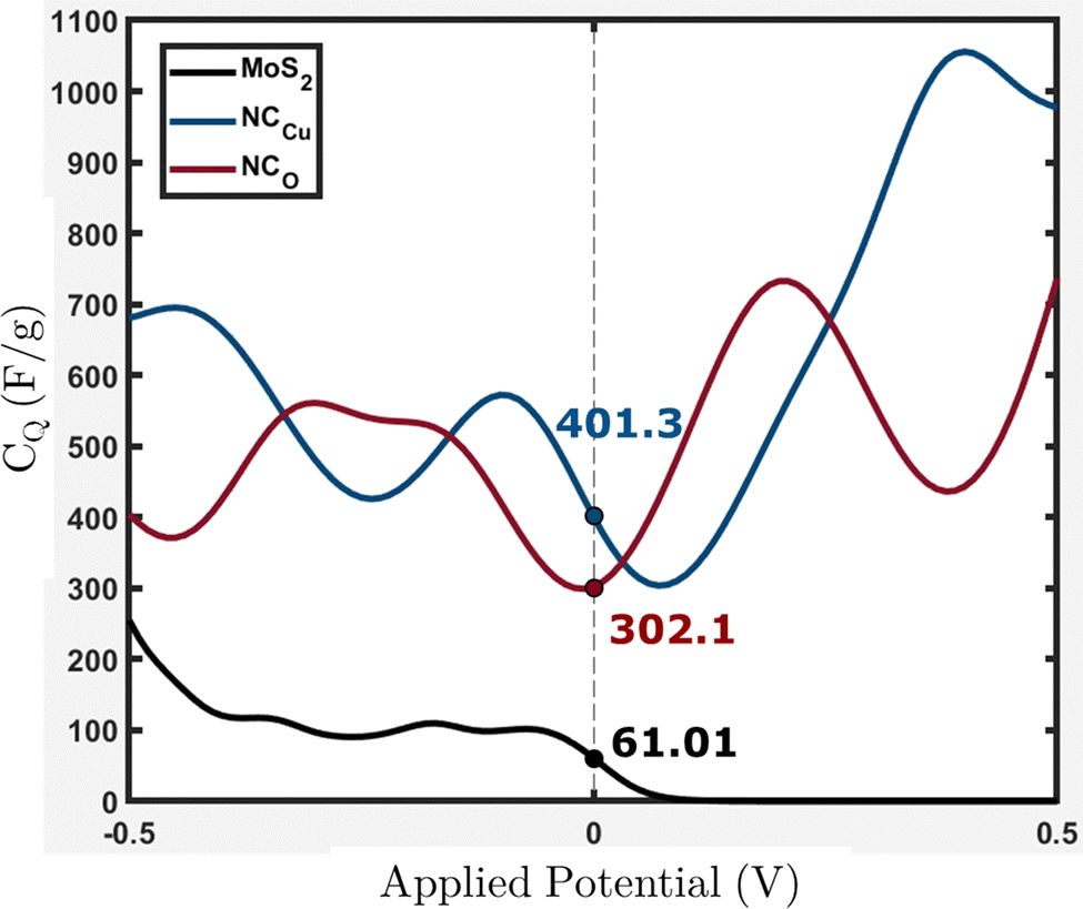 | ||
| Fig. 15 Calculated quantum capacitance (CQ) for the MoS2 surface slab, NCCu and NCO with values near EF = 0. | ||
Eqn (2) presents the formulation of CQ, indicating that the quantum capacitance exhibits a direct correlation with the density of states in the vicinity of the Fermi energy. The contribution of states that are energetically distant from the Fermi level is negligible. This is because the energy relative to the Fermi level is represented by (E − eϕ), and the function sech2(x) approaches zero rapidly for |x| > 0. The increased capacitance observed in CuO-incorporated MoS2 nanocomposites can be attributed to the amplified density of states near the Fermi level. The origin of these states has been discussed in the electronic properties section.
In summary, the hybrid experimental and computational study has demonstrated that the inclusion of CuO has resulted in an augmentation of the charge storage capacity and specific capacitance of MoS2 for various reasons. (1) CuO slices possessing a layered structure with {001} planes have the potential to demonstrate super capacitance behavior independently. (2) MoS2 nanosheets can function as a substrate to uniformly hold CuO nanoparticles, thereby preventing their agglomeration. (3) Likewise, introducing CuO slices can prevent the restacking of MoS2 nanosheets. (4) Using modified MoS2 nanosheets results in a considerably greater active surface area. (5) The inclusion of CuO would lead to the generation of numerous energy levels in proximity to the Fermi level. The collective impact of these factors can enhance the specific capacitance of MoS2 nanoflowers synergistically.
4. Conclusion
In brief, a hydrothermal synthesis method was employed to fabricate MoS2/CuO composite nanomaterials with varying concentrations of CuO nanoparticles. The electrochemical investigation revealed that the inclusion of CuO nanoparticles resulted in a noteworthy enhancement of the electrochemical efficacy of MoS2/CuO nanocomposites. The study showed that the MoS2/CuO(4%) composite material demonstrated a specific capacitance of 336.23 F g−1 and an energy density of 24.99 W h kg−1 when subjected to a current density of 0.1 A g−1. Furthermore, the specimen demonstrates exceptional cyclic stability, evidenced by its capacitive retention rate of 89.7% even after 4000 cycles. From a structural, morphological standpoint, the theoretical calculations suggest that the incorporation of CuO nanoparticles can prevent the restacking of MoS2 layers due to their assertive chemisorption behavior, thus increasing the active surface area for the intercalation of charges and ions. The hybridization in the interface region between Mo and O orbitals leads to an increase in states near the Fermi level, resulting in higher conductivity and specific capacitance for MoS2 with CuO incorporation. Due to these states, we see a decreasing trend in the optical band gap from absorbance calculations, resulting in higher conductivity. Moreover, the quantum capacitance calculations demonstrate that these newly generated states can accommodate more charge. The charge transfer from MoS2 to CuO results in a strong intrinsic electric field that improves electron transfer and creates a longer path for the charges. As a result, the charging and discharging processes take longer, resulting in increased specific capacitance of MoS2. Thus, the presented experimental and theoretical evidence indicates that the inclusion of CuO into MoS2 yields a beneficial synergistic outcome, leading to a promising material that can effectively compete in advanced energy storage applications.Conflicts of interest
There are no conflicts to declare.Acknowledgements
One of the authors, MRI, gratefully acknowledges the financial support from the Ministry of Science and Technology, Government of Bangladesh, under the grant: 39.00.0000.009.99.024.22-901 (Project ID# SRG-226633). IMS and NF are also grateful to the Semiconductor Technology Research Center (STRC) of the Department of Physics, University of Dhaka, for providing technical support.References
- J. Zhan, G. Li, Q. Gu, H. Wu, L. Su and L. Wang, Porous Carbon Nanosheets Armoring 3D Current Collectors toward Ultrahigh Mass Loading for High-Energy-Density All-Solid-State Supercapacitors, ACS Appl. Mater. Interfaces, 2021, 13(44), 52519–52529 CrossRef CAS PubMed.
- J. R. Miller and P. Simon, Electrochemical capacitors for energy management, Science, 2008, 321(5889), 651–652 CrossRef CAS PubMed.
- X. Wang, T. Wang, R. Zhou, L. Fan, S. Zhang, F. Yu, T. Tesfamichael, L. Su and H. Wang, Ultrathin Ni1−xCoxS2 nanoflakes as high energy density electrode materials for asymmetric supercapacitors, Beilstein J. Nanotechnol., 2019, 10(1), 2207–2216 CrossRef CAS PubMed.
- Z. Wu, G. Tai, X. Wang, T. Hu, R. Wang and W. Guo, Large-area synthesis and photoelectric properties of few-layer MoSe2 on molybdenum foils, Nanotechnology, 2018, 29(12), 125605 CrossRef PubMed.
- X. Huang, Z. Zeng and H. Zhang, Metal dichalcogenide nanosheets: preparation, properties and applications, Chem. Soc. Rev., 2013, 42(5), 1934–1946 RSC.
- G. Tai, T. Zeng, J. Yu, J. Zhou, Y. You, X. Wang, H. Wu, X. Sun, T. Hu and W. Guo, Fast and large-area growth of uniform MoS2 monolayers on molybdenum foils, Nanoscale, 2016, 8(4), 2234–2241 RSC.
- X. Wang, G. Tai, Z. Wu, T. Hu and R. Wang, Ultrathin molybdenum boride films for highly efficient catalysis of the hydrogen evolution reaction, J. Mater. Chem. A, 2017, 5(45), 23471–23475 RSC.
- H. Gómez, M. K. Ram, F. Alvi, P. Villalba, E. L. Stefanakos and A. Kumar, Graphene-conducting polymer nanocomposite as novel electrode for supercapacitors, J. Power Sources, 2011, 196(8), 4102–4108 CrossRef.
- L. Fang, Z. Zhang, X. Li, H. Zhou, K. Ma, L. Ge and K. Huang, Fabrication of hybrid cauliflower-like nanoarchitectures by in situ grown ZnO nanoparticals on VS2 ultrathin nanosheets for high performance supercapacitors, Colloids Surf., A, 2016, 501, 42–48 CrossRef CAS.
- X. Wang, T. Wang, L. Su, T. Tesfamichael, F. Yu, Z. Shi and H. Wang, Synthesis of CoxNi1−xS2 electrode material with a greatly enhanced electrochemical performance for supercapacitors by in situ solid-state transformation, J. Alloys Compd., 2019, 803, 950–957 CrossRef CAS.
- M. Xu, R. Wang, K. Bian, C. Hou, Y. Wu and G. Tai, Triclinic boron nanosheets high-efficient electrocatalysts for water splitting, Nanotechnology, 2021, 33(7), 075601 CrossRef PubMed.
- J. Zhou, M. Guo, L. Wang, Y. Ding, Z. Zhang, Y. Tang, C. Liu and S. Luo, 1T-MoS2 nanosheets confined among TiO2 nanotube arrays for high performance supercapacitor, Chem. Eng. J., 2019, 366, 163–171 CrossRef CAS.
- H. Zhang, J. Wei, Y. Yan, Q. Guo, L. Xie, Z. Yang, J. He, W. Qi, Z. Cao, X. Zhao and P. Pan, Facile and scalable fabrication of MnO2 nanocrystallines and enhanced electrochemical performance of MnO2/MoS2 inner heterojunction structure for supercapacitor application, J. Power Sources, 2020, 450, 227616 CrossRef CAS.
- M. H. Ahmad, R. B. Alam, A. Ul-Hamid, S. F. U. Farhad and M. R. Islam, Hydrothermal synthesis of Co3O4 nanoparticles decorated three dimensional MoS2 nanoflower for exceptionally stable supercapacitor electrode with improved capacitive performance, J. Energy Storage, 2022, 47, 103551 CrossRef.
- M. Wang, H. Fei, P. Zhang and L. Yin, Hierarchically layered MoS2/Mn3O4 hybrid architectures for electrochemical supercapacitors with enhanced performance, Electrochim. Acta, 2016, 209, 389–398 CrossRef CAS.
- K. Chanda, S. Thakur, S. Maiti, A. Acharya, T. Paul, N. Besra, S. Sarkar, A. Das, K. Sardar and K. K. Chattopadhyay, Hierarchical heterostructure of MoS2 flake anchored on TiO2 sphere for supercapacitor application, AIP Conf.: Proc., 2018, 1953(1), 030138 CrossRef (AIP Publishing LLC).
- S. E. Moosavifard, M. F. El-Kady, M. S. Rahmanifar, R. B. Kaner and M. F. Mousavi, Designing 3D highly ordered nanoporous CuO electrodes for high-performance asymmetric supercapacitors, ACS Appl. Mater. Interfaces, 2015, 7(8), 4851–4860 CrossRef CAS PubMed.
- K. K. Purushothaman, B. Saravanakumar, I. M. Babu, B. Sethuraman and G. Muralidharan, Nanostructured CuO/reduced graphene oxide composite for hybrid supercapacitors, RSC Adv., 2014, 4(45), 23485–23491 RSC.
- G. P. Awasthi, M. B. Poudel, M. Shin, K. P. Sharma, H. J. Kim and C. Yu, Facile synthesis of a copper oxide/molybdenum disulfide heterostructure for asymmetric supercapacitors of high specific energy, J. Energy Storage, 2021, 42, 103140 CrossRef.
- X. Ge, C. Klingshirn, M. Morales, M. Wuttig, O. Rabin, S. Zhang and L. G. Salamanca-Riba, Electrical and structural characterization of nano-carbon–aluminum composites fabricated by electro-charging-assisted process, Carbon, 2021, 173, 115–125 CrossRef CAS.
- M. R. Islam, J. E. Obaid, M. Saiduzzaman, S. S. Nishat, T. Debnath and A. Kabir, Effect of Al doping on the structural and optical properties of CuO nanoparticles prepared by solution combustion method: experiment and DFT investigation, J. Phys. Chem. Solids, 2020, 147, 109646 CrossRef CAS.
- J. Hafner and G. Kresse, The vienna ab-initio simulation program VASP: an efficient and versatile tool for studying the structural, dynamic, and electronic properties of materials, Properties Complex Inorganic Solids, 1997, 140, 69–82 Search PubMed.
- G. Kresse and D. Joubert, From ultrasoft pseudopotentials to the projector augmented-wave method, Phys. Rev. B: Condens. Matter Mater. Phys., 1999, 59(3), 1758 CrossRef CAS.
- P. E. Blöchl, Projector augmented-wave method, Phys. Rev. B: Condens. Matter Mater. Phys., 1994, 50(24), 17953 CrossRef PubMed.
- G. Kresse and J. Furthmüller, Efficient iterative schemes for ab initio total-energy calculations using a plane-wave basis set, Phys. Rev. B: Condens. Matter Mater. Phys., 1996, 54(16), 11169 CrossRef CAS PubMed.
- V. I. Anisimov, J. Zaanen and O. K. Andersen, Band theory and Mott insulators: Hubbard U instead of Stoner I, Phys. Rev. B: Condens. Matter Mater. Phys., 1991, 44(3), 943 CrossRef CAS PubMed.
- H. Hsu, P. Blaha, R. M. Wentzcovitch and C. Leighton, Cobalt spin states and hyperfine interactions in LaCoO3 investigated by LDA+U calculations, Phys. Rev. B: Condens. Matter Mater. Phys., 2010, 82(10), 100406 CrossRef.
- M. R. Akhond and A. Sharif, Role of hydrogen co-doping on opto-electronic behaviors of Na–H co-doped zinc oxide: a first principle study, J. Phys. Commun., 2020, 4(11), 115002 CrossRef CAS.
- A. V. Krukau, O. A. Vydrov, A. F. Izmaylov and G. E. Scuseria, Influence of the exchange screening parameter on the performance of screened hybrid functionals, J. Chem. Phys., 2006, 125(22), 224106 CrossRef PubMed.
- F. Aryasetiawan and O. Gunnarsson, The GW method, Rep. Prog. Phys., 1998, 61(3), 237 CrossRef CAS.
- A. H. Biby, B. A. Ali and N. K. Allam, Interplay of quantum capacitance with van der Waals forces, intercalation, co-intercalation, and the number of MoS2 layers, Mater. Today Energy, 2021, 20, 100677 CrossRef CAS.
- J. P. Perdew, K. Burke and M. Ernzerhof, Generalized gradient approximation made simple, Phys. Rev. Lett., 1996, 77(18), 3865 CrossRef CAS PubMed.
- M. R. Islam, M. Saiduzzaman, S. S. Nishat, A. Kabir and S. F. U. Farhad, Synthesis, characterization and visible light-responsive photocatalysis properties of Ce doped CuO nanoparticles: a combined experimental and DFT+U study, Colloids Surf., A, 2021, 617, 126386 CrossRef CAS.
- B. Abebe, H. A. Murthy, E. A. Zereffa and Y. Qiang, Synthesis and characterization of PVA-assisted metal oxide nanomaterials: surface area, porosity, and electrochemical property improvement, J. Nanomater., 2020, 2020, 1–14 CrossRef.
- L. Hu, Y. Ren, H. Yang and Q. Xu, Fabrication of 3D hierarchical MoS2/polyaniline and MoS2/C architectures for lithium-ion battery applications, ACS Appl. Mater. Interfaces, 2014, 6(16), 14644–14652 CrossRef CAS PubMed.
- X. Ding, Y. Huang, S. Li, N. Zhang and J. Wang, 3D architecture reduced graphene oxide-MoS2 composite: preparation and excellent electromagnetic wave absorption performance, Composites, Part A, 2016, 90, 424–432 CrossRef CAS.
- M. Chen, Y. Dai, J. Wang, Q. Wang, Y. Wang, X. Cheng and X. Yan, Smart combination of three-dimensional-flower-like MoS2 nanospheres/interconnected carbon nanotubes for application in supercapacitor with enhanced electrochemical performance, J. Alloys Compd., 2017, 696, 900–906 CrossRef CAS.
- S. Dutta and S. De, MoS2 nanosheet/rGO hybrid: an electrode material for high performance thin film supercapacitor, Mater. Today: Proc., 2018, 5(3), 9771–9775 CAS.
- N. Kumar, P. Siroha, H. Shankar, D. Singh, Y. Sharma, R. Kumar, N. Yadav, K. K. Dey, H. Borkar and J. Gangwar, Probing into crystallography and morphology properties of MoS2 nanoflowers synthesized via temperature dependent hydrothermal method, Nano Express, 2022, 3(3), 035001 CrossRef.
- V. Radmilovic, H. A. Gasteiger and P. N. Ross, Structure and chemical composition of a supported Pt-Ru electrocatalyst for methanol oxidation, J. Catal., 1995, 154(1), 98–106 CrossRef CAS.
- W. S. Hummers Jr and R. E. Offeman, Preparation of graphitic oxide, J. Am. Chem. Soc., 1958, 80(6), 1339 CrossRef.
- H. Y. Chien, P. C. Kuo, H. L. Kao, J. S. Chen, M. R. Chen, L. S. Lu, W. C. Chueh and W. H. Chang, Low temperature deposition of high quality single crystalline AlN thin films on sapphire using highly oriented monolayer MoS2 as a buffer layer, J. Cryst. Grow., 2020, 544, 125726 CrossRef CAS.
- B. Han and Y. H. Hu, MoS2 as a co-catalyst for photocatalytic hydrogen production from water, Energy Sci. Eng., 2016, 4(5), 285–304 CrossRef CAS.
- H. Zhang, W. Zhou, Z. Yang, S. Wu, F. Ouyang and H. Xu, A first-principles study of impurity effects on monolayer MoS2: bandgap dominated by donor impurities, Mater. Res. Express, 2017, 4(12), 126301 CrossRef.
- Y. Gogotsi and R. M. Penner, Energy storage in nanomaterials–capacitive, pseudocapacitive, or battery-like?, ACS Nano, 2018, 12(3), 2081–2083 CrossRef CAS PubMed.
- Z. Wu, B. Li, Y. Xue, J. Li, Y. Zhang and F. Gao, Fabrication of defect-rich MoS2 ultrathin nanosheets for application in lithium-ion batteries and supercapacitors, J. Mater. Chem. A, 2015, 3(38), 19445–19454 RSC.
- R. Yadav, P. Joshi, M. Hara, T. Yana, S. Hashimoto and M. Yoshimura, Intercorrelation between physical and electrochemical behavior of nitrogen-doping in graphene for symmetric supercapacitor electrode, SN Appl. Sci., 2020, 2, 1–13 Search PubMed.
- G. P. Awasthi, M. B. Poudel, M. Shin, K. P. Sharma, H. J. Kim and C. Yu, Facile synthesis of a copper oxide/molybdenum disulfide heterostructure for asymmetric supercapacitors of high specific energy, J. Energy Storage, 2021, 42, 103140 CrossRef.
- M. R. Islam, S. N. S. Pias, R. B. Alam and S. I. Khondaker, Enhanced electrochemical performance of solution-processed single-wall carbon nanotube reinforced polyvinyl alcohol nanocomposite synthesized via solution-cast method, Nano Express, 2020, 1(3), 030013 CrossRef.
- L. Yang, Q. Li, Y. Wang, Y. Chen, X. Guo, Z. Wu, G. Chen, B. Zhong, W. Xiang and Y. Zhong, A review of cathode materials in lithium-sulfur batteries, Ionics, 2020, 26, 5299–5318 CrossRef CAS.
- R. Ye, J. Bell, D. Patino, K. Ahmed, M. Ozkan and C. S. Ozkan, Advanced sulfur-silicon full cell architecture for lithium ion batteries, Sci. Rep., 2017, 7(1), 17264 CrossRef PubMed.
- L. Q. Fan, G. J. Liu, C. Y. Zhang, J. H. Wu and Y. L. Wei, Facile one-step hydrothermal preparation of molybdenum disulfide/carbon composite for use in supercapacitor, Int. J. Hydrogen Energy, 2015, 40(32), 10150–10157 CrossRef CAS.
- R. N. A. R. Seman and M. A. Azam, Hybrid heterostructures of graphene and molybdenum disulfide: the structural characterization and its supercapacitive performance in 6 M KOH electrolyte, J. Sci.: Adv. Mater. Dev., 2020, 5(4), 554–559 CAS.
- L. Wang, Y. Ma, M. Yang and Y. Qi, Titanium plate supported MoS2 nanosheet arrays for supercapacitor application, Appl. Surf. Sci., 2017, 396, 1466–1471 CrossRef CAS.
- X. Yang, L. Zhao and J. Lian, Arrays of hierarchical nickel sulfides/MoS2 nanosheets supported on carbon nanotubes backbone as advanced anode materials for asymmetric supercapacitor, J. Power Sources, 2017, 343, 373–382 CrossRef CAS.
- L. Wang, Y. Ma, M. Yang and Y. Qi, One-pot synthesis of 3D flower-like heterostructured SnS2/MoS2 for enhanced supercapacitor behavior, RSC Adv., 2015, 5(108), 89069–89075 RSC.
- S. Ali, T. Khan, M. Khan, R. Khan and S. Hussain, Morphological structural and energy storage based study of MoS2/ZnO nanocomposite, Mater. Res. Express, 2019, 6(12), 125087 CrossRef CAS.
- R. Wisesa, Analisis sifat termoelektrik dari monolayer transition metal dichalcogenide mox2 (x = s, se, te) dengan metode density functional theory, Bachelor's thesis, Perpustakaan Fakultas Sains dan Teknologi UIN Jakarta.
- B. Sheng, J. Liu, Z. Li, M. Wang, K. Zhu, J. Qiu and J. Wang, Effects of excess sulfur source on the formation and photocatalytic properties of flower-like MoS2 spheres by hydrothermal synthesis, Mater. Lett., 2015, 144, 153–156 CrossRef CAS.
- A. K. Mishra, A. Roldan and N. H. de Leeuw, CuO surfaces and CO2 activation: a dispersion-corrected DFT+U study, J. Phys. Chem. C, 2016, 120(4), 2198–2214 CrossRef CAS.
- K. Zhou, R. Wang, B. Xu and Y. Li, Synthesis, characterization and catalytic properties of CuO nanocrystals with various shapes, Nanotechnology, 2006, 17(15), 3939 CrossRef CAS.
- Y. Wang, X. Tang, Z. Liu, Z. Liu, Y. Yan, B. Yang and Z. Zhu, Fabrication of a Z-scheme MoS2/CuO heterojunction for enhanced 2-mercaptobenzothiazole degradation activity and mechanism insight, New J. Chem., 2020, 44(42), 18264–18273 RSC.
- A. Zur and T. C. McGill, Lattice match: an application to heteroepitaxy, J. Appl. Phys., 1984, 55(2), 378–386 CrossRef CAS.
- G. Di Liberto, Á. Morales-García and S. T. Bromley, An unconstrained approach to systematic structural and energetic screening of materials interfaces, Nat. Commun., 2022, 13(1), 6236 CrossRef CAS PubMed.
- S. Bagchi, C. Ke and H. B. Chew, Oxidation effect on the shear strength of graphene on aluminum and titanium surfaces, Phys. Rev. B, 2018, 98(17), 174106 CrossRef CAS.
- J. Xiao, M. Long, X. Li, Q. Zhang, H. Xu and K. S. Chan, Effects of van der Waals interaction and electric field on the electronic structure of bilayer MoS2, J. Phys.: Condens. Matter, 2014, 26(40), 405302 CrossRef PubMed.
- D. Sánchez-Portal, E. Artacho and J. M. Soler, Analysis of atomic orbital basis sets from the projection of plane-wave results, J. Phys.: Condens. Matter, 1996, 8(21), 3859 CrossRef.
- R. S. Mulliken, Electronic population analysis on LCAO–MO molecular wave functions. I, J. Chem. Phys., 1955, 23(10), 1833–1840 CrossRef CAS.
- F. L. Hirshfeld, Bonded-atom fragments for describing molecular charge densities, Theor. Chim. Acta, 1977, 44, 129–138 CrossRef CAS.
- M. Mousavi-Khoshdel, E. Targholi and M. J. Momeni, First-principles calculation of quantum capacitance of codoped graphenes as supercapacitor electrodes, J. Phys. Chem. C, 2015, 119(47), 26290–26295 CrossRef CAS.
- B. A. Ali, A. M. Omar, A. S. Khalil and N. K. Allam, Untapped potential of polymorph MoS2: tuned cationic intercalation for high-performance symmetric supercapacitors, ACS Appl. Mater. Interfaces, 2019, 11(37), 33955–33965 CrossRef CAS PubMed.
Footnote |
| † Electronic supplementary information (ESI) available. See DOI: https://doi.org/10.1039/d3ma00858d |
| This journal is © The Royal Society of Chemistry 2024 |