
 Open Access Article
 This Open Access Article is licensed under a Creative Commons Attribution-Non Commercial 3.0 Unported Licence
High performance photodetectors based on In2S3, In2S1.5Se1.5 and In2Se3 nanostructures†
Ankurkumar J.
Khimani
 *a,
Sujit A.
Kadam
*b,
Ranjan Kr.
Giri
c,
Chetan K.
Zankat
d and
Yuan-Ron
Ma
b
*a,
Sujit A.
Kadam
*b,
Ranjan Kr.
Giri
c,
Chetan K.
Zankat
d and
Yuan-Ron
Ma
b
aDepartment of Physics, Shri A. N. Patel P. G. Institute of Science and Research, Anand - 388001, Gujarat, India. E-mail: ankurkhimani@gmail.com
bDepartment of Physics, National Dong Hwa University, Hualien - 97401, Taiwan. E-mail: ksujit17@gmail.com
cP. G. Department of Physics, Sardar Patel University, Vallabh Vidyanagar - 388120, Gujarat, India
dKamani Science College and Prataprai Arts College, Amreli – 365601, Gujarat, India
First published on 21st March 2024
Abstract
One-dimensional (1D) nanostructures, including nanofibers, nanocubes, and nanoplates of In2S3, In2S1.5Se1.5, and In2Se3 semiconductors, were synthesized using a hydrothermal technique for studying their photodetector behaviour. Photocurrent measurements demonstrate that semiconducting In2Se3 1D nanofibers display an exceptional response to white light, with a photo responsivity of 185.8 mA W−1 and a detectivity of 22.6 × 10⁹ Jones, which is four times greater than that of In2S3 and In2S1.5Se1.5 nanostructures. The response times of the In2Se3 photodetectors are impressively short, measuring only 8.8 seconds. The superior responsivity detectivity and faster response time of the 1D In2Se3 nanofibers can be attributed to their large surface area, which boosts light absorption and facilitates efficient charge transfer, thereby enhancing the overall device performance.
1. Introduction
Layered transition metal dichalcogenides (TMDCs), graphene and black phosphorus have attracted research due to their new and different physical properties, exceptional structure and promising applications.1–8 In the field of photovoltaic development, the substitute of lethal materials with eco-friendly materials is a crucial requirement. In thin film solar cell production, using CdS as a buffer layer led to the highest efficiency of 21.7%.9,10 Nevertheless, in large-scale manufacturing, cadmium sulfide causes ecological damage owing to significant toxicity. Ergo, in these times it is essential to replace CdS with eco-friendly materials. As an alternative to potentially hazardous materials (CdS, PbS, CdTe, etc.), compound semiconductors like In2S3, In2Se3, ZnO, ZnSe, SnS, SnS2, etc. are abundant.11–15 Among all compounds, In2S3 and In2Se3 could be the best choice for optoelectronic device fabrication owing to their photoconductive character, non-toxicity, elevated optical transmittance in the visible range (70–80%), wider band gap (2.1 to 2.7 eV) and low production cost.16,17 Indium selenide (In2Se3) and indium sulphide (In2S3) are n-type semiconductors from the III–VIA group and have recently gained popularity due to their exceptional charge transport properties, superior mechanical flexibility, and strong light–matter interactions.18–21 In2S3 and In2Se3 have frequently shown different valence-varying structures with different crystalline phases, such as α-In2Se3,22 β-In2Se3,23 γ-In2Se3,24 κ-In2Se3,25 α-In2S3, β-In2S3, and γ-In2S3.26 The materials In2S3 and In2Se3 are currently under discussion as potential possibilities for a wide range of applications including photodetectors,27 solar cells,28 photoelectrocatalytic water splitting,29 gas sensors,30 electromechanical devices and piezotronic sensors,31 electronic skin strain sensors,32 electroresistance switching in ferroresistive memory junctions,33etc. Furthermore, the extraordinary properties of In2S3 and In2Se3 make them more advantageous in various applications than metal oxides such as CuO, ZnO, and Fe2O3.34Indium sulphide occurs in three different crystal forms in nature. The yellow α-In2S3 having a cubic structure is stable at temperatures above 422 °C. The spinel structure material β-In2S3 (red) is stable at room temperature. The layer structure of γ-In2S3 is unaffected by temperatures exceeding 775 °C. Among these three, α-In2S3 is given the most consideration since it crystallises in a spinel shape and is stable at room temperature despite its high vacancy density.35,36
Indium selenide exists in six crystallographic forms in nature, i.e. the hexagonal and rhombohedral structure of α-In2Se3, hexagonal and rhombohedral structure of β-In2Se3, hexagonal structure of γ-In2Se3 and triclinic structure of δ-In2Se3. Temperature-dependent phase transitions for bulk In2Se3 consist of the α-In2Se3 to β-In2Se3 phase transition at 200 °C, the β-In2Se3 to γ-In2Se3 phase transition at 520 °C, and the γ-In2Se3 to δ-In2Se3 transition at 730 °C.37,38 Individual sheets or layers of α and β phases have five sporadic sub-layers of indium and selenium atoms. van der Waals interaction allows bordering layers to combine. Vacancies are arranged in a screw pattern on every third In site, making the γ-phase a defective wurtzite structure. Different configurations of the vacancy screws allow it to crystallise in one of many different space groups, including P61, P65, P6122, or P6522.39,40
There are plenty of forms of Indium sulfide and Indium selenide available, such as self-assembled porous 3D flowerlike β-In2S3,41 nanoparticles of In2S3,42 β-In2S3 nanoplates,43 1D β-In2S3/In2O3 micro-tubes,44 In2S3 thin film,45 In2S3/BiOI composites,46 Ni-doped In2S3 powders,47 nanosheets of In2S3/S-C3N4-dots,48 In2S3 quantum dots,49,50 In2S3 single crystal,51,52 γ-In2S3 and β-In2S3 colloidal nanoplatelets,26 hierarchical Bi2S3/In2S3 core/shell microspheres,53 In2Se3 nanowires,54 monolayer β-In2Se3 nanosheets,55etc.
In this work, a high-yield hydrothermal technique was utilized to synthesize nanostructures and 1D nanofibers of In2S3, In2S1.5Se1.5 and In2Se3. The use of sonic waves in the sonochemical technique prevented aggregation of the nanostructures and 1D nanofibers during the growth process, resulting in high-quality products. The nanostructures and 1D nanofibers were systematically characterized for their chemical composition, structure, morphology, etc. Photodetectors based on the as-grown product were fabricated and investigated systematically. The results of photocurrent measurements indicate that 1D nanofibers made of semiconducting In2Se3 exhibit an outstanding response to white light, showing a photo-responsivity of 180.5 mA W−1. This value is four times higher than the photo-responsivity of In2S3 and In2S1.5Se1.5 nanostructures.
2. Experimental
2.1. Chemicals
Indium(III) chloride tetrahydrate (InCl3·4H2O) [∼99.99%, Sisco Research Laboratories (SRL) Pvt. Ltd, India], thioacetamide (C2H5NS) [∼99.00%, Sisco Research Laboratories (SRL) Pvt. Ltd, India], selenium dioxide (SeO2) [∼98.00%, HiMedia Laboratories Pvt. Ltd, Mumbai, India], N-cetyl-N,N,N-trimethylammonium bromide (CTAB) [∼99.00%, HiMedia Laboratories Pvt. Ltd, Mumbai, India], and hydrazine monohydrate (NH2NH2·H2O) [∼98.00%, Sigma-Aldrich, United States].2.2. Synthesis of In2S3 nanostructures
Initially, 20 mL of 0.5 M InCl3·4H2O (2.06 g) is mixed with 20 mL of 0.5 M C2H5NS (0.22 g) under constant stirring for 30 minutes. The aforementioned solution is then augmented with 1.08 g of 0.2 M surfactant CTAB. The solution is then placed in a double-walled stainless steel vertical autoclave (operating at 383 K for 12 hours, with a pressure range of 10–12 bar, 230 V, 50–60 Hz, and 2 kW). The final solution takes on a yellow hue. The precipitates are then filtered via Grade-5 filter paper. Multiple washes are used to remove contaminants from the yield before it is dried in an oven for 10 hours at 318 K.2.3. Synthesis of In2S1.5Se1.5 nanostructures
At first, 20 mL of 0.5 M InCl3·4H2O (1.70 g) is mixed with 20 mL of 0.5 M SeO2 (0.33 g) and stirred for 30 minutes. After 30 minutes of stirring, 20 mL of 0.5 M NH2NH2·H2O (0.26 g) is introduced to the solution. After that 20 mL of 0.5 M C2H5NS (0.09 g) is added to the solution under stirring for 30 minutes. Finally, 0.54 g of surfactant CTAB (0.2 M) is added to the aforesaid mixture. The prepared solution is placed into the vertical autoclave under the same circumstances as previously stated. The final product has a brownish-yellow hue. The filtration and drying conditions remain constant.2.4. Synthesis of In2Se3 nanostructures
Initially, 20 mL of 0.5 M InCl3·4H2O (1.44 g) is mixed with 20 mL of 0.5 M SeO2 (0.56 g) under steady stirring for 30 minutes. After 30 minutes of stirring, 20 mL of 0.5 M NH2NH2·H2O (0.51 g) is introduced to the solution. The aforementioned solution is then augmented with 0.18 g of surfactant CTAB at a concentration of 0.2 M. Under the same conditions, it is then transferred to the vertical autoclave. A brownish hue develops in the final solution. The process of filtration and drying does not change.2.5. Reaction mechanism
The reaction mechanism of indium sulfide (In2S3), indium selenide (In2Se3), and mixed indium sulfoselenide (In2S1.5Se1.5) compounds can be described as follows as shown in Fig. 1. The formation mechanism of InS and InSe can be described through pathway I and pathway II, respectively. In the case of In2S1.5Se1.5, the reaction mechanism combines the pathways for In2S3 and In2Se3. The sulfur and selenium atoms simultaneously react with indium atoms, leading to the formation of indium sulfoselenide, as depicted in pathway III. | ||
| Fig. 1 The reaction pathway for the synthesis of In2S3, In2Se3 and In2S1.5Se1.5 nanostructures. | ||
3. Results and discussion
3.1. X-ray photoelectron spectroscopy (XPS)
The electronic states and chemical composition of the surface of the In2S3, In2S1.5Se1.5, and In2Se3 nanostructures were studied using XPS and exhibited in Fig. 2. Fig. 2(a and b) displays an XPS spectrum of In2S3 nanostructures. The survey spectra exhibit the presence of In, S, and C elements, as shown in Fig. S1(a) (ESI†). The XPS spectra of the In 3d core level are further decomposed into two peaks at the binding energy of 445 eV and 452.6 eV corresponding to In 3d5/2 and In 3d3/2,56 as depicted in Fig. 2(a). The S 2p spectrum (Fig. 2b) shows two peaks at 161.3 eV and 162.5 eV, corresponding to S 2p3/2 and S 2p1/2. On the other hand, Fig. 2(c–e) demonstrates the In2S1.5Se1.5 nanostructure XPS spectra. The survey spectrum of In2S1.5Se1.5 showing the presence of In, S, Se, and C elements is depicted in Fig. S1 (b) (ESI†). In the XPS spectrum of In 3d, the main peaks observed at 445 eV and 452.6 eV correspond to In 3d5/2 and In 3d3/2 core levels, as shown in Fig. 2(c). Moreover, spectrum S 2p, as depicted in Fig. 2(d), reveals four peaks at 161.1 eV and 162.3 eV, corresponding to S 2p3/2 and S 2p1/2. The peaks at 163.7 eV and 164.9 eV are attributed to S2p3/2 and S 2p1/2 of S in C–S, respectively. Also, Fig. 2(e) shows that the Se 3d peaks are located at 54.8 eV and 55.7 eV, respectively.57 Additionally, Se–O bonding structures at 59.1 eV confirm the oxidation of Se species (SeO2) on the surface.57 Furthermore, Fig. 2(f and g) demonstrates pristine In2Se3 nanostructure XPS spectra. The survey spectra of In, Se and C elements are shown in Fig. S1(c) (ESI†). In the high-resolution In 3d spectrum, the binding energies at 445 eV and 552.6 eV are attributed to the In 3d5/2 and In 3d3/2, as depicted in Fig. 2(f). In the spectrum of Se 3d, two small peaks for binding energies at 54.8 eV and 55.7 eV are observed for Se–Se bonds. Also, the 59.1 eV peak is consistent with SeOx, as shown in Fig. 2(g). The SeOx peak shows a good signal compared to the Se–Se bonds, indicating that the Se–Se bonds are fragile. However, there is a very tiny chemical shift, which means that the In, S, and Se valence states are still stable for In2S3, In2S1.5Se1.5, and In2Se3 nanostructures.57,58 | ||
| Fig. 2 (a) and (b) The core level spectra of indium (In 3d) and sulfur (S 2p) in In2S3 nanostructures. (c)–(e) The core level spectra of indium (In 3d), sulfur (S 2p), and selenium (Se 3d) in In2S1.5Se1.5 nanostructures. (f) and (g) The core level spectra of indium (In 3d) and selenium (Se 3d) in In2Se3 nanostructures. | ||
3.2. X-ray diffraction (XRD)
The XRD profile of the nanostructures is shown in Fig. 3. The patterns are recorded in a range of 2θ from 10° to 80°. The observed peaks are sharp at the top and have broad width at half maxima indicating that the nanoforms are of good polycrystallinity having fine grains. From the analysis, In2S3 nanostructures possess a hexagonal structure of the unit cell with lattice parameters a = b = 7.6231 Å, c = 32.35 Å, α = β = 90°, and γ = 120° which agrees well with JCPDS card no. 00-032-0456. In2S1.5Se1.5 nanostructures possess a cubic structure of the unit cell with lattice parameters a = b = c = 10.8 Å, and α = β = γ = 90° which agrees well with JCPDS card no. 00-032-0456. In2Se3 nanostructures possess a hexagonal structure of the unit cell with lattice parameters a = b = 7.05 Å, c = 19.88 Å, α = β = 90°, and γ = 120°, which agrees well with JCPDS card no. 00-032-0456.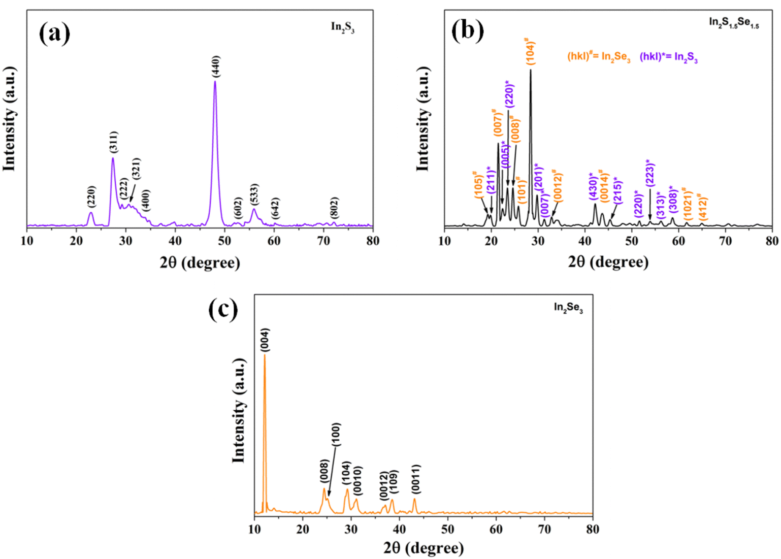 | ||
| Fig. 3 The XRD patterns of (a) In2S3, (b) In2S1.5Se1.5, and (c) In2Se3 nanostructures. | ||
3.3. Scanning electron microscopy (SEM)
The morphology of the In2S3, In2S1.5Se1.5 and In2Se3 nanostructures is depicted in Fig. 4. Fig. 4(a) shows the FESEM image of In2S3, revealing the presence of nanostructures with an average size ranging from 700 nm to 2500 nm. The size distribution of the nanostructures is displayed in Fig. 4(b). Some of the nanostructures exhibit cubic shapes, as shown in the inset of Fig. 4(a). On the other hand, Fig. 4(c) displays the FESEM image of In2S1.5Se1.5, indicating the presence of nanostructures and nanoplates. The formation of In2S1.5Se1.5 nanostructures and nanoplates may be attributed to the combination of In2S3 and In2Se3 nanostructures, which is supported by the mixed phase observed in the XRD profile of In2S1.5Se1.5. The width of some nanoplates is around 1250 nm, as shown in the inset of Fig. 4(c). The size distribution of the nanoplates is depicted in Fig. 4(d). Furthermore, EDS mapping of In2S3 and In2S1.5Se1.5 nanostructures is shown in Fig. S2 (ESI†). In contrast, the FESEM image of In2Se3 shows a nanofiber morphology as shown in Fig. 4(e). The length of a single nanofiber is approximately 3660 nm, and the width is around 139 nm. The average width distribution of the nanofibers is presented in Fig. 4(f). These nanofiber morphologies enhance the performance of the photodetector due to their large surface area. Additionally, the EDS mapping of the In2Se3 nanofibers confirms the successful presence of indium and selenium elements within the nanofiber structure, as shown in Fig. 4(g).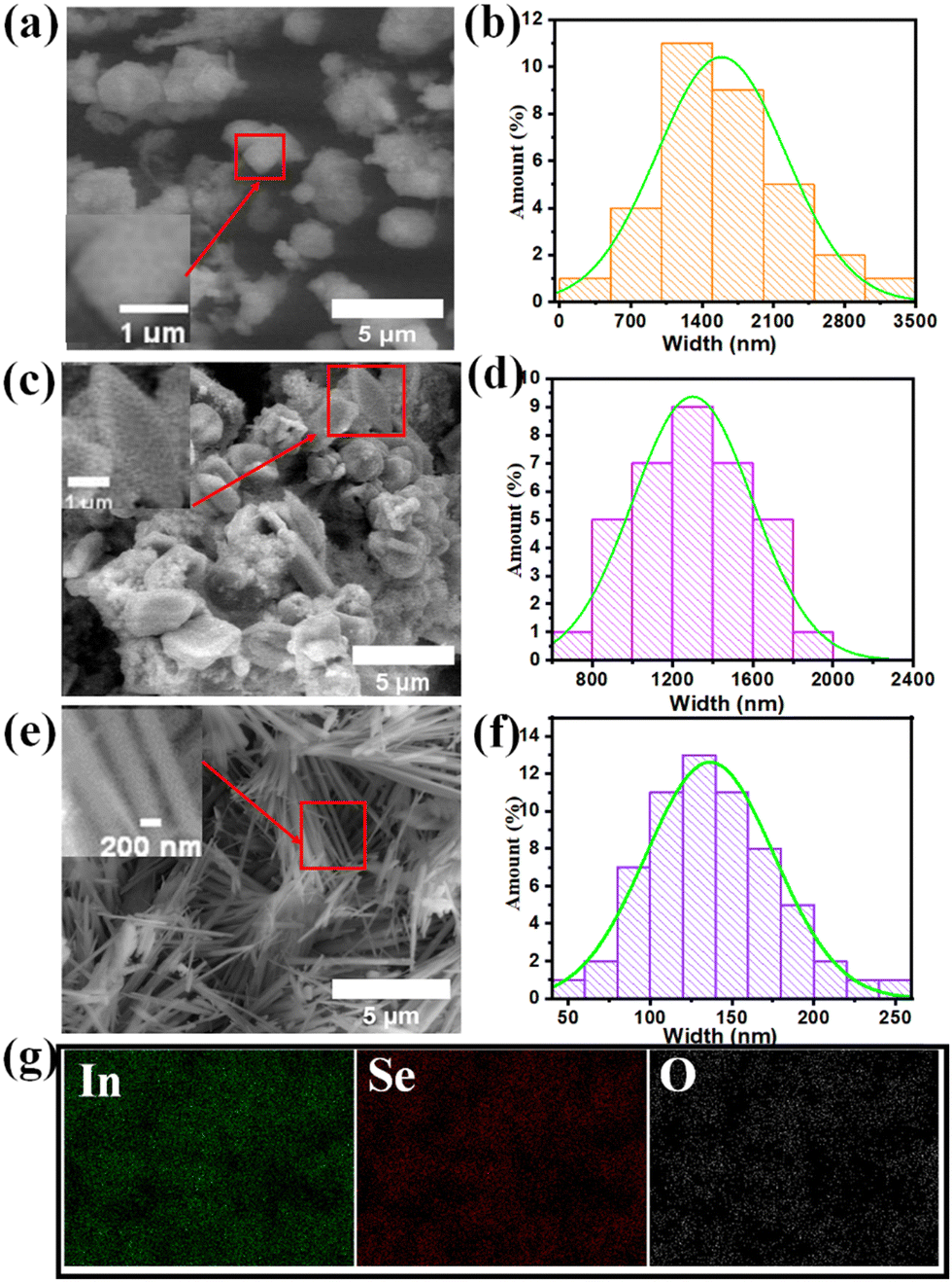 | ||
| Fig. 4 Surface morphology and size distribution analysis of (a) and (b) In2S3 nanostructures, (c) and (d) In2S1.5Se1.5 nanostructures and nanoplates, and (e) and (f) In2Se3 nanofibers, and (g) EDS mapping of In2Se3 nanofibers. | ||
3.4. Energy dispersive spectroscopy (EDS)
EDS is a reliable and effective technique for identifying elemental composition in nanostructures.59–62 The EDS spectra of the as-synthesized nanostructures are shown in Fig. S3 (ESI†). Compared to the In2S1.5Se1.5 and In2Se3 nanostructures, the amount of In in the as-synthesized In2S3 is slightly higher, according to the data analysis. In general, they are nearly stoichiometric. The absence of any other peaks in the spectra is strong evidence that the synthesised nanostructures are chemically pure.3.5. Photo detection application
To study the photo-detection applications of In2S3, In2S1.5Se1.5 and In2Se3 nanostructures separately, a glass substrate is used and the channel is prepared by making thin and straight marks using a glass cutter. Then, the suspensions of In2S3, In2S1.5Se1.5 and In2Se3 nanomaterials are drop-casted multiple times on a channel with continuous heating at 100 °C to remove the dispersing medium (distilled water). Two copper wires are bonded on the prepared samples using Ag paste. The prepared devices were further annealed at 120 °C for 5 h and used for photo-detection experiments. The various temporal detecting experiments are performed using a Keithley-4205 SMU.First, as shown in Fig. 5(a), the current–voltage characteristics of the devices were measured. The I–V curves for the devices are linear, indicating that the connections between the nanostructures and the Ag electrodes are ohmic. The current is found to increase as Se replaces S. In order to examine the transient photoresponse of the prepared devices, the light is turned on and off at regular intervals. At a bias voltage of 1 mV and under white light with a power intensity of 10 mW cm−2, the device's current is plotted as a function of time in Fig. 5(b). The devices had a consistent and reliable response to white light. Time constants are calculated for both the current rise (τrise - the time needed for the current to increase by 90%) and decay (τdecay - the time needed for the current to decrease by 10%). In addition to these, the photocurrent (Iph = IillIdark, where Iill is the current under illumination and Idark is the current in the dark) appears to be amplified from 2 μA for pure In2S3 to 70 μA (35 times) for the In2Se3 sample. The photoresponse of the In2Se3 nanofibers under different illumination intensity (10, 20, 50 and 100 mW cm−2) is shown in Fig. 5(c). A detailed photodetection study of In2Se3 device was carried out with different illumination sources. Fig. 5(d) shows the wavelength dependent pulse-photo response, examined at 485 nm, 560 nm and 670 nm light sources at intensity 5 mW cm−2 and bias voltage 1 mV. The good response at 670 nm illumination is due to the maximum optical absorbance for the In2Se3 nanofiber device.63 In contrast, nanofibers have a larger surface area-to-volume ratio than nanostructures, which can enhance the absorption of incident light and increase the number of charge carriers generated. This can lead to a higher photocurrent and sensitivity in photodetection. The detector parameters utilised in the quantitative study, including photo-responsivity, detectivity, EQE (%), rise time, and decay time at specific conditions are listed in Table 1. They are evaluated using standard equations reported by Zhou J et al.50 A comparison of the reported photodetection parameters is provided in Table 1.
 | ||
| Fig. 5 The (a) I–V characteristics, (b) pulse photoresponse of In2S3, In2S1.5Se1.5, and In2S3 nanostructures, (c) pulse photoresponse of In2Se3 nanofibers at different illumination, and (d) pulse photoresponse of In2Se3 nanofibers at different intensity. | ||
| Sample | Illumination source | Intensity (mW cm−2) | Photo current (μA) | Responsivity (mA W−1) | Detectivity ×109 (Jones) | EQE (%) | Rise time (s) | Decay time (s) |
|---|---|---|---|---|---|---|---|---|
| In2S3 | White LED | 10 | 2 | 5.3 | 1.45 | — | 5.9 | 6.7 |
| In2S1.5Se1.5 | White LED | 10 | 18 | 47.7 | 9.44 | — | 5.0 | 6.2 |
| In2Se3 | White LED | 10 | 70 | 185.8 | 23.3 | — | 8.8 | 9.5 |
| White LED | 20 | 101 | 146.0 | 18.3 | — | 8.8 | 9.5 | |
| White LED | 50 | 308 | 163.5 | 20.5 | — | 8.8 | 9.5 | |
| White LED | 100 | 680 | 180.5 | 22.6 | — | 8.8 | 9.5 | |
| 485 nm LED | 5 | 6.8 | 36.0 | 2.36 | 9.22 | 8.8 | 9.5 | |
| 560 nm LED | 5 | 8.0 | 42.4 | 2.74 | 9.41 | 8.8 | 9.5 | |
| 670 nm LED | 5 | 10.1 | 53.1 | 3.46 | 9.85 | 8.8 | 9.5 | |
| Reported In2S364 | White light Bias 5 V | 100 | 100.5 | 0.59 | 0.10 | — | 3.7 | 3.7 |
| Reported few layered InSe65 | 633 nm LASER Bias 10 V | 0.28 | — | — | 54.7 | — | — | — |
1D In2Se3 nanofibers are likely to have a higher photodetector response compared to In2S3 and In2S1.5Se1.5 nanostructures due to their unique properties. One possible reason for this higher response is the morphology of the nanofibers. Nanofibers have a high surface area to volume ratio, which can increase the interaction between the material and the incident light, leading to a higher photodetector response. Another factor is the electronic properties of In2Se3. In2Se3 has a narrow bandgap, which means that it can absorb a wide range of wavelengths of light, making it a good candidate for photodetection. Additionally, In2Se3 has high carrier mobility and a long carrier lifetime, which can enhance the efficiency of charge separation and transport, leading to a higher photodetector response.
The photodetector properties of 1D In2Se3 nanofibers are studied through detectivity and responsivity. The results show that the nanofibers exhibit a detectivity of 22.6 × 10⁹ Jones. These detectivities are higher than those of other Se-based materials such as 2D layered Ta2NiSe5,66 PdSe2 flakes,67 SnS2/InSe heterostructures,68 ZrSe369 and PANI/ZnO.70 These findings suggest that 1D In2Se3 holds promise as a material for utilization in photodetector devices.
4. Conclusion
The hydrothermal method was successfully employed to deposit nanomaterials of In2S3, In2S1.5Se1.5, and In2Se3 onto glass substrates. A study was conducted to investigate the effects of semiconductors In2S3, In2S1.5Se1.5, and In2Se3 on their structural, morphological, compositional, electrical and photodetector properties. The presence of constituent elements in the In2S3, In2S1.5Se1.5, and In2Se3 was confirmed through EDS and XPS studies. The responsivity values of the In2S3, In2S1.5Se1.5, and In2Se3 photodetectors were approximately 5.31, 47.7, and 185.8 mA W−1, respectively. The highest detectivity of 23.3 × 10⁹ Jones was obtained in the In2Se3 sample. The photodetectors exhibited very short response times, ranging from 5 to 8.8 seconds. The higher photodetector response of the 1D In2Se3 nanofibers compared to In2S3 and In2S1.5Se1.5 nanostructures may be due to their larger surface area-to-volume ratio, crystal structure, and composition, and the dimensions of the nanofibers. These findings suggest that In2Se3 nanofibers have potential applications in visible-light selective photo-sensing devices.Data availability
Data will be provided upon request.Conflicts of interest
There is no conflict of interest for any author.Acknowledgements
The authors wish to acknowledge the National Dong Hwa University, Department of Physics, Hualien 97401, Taiwan, for generously offering the necessary facilities and resources for conducting this study. Furthermore, the authors would like to extend their appreciation to Sardar Patel University P.G, Department of Physics, Vallabh Vidyanagar - 388120, Gujarat, India, for providing the essential facilities and resources for the successful completion of this work.References
- A. I. Ali, M. Ibrahim and A. Hassen, New fabrication method for di-indium tri-sulfuric (In2S3) thin films, Sci. Rep., 2022, 12, 7033, DOI:10.1038/s41598-022-11107-w.
- A. J. Khimani, S. H. Chaki, R. K. Giri, R. R. Meena, R. M. Kannaujiya and M. P. Deshpande, Thermal Exploration of Sonochemically Achieved SnS2 Nanoparticles: Elemental, Structural, and Morphological Investigations of TG Residual SnS2, Chem. Thermodyn. Therm Anal., 2023, 100104, DOI:10.1016/j.ctta.2023.100104.
- R. K. Giri, M. B. Solanki, S. H. Chaki and M. P. Deshpande, The DFT study of thermoelectric properties of CuInS2: A first principle approach, IOP Conf. Ser.: Mater. Sci. Eng., 2023, 1291, 12009, DOI:10.1088/1757-899X/1291/1/012009.
- R. K. Giri, S. H. Chaki, M. S. Dave, S. R. Bharucha, A. J. Khimani and R. M. Kannaujiya, et al., First principle insights and experimental investigations of the electronic and optical properties of CuInS2 single crystals, Mater. Adv., 2023, 4, 3246–3256, 10.1039/D3MA00166K.
- S. Li, Y. Zhang, W. Yang, H. Liu and X. Fang, 2D Perovskite Sr2Nb3O10 for High-Performance UV Photodetectors, Adv. Mater., 2020, 32, 1905443, DOI:10.1002/adma.201905443.
- W. Song, J. Chen, Z. Li and X. Fang, Self-Powered MXene/GaN van der Waals Heterojunction Ultraviolet Photodiodes with Superhigh Efficiency and Stable Current Outputs, Adv. Mater., 2021, 33, 2101059, DOI:10.1002/adma.202101059.
- J. Chen, Z. Li, F. Ni, W. Ouyang and X. Fang, Bio-inspired transparent MXene electrodes for flexible UV photodetectors, Mater. Horiz., 2020, 7, 1828–1833, 10.1039/D0MH00394H.
- Z. Li, T. Yan and X. Fang, Low-dimensional wide-bandgap semiconductors for UV photodetectors, Nat. Rev. Mater., 2023, 8, 587–603, DOI:10.1038/s41578-023-00583-9.
- F. Mesa, W. Chamorro and M. Hurtado, Optical and structural study of In2S3 thin films growth by co-evaporation and chemical bath deposition (CBD) on Cu3BiS3, Appl. Surf. Sci., 2015, 350, 38–42, DOI:10.1016/j.apsusc.2015.04.032.
- Z. S. Kachhia, S. H. Chaki, R. K. Giri, Z. R. Parekh, R. M. Kannaujiya and A. B. Hirpara, et al., Thermal decomposition study of cadmium telluride (CdTe), Mater. Today Proc., 2023 DOI:10.1016/j.matpr.2023.02.240.
- S. R. Patel, S. H. Chaki, R. K. Giri, A. J. Khimani, Y. H. Vaidya and P. Thakor, et al., Pristine, Ni- and Zn-Doped CuSe Nanoparticles: An Antimicrobial, Antioxidant, and Cytotoxicity Study, ACS Appl. Bio. Mater., 2023, 6(6), 2211–2225, DOI:10.1021/acsabm.3c00090.
- R. M. Kannaujiya, S. H. Chaki, A. J. Khimani, R. K. Giri, A. B. Hirpara and Y. H. Vaidya, et al., Mechanistic Insights into Antibacterial and Anti-biofilm Activities against multidrug-resistant microbes of SnTe nanospheres synthesized by sonochemical method, Chem. Phys. Impact, 2023, 100219, DOI:10.1016/j.chphi.2023.100219.
- R. K. Giri, S. H. Chaki, A. J. Khimani and M. P. Deshpande, Mechanistic insights into transport properties of chemical vapour transport grown CuInS2 single crystal, J. Alloys Compd., 2023, 959, 170487, DOI:10.1016/j.jallcom.2023.170487.
- Y. Chen, L. Su, M. Jiang and X. Fang, Switch type PANI/ZnO core-shell microwire heterojunction for UV photodetection, J. Mater. Sci. Technol., 2022, 105, 259–265, DOI:10.1016/j.jmst.2021.07.031.
- R. K. Giri, M. Patel, D. Kumar, J. J. L. Hmar, S. H. Chaki and M. P. Deshpande, et al., CuInS2 Nanospheres and Nanowhiskers Enhancing the Electrochemical Properties of Sodium-Ion-Conducting Gel Polymer Electrolytes, ACS Appl. Nano Mater., 2024, 7, 2855–2866, DOI:10.1021/acsanm.3c05120.
- B. R. Lee and H. W. Jang, β-In2S3 as Water Splitting Photoanodes: Promise and Challenges, Electron. Mater. Lett., 2021, 17, 119–135, DOI:10.1007/s13391-020-00266-5.
- S. Mukherjee and E. Koren, Indium Selenide (In2Se3) – An Emerging Van-der-Waals Material for Photodetection and Non-Volatile Memory Applications, Isr. J. Chem., 2022, 62, e202100112, DOI:10.1002/ijch.202100112.
- D. A. Bandurin, A. V. Tyurnina, G. L. Yu, A. Mishchenko, V. Zólyomi and S. V. Morozov, et al., High electron mobility, quantum Hall effect and anomalous optical response in atomically thin InSe, Nat. Nanotechnol., 2017, 12, 223–227, DOI:10.1038/nnano.2016.242.
- M. Li, C. Y. Lin, S. H. Yang, Y. M. Chang, J. K. Chang and F. S. Yang, et al., High Mobilities in Layered InSe Transistors with Indium-Encapsulation-Induced Surface Charge Doping, Adv. Mater., 2018, 30, 1803690, DOI:10.1002/adma.201803690.
- P.-H. Ho, Y.-R. Chang, Y.-C. Chu, M.-K. Li, C.-A. Tsai and W.-H. Wang, et al., High-Mobility InSe Transistors: The Role of Surface Oxides, ACS Nano, 2017, 11, 7362–7370, DOI:10.1021/acsnano.7b03531.
- P. M. Thakor, R. J. Patel, R. K. Giri, S. H. Chaki, A. J. Khimani and Y. H. Vaidya, et al., Synthesis, Spectral Characterization, Thermal Investigation, Computational Studies, Molecular Docking, and In Vitro Biological Activities of a New Schiff Base Derived from 2-Chloro Benzaldehyde and 3,3′-Dimethyl-[1,1′-biphenyl]-4,4′-diamine, ACS Omega, 2023, 8, 33069–33082, DOI:10.1021/acsomega.3c05254.
- F. Xue, J. Zhang, W. Hu, W.-T. Hsu, A. Han and S.-F. Leung, et al., Multidirection Piezoelectricity in Mono- and Multilayered Hexagonal α-In2Se3, ACS Nano, 2018, 12, 4976–4983, DOI:10.1021/acsnano.8b02152.
- M. S. Claro and S. Sadewasser, van der Waals Epitaxy of Ultrathin β-In2Se3 on Insulators Used in Standard Silicon Microelectronics Technology, Cryst. Growth Des., 2021, 21, 5268–5274, DOI:10.1021/acs.cgd.1c00599.
- J. Cui, H. Peng, Z. Song, Z. Du, Y. Chao and G. Chen, Significantly Enhanced Thermoelectric Performance of γ-In2Se3 through Lithiation via Chemical Diffusion, Chem. Mater., 2017, 29, 7467–7474, DOI:10.1021/acs.chemmater.7b02467.
- S. Siol, T. P. Dhakal, G. S. Gudavalli, P. P. Rajbhandari, C. DeHart and L. L. Baranowski, et al., Combinatorial Reactive Sputtering of In2S3 as an Alternative Contact Layer for Thin Film Solar Cells, ACS Appl. Mater. Interfaces, 2016, 8, 14004–14011, DOI:10.1021/acsami.6b02213.
- F. Horani and E. Lifshitz, Unraveling the Growth Mechanism Forming Stable γ-In2S3 and β-In2S3 Colloidal Nanoplatelets, Chem. Mater., 2019, 31, 1784–1793, DOI:10.1021/acs.chemmater.9b00013.
- R. B. Jacobs-Gedrim, M. Shanmugam, N. Jain, C. A. Durcan, M. T. Murphy and T. M. Murray, et al., Extraordinary Photoresponse in Two-Dimensional In2Se3 Nanosheets, ACS Nano, 2014, 8, 514–521, DOI:10.1021/nn405037s.
- B. Eghbalifar, H. Izadneshan, G. Solookinejad and L. Separdar, Investigating In2S3 as the buffer layer in CZTSSe solar cells using simulation and experimental approaches, Solid State Commun., 2022, 343, 114654, DOI:10.1016/j.ssc.2022.114654.
- C.-H. Ho, M.-H. Lin, Y.-P. Wang and Y.-S. Huang, Synthesis of In2S3 and Ga2S3 crystals for oxygen sensing and UV photodetection, Sens. Actuators, A, 2016, 245, 119–126, DOI:10.1016/j.sna.2016.05.003.
- B. Bouricha, R. Souissi, N. Bouguila and A. Labidi, A real-time sharp selectivity with In2S3 gas sensor using a nonlinear dynamic response for VOCs, Measurement, 2021, 185, 110070, DOI:10.1016/j.measurement.2021.110070.
- Y. Zhao, F. Guo, R. Ding, W. F. Io, S.-Y. Pang and W. Wu, et al., Piezo-Phototronic Effect in 2D α-In2Se3/WSe2 van der Waals Heterostructure for Photodetector with Enhanced Photoresponse, Adv. Opt. Mater., 2021, 9, 2100864, DOI:10.1002/adom.202100864.
- W. Feng, W. Zheng, G. Feng, X. Chen, G. Liu and T. Hasan, et al., Sensitive Electronic-Skin Strain Sensor Array Based on the Patterned Two-Dimensional α-In2Se3, Chem. Mater., 2016, 28, DOI:10.1021/acs.chemmater.6b01073.
- S. M. Poh, S. J. R. Tan, H. Wang, P. Song, I. H. Abidi and X. Zhao, et al., Molecular-Beam Epitaxy of Two-Dimensional In2Se3 and Its Giant Electroresistance Switching in Ferroresistive Memory Junction, Nano Lett., 2018, 18, 6340–6346, DOI:10.1021/acs.nanolett.8b02688.
- J. Li, H. Li, X. Niu and Z. Wang, Low-Dimensional In2Se3 Compounds: From Material Preparations to Device Applications, ACS Nano, 2021, 15, 18683–18707, DOI:10.1021/acsnano.1c03836.
- B. Hemanth Kumar, S. Shaji and M. C. Santhosh Kumar, Fabrication of visible light photodetector using co-evaporated Indium Sulfide thin films, J. Mater. Sci.: Mater. Electron., 2019, 30, 17986–17998, DOI:10.1007/s10854-019-02152-9.
- Y. Li, Q. Wang, Y. Gao, B. Liu, C. Gao and Y. Ma, Investigation on morphological properties of In2S3 by high pressure X-ray diffraction, Mater. Res. Express, 2017, 4, 85902, DOI:10.1088/2053-1591/aa8002.
- J. Zhao and L. Yang, Structure Evolutions and Metallic Transitions in In2Se3 Under High Pressure, J. Phys. Chem. C, 2014, 118, 5445–5452, DOI:10.1021/jp4076383.
- M. Küpers, P. M. Konze, A. Meledin, J. Mayer, U. Englert and M. Wuttig, et al., Controlled Crystal Growth of Indium Selenide, In2Se3, and the Crystal Structures of α-In2Se3, Inorg. Chem., 2018, 57, 11775–11781, DOI:10.1021/acs.inorgchem.8b01950.
- Y. Chi, Z.-D. Sun, Q.-T. Xu, H.-G. Xue and S.-P. Guo, Hexagonal In2Se3: A Defect Wurtzite-Type Infrared Nonlinear Optical Material with Moderate Birefringence Contributed by Unique InSe5 Unit, ACS Appl. Mater. Interfaces, 2020, 12, 17699–17705, DOI:10.1021/acsami.9b23085.
- H. Peng, D. T. Schoen, S. Meister, X. F. Zhang and Y. Cui, Synthesis and Phase Transformation of In2Se3 and CuInSe2 Nanowires, J. Am. Chem. Soc., 2007, 129, 34–35, DOI:10.1021/ja067436k.
- L.-Y. Chen, Z.-D. Zhang and W.-Z. Wang, Self-Assembled Porous 3D Flowerlike β-In2S3 Structures:
![[thin space (1/6-em)]](https://www.rsc.org/images/entities/char_2009.gif) Synthesis, Characterization, and Optical Properties, J. Phys. Chem. C, 2008, 112, 4117–4123, DOI:10.1021/jp710074h.
Synthesis, Characterization, and Optical Properties, J. Phys. Chem. C, 2008, 112, 4117–4123, DOI:10.1021/jp710074h. - G. Cao, Y. Zhao and Z. Wu, Synthesis and characterization of In2S3 nanoparticles, J. Alloys Compd., 2009, 472, 325–327, DOI:10.1016/j.jallcom.2008.04.047.
- X. Li, Y. Han, Z. Shi, M. An, E. Chen and J. Feng, et al., β-In2S3 Nanoplates for Ultrafast Photonics, ACS Appl. Nano Mater., 2022, 5, 3229–3236, DOI:10.1021/acsanm.1c03542.
- Q. Shen, S. Zhou, F.-L. Yang, X. Wang and X. Han, Engineering one-dimensional hollow beta-In2S3/In2O3 hexagonal micro-tubes for efficient broadband-light photocatalytic performance, J. Mater. Chem. A, 2022, 10, 4974–4980, 10.1039/D2TA00083K.
- S. Kumar and T. T. John, Highly photo-responsive In2S3 thin film by sulfurizing indium layer, Mater. Chem. Phys., 2022, 286, 126222, DOI:10.1016/j.matchemphys.2022.126222.
- P. Hu, Y. Xin, C. Yao and Y. Miao, In2S3/BiOI composites boost visible-light photocatalytic degradation of tetracycline hydrochloride, CrystEngComm, 2021, 23, 3488–3497, 10.1039/D1CE00134E.
- A. Timoumi, W. Belhadj, S. N. Alamri and M. K. Al-Turkestani, Physical and Dielectric Properties of Ni-Doped In2S3 Powders for Optical Windows in Thin Film Solar Cells, Mater, 2021, 14, DOI:10.3390/ma14195779.
- M. D. Sharma and M. Basu, Nanosheets of In2S3/S-C3N4-Dots for Solar Water-Splitting in Saline Water, Langmuir, 2022, 38, 12981–12990, DOI:10.1021/acs.langmuir.2c02390.
- R. Li, L. Tang, Q. Zhao, T. H. Ly, K. S. Teng and Y. Li, et al., In2S3 Quantum Dots: Preparation, Properties and Optoelectronic Application, Nanoscale Res. Lett., 2019, 14, 161, DOI:10.1186/s11671-019-2992-0.
- S. Ramya, D. Nataraj, S. Krishnan, S. Premkumar, T. Thrupthika and A. Sangeetha, et al., Aggregation induced emission behavior in oleylamine acetone system and its application to get improved photocurrent from In2S3 quantum dots, Sci. Rep., 2020, 10, 19712, DOI:10.1038/s41598-020-76703-0.
- Y. Liu, H. Xu and Y. Qian, Double-Source Approach to In2S3 Single Crystallites and Their Electrochemical Properties, Cryst. Growth Des., 2006, 6, 1304–1307, DOI:10.1021/cg0504298.
- W. Rehwald and G. Harbeke, On the conduction mechanism in single crystal β-indium sulfide In2S3, J. Phys. Chem. Solids, 1965, 26, 1309–1324, DOI:10.1016/0022-3697(65)90114-9.
- J. Zhou, G. Tian, Y. Chen, Y. Shi, C. Tian and K. Pan, et al., Growth rate controlled synthesis of hierarchical Bi2S3/In2S3 core/shell microspheres with enhanced photocatalytic activity, Sci. Rep., 2014, 4, 4027, DOI:10.1038/srep04027.
- L. Liu, J. Dong, J. Huang, A. Nie, K. Zhai and J. Xiang, et al., Atomically Resolving Polymorphs and Crystal Structures of In2Se3, Chem. Mater., 2019, 31, 10143–10149, DOI:10.1021/acs.chemmater.9b03499.
- G. Almeida, S. Dogan, G. Bertoni, C. Giannini, R. Gaspari and S. Perissinotto, et al., Colloidal Monolayer β-In2Se3 Nanosheets with High Photoresponsivity, J. Am. Chem. Soc., 2017, 139, 3005–3011, DOI:10.1021/jacs.6b11255.
- K. Wang, Z. Zhang, T. Cheng, Z. Xing, Z. Li and W. Zhou, Hollow core–shell Co9S8@In2S3 nanotube heterojunctions toward optimized photothermal–photocatalytic performance, Catal. Sci. Technol., 2021, 11, 7412–7419, 10.1039/D1CY01637G.
- Y. Qin, Z. Jiang, L. Guo, J. Huang, Z.-J. Jiang and M. Liu, Sulfurization synthesis of a new anode material for Li-ion batteries: understanding the role of sulfurization in lithium ion conversion reactions and promoting lithium storage performance, J. Mater. Chem. A, 2019, 7, 21270–21279, 10.1039/C9TA08394D.
- J. Feng, S. Luo, S. Yan, Y. Zhan, Q. Wang and Y. Zhang, et al., Hierarchically nitrogen-doped carbon wrapped Ni0.6Fe0.4Se2 binary-metal selenide nanocubes with extraordinary rate performance and high pseudocapacitive contribution for sodium-ion anodes, J Mater Chem A, 2021, 9, 1610–1622, 10.1039/D0TA08423A.
- S. A. Kadam, Y.-R. Ma, Y.-R. Chen, Y. H. Navale, A. S. Salunkhe, V. B. Patil, S. D. Ralegankar and P. D. More, Mn-Incorporated α-Fe2O3 Nanostructured Thin Films: Facile Synthesis and Application as a High-Performance Supercapacitor, J. Electron. Mater., 2023, 52, 500–513, DOI:10.1007/s11664-022-10019-9.
- P. More, S. A. Kadam, Y.-R. Ma, Y.-R. Chen, N. Tarwal, Y. Navale, A. Salunkhe and V. Patil, Spray Synthesized Mn-doped CuO Electrodes for High Performance Supercapacitor, ChemistrySelect, 2022, 7, e202202504, DOI:10.1002/slct.202202504.
- S. A. Thomas, S. A. Kadam, Y.-R. Ma and A. Aravind, Photocatalytic Degradation of Malachite Green Dye Using Zinc Sulfide Nanostructures, ChemistrySelect, 2021, 6, 10015–10024, DOI:10.1002/slct.202102109.
- N. S. George, S. Anil Kadam, S. Sreehari, L. Maria Jose, Y. Ron Ma and A. Aravind, Inquest on photocatalytic and antibacterial traits of low composition Cu doped ZnO nanoparticles, Chem. Phys. Lett., 2023, 815, 140351, DOI:10.1016/j.cplett.2023.140351.
- X. F. Wei, L. W. Li, H. G. Feng, J. B. Gong, K. Jiang and S. L. Xue, Preparation and optical properties of In2Se3 nanospheres using CTAB as surface modifier, Ceram. Int., 2020, 46, 1026–1032, DOI:10.1016/j.ceramint.2019.09.067.
- B. Hemanth Kumar and M. C. Santhosh Kumar, Indium sulfide based metal-semiconductor-metal ultraviolet-visible photodetector, Sens. Actuators, A, 2019, 299, 111643, DOI:10.1016/j.sna.2019.111643.
- S. R. Tamalampudi, Y.-Y. Lu, U. Rajesh Kumar, R. Sankar, C.-D. Liao, B. Karukanara Moorthy, C.-H. Cheng, F. C. Chou and Y.-T. Chen, High Performance and Bendable Few-Layered InSe Photodetectors with Broad Spectral Response, Nano Lett., 2014, 14, 2800–2806, DOI:10.1021/nl500817g.
- Y. Zhang, W. Yu, J. Li, J. Chen, Z. Dong and L. Xie, et al., Ultra-broadband photodetection based on two-dimensional layered Ta2NiSe5 with strong anisotropy and high responsivity, Mater. Des., 2021, 208, 109894, DOI:10.1016/j.matdes.2021.109894.
- Q. Liang, Q. Wang, Q. Zhang, J. Wei, S. X. Lim and R. Zhu, et al., High-Performance, Room Temperature, Ultra-Broadband Photodetectors Based on Air-Stable PdSe2, Adv. Mater., 2019, 31, e1807609, DOI:10.1002/adma.201807609.
- S. Hosseini, A. Iraji Zad, S. M. Mahdavi and A. Esfandiar, Tunable Gain SnS2/InSe van der Waals Heterostructure Photodetector, Micromachines, 2022, 13, DOI:10.3390/mi13122068.
- X. Wang, T. Xiong, K. Xin, J. Yang, Y. Liu and Z. Zhao, Polarization sensitive photodetector based on quasi-1D ZrSe3, J. Semicond., 2022, 43, 102001, DOI:10.1088/1674-4926/43/10/102001.
- Y. Chen, L. Su, M. Jiang and X. Fang, Switch type PANI/ZnO core-shell microwire heterojunction for UV photodetection, J. Mater. Sci. Technol., 2022, 105, 259–265, DOI:10.1016/j.jmst.2021.07.031.
Footnote |
| † Electronic supplementary information (ESI) available. See DOI: https://doi.org/10.1039/d3ma00808h |
| This journal is © The Royal Society of Chemistry 2024 |