
 Open Access Article
 This Open Access Article is licensed under a
 Creative Commons Attribution 3.0 Unported Licence
Gate-controlled rectification and broadband photodetection in a P–N diode based on TMDC heterostructures†
Ehsan
Elahi‡
 *a,
Sobia
Nisar‡
bc,
Muhammad
Rabeel
bc,
Malik Abdul
Rehman
d,
Mohamed
Ouladsamne
e,
Ahmad
Irfan
f,
Muhammad
Abubakr
bg,
Jamal
Aziz
h,
Muhammad
Asim
a and
Ghulam
Dastgeer
*a
*a,
Sobia
Nisar‡
bc,
Muhammad
Rabeel
bc,
Malik Abdul
Rehman
d,
Mohamed
Ouladsamne
e,
Ahmad
Irfan
f,
Muhammad
Abubakr
bg,
Jamal
Aziz
h,
Muhammad
Asim
a and
Ghulam
Dastgeer
*a
aDepartment of Physics & Astronomy, Sejong University, Seoul, 05006, South Korea. E-mail: Ehsanelahi@sju.ac.kr; gdastgeer@sejong.ac.kr
bDepartment of Electrical Engineering, Sejong University, 209 Neungdong-ro, Gwangjin-gu, Seoul, 05006, South Korea
cDepartment of Convergence Engineering for Intelligent Drone, Sejong University, Seoul, 05006, South Korea
dDepartment of Chemical Engineering, New Uzbekistan University, Tashkent, 100007, Uzbekistan
eDepartment of Chemistry, College of Science, King Saud University, Riyadh, 11451, Saudi Arabia
fDepartment of Chemistry, College of Science, King Khalid University, Abha 61413, P.O. Box 9004, Saudi Arabia
gGraduate School of Optical Engineering, Sejong University, Seoul, 05006, South Korea
hSchool of Electrical, Information and Media Engineering, Bergische Universität Wuppertal, Lise-Meitner-Straße 13, Wuppertal 42119, Germany
First published on 14th December 2023
Abstract
van der Waals (vdW) heterostructures in two dimensions have electrical and optoelectronic characteristics that make them a suitable platform for the creation of sophisticated nanoscale electronic devices. Outstanding p–n heterojunctions made of two-dimensional atomic layers are essential for the realization of superior integrated optoelectronics. This article shows how WSe2 and SnS2 layers are stacked by vdW heterostructures to build a p–n junction diode over Si/SiO2 substrates; Raman mapping confirms the heterostructure even further. The WSe2/SnS2 vdW heterostructure's electrical attributes show ultra-low dark currents because of the junction's depletion area and robust direct current passage when lit. An energy band diagram is also used to study and describe the charge transport process. When the back-gate voltage is swept effectively, 2.9 × 10⁴ is the rectification ratio (RR). The photovoltaic characteristics of the WSe2/SnS2 heterostructure have been studied under irradiation of light with different wavelengths (λ). When 220 nm light is applied to the WSe2/SnS2 vdW heterostructure, a change in the photocurrent of 65 nA is observed. Under light irradiation of deep ultraviolet (DUV) light at λ = 220 nm and Vds = 0.5 V, the device revealed a responsivity (R) of 1.31 × 10⁵ m AW−1, with a substantial EQE of 7.3 × 10⁴ (%) and a detectivity (D*) of around 3.13 × 10¹⁰ Jones. The creation of these superior p–n junctions opens the door for the production of logical and effective optoelectronic devices.
1. Introduction
van der Waals (vdW) heterostructures based on atomically thin 2D materials have ushered in a new era in next-generation electronics and optoelectronics. This is a result of the ultrathin morphological features and the unique energy band alignments.1–7 As opposed to typical semiconductor heterojunctions, these vdW heterostructures enable the development of configurations without the restriction of atomic lattice match and have high-quality integrations since there are no dangling bonds at the interfaces.8,9 These ultrathin vdW nanostructures have demonstrated potential performance for light-emitting diodes (LEDs),10 field effect transistors (FETs),11,12 logic circuits,13 photodetectors,14–16 flexible devices,17 and bipolar junction transistors.5 In particular, 2D transition metal dichalcogenides (TMDCs)18–21 are composed of an ordered stacking of building blocks and have a high carrier mobility22,23 and numerous spin characteristics.24–27 The most prevalent and essential p–n junctions are essential parts of optoelectronic and semiconductor devices. Since the development of atomically thin vdW 2D materials, a multitude of heterostructure-based p–n junctions have been created.3,28 However, the majority of prior research used extra procedures that produced p-type TMDCs, such as chemical doping, special metal contact, and electrical gating methods for developing p–n junctions, which have challenging and disruptive factors for vdW p–n junction practical applications.29,30 Stacking individual layers of different 2D materials in a vdW heterostructure allows for the customization of energy band alignment and creates atomically sharp surfaces. This presents numerous opportunities for fundamental research into novel electrical and optical properties. As a result, most of the current investigations in the field of 2D TMDCs have been on TMDCs/TMDCs or TMDCs/graphene heterostructures.3,31 Various TMDC-based heterostructures with diode rectification and photovoltaic properties have previously been described, including p-MoS2/n-MoS2,32 ReSe2/ReS2,33 and MoS2/BP.28 However, WSe2/MoS2 heterojunctions also exhibit a gate-tunable photovoltaic response,3,34 and photovoltaic photodetectors utilizing MoTe2/MoS2 vdW heterojunctions are also revealed.35,36 Due to the inadequate photocurrent flow without an external bias impact, these mentioned photovoltaic devices still have a poor response (< 0.5 A W−1). To enhance the functionality of photovoltaic photodetectors based on TMDCs for upcoming nanoscale optoelectronic devices, further work is required.Tin disulfide (SnS2), a 2D material with an unusual band structure that is a IV–VI semiconductor with each layer of Sn atoms sandwiched between two layers of S atoms, interacts with other layers via vdW interactions. SnS2, a significant n-type layered semiconductor, has garnered considerable interest due to its affordability, abundance on earth, non-toxicity, and environmental sustainability.37 SnS2 is intensively investigated in its bulk form, primarily for photovoltaics.38 SnS2 is an intriguing 2D TMDC because of its high carrier mobility39,40 and potent excitonic effect (0.9 eV binding energy for a single layer).41 2D nanostructures combining p-type WSe2 and n-type SnS2 have recently attracted a great deal of attention. Zhang et al. showed the growth of a few layers of WSe2 on randomly oriented SnS2 microplates.42
In this study, we present the successful fabrication of WSe2/SnS2 van der Waals p–n junctions on a Si/SiO2 substrate using the mechanical exfoliation technique. The two-dimensional nature of WSe2 and SnS2 allowed for a high-quality van der Waals heterostructure to be obtained, resulting in a p–n junction with an atomically sharp junction. The electrical characteristics of the WSe2/SnS2 vdW heterostructure are studied at various back-gate voltages varying from −60 to +60 V. The WSe2/SnS2 van der Waals heterostructure exhibited a suitable rectification ratio (RR) of 2.9 × 10⁴, which indicates a reliable switching behavior. Additionally, the devices displayed a low leakage current and a fast photoresponse, making them well-suited for optoelectronic applications. The photoresponse of the devices was studied under illumination with various wavelengths of light. The measured photocurrent (Iph) change was approximately 65 nA, revealing the excellent sensitivity of the fabricated p–n junction to the incident light (DUV). Furthermore, the device indicated a responsivity (R) of 1.31 × 10⁵ mA W−1 with a significant external quantum efficiency (EQE) of 7.3 × 10⁴ (%) and a detectivity (D*) of about 3.13 × 10¹⁰ Jones. This value suggests that the fabricated devices are capable of converting a high percentage of incident photons into electrical currents, making them ideal for use in energy-harvesting applications. The excellent photoresponse of the WSe2/SnS2 p–n junction under DUV light could be attributed to the efficient light absorption, built-in electric field, and high carrier mobility and the clean interface of the materials. The development of these van der Waals heterostructures represents a significant step forward in the design of high-performance integrated optoelectronic systems and products.
2. Device fabrication
A conventional dry transfer technique was adopted to build the WSe2/SnS2 vdW heterojunction device. Thin flakes of SnS2 were initially exfoliated from the bulk (HQ graphene company) using scotch tape and then transferred onto a Si/SiO2 substrate. Then, a few layers of WSe2 were exfoliated onto PDMS and relocated onto a thin film of SnS2 using an aligned transfer system under an optical microscope. The electrode was designed by the electron-beam lithography technique (EBL/SEM), and Cr/Au (5/60 nm) metal electrodes were deposited using a thermal evaporation system to fabricate the device for measurements. An optical microscope was used to examine the morphology of the vdW heterostructure based on WSe2/SnS2. An atomic force microscope was used to measure the thickness. Electrical measurements were performed using a Keithley system in a high vacuum environment at room temperature.2.1. Results and discussion
The graphic illustration of the device based on the heterostructure WSe2–SnS2 p–n diode is demonstrated in Fig. 1(a). Fig. 1(b) shows the optical representation of the device-based WSe2/SnS2 vdW heterostructure with metal electrodes placed on the flakes. Fig. 1(c) shows the SEM image of the device. Fig. 1(d) and (e) points to the atomic force microscopy (AFM) image and profile height of the heterojunction WSe2–SnS2 of the p–n device. The thickness of the heterostructure WSe2–SnS2 is ≈12 nm. The individual thickness and AFM images of WSe2 and SnS2 flakes are illustrated in Fig. S1(a) and (b), ESI.† Raman spectroscopy is a power tool to characterize the material, two strong peaks of WSe2 may be seen at 259 cm−1 (A1g, out-of-plane mode), and 247 cm−1 (E12g, in-plane mode), and SnS2 has only one major peak (A1g, out-of-plane) at 310 cm−1 as shown in Fig. 1(f). The specific Raman spectra of both materials are seen in Fig. S2(a) and (b), ESI.† | ||
| Fig. 1 (a) Graphical representation of the p–n device based on WSe2–SnS2 heterojunctions. (b) Optical image of the device that contains the flakes and metal electrodes. (c) SEM image of the device, and the scale bar is 2 μm. (d) AFM image of the device. (e) Height profile of the heterostructure. (f) Raman spectroscopy of the heterostructure WSe2–SnS2. | ||
Raman intensity maps need an extensive understanding of the vdW heterostructure, material parameters, and Raman spectroscopy. To see how they were distributed spatially within the heterostructure, we checked intensity maps. The WSe2 and SnS2 grains are now perfectly cleaved laterally in the heterostructure avoiding the formation of alloy layers at their junction, as seen by the Raman intensity of WSe2/SnS2. In Fig. 1(b), the region chosen for Raman mapping investigation is outlined by yellow dashed lines. The graphical interpretation of the Raman intensity mapping of E12g and A1g for WSe2, and A1g for SnS2 is shown in Fig. 2(a) and (c). The dark spaces in the figures show the placement of Cr/Au contacts and the space of the heterostructure of both materials. These Raman intensity maps show the appropriate heterostructure developed by both materials WSe2 and SnS2.
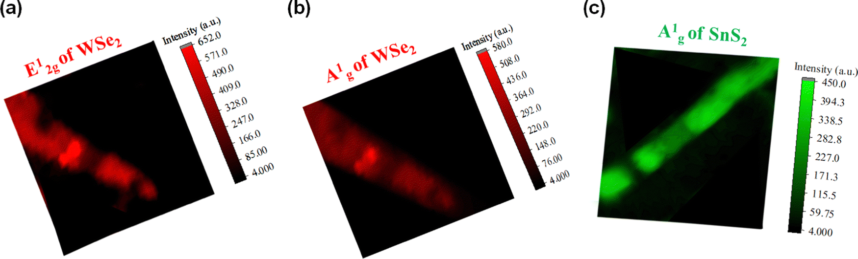 | ||
| Fig. 2 Raman mapping for the heterostructure WSe2–SnS2. (a) Intensity maps of WSe2 (E12g) and (b) A1g of WSe2. (c) Raman intensity map of SnS2 (A1g). | ||
The I–V curve of WSe2 with a back-gate voltage is presented in Fig. 3(a), which shows a nonlinear curve due to the non-ohmic contact of Au/WSe2. The I–V curve of SnS2 with a back-gate voltage is represented in Fig. 3(b), which represents the linear curve due to the ohmic contact of Au/SnS2. The transfer curves of WSe2 with respect to back-gate voltages at Vds = 0.2 V and 1 V are illustrated in Fig. 3(c), which demonstrates the dominant p-type behavior of WSe2. Fig. 3(d) displays the transfer curves of SnS2 with respect to the back-gate voltages at Vds = 0.5 V and 1 V, which shows the dominant n-type behavior.
 | ||
| Fig. 3 (a) I–V curve of the multilayer flake of WSe2, at different back-gate voltages (Vbg). (b) I–V curves of the multilayer SnS2 flake at different back-gate voltages (Vbg). (c) The transfer curve of the WSe2 flake clearly shows the dominant p-type behavior. (d) Transfer curves of SnS2 show the n-type behavior. | ||
Additionally, the back-gate voltage (Vbg) was applied to measure the rectification characteristics of the WSe2/SnS2 vdW heterojunction diode. Fig. 4(a) illustrates the charge transport across the p–n junction for various Vbg, and the maximum value of source–drain current is 47 μA. A p–n diode forms across the heterojunction, according to the clear current rectification behavior displayed by gate-tunable output curves. The increasing interlayer recombination is attributed to a substantial forward current (If), which may be controlled in TMDCs using Vbg (electrostatic gating) more successfully than in conventional materials. Due to the rise in the height of the potential barrier among the p-WSe2/n-SnS2 based diode, the reverse current is similarly reduced at a reverse bias (Vds < 0). Fig. 4(b) shows the logarithmic plot of I–V curves at back-gate voltages. The rectification ratio (RR = If/Ir) is the ratio of forward-bias (If) to reverse-bias current (Ir). The variation in the RR with respect to Vbg is investigated and represented in Fig. 4(c), and the maximum value of the RR is about 2.9 × 10⁴ at Vbg = −30 V. Because of the large drop in the leakage current, the magnitude of the RR is improved and adjusted more efficiently at a negative back-gate voltage (Vbg < 0 V). Because of the rise in the barrier height at a low bias, Ir is decreased more efficiently than If at Vbg < 0 V. The ideality factor, also known as the diode ideality factor, is a parameter used to describe the deviation from ideal behavior in diodes or other semiconductor devices. The ideality factor (η) was calculated for the forward-biased zone by fitting the logarithmic I–V characteristics to the Shockley diode equation.
 | (1) |
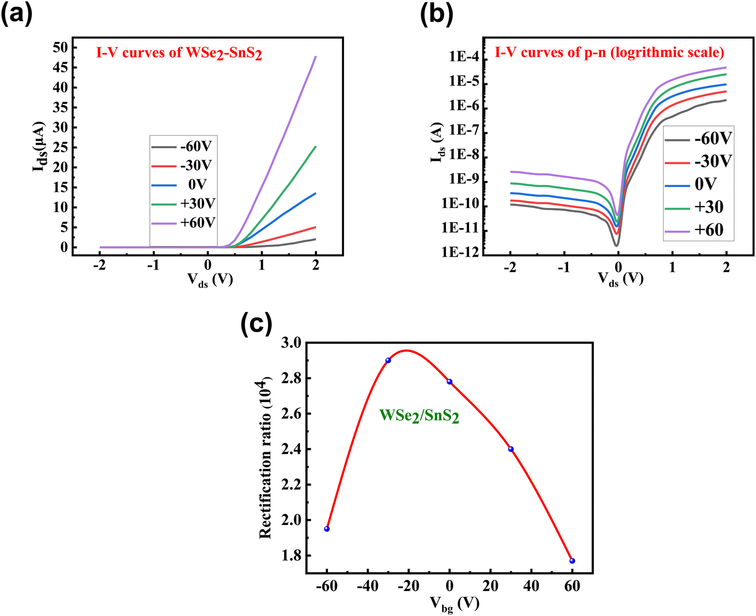 | ||
| Fig. 4 (a) I–V characteristic curves of the heterostructure WSe2–SnS2 based p–n junction at various back-gate voltages. (b) I–V characteristic curve (logarithmic scale) of the p–n junction at different Vbg. (c) Change in the rectification ratio with respect to Vbg. | ||
Fig. 5(a) shows the energy-band diagram with the work function, WSe2 and SnS2, conduction band minima, and valence band maxima. The band structure, carrier concentration, bandgap, device functioning, and optical features of a solid material, especially a semiconductor or an insulator, may all be understood from an energy band diagram. By understanding the energy levels and the occupancy of the bands, one can determine the availability of charge carriers and their behavior under different conditions, such as at equilibrium or under biasing.43 For WSe2, the Fermi level is close to the valence band, which exhibits p-type behavior, while in the case of SnS2, it is close to the conduction band, which exhibits n-type behavior. The band diagram of the WSe2/SnS2 vdW heterostructure diode following contact at zero Vbg, in which the Fermi level is positioned, is shown in the first section of Fig. 5(b). The zoom-in picture of the band alignment following the contact at zero Vbg is shown in the second section. As WSe2 is the p-type semiconductor which will conduct because of the holes. These holes are controlled via a gate voltage and a threshold in current is observed during the transfer curve as the gate voltage is increased in the negative regime from 0 to −50 V. In contrast, the carrier transport in n-type SnS2 is also regulated using the gate voltage because it conducts a high current due to electrons when the gate voltage is increased from 0 to +50 V (see Fig. 3c and d). The gate voltage plays a crucial role in controlling the charge carrier densities of holes and electrons in p-type WSe2 and n-type SnS2, respectively, and consequently influences the rectification ratio (RR). By manipulating the gate voltage, we can adjust the Fermi level. Specifically, at Vbg < 0 V, the Fermi level shifts away from the conduction band (CB), leading to an improvement in the potential barrier at the interface of the WSe2/SnS2 vdW heterojunction diode. This results in a higher rectifying current. Conversely, when the Fermi level moves toward the CB at Vbg > 0 V, the barrier height decreases, and the rectification ratio is reduced. Thus, the gate voltage serves as a powerful tool for modulating both charge carriers and band alignments in the WSe2/SnS2 vdW heterojunction diode, offering a versatile approach to designing highly efficient vdW heterostructures.
 | ||
| Fig. 5 Band diagram of a p-WSe2/n-SnS2 diode at Vbg = 0 V. (a) The band diagram of a p-WSe2/n-SnS2 diode before contact and (b) The diode after contact. | ||
3. Photoresponse assessment for WSe2/SnS2
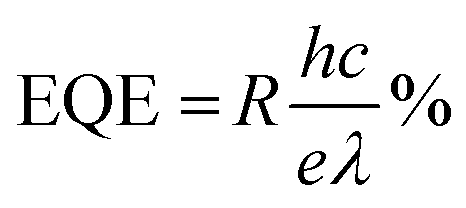
The photoresponse features of the p–n heterojunction WSe2/SnS2 were investigated using the schematic arrangement as shown in Fig. 6(a). The investigations were carried out by providing a drain voltage Vds to WSe2 (p-type, terminal “d”) and grounding SnS2 (n-type, terminal “s”). Time-resolved photoresponse experiments were done by turning on and off the laser light (220 nm, 11 mW cm−2) to study the photoresponse of the WSe2/SnS2 p–n diode. With the on/off photo-switching trend at Vds = 0.3 V and 0.5 V and no extra gate voltage, the photodetector demonstrates good stability and reliability. Iph is the photocurrent, which is defined as Iph = Iight – Idark, and the results obtained with a laser power are displayed at Vds = 0.3 V and 0.5 V in Fig. 6(b). The photocurrent (Iph) change measured was around 65 nA at Vds = 0.5. At room temperature, this device represented a short circuit current (Isc) of −8.72 nA and an open circuit voltage (Voc) of 0.15 V when Vbg = 0 as presented in Fig. 6(c). A photodetector's responsivity is a metric that measures how well it can transform incoming light into an electrical signal. It shows the connection between the photodetector's optical power input and the consequent electrical output. Responsivity (R) is computed as: | (2) |
 | (3) |
 | ||
| Fig. 6 (a) Schematic representation of the photocurrent measurement. (b) Time-dependent photoresponse of the WSe2/SnS2 p–n junction at fixed Vds = 0.3 and 0.5 V. The light is on and off after a constant interval and the photoresponse is recorded. (c) I–V curves of the WSe2/SnS2 p–n junction in the dark and under light of 220 nm at zero gate voltage. (d) Photocurrent of the device at different wavelengths of incident light. (e) Variation in R and EQE at various wavelengths of radiant light. | ||
This equation has the following metrics: the wavelength of light (λ), the charge of an electron (e), the speed of light (c), and Plank's constant (h). The EQE value is defined by light absorption and the build-up of photo-generated carriers. Detectivity (D*) is a measure of a photodetector's sensitivity, which may be calculated as D* = RA1/2/(2e*Idark)1/2, where R denotes responsivity, “A” is an operational area, e denotes the charge of electron, and Idark is the dark current.44,45 The detectivity (D*) is about 3.13 × 10¹⁰ Jones. Understanding noise mechanisms is crucial when working with photodetectors, and three major sources of noise are thermal noise, shot noise, and 1/f noise (flicker noise). Thermal noise, which is especially significant in room-temperature 2D photodetectors, is caused by the irregular thermal mobility of carriers inside the device's resistance. Shot noise is a common noise mechanism in low-light situations and arises from the discrete nature of carriers. It follows the Poisson process. Conversely, 1/f noise, often known as flicker noise, introduces random variations in the power spectral density that are inversely proportional to frequency. While its source is still up for debate, flicker noise can provide valuable information about the internal quality and reliability of a device. It is important to recognize that shot noise and heat noise appear primarily at higher frequencies.46,47
The rising and decay times were observed by fitting the data obtained through the photocurrent. The rise and decay time values are 0.52 s and 0.63 s, and the specified calculation and formula are represented in Fig. S4(a) and (b) (ESI†).
The photoresponse of the device at various wavelengths, as depicted in Fig. 6(d), reveals a decrease in the photocurrent as the wavelength of radiant light is increased. In a photodetector material, electron–hole pairs are generated when photons with sufficient energy are absorbed. The energy of photons is inversely proportional to their wavelength, as described by the equation E = hc/λ. As the wavelength increases, the energy of the incident photons decreases. For the efficient generation of electron–hole pairs and subsequent participation in the photocurrent, the energy of incident photons must be higher than the bandgap energy. When the incident photon energy is lower than the bandgap energy, fewer electron–hole pairs are formed, leading to a reduction in the photocurrent. Therefore, the observed decrease in the photocurrent with an increase in the wavelength can be attributed to the diminishing capability of photons to overcome the bandgap energy barrier and generate electron–hole pairs. This clarification aligns with the observed variations in photoresponsivity (R) and EQE, as presented in Fig. 6(e). We will incorporate this improved explanation in our revised manuscript. The logarithmic plot of the photocurrent shown in Fig. 6(b) and (d) is also presented in Fig. S5 (ESI†) to see the on and off states clearly. Consequently, the 2D-based WSe2/SnS2 heterojunction broadband photodetector developed showed tremendous promise for fast and weak signal recognition applications in integrated optoelectronics.
4 Conclusions
In conclusion, this study successfully demonstrated the fabrication of high-quality WSe2/SnS2 vdW p–n junctions on a Si/SiO2 substrate using the mechanical exfoliation technique. The resulting p–n junction exhibited an atomically sharp interface, which allows for reliable switching behavior, as demonstrated by a suitable rectification ratio (RR) of 2.9 × 10⁴. The devices also displayed a low leakage current and a rapid photo response, making them well-suited for use in optoelectronic applications. We observed the photoresponse of the device in a broadband range with radiant light which is illuminated at various wavelengths. Under λ = 220 nm (illumination), the devices exhibited high sensitivity to incident light, as demonstrated by the measured photocurrent (Iph) change of approximately 65 nA. The rise and decay time values are 0.52 s and 0.63 s, respectively. Additionally, the devices showed a high responsivity (R) of 1.31 × 10⁵ mA W−1 and an external quantum efficiency (EQE) of 7.3 × 10⁴ (%), indicating their capability of converting a high percentage of incident photons into electrical current. These excellent electrical and optoelectronic properties of the WSe2/SnS2 van der Waals p–n junction make it a promising candidate for use in energy-harvesting applications. Moreover, the successful development of these vdW heterostructures represents a significant step towards the design of high-performance integrated optoelectronic systems and products.Data availability
Data are available on reasonable request.Conflicts of interest
The authors declare no conflicts of interest.Acknowledgements
This research was supported by the National Research Foundation (NRF) project (2022R1G1A1009887), Korea, and the Sejong University, Seoul 05006, Korea, and all the authors are thankful for this support. Additionally, this work was also funded by the Researchers Supporting Project Number (RSPD2024R664) King Saud University, Riyadh, Saudi Arabia.References
- A. K. Geim and I. V. Grigorieva, van der Waals heterostructures, Nature, 2013, 499(7459), 419–425 CrossRef CAS PubMed.
- Y. Liu, N. Weiss, H.-C. Cheng, Y. Huang and X. Duan, Nat. Rev. Mater, 2016, 1, 16042 CrossRef CAS.
- C.-H. Lee, et al., Atomically thin p–n junctions with van der Waals heterointerfaces, Nat. Nanotechnol., 2014, 9(9), 676–681 CrossRef CAS PubMed.
- G. Dastgeer, et al., Low-Power Negative-Differential-Resistance Device for Sensing the Selective Protein via Supporter Molecule Engineering. Advanced, Science, 2023, 10(1), 2204779 CAS.
- G. Dastgeer, et al., Bipolar Junction Transistor Exhibiting Excellent Output Characteristics with a Prompt Response against the Selective Protein, Adv. Funct. Mater., 2022, 32(38), 2204781 CrossRef CAS.
- E. Elahi, et al., Robust approach towards wearable power efficient transistors with low subthreshold swing, Mater. Today Phys., 2023, 30, 100943 CrossRef CAS.
- G. Dastgeer, et al., p-GeSe/n-ReS2 Heterojunction Rectifier Exhibiting A Fast Photoresponse with Ultra-High Frequency-Switching Applications, Adv. Mater. Interfaces, 2021, 8(22), 2100705 CrossRef CAS.
- W. Zhang, et al. , 2D Mater., 2016, 3, 022001 CrossRef.
- K. Winther and K. Thygesen, 2D Mater., 2017, 4, 025059 CrossRef.
- F. Withers, et al., Light-emitting diodes by band-structure engineering in van der Waals heterostructures, Nat. Mater., 2015, 14(3), 301–306 CrossRef CAS PubMed.
- J. Shim, et al., Extremely large gate modulation in vertical graphene/WSe2 heterojunction barristor based on a novel transport mechanism, Adv. Mater., 2016, 28(26), 5293–5299 CrossRef CAS PubMed.
- F. Wang, et al., Configuration-dependent electrically tunable van der Waals heterostructures based on MoTe2/MoS2, Adv. Funct. Mater., 2016, 26(30), 5499–5506 CrossRef CAS.
- A. Pezeshki, et al., Static and dynamic performance of complementary inverters based on nanosheet α-MoTe2 p-channel and MoS2 n-channel transistors, ACS Nano, 2016, 10(1), 1118–1125 CrossRef CAS PubMed.
- K. H. Lee, et al., Highly Efficient Photocurrent Generation from Nanocrystalline Graphene–Molybdenum Disulfide Lateral Interfaces, Adv. Mater., 2016, 28(9), 1793–1798 CrossRef CAS PubMed.
- D. Zheng, et al., When nanowires meet ultrahigh ferroelectric field–high-performance full-depleted nanowire photodetectors, Nano Lett., 2016, 16(4), 2548–2555 CrossRef CAS PubMed.
- E. Elahi, et al., Enhanced electrical and broad spectral (UV-Vis-NIR) photodetection in a Gr/ReSe 2/Gr heterojunction, Dalton Trans., 2020, 49(29), 10017–10027 RSC.
- D. De Fazio, et al., High responsivity, large-area graphene/MoS2 flexible photodetectors, ACS Nano, 2016, 10(9), 8252–8262 CrossRef CAS PubMed.
- M. Iqbal, et al., Chemical doping of transition metal dichalcogenides (TMDCs) based field effect transistors: A review, Superlattices Microstruct., 2020, 137, 106350 CrossRef CAS.
- M. W. Iqbal, et al., Improvement in electronic attributes of tungsten diselenide (WSe2)-based field-effect transistor via gas doping (DUV + N2), J. Mater. Sci.: Mater. Electron., 2023, 34(7), 677 CrossRef CAS.
- S. Aftab, et al., ReSe2/metal interface for hydrogen gas sensing, J. Colloid Interface Sci., 2021, 603, 511–517 CrossRef CAS PubMed.
- S. Aftab, et al., Lateral PIN (p-MoTe2/Intrinsic-MoTe2/n-MoTe2) Homojunction Photodiodes, ACS Appl. Nano Mater., 2022, 5(5), 6455–6462 CrossRef CAS.
- B. Radisavljevic, et al., Single-layer MoS2 transistors, Nat. Nanotechnol., 2011, 6(3), 147–150 CrossRef CAS PubMed.
- M. W. Iqbal, et al., A facile route to enhance the mobility of MoTe2 field effect transistor via chemical doping, Superlattices Microstruct., 2020, 147, 106698 CrossRef CAS.
- K. F. Mak, et al., Control of valley polarization in monolayer MoS2 by optical helicity, Nat. Nanotechnol., 2012, 7(8), 494–498 CrossRef CAS PubMed.
- E. Lorchat, et al., Excitons in bilayer mos 2 displaying a colossal electric field splitting and tunable magnetic response, Phys. Rev. Lett., 2021, 126(3), 037401 CrossRef CAS PubMed.
- E. Elahi, et al., A review on two-dimensional (2D) magnetic materials and their potential applications in spintronics and spin-caloritronic, Comput. Mater. Sci., 2022, 213, 111670 CrossRef CAS.
- E. Elahi, et al., A brief review on the spin valve magnetic tunnel junction composed of 2D materials, J. Phys. D: Appl. Phys., 2022, 423001 CrossRef.
- Y. Deng, et al., Black phosphorus–monolayer MoS2 van der Waals heterojunction p–n diode, ACS Nano, 2014, 8(8), 8292–8299 CrossRef CAS PubMed.
- A. Pospischil, M. M. Furchi and T. Mueller, Solar-energy conversion and light emission in an atomic monolayer p–n diode, Nat. Nanotechnol., 2014, 9(4), 257–261 CrossRef CAS PubMed.
- X. Duan, et al., Lateral epitaxial growth of two-dimensional layered semiconductor heterojunctions, Nat. Nanotechnol., 2014, 9(12), 1024–1030 CrossRef CAS PubMed.
- H. Fang, et al., Strong interlayer coupling in van der Waals heterostructures built from single-layer chalcogenides, Proc. Natl. Acad. Sci. U. S. A., 2014, 111(17), 6198–6202 CrossRef CAS PubMed.
- H.-M. Li, et al., Ultimate thin vertical p–n junction composed of two-dimensional layered molybdenum disulfide, Nat. Commun., 2015, 6(1), 6564 CrossRef CAS PubMed.
- S. H. Jo, et al., Highly Efficient Infrared Photodetection in a Gate-Controllable van der Waals Heterojunction with Staggered Bandgap Alignment. Advanced, Science, 2018, 5(4), 1700423 Search PubMed.
- M. M. Furchi, et al., Photovoltaic effect in an electrically tunable van der Waals heterojunction, Nano Lett., 2014, 14(8), 4785–4791 CrossRef CAS PubMed.
- B. Wang, et al., Enhanced current rectification and self-powered photoresponse in multilayer p-MoTe 2/n-MoS 2 van der Waals heterojunctions, Nanoscale, 2017, 9(30), 10733–10740 RSC.
- Y. Chen, et al., High-performance photovoltaic detector based on MoTe2/MoS2 van der Waals heterostructure, Small, 2018, 14(9), 1703293 CrossRef PubMed.
- X. Zhou, et al., Large-size growth of ultrathin SnS2 nanosheets and high performance for phototransistors, Adv. Funct. Mater., 2016, 26(24), 4405–4413 CrossRef CAS.
- B. A. Parkinson, Dye sensitization of van der Waals surfaces of tin disulfide photoanodes, Langmuir, 1988, 4(4), 967–976 CrossRef CAS.
- Y. Huang, et al., Highly sensitive and fast phototransistor based on large size CVD-grown SnS 2 nanosheets, Nanoscale, 2015, 7(33), 14093–14099 RSC.
- D. De, et al., High on/off ratio field effect transistors based on exfoliated crystalline SnS2 nano-membranes, Nanotechnology, 2012, 24(2), 025202 CrossRef.
- J. M. Gonzalez and I. I. Oleynik, Layer-dependent properties of SnS 2 and SnSe 2 two-dimensional materials, Phys. Rev. B, 2016, 94(12), 125443 CrossRef.
- T. Yang, et al., van der Waals epitaxial growth and optoelectronics of large-scale WSe2/SnS2 vertical bilayer p–n junctions, Nat. Commun., 2017, 8((1)), 1906 CrossRef.
- P. Avouris, T. F. Heinz and T. Low, 2D Mater, Cambridge University Press, 2017 Search PubMed.
- H. Fang, et al., Visible light-assisted high-performance mid-infrared photodetectors based on single InAs nanowire, Nano Lett., 2016, 16(10), 6416–6424 CrossRef CAS PubMed.
- P. Wang, et al., Arrayed van der Waals broadband detectors for dual-band detection, Adv. Mater., 2017, 29(16), 1604439 CrossRef PubMed.
- Y. Chen, et al., Unipolar barrier photodetectors based on van der Waals heterostructures, Nat. Electron., 2021, 4(5), 357–363 CrossRef CAS.
- F. Wang, et al., How to characterize figures of merit of two-dimensional photodetectors, Nat. Commun., 2023, 14(1), 2224 CrossRef CAS PubMed.
Footnotes |
| † Electronic supplementary information (ESI) available. The atomic force microscopy profile details of the individual flakes, Raman spectroscopy of each material, a process that shows the detailed calculation of ideality factor, and the rise and decay times for the photocurrent at Vds = 0.5 V. See DOI: https://doi.org/10.1039/d3ma00786c |
| ‡ Ehsan Elahi, and Sobia Nisar shared the 1st authorship equally. |
| This journal is © The Royal Society of Chemistry 2024 |