
 Open Access Article
 This Open Access Article is licensed under a Creative Commons Attribution-Non Commercial 3.0 Unported Licence
Effects of transition metals and earth alkaline metals in the ionic honeycomb monolayer sodium bromide towards spintronic applications
Vo
Van On
a,
J.
Guerrero-Sanchez
b and
D. M.
Hoat
 *cd
*cd
aCenter for Forecasting Study, Institute of Southeast Vietnamese Studies, Thu Dau Mot University, Binh Duong Province, Vietnam
bUniversidad Nacional Autónoma de México, Centro de Nanociencias y Nanotecnología, Apartado Postal 14, Ensenada, Baja California, Código Postal 22800, Mexico
cInstitute of Theoretical and Applied Research, Duy Tan University, Ha Noi 100000, Vietnam. E-mail: dominhhoat@duytan.edu.vn
dFaculty of Natural Sciences, Duy Tan University, Da Nang 550000, Vietnam
First published on 28th November 2023
Abstract
Chemical modification through doping is an efficient way to functionalize two-dimensional (2D) materials. Using first-principles calculations, the electronic and magnetic properties of a sodium bromide (NaBr) monolayer doped with transition metals (V, Cr, Mn, and Fe) and earth alkaline metals (Be, Mg, Ca, and Sr) are investigated. The NaBr monolayer is dynamically and thermally stable, exhibiting insulator behavior with an indirect gap of 4.52 eV. Its ionic character is also confirmed by the charge distribution and electron localization function. Our calculations show that a single Na vacancy magnetizes significantly the monolayer, where the magnetic properties are produced mainly by Br atoms closest to the defect site. High magnetization of this 2D material can be also achieved by doping with transition metals, which is reflected in large total magnetic moments between 3.66 and 5.00 μB. Herein, the half-metallicity is induced by doping with V and Fe atoms, while Cr and Mn impurities lead to the emergence of the magnetic semiconductor nature. The monolayer is metallized by doping with Be atoms, preserving its non magnetic nature. In contrast, significant magnetism with total magnetic moment of 1.00 μB is obtained by doping with Mg, Ca, and Sr atoms. In these cases, the magnetic semiconductor nature also emerges because of new middle-gap electronic states. In all cases, impurities act as charge losers, transferring a certain charge quantity to the host monolayer. Moreover, dopant atoms play a key role in originating the magnetism and determining the electronic behavior of the doped systems. The results presented herein introduce prospects of the doped NaBr monolayer to be applied in spintronic nano devices.
I. Introduction
The experimental realization and development of graphene1 has inspired an explosive increase in research into two-dimensional (2D) materials due to their exceptional and unique chemical, physical, and mechanical properties that are generally superior in comparison with those of their bulk counterparts.2–4 2D materials exhibit promising applicability in diverse fields, such as electronics and optoelectronics,5,6 photonics,7,8 environmental and energy devices,9,10 catalysis,11,12 and spintronics,13,14 among others. After graphene, 2D materials based on group-IVA have also been realized including silicene,15 germanene,16 and stanene,17 and binary hexagonal silicon carbide (SiC).18 For 2D pnictogens, few-layer black phosphorene with high carrier mobility and high on/off ratio have also been fabricated.19,20 Moreover, the experimental evidence of a hexagonal arsenene monolayer has also been observed.21 Discussing 2D materials, it would be flawed not to mention hexagonal boron nitride (h-BN) with insulator nature22,23 and transition metal dichalcogenides (TMDs) with a relatively large band gap,24–26 as well as their good carrier mobility. Besides experimental realization, theoretical prediction and design have been widely employed as an essential step towards synthesizing new materials.27,28 In this regard, a large variety of 2D materials with different allotropes have been predicted using first-principles calculations, such as those based on II–VI group,29,30 III–V group,31,32 IV–IV group,32,33 IV–V group,34,35 V–V group,36,37 and so on. An interesting feature of the developed 2D materials is that they possess an intrinsic electronic band gap besides other feature-rich properties, which is expected to overcome the absence of graphene.On the other hand, I–VII group compounds form an important family that exhibits great technological applicability.38,39 In the three-dimensional (3D) counterparts, these materials are semiconductors with a wide range of band gap and a well known ionic character due to the large difference in electronegativity of the constituent atoms. Although 2D materials based on the I–VII group have not been experimentally investigated, some members of this family have been theoretically predicted. For example, the LiCl monolayer with good dynamical stability has been predicted by Hoat et al.40 using first-principles calculations. The results indicate a wide absorption band in the ultraviolet region, suggesting its promising photodetector performance. Some graphene-like monolayer monoxides and monochlorides have been investigated by Luo et al.,41 where the NaCl monolayer is an insulator with a band gap as large as 6.302 eV. Recently, Ma et al.42 have explored the effects of point defects in AgI monolayer. Herein, a single Ag vacancy and Be doping are identified as the most promising p- and n-doping candidates, which lead to a significant magnetization of the monolayer. This work may suggest n-doping using IIA-group (earth alkaline metals) atoms as an efficient approach to magnetize I–VII monolayers. Moreover, transition metals have been frequently employed as impurities to functionalize 2D materials for spintronic applications as a consequence of the emergence of new feature-rich electromagnetic properties.43–45
The diversity of compounds is reached by combining atoms of different elements. Motivated by the recent investigations on I–VII group 2D materials and the versatility of the honeycomb structure for a wide range of 2D compounds,29,32 we carry out a systematic first-principles study on the structural stability and electronic properties of sodium bromide (NaBr) monolayer. On the other hand, spintronics have emerged replacing rapidly the traditional electronics.46,47 In this regard, researchers have devoted great effort to developing new spintronic materials with a special focus on 2D counterparts.48,49 Taking this observation into account, efficient doping approaches are also proposed to functionalize the NaBr monolayer for spintronic applications. Due to the partial occupancy of their 3d orbital, transition metals V, Cr, Mn, and Fe are selected as impurities to magnetize the monolayer because they can induce a high magnetization.50,51 Besides, doping with earth alkaline metals (Be, Mg, Ca, and Sr) is also explored, and herein magnetic properties are also expected to appear in the NaBr monolayer due to the difference in valence electronic configuration between the group-IIA atom (ns2) and Na atom (3s1). It is anticipated that the NaBr monolayer is a non magnetic insulator 2D material. An effective functionalization of these 2D materials for spintronic applications can be achieved by creating a single Na vacancy and doping, which is conducive to the emergence of feature-rich electromagnetic properties including half-metallicity and magnetic semiconducting.
II. Computational details
All calculations are performed using the Vienna ab initio Simulation Package (VASP)52,53 working within the density functional theory (DFT).54 The Perdew–Burke–Ernzerhof exchange–correlation functional – within the generalized gradient approximation (GGA-PBE)55 – is employed, while the core-valence state interactions are described through projector augmented wave (PAW) potentials. In order to achieve a proper description of the highly correlated 3d electrons of transition metals, effective Hubbard parameters of 3.25, 3.70, 3.90, and 5.40 eV – within the framework of the DFT+U method56 – are employed for V, Cr, Mn, and Fe atoms, respectively, which have been successfully used by various research groups.57 A kinetic energy cutoff of 500 eV is set to truncate the plane wave basis set. An energy criterion of 10−6 eV is set to stop the self-consistent iterations. All the considered systems are relaxed until the Hellmann–Feynman forces converged up to 0.01 eV Å−1. For Brillouin zone sampling, the Monkhorst–Pack scheme58 is used with a k-mesh size of 20 × 20 × 1 for the pristine monolayer and 4 × 4 × 1 for the atom-adsorbed and doped systems. Structure models are generated including a vacuum gap wider than 14 Å to simulate the single layer, avoiding the interlayer interactions.The effects of doping with transition metals and earth alkaline metals are examined using a 4 × 4 × 1 supercell, containing 32 atoms (16 Na atoms and 16 Br atoms). The doping energy Ed is calculated as follows:
| Ed = EX–NaBr − ENaBr + μNa − μX | (1) |
 | (2) |
III. Results and discussion
A. NaBr monolayer and effects of a single Na vacancy
Firstly, the stability of the NaBr monolayer in a hexagonal structure is examined. Fig. 1a shows a 4 × 4 × 1 supercell, where the unit cell contains one Na atom and one Br atom that alternate to form a honeycomb arrangement. After a full relaxation, the following parameters are obtained for the unit cell of the NaBr monolayer: (1) lattice constant a = 4.78 Å; (2) interatomic distance or chemical bond length dNa–Br = 2.78 Å; (3) interatomic angles ∠NaBrNa = ∠BrNaBr = 120°; and (4) normal wrinkle ΔNa–Br = 0 Å. Herein, the last two parameters imply the structural planarity of the studied 2D material. Furthermore, the structure stability is evidenced by the phonon dispersion curve and AIMD (ab initio molecular dynamic) simulations. Specifically, the dispersion of phonon curves – displayed in Fig. 1b – disclose that honeycomb monolayer NaBr is dynamically stable, exhibiting no imaginary phonon frequency in the whole Brillouin region. AIMD simulations are performed using the NVT thermostat (Nosé–Hoover) method at a temperature of 400 K during a time of 5 ps. The outcomes in Fig. 1c imply good thermal stability of the NaBr monolayer, such that the structure preserves the geometric configuration after 5 ps without any bond breaking. In addition, the mechanical stability of this 2D material is also examined through elastic constant C11 and C12, which characterizes the elastic properties of the hexagonal monolayers.59 According to our calculations, these constants take values of 11.96 and 9.42 N m−1, respectively. Note that these values satisfy the Born's stability criteria C11 > 0 and C11 > |C12|,60 indicating that the NaBr monolayer is mechanically stable.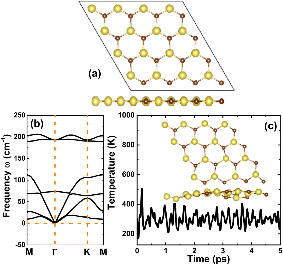 | ||
| Fig. 1 (a) A supercell of 4 × 4 × 1 size (Na atom: yellow ball; Br atom: maroon ball), (b) phonon dispersion curve, and (c) AIMD simulations recorded at 300 K (inset: atomic structure after simulations) of the NaBr monolayer. | ||
After confirming the stability, the electronic properties of the NaBr monolayer were investigated. The band structure displayed in Fig. 2a asserts the indirect gap character of the NaBr monolayer, where the valence band maximum is located at the K point and the conduction band minimum takes place at the Γ point. The PBE functional yields an energy gap of 4.52 eV, suggesting the insulator nature of the NaBr monolayer. It is well known that a material's band gap is normally underestimated by the standard GGA functional, which can be overcome by using the hybrid functional with a certain portion of the exact Hartree–Fock exchange potential. Herein, the electronic band structure of the NaBr monolayer is also calculated using the HSE06 functional.61 From Fig. 2a, the band structure profiles calculated by both functionals are quite similar, and the difference is found in the width of the forbidden energy region. Specifically, a band gap of 5.66 eV is obtained by the HSE06 functional, which is larger than that of the PBE functional as expected. The projected density of states (PDOS) spectra given in Fig. 2b show that the upper part of the valence band is formed mainly by the dense Br-pz state, while the sparse Na-s state constructs mainly the lower part of the conduction band. This feature suggests the full occupancy of the Br-pz state as well the empty Na-s state, which is a result of the charge transfer from the Na-3s orbital to the Br-4p orbital following the rule of electronegativity. This process is also confirmed by the valence charge distribution in Fig. 2c and electron localization function in Fig. 2d, where the charge accumulation is observed mainly at the Br site. Further Bader charge analysis asserts that the Br atom gains a charge quantity of 0.82 e from the Na atom. Undoubtedly, the Na–Br chemical bond is predominantly ionic, a character that is generated by charge movement.
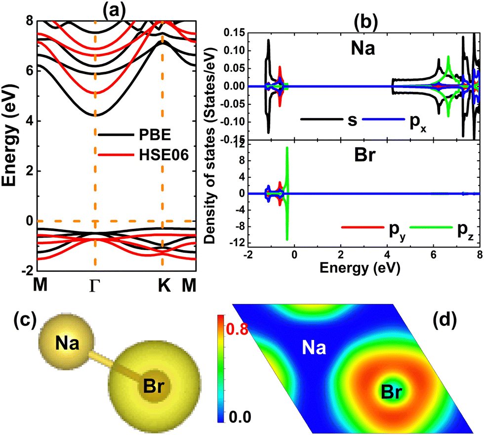 | ||
| Fig. 2 (a) Electronic band structure (the Fermi level is set to 0 eV), (b) projected density of states, (c) valence charge distribution (iso-surface value: 0.04 e Å−3), and (d) electron localization function of the NaBr monolayer. | ||
Before considering the effects of doping at the Na sublattice, a single Na vacancy is examined. Our calculations yield a formation energy of 4.38 eV that should be supplied to create a single Na vacancy in the NaBr monolayer. Moreover, a negative cohesive value of −2.64 eV per atom suggests good structural stability of the vacancy-defected system. In comparison with that of the perfect monolayer (−2.72 eV per atom), this value is slightly less negative, indicating a slight reduction of the structural stability under a single cation vacancy. A significant magnetization of the NaBr monolayer is found upon creating a single Na vacancy, which is reflected in a total magnetic moment of 1.00 μB obtained from the spin-polarized calculations. This result is derived from the deficiency of one valence electron, which is a consequence of the absence of one Na charge donor that transfers theoretically one electron to the Br atom. The illustration of the spin density in Fig. 3a implies a key role of the Br atoms closest to the vacancy site on producing magnetic properties since the unbalanced charge distribution in two spin channels is observed mainly at their locations.
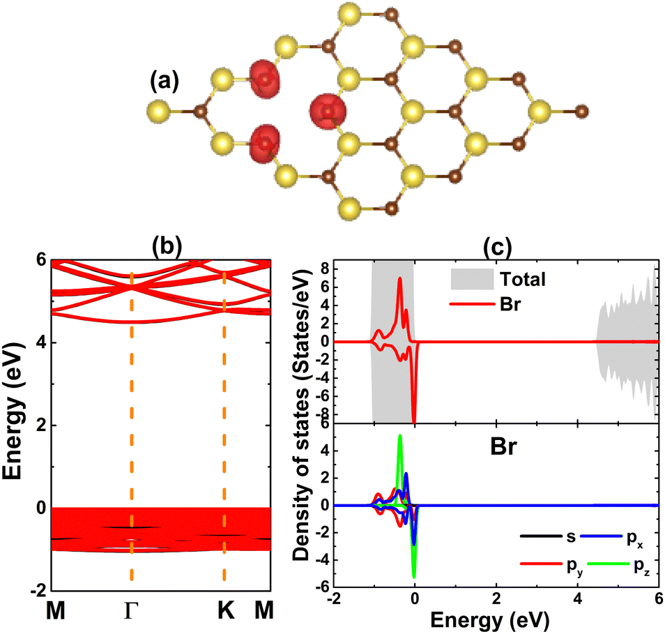 | ||
| Fig. 3 (a) Spin density (iso-value surface: 0.002 e Å−3), (b) spin-polarized band structure (the Fermi level is set to 0 eV), and (c) total density of state and projected density of state of the magnetizing Br atom of the NaBr monolayer with a single Na vacancy. | ||
The induced magnetism is also confirmed by the spin-polarized band structure and total density of states, which are displayed in Fig. 3b and c. Note that the spin polarization takes place mainly at the valence band; meanwhile, the conduction band is quite spin-symmetric. In this case, both spin states preserve their original semiconductor nature with energy gaps of 4.60 eV of the spin-up state and 4.52 eV of the spin-down state. Such that the magnetic semiconductor nature is obtained, suggesting a single Na vacancy as an effective approach to make spintronic 2D materials from a non-magnetic NaBr monolayer.62 To get more understanding on the contribution of magnetizing Br atoms, their total and projected density of states are also given. Note that in the considered energy range, these atoms only contribute to the formation of the valence band, exhibiting significant spin polarization of the p orbital. Consequently, their px, py, and pz states originate mainly the magnetism of the defected system.
B. Effects of doping with transition metals
In this part, the effects of doping with transition metals on the NaBr monolayer electronic and magnetic properties are investigated. Applying eqn (1), doping energy Ed values of 3.18, 0.49, 2.55, and 3.05 eV are obtained for V, Cr, Mn, and Fe doping, respectively. Note that V doping requires supplying the largest additional energy; meanwhile, Cr doping is thermodynamically most favorable due to its lowest Ed value. This result can be attributed to the stability of the 3d orbital when interacting with the host monolayer. Specifically, this orbital is half-filled for Cr impurities after transferring one e to the host monolayer (valence configuration from 3d54s1 to 3d5). Moreover, the obtained cohesive energy Ec values of the V-, Cr-, Mn-, and Fe-doped NaBr monolayer are −2.71, −2.70, −2.67, and −2.72 eV per atom, respectively. These values are quite similar to that of the pristine monolayer (−2.72 eV per atom), suggesting good stability of the NaBr monolayer upon doping with transition metals. Our calculations demonstrate a doping-induced high magnetization of the NaBr monolayer, reflecting large total magnetic moments. Specifically, values of 4.00, 5.00, 4.00, and 3.66 μB are obtained by doping with V, Cr, Mn, and Fe atoms, respectively. Further investigating the origin of magnetism, the spin density is illustrated in Fig. 4. Note that spin surfaces are centered mainly at transition metal impurities, indicating their key role in determining the magnetic properties of the doped systems.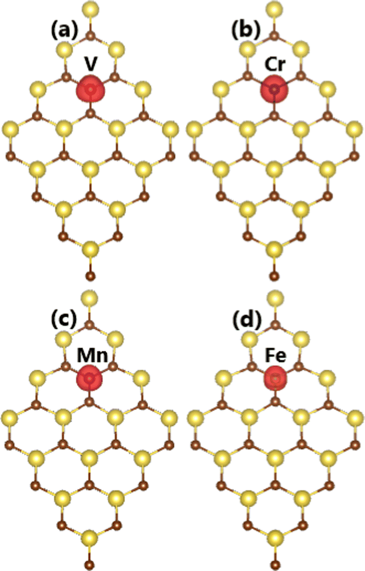 | ||
| Fig. 4 Spin density (iso-value surface: 0.01 e Å−3) in (a) V-, (b) Cr-, (c) Mn-, and (d) Fe-doped NaBr monolayer. | ||
Fig. 5 shows the spin-polarized band structures of the NaBr monolayer doped with transition metals. From the figures, one can see new flat energy branches in the forbidden energy of the NaBr monolayer (also known as middle-gap branches), which consequently determine the ground state electronic nature of the doped systems. Specifically, the V- and Fe-doped NaBr monolayers are half-metallic 2D materials considering their metallic spin-up state with electronic states crossing the Fermi level and semiconductor spin-down state. In these cases, the spin-down energy gaps are 4.49 and 3.51 eV, respectively. Unexpectedly, magnetic semiconductor behavior is obtained by doping with Cr and Mn, where new middle-gap states lead to different spin-dependent energy gaps: the spin-up band gap of Cr- and Mn-doped NaBr monolayer is 1.95 and 3.71 eV, respectively, while the spin-down state exhibits values of 4.50 and 0.35 eV, respectively (see the values summarized in Table 1). Remembering that spin current can be generated using half-metallic and magnetic semiconductor materials,62,63 doping the NaBr monolayer with transition metals can be recommended to develop new prospective 2D spintronic materials.
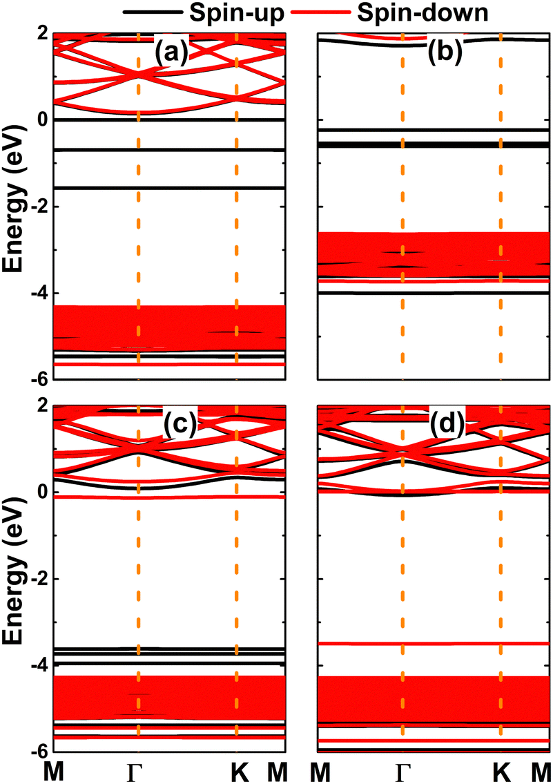 | ||
| Fig. 5 Spin-polarized band structure (the Fermi level is set to 0 eV) of (a) V-, (b) Cr-, (c) Mn-, and (d) Fe-doped NaBr monolayer. | ||
| E d | E c | E g | ΔQ | M t | |
|---|---|---|---|---|---|
| V-Doped | 3.18 | −2.71 | M/4.49 | 0.76 | 4.00 |
| Cr-Doped | 0.49 | −2.70 | 1.95/4.50 | 0.69 | 5.00 |
| Mn-Doped | 2.55 | −2.67 | 3.71/0.35 | 0.71 | 4.00 |
| Fe-Doped | 3.02 | −2.72 | M/3.51 | 0.75 | 3.66 |
| Be-Doped | 3.87 | −2.68 | M/M | 1.58 | 0.00 |
| Mg-Doped | 2.17 | −2.67 | 0.84/4.23 | 1.21 | 1.00 |
| Ca-Doped | 0.92 | −2.72 | 0.50/4.43 | 1.10 | 1.00 |
| Sr-Doped | 0.71 | −2.72 | 0.56/4.39 | 1.10 | 1.00 |
To get more insights into the interactions between the transition metal dopants and host monolayer, Bader charge analysis was carried out. The results indicate that V, Cr, Mn, and Fe impurities lose charge, transferring amounts of 0.76, 0.69, 0.71, and 0.75 e to the host monolayer, respectively. Note that these magnitudes are smaller than that from the Na atom in the host monolayer, which are a result of the larger electronegativity of the transition metals as compared to a Na atom.64,65 After transferring charge, 3d is the outermost orbital of transition metals that is partially occupied, such that they determine mainly the electronic and magnetic properties of the doped systems. This feature is confirmed through the projected density of states of impurities given in Fig. 6. As expected, the middle-gap states are formed mainly by the d orbital, where all five electronic states exhibit their important presence in the considered energy range with a strong spin polarization to induce the magnetization.
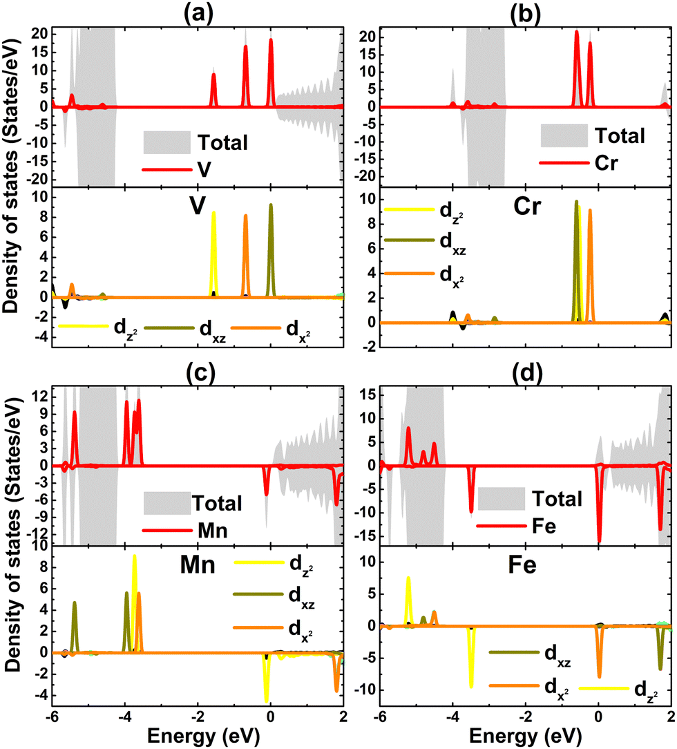 | ||
| Fig. 6 Total density of state and projected density of state of magnetic impurities of (a) V-, (b) Cr-, (c) Mn-, and (d) Fe-doped NaBr monolayer. | ||
C. Effects of doping with earth alkaline metals
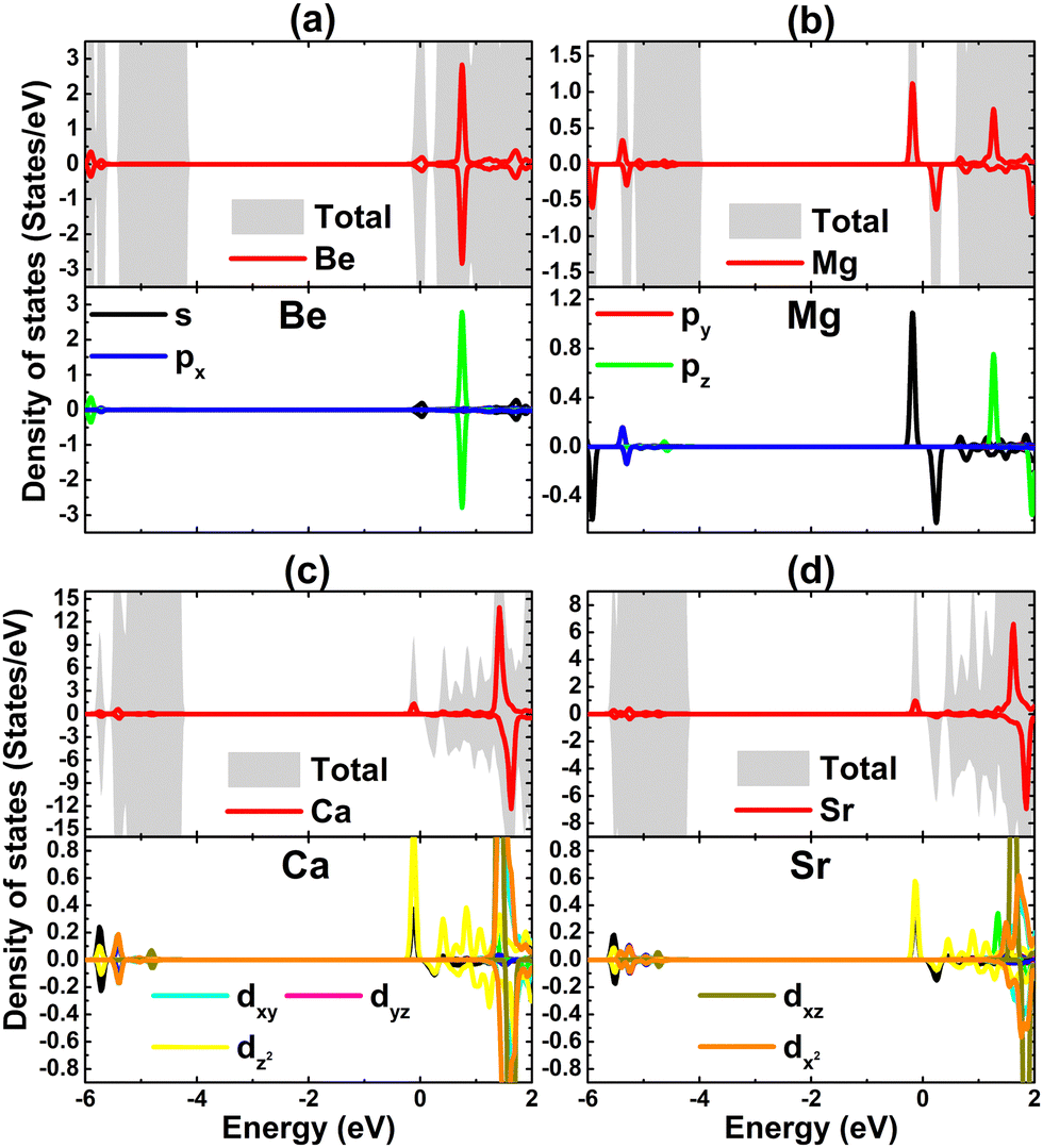
Now, the electronic and magnetic properties of the NaBr monolayer upon doping with earth alkaline metals are explored. Firstly, the doping energy and cohesive energy are calculated to examine the doping process as well as structural stability of the doped systems. According to our calculations, the Ed values for Be, Mg, Ca, and Sr dopants are 3.87, 2.17, 0.92, and 0.71 eV, respectively. These results suggest that the doping becomes easier in order to increase the atomic number of IIA-group impurities since the doping energy decreases in this direction. In other words, less additional energy is needed to realize the doping process. Large doping energies for Be and Mg are derived from their large difference in atomic size in comparison with that of the host Na atom; meanwhile, the difference is smaller for Ca and Sr atoms.66 Compared to those of transition metals (with the exception of Cr), one can see that doping with earth alkaline metals requires smaller energy. Once formed, the Be-, Mg-, Ca-, and Sr-doped systems exhibit good structural-chemical stability as suggested by negative Ec values of −2.68, −2.67, −2.72, and −2.72 eV per atom, respectively. These values are quite comparable with that of the pristine monolayer, indicating that the structural stability of the NaBr monolayer is negligibly altered by doping. It is found that the non-magnetic nature of the NaBr monolayer is preserved upon doping with Be atom, which is confirmed by the zero total magnetic moment and non spin surface in Fig. 7a. In contrast, the monolayer is significantly magnetized by doping with Mg, Ca, and Sr atoms as demonstrated by the total magnetic moment of 1.00 μB. Herein, the magnetization is derived mainly from impurities as asserted by the spin density illustration in Fig. 7c and d, where spin surfaces are centered mainly at their sites.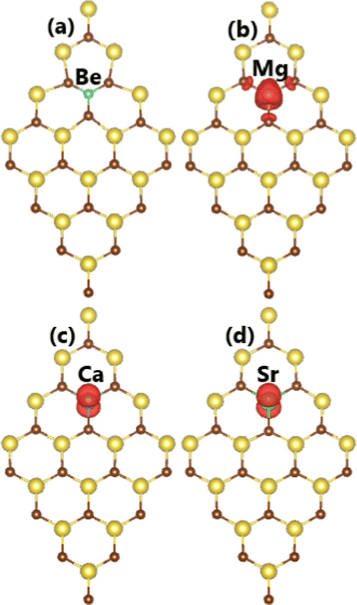 | ||
| Fig. 7 Spin density (iso-value surface: 0.002 e Å−3) in (a) Be-, (b) Mg-, (c) Ca-, and (d) Sr-doped NaBr monolayer. | ||
The calculated band structures are displayed in Fig. 8. Note that the Be-doped NaBr monolayer exhibits no spin-polarized feature, corresponding to its no magnetic nature. In this case, the monolayer is metallized due to the appearance of new middle-gap states. In contrast, the spin polarization is observed clearly in the remaining cases, mostly at the vicinity of the Fermi level and conduction band. New middle-gap states can be observed clearly around the Fermi level, which leads to the induction of the magnetic semiconductor to functionalize the NaBr monolayer for spintronic applications. The spin-dependent energy gaps are listed in Table 1. Note that the spin-up values are considerably smaller than the spin-down counterparts, which is a result of the spin-up middle-gap states below the Fermi level; meanwhile the spin-down state emerges above the Fermi level and is located away from the valence band.
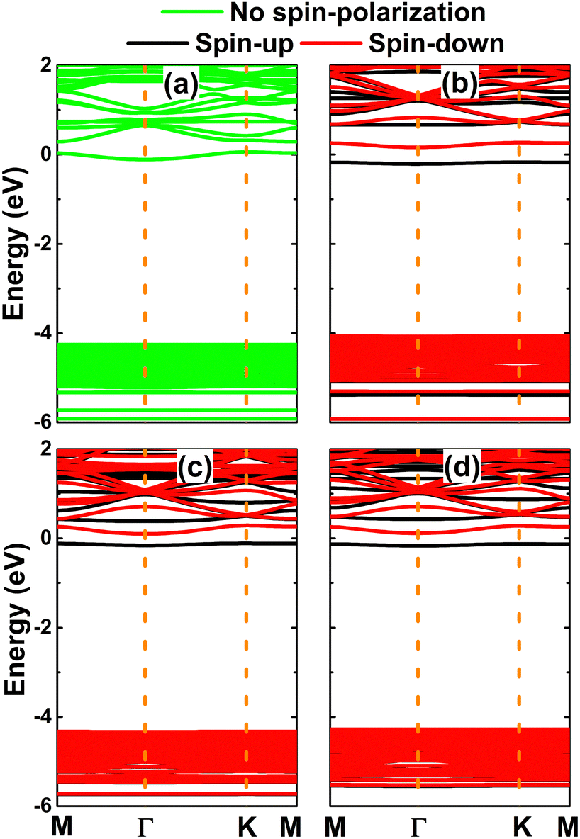 | ||
| Fig. 8 Spin-polarized band structure (the Fermi level is set to 0 eV) of (a) Be-, (b) Mg-, (c) Ca-, and (d) Sr-doped NaBr monolayer. | ||
Due to their less electronegative nature in comparison with the neighbor Br atoms, it can be expected that earth alkaline metals act as charge losers in the doped systems. This feature is further confirmed by the Bader charge analysis. Specifically, Be, Mg, Ca, and Sr impurities transfer charge quantities of 1.58, 1.21, 1.10, and 1.10 e to the host monolayer, respectively. Remembering that earth alkaline metals have two valence electrons (ns2), the charge transferred from these impurities is larger than that from the Na atom (with one valence electron: 3s1). In addition, the projected density of states of magnetizing impurities of the doped systems is displayed in Fig. 9 to investigate their contribution. Note that the metallic nature of the Be-doped NaBr monolayer is originated from the Be-s state that spreads over the Fermi level. Meanwhile, the unoccupied pz state is submerged into the conduction band. Similarly, s and pz states regulate the ground state properties of the Mg-doped systems due to their important presence around the Fermi level. Herein, the former originates flat energy branches around the Fermi level, producing magnetic semiconductor behavior. In contrast, Ca-3d and Sr-4d orbitals play a key role in the Ca- and Sr-doped systems, where the dz2 state builds mainly the band structure in the vicinity of the Fermi level that is responsible for the magnetic semiconducting. From the analyzed density of state, it can be concluded that the magnetism is originated mainly from Mg-3s, Ca-3d, and Sr-4d orbitals.
 | ||
| Fig. 9 Total density of state and projected density of state of impurities of (a) Be-, (b) Mg-, (c) Ca-, and (d) Sr-doped NaBr monolayer. | ||
IV. Conclusions
In conclusion, the electronic and magnetic properties of pristine and doped NaBr monolayers have been systematically investigated using a first-principles study. In order to induce magnetism, transition metals (V, Cr, Mn, and Fe) and earth alkaline metals (Be, Mg, Ca, Sr) have been selected as dopants. The pristine monolayer is dynamically stable without any imaginary phonon frequency, while AIMD simulations imply its thermal stability without any bond breaking after 5 ps. Besides, our calculations show the ionic character of the NaBr monolayer, which is generated by the charge transfer from the Na-s orbital to the Br-p orbital. Except for Be impurities, the monolayer is magnetized by a single Na vacancy and doping. In the first case, magnetic properties are produced mainly by the partially occupied p orbital of the Br atoms closest to the vacancy site, which is a consequence of the absence of one charge loser atom. The 3d orbital of the transition metals and Ca atom, 3s orbital of the Mg atom, and 4d orbital of the Sr atom originate new middle-gap electronic states around the Fermi level with a strong spin polarization. Consequently, they regulate mainly the electronic and magnetic properties of the doped systems. Half metallicity has been found for the V- and Fe-doped systems, while the magnetic semiconducting nature is induced in the remaining cases. These feature-rich magnetic electronic properties may recommend the creation of a single Na vacancy as well as doping with transition metals and earth alkaline metals as solid and effective ways to make new 2D spintronic materials from a non magnetic NaBr monolayer.Conflicts of interest
The authors declare that they have no known competing financial interests or personal relationships that could have appeared to influence the work reported in this paper.Acknowledgements
Calculations were performed in the DGCTIC-UNAM Supercomputing Center (projects LANCAD-UNAM-DGTIC-368) and the High-Performance Computing Systems of Thu Dau Mot University. D. M. Hoat expresses his gratitude to all the valuable support from Duy Tan University, who is going to celebrate its 30th anniversary of establishment (Nov. 11, 1994–Nov. 11, 2024) towards “Integral, Sustainable and Stable Development”.References
- K. S. Novoselov, A. K. Geim, S. V. Morozov, D.-E. Jiang, Y. Zhang, S. V. Dubonos, I. V. Grigorieva and A. A. Firsov, Electric field effect in atomically thin carbon films, Science, 2004, 306(5696), 666–669 CrossRef CAS PubMed.
- D. Akinwande, C. J. Brennan, J. S. Bunch, P. Egberts, J. R. Felts, H. Gao, R. Huang, J.-S. Kim, T. Li and Y. Li, et al., A review on mechanics and mechanical properties of 2D materialsÔÇögraphene and beyond, Extreme Mech. Lett., 2017, 13, 42–77 CrossRef.
- Q. Ma, G. Ren, K. Xu and J. Z. Ou, Tunable optical properties of 2D materials and their applications, Adv. Opt. Mater., 2021, 9(2), 2001313 CrossRef CAS.
- A. Gupta, T. Sakthivel and S. Seal, Recent development in 2D materials beyond graphene, Prog. Mater. Sci., 2015, 73, 44–126 CrossRef CAS.
- S. Kang, D. Lee, J. Kim, A. Capasso, H. S. Kang, J.-W. Park, C.-H. Lee and G.-H. Lee, 2D semiconducting materials for electronic and optoelectronic applications: potential and challenge, 2D Mater., 2020, 7(2), 022003 CrossRef CAS.
- J. Shim, H.-Y. Park, D.-H. Kang, J.-O. Kim, S.-H. Jo, Y. Park and J.-H. Park, Electronic and optoelectronic devices based on two-dimensional materials: From fabrication to application, Adv. Electron. Mater., 2017, 3(4), 1600364 CrossRef.
- W. Liu, M. Liu, X. Liu, X. Wang, H.-X. Deng, M. Lei, Z. Wei and Z. Wei, Recent advances of 2D materials in nonlinear photonics and fiber lasers, Adv. Opt. Mater., 2020, 8(8), 1901631 CrossRef CAS.
- Y. Fang, Y. Ge, C. Wang and H. Zhang, Mid-infrared photonics using 2D materials: status and challenges, Laser Photonics Rev., 2020, 14(1), 1900098 CrossRef CAS.
- P. Zhang, F. Wang, M. Yu, X. Zhuang and X. Feng, Two-dimensional materials for miniaturized energy storage devices: from individual devices to smart integrated systems, Chem. Soc. Rev., 2018, 47(19), 7426–7451 RSC.
- T.-H. Le, Y. Oh, H. Kim and H. Yoon, Exfoliation of 2D materials for energy and environmental applications, Chem. – Eur. J., 2020, 26(29), 6360–6401 CrossRef CAS PubMed.
- F. R. Fan, R. Wang, H. Zhang and W. Wu, Emerging beyond-graphene elemental 2D materials for energy and catalysis applications, Chem. Soc. Rev., 2021, 50(19), 10983–11031 RSC.
- J. Zhu, E. Ha, G. Zhao, Y. Zhou, D. Huang, G. Yue, L. Hu, N. Sun, Y. Wang and L. Y. S. Lee, et al., Recent advance in MXenes: a promising 2D material for catalysis, sensor and chemical adsorption, Coord. Chem. Rev., 2017, 352, 306–327 CrossRef CAS.
- E. C. Ahn, 2D materials for spintronic devices, npj 2D Mater. Appl., 2020, 4(1), 17 CrossRef CAS.
- Y. P. Feng, L. Shen, M. Yang, A. Wang, M. Zeng, Q. Wu, S. Chintalapati and C.-R. Chang, Prospects of spintronics based on 2D materials, Wiley Interdiscip. Rev.: Comput. Mol. Sci., 2017, 7(5), e1313 Search PubMed.
- L. Tao, E. Cinquanta, D. Chiappe, C. Grazianetti, M. Fanciulli, M. Dubey, A. Molle and D. Akinwande, Silicene field-effect transistors operating at room temperature, Nat. Nanotechnol., 2015, 10(3), 227–231 CrossRef CAS PubMed.
- M. E. Dávila and G. Le Lay, Few layer epitaxial germanene: a novel two-dimensional Dirac material, Sci. Rep., 2016, 6(1), 20714 CrossRef PubMed.
- J.-K. Lyu, S.-F. Zhang, C.-W. Zhang and P.-J. Wang, Stanene: a promising material for new electronic and spintronic applications, Ann. Phys., 2019, 531(10), 1900017 CrossRef CAS.
- C. Polley, H. Fedderwitz, T. Balasubramanian, A. Zakharov, R. Yakimova, O. Bäcke, J. Ekman, S. Dash, S. Kubatkin and S. Lara-Avila, Bottom-up growth of monolayer honeycomb SiC, Phys. Rev. Lett., 2023, 130(7), 076203 CrossRef CAS PubMed.
- L. Li, Y. Yu, G. J. Ye, Q. Ge, X. Ou, H. Wu, D. Feng, X. H. Chen and Y. Zhang, Black phosphorus field-effect transistors, Nat. Nanotechnol., 2014, 9(5), 372–377 CrossRef CAS PubMed.
- T. Hong, B. Chamlagain, W. Lin, H.-J. Chuang, M. Pan, Z. Zhou and Y.-Q. Xu, Polarized photocurrent response in black phosphorus field-effect transistors, Nanoscale, 2014, 6(15), 8978–8983 RSC.
- J. Shah, W. Wang, H. M. Sohail and R. Uhrberg, Experimental evidence of monolayer arsenene: an exotic 2D semiconducting material, 2D Mater., 2020, 7(2), 025013 CrossRef CAS.
- Y. Stehle, H. M. Meyer III, R. R. Unocic, M. Kidder, G. Polizos, P. G. Datskos, R. Jackson, S. N. Smirnov and I. V. Vlassiouk, Synthesis of hexagonal boron nitride monolayer: control of nucleation and crystal morphology, Chem. Mater., 2015, 27(23), 8041–8047 CrossRef CAS.
- K. K. Kim, A. Hsu, X. Jia, S. M. Kim, Y. Shi, M. Hofmann, D. Nezich, J. F. Rodriguez-Nieva, M. Dresselhaus and T. Palacios, et al., Synthesis of monolayer hexagonal boron nitride on Cu foil using chemical vapor deposition, Nano Lett., 2012, 12(1), 161–166 CrossRef PubMed.
- J. Gusakova, X. Wang, L. L. Shiau, A. Krivosheeva, V. Shaposhnikov, V. Borisenko, V. Gusakov and B. K. Tay, Electronic properties of bulk and monolayer TMDs: theoretical study within DFT framework (GVJ-2e method), Phys. Status Solidi A, 2017, 214(12), 1700218 CrossRef.
- S.-H. Su, W.-T. Hsu, C.-L. Hsu, C.-H. Chen, M.-H. Chiu, Y.-C. Lin, W.-H. Chang, K. Suenaga, J.-H. He and L.-J. Li, Controllable synthesis of band-gap-tunable and monolayer transition-metal dichalcogenide alloys, Front. Energy Res., 2014, 2, 27 Search PubMed.
- Y. Shi, H. Li and L.-J. Li, Recent advances in controlled synthesis of two-dimensional transition metal dichalcogenides via vapour deposition techniques, Chem. Soc. Rev., 2015, 44(9), 2744–2756 RSC.
- E. S. Penev, N. Marzari and B. I. Yakobson, Theoretical prediction of two-dimensional materials, behavior, and properties, ACS Nano, 2021, 15(4), 5959–5976 CrossRef CAS PubMed.
- M. Ashton, N. Trometer, K. Mathew, J. Suntivich, C. Freysoldt, S. B. Sinnott and R. G. Hennig, Predicting the electrochemical synthesis of 2D materials from first principles, J. Phys. Chem. C, 2019, 123(5), 3180–3187 CrossRef CAS.
- H. Zheng, X.-B. Li, N.-K. Chen, S.-Y. Xie, W. Q. Tian, Y. Chen, H. Xia, S. Zhang and H.-B. Sun, Monolayer II-VI semiconductors: A first-principles prediction, Phys. Rev. B: Condens. Matter Mater. Phys., 2015, 92(11), 115307 CrossRef.
- P. Devi, D. Mahendiran and P. Murugan, First principles study on thickness dependent structural and electronic properties unveiling the growth and stability of 2D layered II-VI semiconducting compounds, Phys. Chem. Chem. Phys., 2022, 24(39), 24296–24305 RSC.
- T. Suzuki, Theoretical discovery of stable structures of group III-V monolayers: The materials for semiconductor devices, Appl. Phys. Lett., 2015, 107, 213105 CrossRef.
- H. Sahin, S. Cahangirov, M. Topsakal, E. Bekaroglu, E. Akturk, R. T. Senger and S. Ciraci, Monolayer honeycomb structures of group-IV elements and III-V binary compounds: First-principles calculations, Phys. Rev. B: Condens. Matter Mater. Phys., 2009, 80(15), 155453 CrossRef.
- T.-Y. Lü, X.-X. Liao, H.-Q. Wang and J.-C. Zheng, Tuning the indirect-direct band gap transition of SiC, GeC and SnC monolayer in a graphene-like honeycomb structure by strain engineering: a quasiparticle GW study, J. Mater. Chem., 2012, 22(19), 10062–10068 RSC.
- P. Li, W. Wu, Y. Xu, J. Liu, S. Wu, Y. Ye, C. Liang and X. C. Zeng, Two-dimensional IV-V monolayers with highly anisotropic carrier mobility and electric transport properties, J. Phys. Chem. Lett., 2021, 12(3), 1058–1065 CrossRef CAS PubMed.
- W. Zhang, J. Yin, Y. Ding, Y. Jiang and P. Zhang, Strain-engineering tunable electron mobility of monolayer IV-V group compounds, Nanoscale, 2018, 10(35), 16750–16758 RSC.
- M. Pumera and Z. Sofer, 2d monoelemental arsenene, antimonene, and bismuthene: beyond black phosphorus, Adv. Mater., 2017, 29(21), 1605299 CrossRef PubMed.
- F. Ersan, D. Keçik, V. Özçelik, Y. Kadioglu, O. Ü. Aktürk, E. Durgun, E. Aktürk and S. Ciraci, Two-dimensional pnictogens: A review of recent progresses and future research directions, Appl. Phys. Rev., 2019, 6, 021308 Search PubMed.
- M. Prencipe, A. Zupan, R. Dovesi, E. Apra and V. Saunders, Ab initio study of the structural properties of LiF, NaF, KF, LiCl, NaCl, and KCl, Phys. Rev. B: Condens. Matter Mater. Phys., 1995, 51(6), 3391 CrossRef CAS PubMed.
- J. Wang, M. Deng, Y. Chen, X. Liu, W. Ke, D. Li, W. Dai and K. He, Structural, elastic, electronic and optical properties of lithium halides (LiF, LiCl, LiBr, and LiI): First-principle calculations, Mater. Chem. Phys., 2020, 244, 122733 CrossRef CAS.
- D. Hoat, M. Naseri, N. T. Binh, J. Rivas-Silva, T. V. Vu and G. H. Cocoletzi, LiCl monolayer for UV detection: First principles prediction, Phys. E, 2020, 123, 114168 CrossRef CAS.
- B. Luo, Y. Yao, E. Tian, H. Song, X. Wang, G. Li, K. Xi, B. Li, H. Song and L. Li, Graphene-like monolayer monoxides and monochlorides, Proc. Natl. Acad. Sci. U. S. A., 2019, 116(35), 17213–17218 CrossRef CAS PubMed.
- M.-Y. Ma, N.-K. Chen, D. Wang, D. Han, H.-B. Sun, S. Zhang and X.-B. Li, Defect physics in 2D monolayer I-VII semiconductor AgI, Mater. Today Nano, 2023, 22, 100304 CrossRef CAS.
- M. B. Kanoun, Tuning magnetic properties of two-dimensional MoTe2 monolayer by doping 3d transition metals: Insights from first principles calculations, J. Alloys Compd., 2018, 748, 938–942 CrossRef CAS.
- X. Fan, J. Jiang, R. Li and W. Mi, Half-metallicity and magnetic anisotropy in transition-metal-atom-doped graphitic germanium carbide (g-GeC) monolayers, J. Phys. Chem. C, 2021, 125(24), 13688–13695 CrossRef CAS.
- P. Wu and M. Huang, Transition metal doped arsenene: Promising materials for gas sensing, catalysis and spintronics, Appl. Surf. Sci., 2020, 506, 144660 CrossRef CAS.
- A. Hirohata and K. Takanashi, Future perspectives for spintronic devices, J. Phys. D: Appl. Phys., 2014, 47(19), 193001 CrossRef.
- A. Hirohata, K. Yamada, Y. Nakatani, I.-L. Prejbeanu, B. Diény, P. Pirro and B. Hillebrands, Review on spintronics: Principles and device applications, J. Magn. Magn. Mater., 2020, 509, 166711 CrossRef CAS.
- I. Choudhuri, P. Bhauriyal and B. Pathak, Recent advances in graphene-like 2D materials for spintronics applications, Chem. Mater., 2019, 31(20), 8260–8285 CrossRef CAS.
- W. Han, Perspectives for spintronics in 2D materials, APL Mater., 2016, 4(3), 032401 CrossRef.
- R.-Z. Zhang, X.-H. Cui, H.-L. Cui and X.-H. Li, First-principles study of structural, electronic and magnetic properties of transition metal doped Sc2 CF2 MXene, Appl. Surf. Sci., 2022, 581, 152360 CrossRef CAS.
- P. V. Gaikwad, Transition metal doping engineered octagonal ZnO monolayer magnetic properties, Mater. Res. Express, 2019, 6(5), 056106 CrossRef CAS.
- G. Kresse and J. Furthmüller, Efficiency of ab-initio total energy calculations for metals and semiconductors using a plane-wave basis set, Comput. Mater. Sci., 1996, 6(1), 15–50 CrossRef CAS.
- G. Kresse and J. Furthmüller, Efficient iterative schemes for ab initio total-energy calculations using a plane-wave basis set, Phys. Rev. B: Condens. Matter Mater. Phys., 1996, 54(16), 11169 CrossRef CAS PubMed.
- W. Kohn and L. J. Sham, Self-consistent equations including exchange and correlation effects, Phys. Rev., 1965, 140(4A), A1133 CrossRef.
- J. P. Perdew, K. Burke and M. Ernzerhof, Generalized gradient approximation made simple, Phys. Rev. Lett., 1996, 77(18), 3865 CrossRef CAS PubMed.
- S. L. Dudarev, G. A. Botton, S. Y. Savrasov, C. Humphreys and A. P. Sutton, Electron-energy-loss spectra and the structural stability of nickel oxide: An LSDA + U study, Phys. Rev. B: Condens. Matter Mater. Phys., 1998, 57(3), 1505 CrossRef CAS.
- Y. Wang, S. Li and J. Yi, Transition metal-doped tin monoxide monolayer: a first-principles study, J. Phys. Chem. C, 2018, 122(8), 4651–4661 CrossRef CAS.
- H. J. Monkhorst and J. D. Pack, Special points for Brillouin-zone integrations, Phys. Rev. B: Solid State, 1976, 13(12), 5188 CrossRef.
- R. C. Andrew, R. E. Mapasha, A. M. Ukpong and N. Chetty, Mechanical properties of graphene and boronitrene, Phys. Rev. B: Condens. Matter Mater. Phys., 2012, 85(12), 125428 CrossRef.
- S. Thomas, K. Ajith and M. Valsakumar, Directional anisotropy, finite size effect and elastic properties of hexagonal boron nitride, J. Phys.: Condens. Matter, 2016, 28(29), 295302 CrossRef PubMed.
- A. V. Krukau, O. A. Vydrov, A. F. Izmaylov and G. E. Scuseria, Influence of the exchange screening parameter on the performance of screened hybrid functionals, J. Chem. Phys., 2006, 125(22), 224106 CrossRef PubMed.
- X. Li and J. Yang, First-principles design of spintronics materials, Natl. Sci. Rev., 2016, 3(3), 365–381 CrossRef CAS.
- X. Li and X. Wu, Two-dimensional monolayer designs for spintronics applications, Wiley Interdiscip. Rev.: Comput. Mol. Sci., 2016, 6(4), 441–455 CAS.
- R. T. Sanderson, Electronegativity and bond energy, J. Am. Chem. Soc., 1983, 105(8), 2259–2261 CrossRef CAS.
- J. B. Mann, T. L. Meek, E. T. Knight, J. F. Capitani and L. C. Allen, Configuration energies of the d-block elements, J. Am. Chem. Soc., 2000, 122(21), 5132–5137 CrossRef CAS.
- J. C. Slater, Atomic radii in crystals, J. Chem. Phys., 1964, 41(10), 3199–3204 CrossRef CAS.
| This journal is © The Royal Society of Chemistry 2024 |