
 Open Access Article
 This Open Access Article is licensed under a Creative Commons Attribution-Non Commercial 3.0 Unported Licence
Optical and chemical properties of As–Se and As–S–Se solution processed thin films prepared via As50Se50 source solution modification†
Jiri
Jemelka
a,
Michal
Kurka
b,
Stanislav
Slang
 b,
Jiri
Jancalek
b,
Karel
Palka
*ab and
Miroslav
Vlcek
ab
b,
Jiri
Jancalek
b,
Karel
Palka
*ab and
Miroslav
Vlcek
ab
aDepartment of General and Inorganic Chemistry, Faculty of Chemical Technology, University of Pardubice, Studentska 95, 53210 Pardubice, Czech Republic. E-mail: karel.palka@upce.cz
bCenter of Materials and Nanotechnologies, Faculty of Chemical Technology, University of Pardubice, Studentska 95, 53210 Pardubice, Czech Republic
First published on 2nd January 2024
Abstract
This work presents the prospect of As–S–Se and As–Se thin film preparation from a modified solution of As50Se50 chalcogenide glass in ethylenediamine. The source solution was modified by direct dissolution of elemental sulfur and amorphous elemental selenium. Using this method, we successfully prepared four sulfur-modified (As45S10Se45, As40S20Se40, As35S30Se35, and As30S40Se30) and four selenium-modified (As45Se55, As40Se60, As35Se65, and As30Se70) solutions. Thin films of all compositions (including unmodified As50Se50) were deposited in specular optical quality using spin coating. The structure, composition, organic residue content, refractive index, optical band gap, surface roughness, and chemical resistance of thin films were studied depending on the annealing temperature. The obtained data suggest the incorporation of both sulfur and selenium into the glass structure already in the solution, which resulted in changes of the optical and chemical properties of thin films. According to our observation both composition and proximity to stoichiometric composition have a major impact on the optical and chemical properties of the studied thin films. The solution modification allows easy preparation of thin films with multiple different compositions from a single source solution.
Introduction
Chalcogenide glasses are amorphous materials that contain one or more chalcogens (S, Se, and Te) as their primary component and usually one or more 14th or 15th group elements as their secondary component. Compared to oxide or halide glasses, which are usually insulators with band gaps between 5 and 10 eV, chalcogenide glasses are semiconducting materials with band gap values between 1 and 3 eV.1 Chalcogenide glasses are intensively studied materials with desirable optical properties such as a high refractive index and a wide transparency window in the IR region. They have many possible applications, including elements for IR optics, optoelectronics, and photonics.1–3Chalcogenide glasses can be used either in a bulk form,4 fibres5 or as thin films on appropriate substrates.6,7 Thin films can be prepared by vacuum deposition methods, such as thermal evaporation,6 sputtering,8 and laser ablation.9 Alternatively, due to their acidic character, chalcogenide glasses can be dissolved in alkaline solvents, for example volatile amines or amine-based solvent mixtures.10–12 The solution can be used to deposit thin films by various techniques, including spin-coating,10 dip-coating,13 and spray-coating.14 Solution-based methods are generally cheaper because they do not need expensive high-vacuum equipment. The solution-based methods also enable modification of the source solution by adding new components (e.g., metal nanoparticles and quantum dots) or mixing several chalcogenide glass solutions of different compositions.15–17
In our previous work,18 we were unable to study modified As–S chalcogenide glasses with arsenic overstoichiometry, because As-rich glasses of the As–S system have high tendency for crystallization even at low overstoichiometry of As (glass forming region of 4.9 to 46.1 at% of arsenic). In this work, the glass of the As–Se system, which has a wider glass forming region (0 at% to 60 at% of arsenic), was chosen.19 The As50Se50 glass is well-known for its photoinduced phenomena in thermally deposited thin films.20 The solution-processed thin films have already been prepared from As50Se50,21 As40Se60,12,22 As33Se67,23 and As30Se7011 as well as several compositions of the As–S–Se glass system.23,24 Our work presents a comparative study of nine As–Se and As–S–Se compositions prepared from a single solvent (ethylenediamine), using the same mass concentration of a target glass composition by modifying the source solution of the As50Se50 chalcogenide glass by elemental sulfur and selenium.
The modification of As50Se50 glass solution with arsenic-overstoichiometry allows us to study the influence of compositions with the overstoichiometry of arsenic and chalcogen on the properties of modified thin films in As–Se and As–S–Se glass systems. This method allows us to produce thin films of several compositions with different optical and chemical properties, from a single bulk glass solution modified by pure elements, and compare their optical and chemical properties. The compositional range includes glasses with arsenic overstoichiometry (As50Se50, As45Se55, and As45S10Se45), stoichiometric glasses (As40Se60 and As40S20Se40), and glasses with chalcogen overstoichiometry (As35Se65, As30Se70, As35S30S35, and As30S40Se30). The stoichiometric composition corresponds to the ratio of elements in the As2X3 crystal (X = chalcogen). We studied the thickness (d), optical properties (refractive index at 1550 nm n1550![[thin space (1/6-em)]](https://www.rsc.org/images/entities/char_2009.gif) nm and optical band gap Eoptg), surface roughness (RMS), structure, and chemical resistance of deposited chalcogenide thin films depending on the annealing temperature and glass composition (including the influence of proximity to As2X3 stoichiometry).
nm and optical band gap Eoptg), surface roughness (RMS), structure, and chemical resistance of deposited chalcogenide thin films depending on the annealing temperature and glass composition (including the influence of proximity to As2X3 stoichiometry).
This work offers insight into structural changes, induced by modification of compositions, in both solutions and consequently deposited thin films of As–Se and As–S–Se chalcogenide glass systems. Structural changes in the glass matrix significantly affect the optical and chemical properties of the deposited thin films. The modification of glass solution by pure elements allows the preparation of a wide range of glass compositions from the single bulk glass. Because the bulk glass synthesis of several compositions can be time consuming, our method significantly simplifies the process. This could be beneficial for research groups without the equipment for bulk synthesis, offering them a way to study previously unavailable chalcogenide glass compositions prepared from single commercially available bulk glass such as As2S3 (AMTIR–6 and IRG 27) or As2Se3 (AMTIR-2 and IRG 26). The modification of glass solution could also be advantageous for optical element manufacturing as it allows the easy precise tuning of glass compositions and thus optical properties.
Experimental
Bulk chalcogenide glass of the As50Se50 composition was synthesized using the standard melt-quench method. Calculated amounts of high purity (5N) elements were loaded into a quartz ampoule and sealed under vacuum (10−3 Pa). The ampule was heated in a rocking tube furnace to 850 °C for 32 hours and quenched in cold water afterward.Amorphous selenium was also prepared using the melt-quench method. High-purity selenium (5N) was introduced into a quartz ampoule, heated to 500 °C in a rocking tube furnace for 24 hours, and subsequently quenched in cold water.
Bulk As50Se50 glass was then pulverized in an agate bowl and subsequently dissolved in ethylenediamine (EDA) inside a nitrogen-filled glovebox (Unilab Pro SP 1800/780, MBraun) under intensive stirring using a magnetic stirrer. After the glass was fully dissolved, calculated amounts of high purity (5N) sulfur or amorphous selenium were dissolved in the As50Se50 glass solution targeting a concentration of 0.2 g of targeted glass composition per 1 mL of solvent (the concentration of As50Se50 source solution was adjusted accordingly). The solution was agitated using a vortex mixture (mixer Classic, Velp) during dissolution. All solutions were homogenous without any precipitate or turbidity.
Chalcogenide glass solutions of four sulfur-modified (As45S10Se45, As40S20Se40, As35S30Se35, and As30S40Se30) and four selenium-modified (As45Se55, As40Se60, As35Se65, and As30Se70) compositions were prepared using this method.
Chalcogenide glass thin films were deposited by the spin-coating method. The solution of the chalcogenide glass was spin-coated (spin-coater Laurell WS-650Mz-23NPPB) on the soda-lime glass substrate under a nitrogen atmosphere for 60 s at a spin rate of 1500 rpm and subsequently annealed at 60 °C on a hot plate for 20 minutes (hereafter referred to as “as-prepared” samples). As-prepared thin films were further stabilized by annealing at 90, 120, 150 and 180 °C for 1 hour on a hot plate in a nitrogen-filled glovebox. The optical properties of thin films annealed at 180 °C were not studied due to low optical quality and/or crystallization. The temperature range was chosen based on the preliminary experiment and published values of the glass transition temperature (Tg) of glasses with similar compositions (Tg = 173 °C for As50Se50, Tg = 186 °C for As40Se60, Tg = 125 °C for As30Se70, Tg = 196 °C for As40S15Se45, Tg = 154 °C for As32S34Se34, and Tg = 135 °C for As24S38Se3819,25,26).
Transmission spectra were recorded using a UV-VIS-NIR spectrometer UV3600 (Shimadzu) in the spectral range of 190–2000 nm. Transmission spectra were recorded on three samples of each annealing temperature and thin film compositions. The thickness and refractive index of prepared thin films were determined from UV-VIS-NIR transmission spectra using the fitting procedure described in ref. 24 based on a combination of Swanepoel's model of thin films on the finite substrate27 and Wemple–DiDomenico's equation.28 The optical band gap was determined using Tauc's method for semiconductors.29 The presented thickness and optical parameter values stand for the mean value of experimental results, and standard deviations are shown as error bars. The example UV-VIS-NIR spectra of thin films are provided in the ESI† (Fig. S2).
Raman spectra were recorded using a MultiRAM (Bruker) FT-Raman spectrometer using a 1064 nm Nd:YAG excitation laser (a resolution of 2 cm−1, an average of 64 scans for thin films and 200 scans for chalcogenide glass solutions). The measured spectra of thin films were normalized by the intensity of the most intensive band and spectra of solutions by the intensity of the most intensive band in the pure EDA spectrum (475 cm−1).
The surface roughness and topography of thin films were studied using atomic force microscopy (AFM) in the semi-contact mode using a NTEGRA microscope (NT-MDT) equipped with HA_HR tips (ScanSens). Three areas of 5 × 5 μm were measured for each annealing temperature and thin film compositions. The presented values of RMS (calculated according to ISO 4287/1 norm) are the average values of three scans with error bars representing standard deviations. The AFM scans of all studied thin films are provided in the ESI† (Fig. S4).
Elemental compositions and scanning electron microscopy (SEM) scans were obtained using a scanning electron microscope LYRA 3 (Tescan) equipped with an EDX analyzer Aztec X-Max20 (Oxford Instruments). Samples were measured on five 400 × 400 μm areas at an accelerating voltage of 5 kV. The SEM scans of the studied samples are provided in the ESI† (Fig. S3).
The chemical resistance of thin films was studied by etching thin films in the solution of 5 vol% ethylenediamine in dimethyl sulfoxide at 25 °C. Etching rates were evaluated using the procedure described in ref. 30
Results and discussion
Glass stoichiometry can significantly influence chalcogenide glass properties. The stoichiometric arsenic-based chalcogenide glass or crystal possesses exact As2X3 (i.e. As40X60 in at%, where X represents the chalcogen). In the crystalline form, the material of the stoichiometric composition contains precise amounts of tri-valent arsenic and bi-valent chalcogen that each arsenic is bonded to three chalcogen atoms and each chalcogen atom to two arsenic atoms (As2X3). In the amorphous state, glass of the same composition forms a highly polymerized glass matrix, which has the same short-range order as the crystal, but the long-range order of the crystalline lattice is disrupted. The comparison of the crystalline and glass structure of the As2S3 (i.e. As40S60 in at%) composition is shown in Fig. 1. In glasses with arsenic overstoichiometry (at% (As) > 40), the glass matrix will contain an increased amount of As–As homopolar bonds, at high arsenic overstoichiometry even As-rich clusters (As4X3 and As4X4) embedded into the glass polymer structure. In contrast, in the case of chalcogen overstoichiometry (at% (X) > 60), the presence of chalcogen chains (Sn and Sen) and even chalcogen rings (S8 and Se8) can be detected. For this reason, both arsenic and chalcogen overstoichiometric glasses of As–S and As–Se systems have lower chemical resistance and lower glass transition temperature than stoichiometric ones.19,31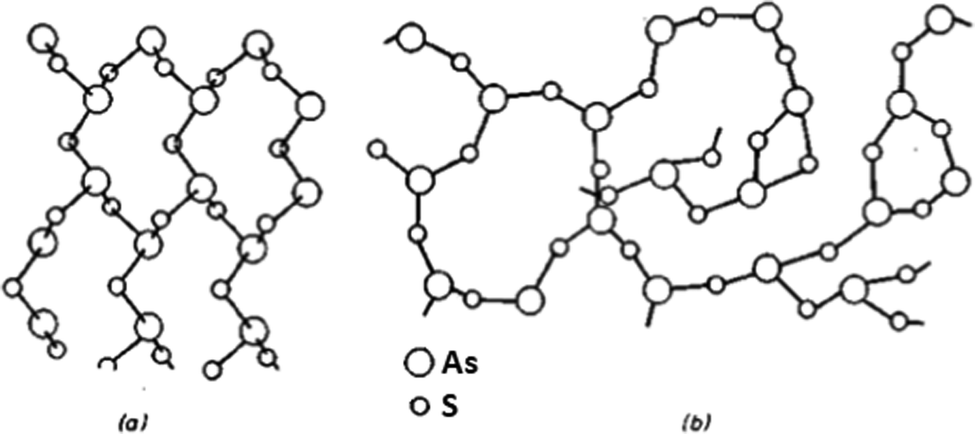 | ||
| Fig. 1 Lattice of (a) crystalline As2S3 and (b) glassy As2S3. Reprinted from ref. 32 with permission from John Wiley and Sons. | ||
The solution of the As50Se50 chalcogenide glass in ethylenediamine (EDA) was modified by dissolving elemental sulfur and selenium directly in the glass solution. Four selenium-modified (As45Se55, As40Se60, As35Se65, and As30Se70) and four sulfur-modified (As45S10Se45, As40S20Se40, As35S30Se35, and As30S40Se30) solutions were prepared. The gradual change in the solution color from dark red to bright red was observed for both sulfur and selenium-modified solutions. The photographs of As50Se50, as well as the modified chalcogenide glass solutions, are presented in Fig. 2.
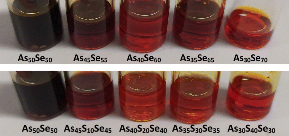 | ||
| Fig. 2 Photographs of As50Se50 and the selenium- and sulfur-modified chalcogenide glass solutions. | ||
The chemical structure of the glass solutions was investigated using Raman spectroscopy. The Raman spectra of all solutions and pure EDA solvent are shown in Fig. 3. All spectra were normalized by the most intensive band of pure EDA (475 cm−1). The identification of As–Se bands is estimated based on the positions of bands in the Raman spectra of thin films and/or bulk glass12,33,34 and changes in the intensity of Raman bands in both solutions and thin films with changing compositions. As far as we know, these bands are not yet described in any published literature. The identified Raman bands in chalcogenide glass solutions are presented in Table 1.
 | ||
| Fig. 3 Raman spectra of pure solvent and (a) selenium-modified and (b) sulfur-modified As50Se50 glass solutions. | ||
| Wavenumber (cm−1) | Vibration of | Source |
|---|---|---|
| 196 | As–As bond in As4Se4 and As4Se3 | Assumed |
| 220 | As–Se bond in As4Se3 | Assumed |
| 228 | AsSe3/2 | Assumed |
| 244 | Se-chains | 33 and 35 |
| 253 | As–Se bond in As4Se4 | Assumed |
| 267 | Se8 rings | 33 and 35 |
| 267 | As4Se3 | Assumed |
| 300 | Unknown As-based dissolution product | Assumed |
| 373 | As–S bond in As4S4 | 33 and 36 |
| 406 | Polysulfides | 37 |
| 438 | S-chains | 33 and 36 |
The source solution of the As50Se50 glass contains As4Se4 and As4Se3 clusters (253 cm−1 and 220 cm−1), accompanied by AsSe3/2 pyramids (228 cm−1), with no observable Se-chain (244 cm−1) content. The gathered data suggest that the band at 267 cm−1 probably represents some vibrations of As4Se3 clusters in As-rich samples (As50Se50, As45Se55, and As45S10Se45). The similar behavior of the bands at 220 cm−1 and 267 cm−1 in As-rich samples further supports this hypothesis. With further selenium addition, the contents of As4Se3 and As4Se4 clusters decrease, and the content of AsSe3/2 pyramids increases. This suggests a reaction between As-rich clusters and elemental selenium, forming AsSe3/2 pyramidal units. In Se-rich glasses formed by further selenium addition, this structure is present and accompanied by overstoichiometric selenium in the form of Se8 rings (267 cm−1) and Se-chains (244 cm−1).
In the sulfur-modified glass solutions, we can observe similar changes in the selenium-based structural units as in the selenium-based solutions (transition from As-rich clusters to the AsSe3/2 pyramid structure, accompanied by Se8 rings and Se-chains). Additionally, with the increasing sulfur content, As4S4 clusters (373 cm−1) are formed in the solution when sulfur replaces the selenium in the As-rich clusters due to the higher affinity of sulfur to arsenic (even in As-rich compositions).32
Due to the adjustment of solution concentrations (lower concentration of As50Se50 source solution – see the Experimental section), the concentration of As4S4 clusters in overstoichiometric glasses decreases with added sulfur. With the increasing sulfur content, the gradual formation of the S-chain (438 cm−1) is observed. The solutions with the highest sulfur content also contain polysulfides (406 cm−1) formed from overstoichiometric sulfur. Significant changes in Raman spectra of solutions indicate the incorporation of pure elements into the glass structure already in the solution state.
The exact nature of the Raman peak at 300 cm−1 is currently unknown. As far as we know, this band is not assigned in any literature and does not directly correspond to any band found in the bulk glass/thin film. The gathered data suggest that this band belongs to some kind of As–Se based dissolution product vibration (compound created as a result of the chemical reaction between the inorganic glass matrix and ethylenediamine), due to the weaker signal of this band in highly S-modified solutions. Also, the presence of this band in As30Se70 solution, where no significant bands of As structures are present, supports this theory.
The Raman spectra of all studied thin films were recorded and are presented in the ESI† (Fig. S1). In Fig. 4 and 5, we present the Raman spectra of as-prepared thin films and thin films annealed at 150 °C (the highest temperature at which all samples still possessed optical quality). The Raman spectra of 180 °C annealed samples show similar thermo-induced structural changes. The spectra were normalized by the most intensive band in the 150–550 cm−1 region. Changes in the chemical structure are strongly dependent on both the chalcogenide thin film composition and the annealing temperature. The identified Raman bands in chalcogenide glass thin films are presented in Table 2.
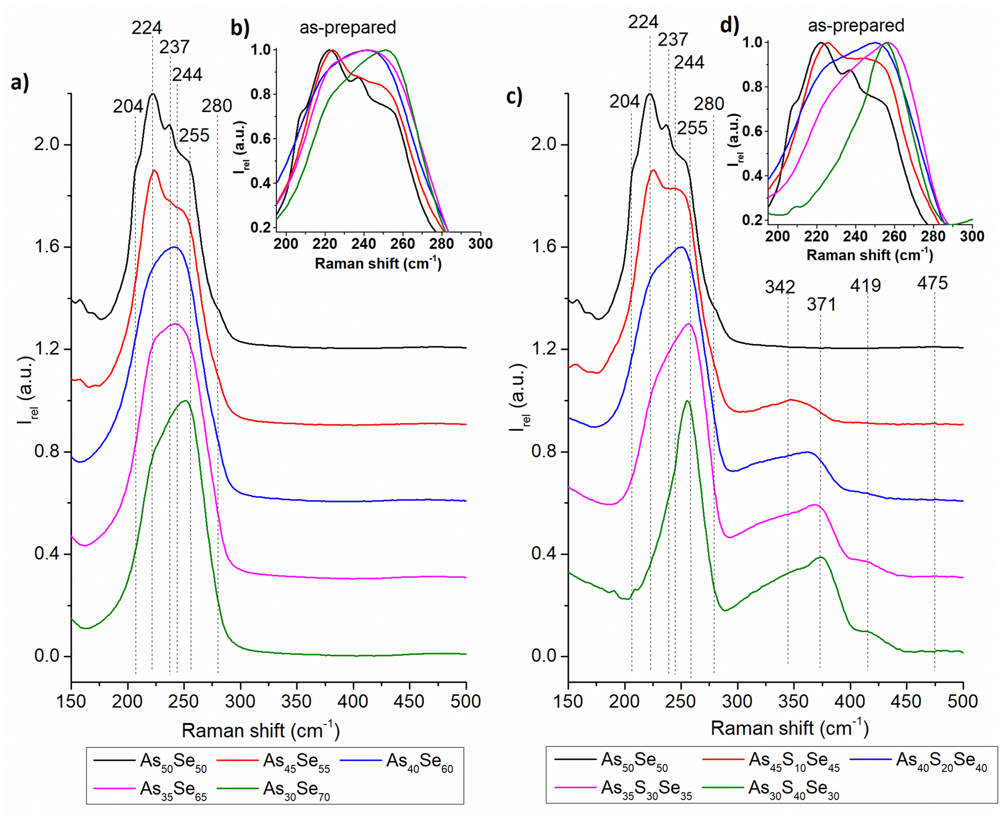 | ||
| Fig. 4 Raman spectra of as-prepared As50Se50, (a) selenium-modified and (c) sulfur-modified chalcogenide glass thin films. The insets in (b) and (d) show the detail of the main Raman peak. | ||
 | ||
| Fig. 5 Raman spectra of As50Se50, (a) selenium-modified and (c) sulfur-modified chalcogenide glass thin films annealed at 150 °C. The insets in (b) and (d) show the detail of the main Raman peak. | ||
| Wavenumber (cm−1) | Vibration of | Source |
|---|---|---|
| 204 | As–As bond in As4Se4 and As4Se3 | 12, 34 and 38 |
| 224 | AsSe3/2 pyramids | 12 and 34 |
| 237 | As–Se bond in As4Se3 or Se-chains | 12, 34 and 39 |
| 244 | As–Se bond in As4Se4 | 12, 34 and 39 |
| 255 | Se8 rings or As4Se3 | 33, 34 and 38 |
| 280 | –Se–Se– bridges between AsSe3/2 pyramids and As4Se3 | 38 and 39 |
| 342 | As–S bond in AsS3/2 pyramids | 31, 34 and 40 |
| 371 | As–S bond in As4S4 | 31, 34 and 40 |
| 419 | AAAS salts | 41 |
| 475 | S8 rings | 7 and 33 |
| 490 | S-chains | 7 and 33 |
The thin films of the unmodified As50Se50 glass consist of AsSe3/2 pyramids (224 cm−1) accompanied by As4Se3 (204, 237, 255, and 280 cm−1) and As4Se4 (204, 244 cm−1) clusters and Se-chains (280 cm−1) connecting the pyramidal units (Fig. 4 – left). After selenium addition, both As4Se3 and As4Se4 react with added Se, forming additional AsSe3/2 pyramidal units. With further selenium addition, the formation of Se-chains and Se8 rings (255 cm−1) was observed. The Se8 rings possess the most intensive band in the Raman spectra of As35Se65, and As30Se70 thin films, thanks to their high Raman signal cross-section. After annealing, the polymerization of the glass matrix was observed as witnessed by a decrease of Se8 ring (and As4Se3 and As4Se4 clusters in As-rich glasses) contents and an increase in AsSe3/2 and Se-chain (237 cm−1) contents.
In sulfur-modified thin films, the formation of AsS3/2 (342 cm−1) pyramids and As4S4 clusters (371 cm−1) was observed as sulfur replaces selenium in the AsSe3/2 pyramids and As4Se4 clusters (Fig. 4 – right). This is supported by the increased amount of Se8 rings in the sulfur-modified thin films that are formed from released selenium. The formation of alkyl ammonium arsenic sulfide (AAAS) salts was also observed. The presence of S-chains or S8 rings (475 and 490 cm−1 respectively) was not detected probably due to their low concentration (most of the sulfur is used to form the AsS3/2 pyramids, As4S4 clusters and AAAS salts). During annealing, decomposition of AAAS salts (419 cm−1) was observed alongside the further formation of AsS3/2 pyramids from the As4S4 clusters. The annealed thin films generally contain fewer As-rich clusters, Se-chains, Se8 rings and more AsSe3/2 pyramids than their as-prepared counterparts due to glass matrix polymerization. The content of AsSe3/2 pyramids is much lower than that in the case of selenium-modified thin films due to higher affinity of sulfur to arsenic compared to selenium (Fig. 5).
The composition of all thin film samples at all annealing temperatures was verified by EDX measurements. The compositions of as-prepared samples and samples annealed at 150 °C (the highest temperature at which all samples still possessed optical quality) are presented in Fig. 6 and 7, respectively. The compositions of all studied thin films at every annealing temperature are presented in Table S1 of the ESI.† All thin films matched the target composition with deviation lower than 2 at%. The thin films are partially depleted of arsenic probably due to oxidation during transport and subsequent sublimation of arsenic oxide in the SEM vacuum chamber.7 The selenium-modified samples maintained their composition throughout all annealing temperatures. The sulfur-modified samples exhibit 3–5 at% sulfur depletion for samples annealed at the highest temperatures due to the evaporation of non-bonded sulfur.31
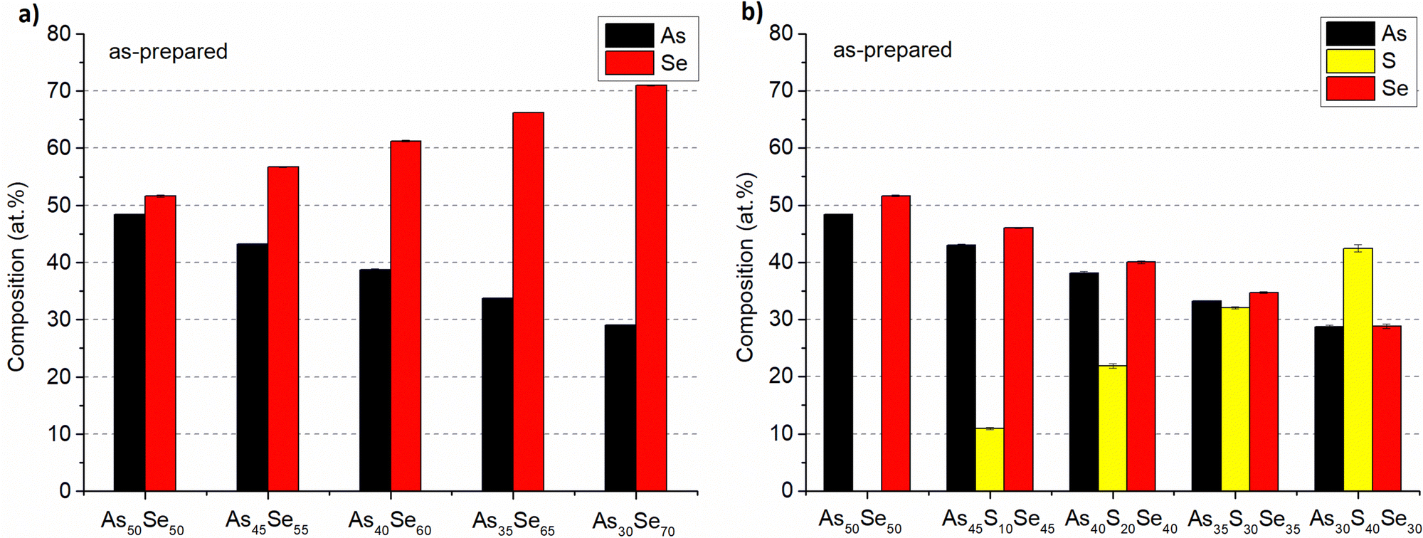 | ||
| Fig. 6 Composition of as-prepared As50Se50, (a) selenium-modified and (b) sulfur-modified chalcogenide glass thin films. | ||
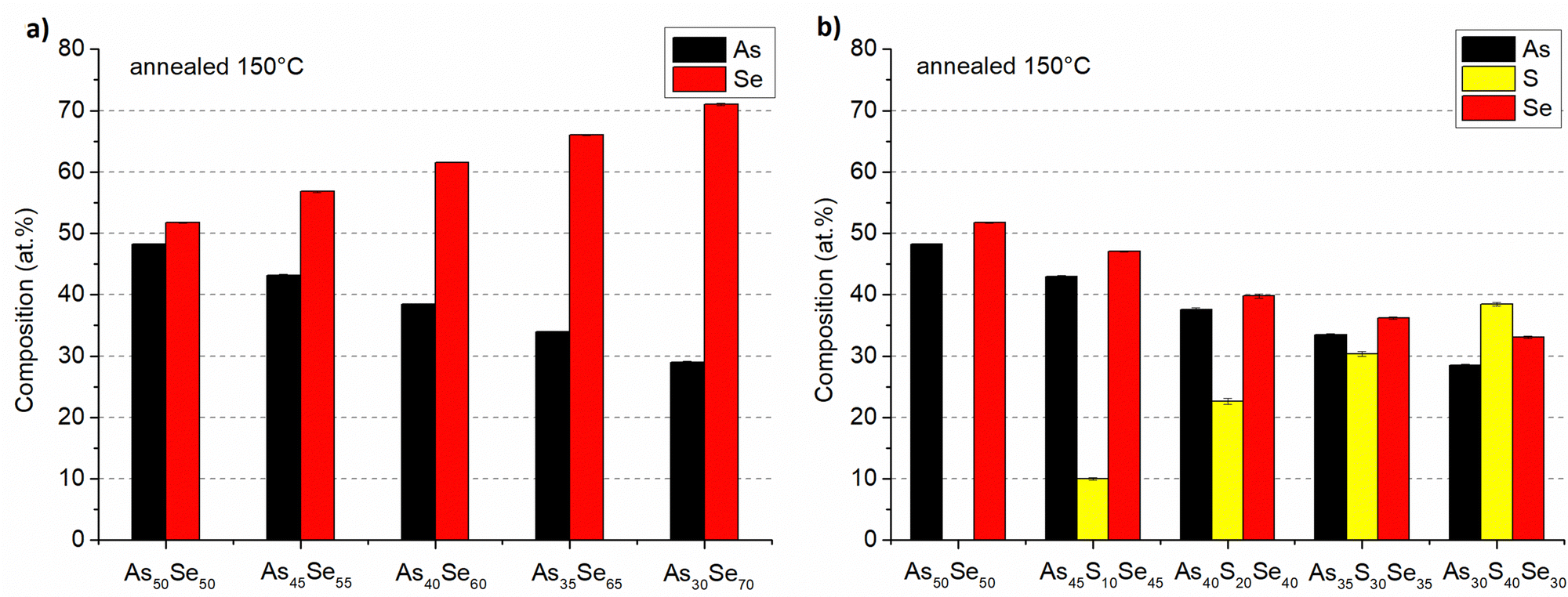 | ||
| Fig. 7 Composition of As50Se50, (a) selenium-modified and (b) sulfur-modified chalcogenide glass thin films annealed at 150 °C. | ||
The organic residual content from the solvent was studied by the EDX measurement of the nitrogen content similarly to our previous work18 and data are presented in Fig. 8. The content of organic residues in thin films annealed at 60 °C gradually grows with the increasing thin film thickness for all studied samples (both S and Se modified). We assume that the organic residual content is affected by the diffusion of the solvent through the thin film and its subsequent evaporation on the surface, because a temperature of 60 °C is well below the boiling point of the used solvent (116–118 °C for ethylenediamine).42 Therefore, in thicker films, the solvent has to diffuse through more materials, most likely leading to a lower overall diffusion rate and a higher organic residual content. It is worth noting that, although the error bars in the mentioned figure are smaller, the resolution of the EDX method for light elements such as nitrogen is about 1%.
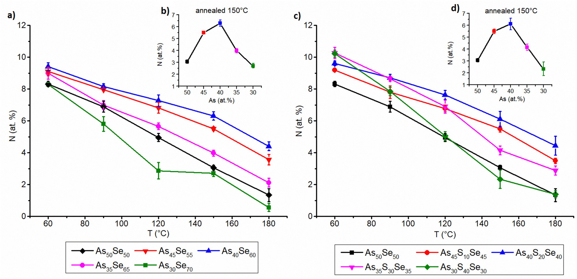 | ||
| Fig. 8 Nitrogen content (proportional to the organic residual content from the solvent) of studied (a) selenium-modified thin films and (c) sulfur-modified thin films depending on the annealing temperature. The insets in (b) and (d) show the dependence of organic residual contents on the composition (shown as arsenic content) for thin films annealed at 150 °C. | ||
The organic residual content in annealed thin films is significantly affected by the proximity of the glass composition to As2X3 stoichiometry. The stoichiometric compositions of both selenium and sulfur-modified thin films (As40Se60 and As40S20Se40) exhibit the highest organic residual content after annealing. The organic residual content gradually decreases with higher (both arsenic and chalcogen) overstoichiometry, due to the less polymerized structure of the overstoichiometric glass matrix. The more compact glass matrix formed from AsSe3/2 pyramids (and AsS3/2 pyramids in the case of sulfur-modified thin films) most likely traps the organic residual in the glass structure and inhibits their release. Both phenomena are closely related, and highly polymerized structures of stoichiometric glasses usually exhibit higher organic residual contents, due to the slower diffusion of solvent through a more compact glass matrix. This is supported by EDX measurements, and Raman measurements are presented above. The release of organic residues can also be affected by lower Tg of overstoichiometric glasses. No significant difference between overstoichiometry of sulfur and selenium was observed regarding this phenomenon.
The thin films of all compositions were deposited in the specular optical quality. The UV-VIS-NIR spectra of prepared thin films are presented in Fig. S2 of the ESI.† The SEM scans presented in Fig. S3 of the ESI,† show no visible defects of thin films regardless of annealing temperature, except for the noticeable crystal growth in highly annealed As50Se50 thin films. Furthermore, the thin films with high chalcogen overstoichiometry (As30Se70 and As30S40Se30) show visible macroscopic degradation due to annealing over their glass transition temperature (Tg ∼ 130 °C).19,26 Due to these reasons, thin films annealed at 180 °C did not possess optical quality and their thickness and optical parameters were not evaluated.
The surface roughness of prepared thin films was studied using atomic force microscopy (AFM). All as-prepared thin films initially show a higher surface roughness than annealed samples of the same composition (Tables 3 and 4).
| T [°C] | As50Se50 | As45Se55 | As40Se60 | As35Se65 | As30Se70 |
|---|---|---|---|---|---|
| 60 | 4.93 ± 0.68 | 5.66 ± 0.52 | 3.81 ± 0.75 | 2.04 ± 0.08 | 1.11 ± 0.12 |
| 90 | 1.79 ± 0.41 | 5.03 ± 0.63 | 5.61 ± 1.32 | 0.69 ± 0.18 | 4.85 ± 1.05 |
| 120 | 0.30 ± 0.04 | 0.43 ± 0.25 | 0.63 ± 0.24 | 0.68 ± 0.21 | 1.25 ± 0.18 |
| 150 | 0.29 ± 0.03 | 0.53 ± 0.39 | 0.25 ± 0.01 | 0.19 ± 0.01 | 0.26 ± 0.01 |
| 180 | 0.4 ± 0.03 | 0.24 ± 0.03 | 0.32 ± 0.04 | 0.26 ± 0.04 | 0.27 ± 0.00 |
| T [°C] | As50Se50 | As45S10Se45 | As40S20Se40 | As35S30Se35 | As30S40Se30 |
|---|---|---|---|---|---|
| 60 | 4.93 ± 0.68 | 5.76 ± 0.29 | 5.48 ± 0.96 | 1.52 ± 0.45 | 7.82 ± 0.53 |
| 90 | 1.79 ± 0.41 | 4.01 ± 0.76 | 9.19 ± 2.64 | 0.33 ± 0.01 | 6.21 ± 0.41 |
| 120 | 0.30 ± 0.04 | 1.09 ± 0.14 | 2.08 ± 0.48 | 0.29 ± 0.04 | 1.89 ± 0.12 |
| 150 | 0.29 ± 0.03 | 0.91 ± 0.42 | 0.58 ± 0.13 | 0.26 ± 0.02 | 2.13 ± 0.40 |
| 180 | 0.4 ± 0.03 | 0.68 ± 0.21 | 1.66 ± 0.74 | 0.28 ± 0.04 | 2.64 ± 0.42 |
The surface roughness does not significantly affect the optical quality of thin film samples as in the case of our previous work.18 The surface roughness decreases with higher annealing temperatures, and all samples annealed at 120 °C or higher temperature possesses a low surface roughness (below 2 nm).
A probable explanation of observed changes in the thin film roughness lies in the tendency to minimize free surface energy via the reduction of the surface area. When the thin film is annealed, the surface diffusion and viscous flow (due to the lower viscosity of the material at higher temperatures) are probably increased. This results in the thin film's flattening (surface area decrease), and consequently the reduction of the surface roughness. More detailed explanation of this phenomenon can be found in ref. 43. The gradual decrease of the surface roughness is also observable from AFM scans, which are presented in Fig. S4 of the ESI.†
The thickness, refractive index at 1550 nm and optical band gap were evaluated using UV-VIS-NIR transmission spectra and are presented in Fig. 9, 10 and 11, respectively. The precise values are provided in Tables S2–S4 of the ESI.† The thickness of selenium-modified thin films is the highest for the stoichiometric glass (As40Se60) and decreases with increasing (both arsenic and selenium) over-stoichiometry (Fig. 9 – left). This may be caused by higher organic residual contents, and therefore the lower thin film density of the stoichiometric glass. With the increasing sulfur content, the thickness of thin films gradually increases, because added sulfur increases the molar concentration of the solution (the same mass concentration was used for all glasses) and probably increases the viscosity of glass solution (Fig. 9 – right). With the increasing temperature, the thickness of thin films gradually decreases due to residual solvent evaporation, AAAS salt decomposition and polymerization of the glass structure as supported by Raman and EDX measurements presented above.
 | ||
| Fig. 9 Dependence of the thin film thickness on the annealing temperature and the thin film composition for (a) selenium-modified thin films and (c) sulfur-modified thin films. The inset graphs in (b) and (d) show the thickness of thin films annealed at 150 °C (the highest temperature at which samples possessed the optical quality) depending on the arsenic content. | ||
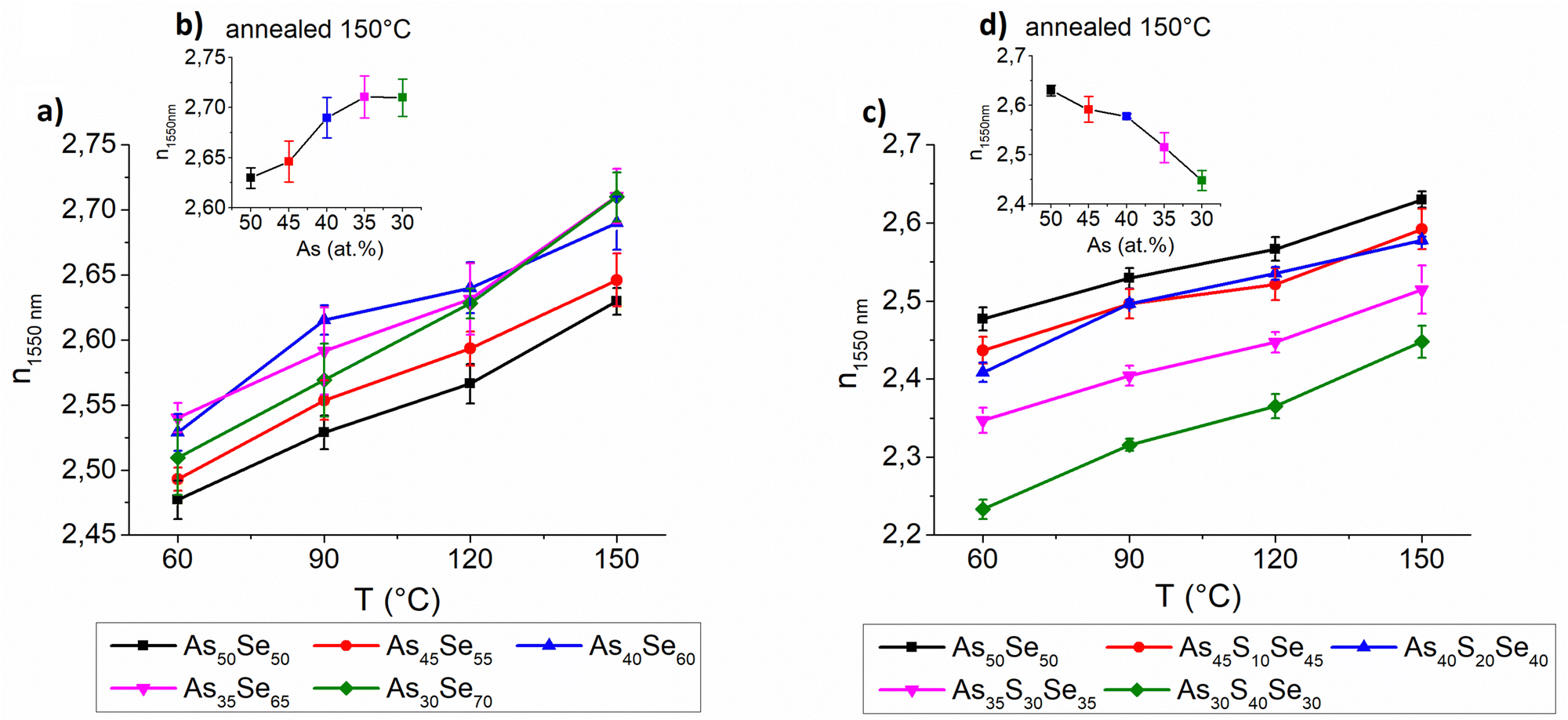 | ||
| Fig. 10 Dependence of the thin film refractive index at 1550 nm at annealing temperatures and thin film composition for (a) selenium-modified thin films and (c) sulfur-modified thin films. The inset graphs in (b) and (d) show the refractive index at 1550 nm of thin films annealed at 150 °C (the highest temperature at which samples possessed the optical quality) depending on the arsenic content. | ||
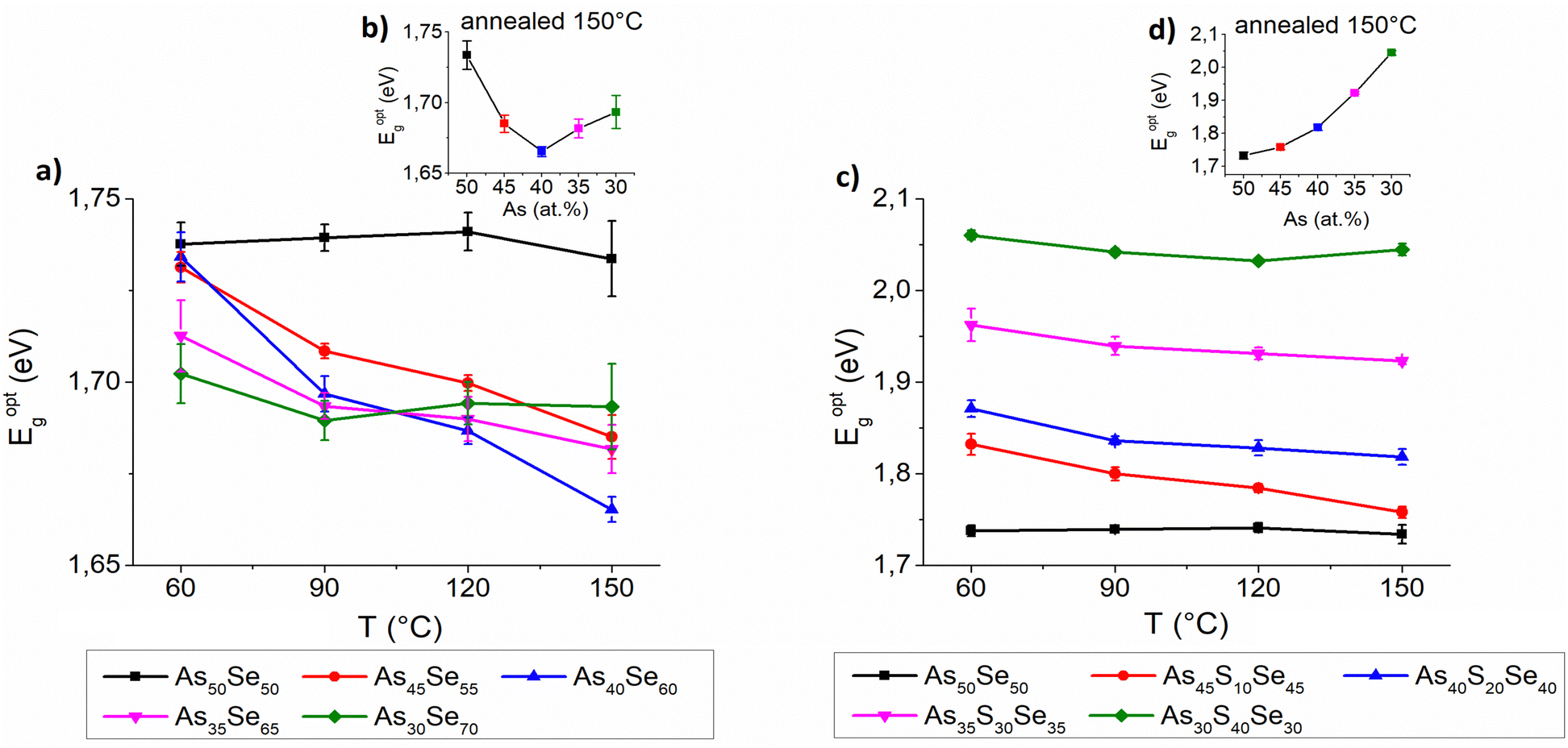 | ||
| Fig. 11 Dependence of the thin film optical band gap on the annealing temperature and thin film composition for (a) selenium-modified thin films and (c) sulfur-modified thin films. The inset graphs in (b) and (d) show the optical band gap of thin films annealed at 150 °C (the highest temperature at which samples possessed optical quality) depending on the arsenic content. | ||
The selenium-modified thin films exhibit the highest refractive index for stoichiometric (As40Se60) and Se-rich thin films while the refractive index of glasses with arsenic overstoichiometry is slightly lower in comparison (Fig. 10 – left). Despite their high organic residual content, the As40Se60 glass possessed a very high refractive index, probably due to the more polymerized glass matrix, compared to the cluster structure of As50Se50, and higher content of selenium (slightly heavier atom). The glasses with high selenium overstoichiometry possessed a high refractive index, due to their low organic residual content and higher content of selenium as witnessed by the EDX measurement above. With the increasing temperature, the thin films exhibit gradual growth in the refractive index and simultaneous reduction of thin film thickness due to solvent evaporation and polymerization of the glass structure.
The sulfur-modified thin films exhibit significant compositional dependence of the refractive index. The increased sulfur content (significantly lighter atom) gradually lowers the refractive index of thin films (Fig. 10 – right). Similar to selenium-modified thin films, with the increasing temperature, sulfur-modified thin films also exhibit gradual growth in the refractive index due to solvent evaporation and polymerization of the glass structure.
The optical band gap of selenium-modified thin films exhibits only minor differences and As50Se50 possessed a slightly higher band gap than other selenium-modified glasses (Fig. 11 – left). In the samples annealed at 150 °C, the band gap is the lowest for the stoichiometric glass (As40Se60) and gradually grows with overstoichiometry. The sulfur-modified thin films exhibit a significant increase of the optical band gap with the increasing sulfur content (Fig. 11 – right) which is in good agreement with already published results.18,23,42 A slight decrease of the optical band gap with higher temperatures was observed in the majority of thin films, probably due to polymerization of the glass structure and release of organic residues and sulfur.
The chemical resistance of thin films was investigated by measuring of the etching rate of thin films in the solution of 5 vol% EDA in DMSO. The gathered data are presented in Fig. 12. The chemical resistance of selenium-modified thin films is the highest (lowest etching rate) for the stoichiometric glass (As40Se60), due to the highly polymerized structure and gradually decreases with increasing overstoichiometry (of both arsenic and selenium). Selenium overstoichiometry lowers the chemical resistance more significantly than arsenic overstoichiometry due to the less polymerized structure of thin films with selenium overstoichiometry (Fig. 12 – left). This claim is further supported by Raman measurements discussed above.
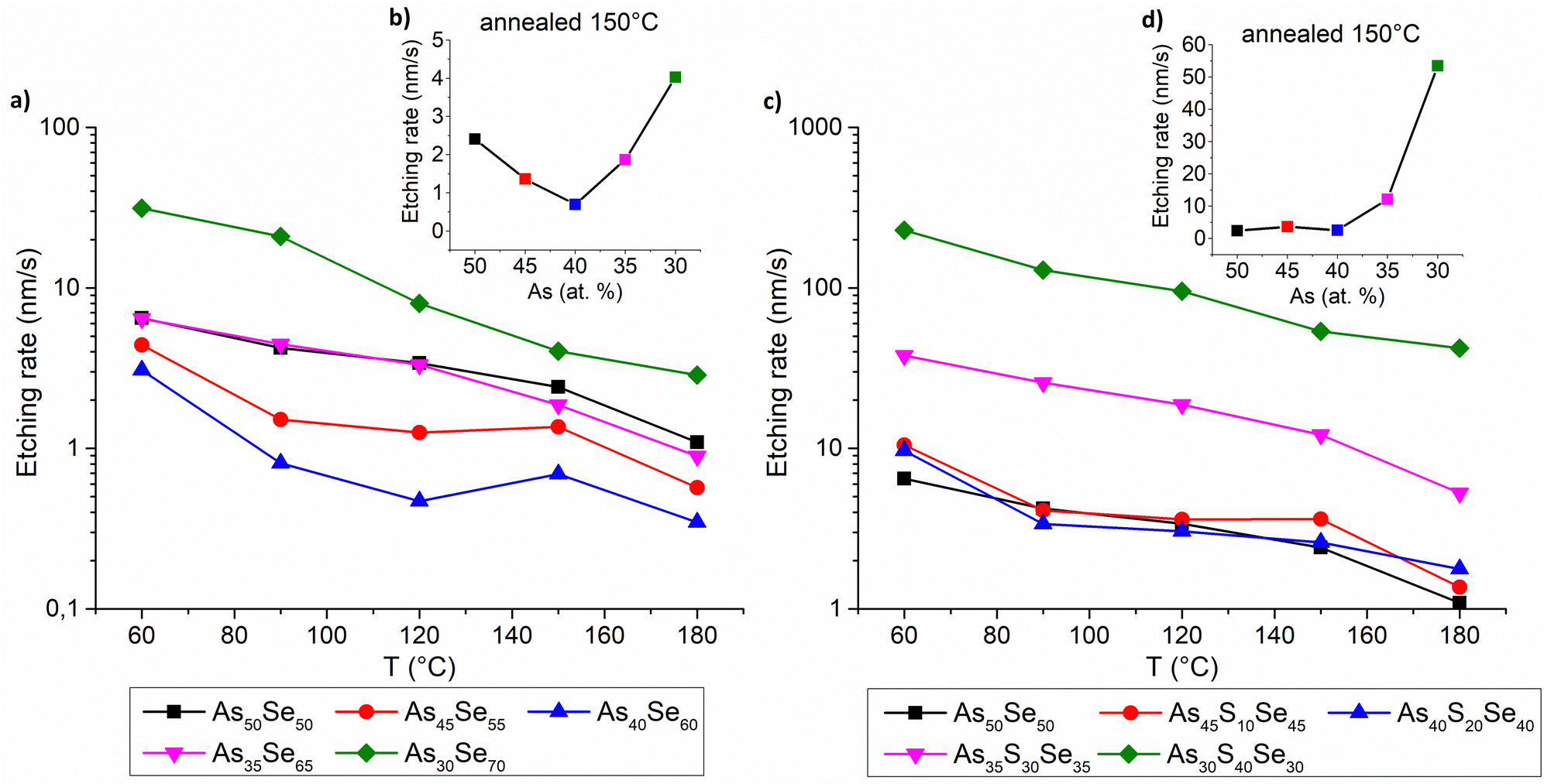 | ||
| Fig. 12 Dependence of the thin film etching rate on the annealing temperature and thin film composition for (a) selenium-modified thin films and (c) sulfur-modified thin films. The inset graphs in (b) and (d) show the etching rate of thin films annealed at 150 °C (the highest temperature at which samples possessed the optical quality) depending on the arsenic content. | ||
The chemical resistance of sulfur-modified thin films is affected by two contradictory phenomena. With the increasing sulfur content, the composition initially gets closer to stoichiometry (more polymerized glass matrix) which increases its chemical resistance (Fig. 12 – right). On the other hand, a higher sulfur content significantly reduces thin film chemical resistance due to the lower chemical resistance of As–S glasses compared to that of As–Se glasses.44 For this reason, the chemical resistance does not change significantly with initial sulfur addition, until the thin films reach stoichiometry (As40S20Se40). With further sulfur addition, the thin films possessed a significantly reduced chemical resistance, because of both the overstoichiometry and the high sulfur content. The detailed structural changes of thin films, responsible for reduced chemical resistance, were previously discussed in the Raman spectroscopy section.
Conclusions
The source solution of the As50Se50 chalcogenide glass in ethylenediamine was modified by elemental sulfur and selenium. Thin films of four sulfur-modified (As45S10Se45, As40S20Se40, As35S30Se35, and As30S40Se30), four selenium-modified (As45Se55, As40Se60, As35Se65, and As30Se70) and unmodified As50Se50 were deposited in a specular optical quality by spin-coating. The chemical structures of prepared thin films, the source solution of As50Se50 and modified solutions were studied using Raman spectroscopy. The data suggest incorporation of elemental chalcogens into the glass structure already in solution.Despite the major differences in the observed chemical structure, selenium-modified thin films exhibit only minor changes in the optical band gap and the refractive index with the increasing selenium content. The biggest difference in both the optical band gap and the refractive index is between As50Se50 and stoichiometric or selenium-rich glasses. Significant changes in the glass structure and organic residual content are observable in chemical resistance, which was studied by the etching of thin films. Stoichiometric glass As40Se60 possessed the highest chemical resistance due to its polymerized structure and lack of homopolar arsenic bonds.
More significant changes were observed in sulfur-modified thin films which exhibit a significant increase in the optical band gap and a decrease in the refractive index with the increasing sulfur content. The addition of sulfur should also decrease the chemical resistance of the thin films, but it also changes the composition of the glass closer to stoichiometry and therefore increases its chemical resistance due to more polymerized glass structure. For this reason, the chemical resistance of thin films remains mostly unchanged for As50Se50, As45S10Se45, and As40S20Se40. With further sulfur addition, the composition changes to chalcogen overstoichiometry and the chemical resistance of thin films decreases significantly.
This method allows the easy modification of thin film compositions and thus the optical and chemical properties of thin films. The solution modification of the bulk glass with arsenic overstoichiometry (As50Se50) offers further insight into the modification mechanism and allows us to study the modified stoichiometric composition and composition with both arsenic and chalcogen overstoichiometry.
This method offers the possibility of preparing a wide range of thin film compositions with different optical properties from a single source solution, which can be beneficial for the cost-effective production of optical elements. The precise tuning of the refractive index and optical band gap can significantly simplify the production of multi-component optical elements, which require several materials with different optical properties.
Author contributions
Jiri Jemelka: conceptualization, investigation, writing – original draft, formal analysis and visualization. Michal Kurka: investigation, methodology, formal analysis, writing – review and editing, and validation. Stanislav Slang: investigation, methodology, formal analysis, writing – review and editing, and validation. Jiri Jancalek: investigation, methodology, formal analysis, writing – review and Editing, and validation. Karel Palka: supervision, validation, writing – review and editing, and resources. Miroslav Vlcek: supervision, funding acquisition, writing – review and editing, and validation.Conflicts of interest
There are no conflicts to declare.Acknowledgements
The authors appreciate the financial support from the grant LM2023037 from the Ministry of Education, Youth and Sports of the Czech Republic.References
- K. Tanaka and K. Shimakawa, Amorphous chalcogenide semiconductors and related materials, Springer, New York, 2021 DOI:10.1007/978-1-4419-9510-0.
- J.-L. Adam and X. Zhang, Chalcogenide Glasses Preparation, Properties and Applications, Woodhead Publishing, 2014 Search PubMed.
- S. Song, S. S. Howard, Z. Liu, A. O. Dirisu, C. F. Gmachl and C. B. Arnold, Appl. Phys. Lett., 2006, 89(4), 041115, DOI:10.1063/1.2236296.
- T. Zhou, X. Liu, Z. Zhu, Z. Liang and X. Wang, Micromachines, 2018, 9(7), 337, DOI:10.3390/mi9070337.
- J. Sheng, Q. Peng, W. Sun, Y. Wang, K. Yang, Z. Feng, J. Wang, G. Wu, J. Wang and K. Jiao, et al. , Opt. Commun., 2022, 513, 128091, DOI:10.1016/j.optcom.2022.128091.
- J. Orava, T. Kohoutek and T. Wagner, Deposition techniques for chalcogenide thin films In Chalcogenide Glasses Preparation, Properties and Applications, Woodhead Publishing, 2014, pp. 265–309 DOI:10.1533/9780857093561.1.265.
- K. Palka, J. Jancalek, S. Slang, M. Grinco and M. Vlcek, J. Non-Cryst. Solids, 2019, 508, 7–14, DOI:10.1016/j.jnoncrysol.2018.12.012.
- T. Halenkovic, J. Gutwirth, P. Nemec, E. Baudet, M. Specht, Y. Gueguen, J.-C. Sangleboeuf and V. Nazabal, J. Am. Ceram. Soc., 2018, 101(7), 2877–2887, DOI:10.1111/jace.15453.
- G. Bulai, O. Pompilian, S. Gurlui, P. Nemec, V. Nazabal, N. Cimpoesu, B. Chazallon and C. Focsa, Nanomaterials, 2019, 9(5), 676, DOI:10.3390/nano9050676.
- S. Slang, P. Janicek, K. Palka and M. Vlcek, Opt. Mater. Express, 2016, 6(6), 1973–1985, DOI:10.1364/OME.6.001973.
- S. Slang, K. Palka, P. Janicek, M. Grinco and M. Vlcek, Opt. Mater. Express, 2018, 8(4), 948–959, DOI:10.1364/OME.8.000948.
- Y. Zou, O. Ogbuu, L. Li, S. Danto, S. Novak, J. Novak, J. D. Musgraves, K. Richardson and J. Hu, Opt. Mater. Express, 2012, 2, 1723, DOI:10.1364/OME.2.001723.
- K. Mokurala, S. Mallick, P. Bhargava, S. Siol, T. R. Klein and M. F. A. M. van Hest, J. Alloys Compd., 2017, 725, 510–518, DOI:10.1016/j.jallcom.2017.07.188.
- P. Arnou, M. F. A. M. van Hest, C. S. Cooper, A. V. Malkov, J. M. Walls and J. W. Bowers, ACS Appl. Mater. Interfaces, 2016, 8(13), 11893–11897, DOI:10.1021/acsami.6b01541.
- J. M. P. Almeida, E. C. Barbano, C. B. Arnold, L. Misoguti and C. R. Mendonça, Opt. Mater. Express, 2017, 7(1), 93–99, DOI:10.1364/OME.7.000093.
- S. Novak, L. Scarpantonio, J. Novak, M. Dai Pre, A. Martucci, J. D. Musgraves, N. D. McClenaghan and K. Richardson, Opt. Mater. Express, 2013, 3(6), 729–738, DOI:10.1364/OME.3.000729.
- M. V. Kovalenko, R. D. Schaller, D. Jarzab, M. A. Loi and D. V. Talapin, J. Am. Chem. Soc., 2012, 134(5), 2457–2460, DOI:10.1021/ja2087689.
- J. Jemelka, K. Palka, J. Jancalek, M. Kurka, S. Slang and M. Vlcek, J. Non-Cryst. Solids, 2023, 605, 122159, DOI:10.1016/j.jnoncrysol.2023.122159.
- Z. U. Borisova, Glassy Semiconductor, Springer, New York, 1981 DOI:10.1007/978-1-4757-0851-6.
- V. Lyubin, M. Klebanov, I. Bar, S. Rosenwaks, N. P. Eisenberg and M. Manevich, J. Vac. Sci. Technol., B: Microelectron. Nanometer Struct.–Process., Meas., Phenom., 1997, 15(4), 823–827, DOI:10.1116/1.589492.
- S. Shtutina, M. Klebanov, V. Lyubin, S. Rosenwaks and V. Volterra, Thin Solid Films, 1995, 261(1), 263–265, DOI:10.1016/S0040-6090(95)06515-6.
- S. Tzadka, N. Ostrovsky, E. Toledo, G. Le Saux, E. Kassis, S. Joseph and M. Schvartzman, Opt. Express, 2020, 28(19), 28352–28365, DOI:10.1364/OE.400038.
- T. Kohoutek, T. Wagner, M. Vlcek, M. Vlcek and M. Frumar, J. Non-Cryst. Solids, 2006, 352(9), 1563–1566, DOI:10.1016/j.jnoncrysol.2005.09.040.
- K. Palka, S. Slang, J. Buzek and M. Vlcek, J. Non-Cryst. Solids, 2016, 447, 104–109, DOI:10.1016/j.jnoncrysol.2016.05.042.
- T. Cardinal, K. A. Richardson, H. Shim, A. Schulte, R. Beatty, K. Le Foulgoc, C. Meneghini, J. F. Viens and A. Villeneuve, J. Non-Cryst. Solids, 1999, 256–257, 353–360, DOI:10.1016/S0022-3093(99)00524-4.
- Y. Zhang and X. Xu, Int. J. Thermophys., 2020, 41, 149, DOI:10.1007/s10765-020-02734-4.
- R. Swanepoel, J. Phys. E: Sci. Instrum., 1983, 16(12), 1214, DOI:10.1088/0022-3735/16/12/023.
- S. H. Wemple and M. DiDomenico, Phys. Rev. B: Solid State, 1973, 3(4), 1338, DOI:10.1103/PhysRevB.3.1338.
- J. Tauc, Mater. Res. Bull., 1970, 5(8), 721–729, DOI:10.1016/0025-5408(70)90112-1.
- M. Vlcek, L. Loghina, K. Palka, J. Buzek and S. Slang, J. Non-Cryst. Solids, 2015, 430, 21–24, DOI:10.1016/j.jnoncrysol.2015.09.021.
- K. Palka, S. Slang, J. Jancalek and M. Vlcek, J. Non-Cryst. Solids, 2019, 517, 76–82, DOI:10.1016/j.jnoncrysol.2019.04.038.
- A. Feltz, Amorphous Inorganic Materials and Glasses, Wiley-VCH, 1993 DOI:10.1002/ange.19941062241.
- S. N. Yannopoulos, J. Mater. Sci.: Mater. Electron., 2020, 31, 7565–7595, DOI:10.1007/s10854-020-03310-0.
- F.-Y. Lin, O. Gulbiten, Z. Yang, L. Calvez and P. Lucas, J. Phys. D: Appl. Phys., 2011, 44(4), 045404, DOI:10.1088/0022-3727/44/4/045404.
- B. Yang, D. J. Xue, M. Leng, J. Zhong, L. Wang, H. Song, Y. Zhou and J. Tang, Sci. Rep., 2015, 5(1), 10978, DOI:10.1038/srep10978.
- C. G. Pantano and T. A. Guiton, Chem. Mater., 1989, 1(5), 558–563, DOI:10.1557/PROC-121-509.
- F. P. Daly and C. W. Brown, J. Phys. Chem., 1975, 79(4), 350–354, DOI:10.1021/j100571a013.
- P. Němec, J. Jedelský, M. Frumar, M. Štábl and Z. Černošek, Thin Solid Films, 2005, 484(1–2), 140–145, DOI:10.1016/j.tsf.2005.02.017.
- K. Shportko, L. Revutska, O. Paiuk, J. Baran, A. Stronski, A. Gubanova and E. Venger, Opt. Mater., 2017, 73, 489–496, DOI:10.1016/j.optmat.2017.08.042.
- A. Stronski, L. Revutska, A. Meshalkin, O. Paiuk, E. Achimova, A. Korchovyi, K. Shportko, O. Gudymenko, A. Prisacar and A. Gubanova, et al. , Opt. Mater., 2019, 94, 393–397, DOI:10.1016/j.optmat.2019.06.016.
- S. Slang, K. Palka, L. Loghina, A. Kovalskiy, H. Jain and M. Vlcek, J. Non-Cryst. Solids, 2015, 426, 125–131, DOI:10.1016/j.jnoncrysol.2015.07.009.
- H. Yu, Q. Ye, H. Xu, X. Dai, X. Suo and R. Li, Chem. Eng. Process., 2015, 97, 84–105, DOI:10.1016/j.cep.2015.09.008.
- W. W. Mullins, J. Appl. Phys., 1959, 30(1), 77–83, DOI:10.1063/1.1734979.
- J. Jancalek, S. Slang, J. Jemelka, M. Kurka, K. Palka and M. Vlcek, J. Non-Cryst. Solids: X, 2023, 17, 100–142, DOI:10.1016/j.nocx.2022.100142.
Footnote |
| † Electronic supplementary information (ESI) available. See DOI: https://doi.org/10.1039/d3ma00614j |
| This journal is © The Royal Society of Chemistry 2024 |