
 Open Access Article
 This Open Access Article is licensed under a Creative Commons Attribution-Non Commercial 3.0 Unported Licence
Photopatternable, degradable, and performant polyimide network substrates for e-waste mitigation†
Caleb J.
Reese
a,
Grant M.
Musgrave
 a,
Jitkanya
Wong
b,
Wenyang
Pan
b,
John
Uehlin
b,
Mason
Zadan
b,
Omar M.
Awartani
b,
Thomas J.
Wallin
*c and
Chen
Wang
*a
a,
Jitkanya
Wong
b,
Wenyang
Pan
b,
John
Uehlin
b,
Mason
Zadan
b,
Omar M.
Awartani
b,
Thomas J.
Wallin
*c and
Chen
Wang
*a
aDepartment of Materials Science and Engineering, University of Utah, Salt Lake City, Utah 84112, USA. E-mail: chen.wang@utah.edu
bReality Labs at Meta, Redmond, WA 98052, USA
cDepartment of Materials Science and Engineering, Massachusetts Institute of Technology, Cambridge, MA 02139, USA. E-mail: tjwallin@mit.edu
First published on 12th July 2024
Abstract
The continuous accumulation of electronic waste is reaching alarming levels, necessitating sustainable solutions to mitigate environmental concerns. Fabrication of commercial electronic substrates also requires wasteful high heat. To this end, we develop a series of reprocessible electronic substrates based on photopolymerizable polyimides containing degradable ester linkages. Five imide-containing diallyl monomers are synthesized from readily available feedstocks to produce high-quality substrates via rapid photopolymerization. Such materials possess exceptional thermal (thermal conductivity, K = 0.37–0.54 W m−1 K−1; degradation temperature, Td > 300 °C), dielectric (dielectric constant, Dk = 2.81–3.05; dielectric loss, Df < 0.024), and mechanical properties (Young's modulus, ∼50 MPa; ultimate elongation, dL/L0 > 5%) needed for flex electronic applications. We demonstrate mild depolymerization via transesterification reactions to recover and reuse the functional components.
Introduction
Recent advances in electronics have led to a widespread global accumulation of electronic waste (e-waste).1,2 Some 54 million tonnes of e-waste, averaging 7.3 kg per person were produced in 2019 alone.1 Continued developments in flexible electronics, i.e., thin, flexible devices made on compliant substrates are inevitable—these devices offer promising opportunities in robotics, wearables, heath monitoring, packaging, and the Internet of Things (IoT).3,4 Unfortunately, the continued adoption of flexible electronics and other low-cost single-use electronics only worsens the dire e-waste situation.5 Awareness of this oncoming catastrophe is evident in the climate initiatives and pledges from some of the largest global hardware manufacturers such as Samsung, Apple, and Google.6–8 Beyond sustainability concerns, there are economic incentives for reprocessing e-waste, since the circuits, such as chip and antenna components, contain high-value resources such as precious metals and rare earth elements. For 2019, estimates of the raw material value in e-waste exceeded 57 Billion USD.9 In many cases, the electronic components would be suitable for a second-life use but recapture remains challenging.2,10Much research approaches the end-of-life issue in electronics by developing new polymeric electronic substrates (e-substrates) with inherent reprocessibility via chemical, thermal, or biological means. In this paradigm, complete degradation or removal of the e-substrate allows for the collection of expensive and reusable electronic components to minimize waste and amortize costs. However, these studies often simplify the circuits design. This simplicity often ignores the stringent material requirements for e-substrates in consumer devices (e.g. high dielectric constant and low dissipation factor for dense circuits and data transfer applications), realities of conventional large-scale device manufacturing (e.g. Pb-free solder reflow processing at ∼250 °C), and the economics of the hardware market (e.g. low raw material and processing costs). For example, several studies report electronic devices built on biodegradable substrates of modified fibrous11,12 or synthetic aliphatic polyesters such as polylactic acid13 and polycaprolactone.14–16 The degradability of these substrates typically comes from the ester linkages undergoing hydrolysis under suitable conditions (heat, oxygen exposure, microorganisms).17 Unfortunately, these polyester systems possess low heat stability well below conventional processing temperatures,18–21 and the conditions for hydrolysis can be so innocuous as to occur in ambient environments leading to premature device failure.11,22 Other work utilized liquid metal circuits printed on top of thermoplastic films to separately recapture the e-substrate, conductive traces, and components.23 Ignoring the inherent concerns with solvent and thermal resistance, thermoplastics are often susceptible to creep and plastic deformation which threaten dimensional stability. Additional shortcomings include that interchain ionic or hydrogen bonds can become active at high frequencies to the detriment of dielectric performance. Recently reported recyclable crosslinked polymers (or “network polymers”) may overcome the drawbacks with high thermal stability. However, the fabrication and reprocessing of these novel thermosets is often costly, requiring multi-step processing that involves solvent evaporation to form films.24–26 As an alternative, crosslinked polyesters can be formed efficiently at room temperature without solvents using mild reaction conditions.27–30
By comparison, polyimide (PI), particularly aromatic polyimides like Kapton®, is a popular substrate in electronic devices due to their unique combination of outstanding mechanical properties including tensile modulus ∼2 GPa; ultimate tensile strength ∼230 MPa; ultimate elongation ∼70%, thermal stability from −250 °C < T < 300 °C; relatively high thermal conductivity ∼0.12 W m−1 K−1; low coefficient of thermal expansion (CTE) ∼ 20 ppm °C−1; high glass transition temperature, Tg > 300 °C, high dielectric constant (Dk or εr), of 3.5 at 1 kHz; and low dielectric loss (Df or tan![[thin space (1/6-em)]](https://www.rsc.org/images/entities/char_2009.gif) δ) of 0.002 at 1 kHz.31,32 Consequently, PIs are ideal substrates for robust, high density, miniaturized circuits, particularly since the superb electrical barrier performance persists in thin film form factors for flexible electronics. Unfortunately, the exceptionally stable imide bonds that help to impart these properties do not readily cleave under mild conditions, limiting reprocessing. Even with the addition of ester linkages, aromatic poly(ester imides) are similarly difficult to degrade.33–37 Another challenge associated with PI substrates is their synthesis. In a typical process, imidization of a polyamic acid solution occurs at exceptionally high temperatures (T = ∼250 °C) and once the resulting solid film forms, photo- and melt-processing becomes prohibitive. As a result, the conventional PI film processing complicates the build-up of multilayered circuit architectures (e.g. application of interlayer adhesives between PI films, laser ablation of PI to form vias, copper deposition for through-plane electrical conductivity) required for dense electronic devices.
δ) of 0.002 at 1 kHz.31,32 Consequently, PIs are ideal substrates for robust, high density, miniaturized circuits, particularly since the superb electrical barrier performance persists in thin film form factors for flexible electronics. Unfortunately, the exceptionally stable imide bonds that help to impart these properties do not readily cleave under mild conditions, limiting reprocessing. Even with the addition of ester linkages, aromatic poly(ester imides) are similarly difficult to degrade.33–37 Another challenge associated with PI substrates is their synthesis. In a typical process, imidization of a polyamic acid solution occurs at exceptionally high temperatures (T = ∼250 °C) and once the resulting solid film forms, photo- and melt-processing becomes prohibitive. As a result, the conventional PI film processing complicates the build-up of multilayered circuit architectures (e.g. application of interlayer adhesives between PI films, laser ablation of PI to form vias, copper deposition for through-plane electrical conductivity) required for dense electronic devices.
Herein, we develop degradable polyimide photopolymers compatible with the existing materials, processing, and application requirements of commercial electronics. We propose using thiol–ene click chemistry as an ideal photopolymerization method for the design of ester-containing networks.38 Despite free-radical polymerization of acrylate or methacrylate free-radical polymerization being a common choice for photopolymerization, it suffers from oxygen inhibition, often resulting in tacky surfaces due to incompletely reacted monomers.39 On the contrary, thiol–ene polymerizations have the benefit of little oxygen inhibition and are proven capable of forming thin films with non-tacky, smooth surfaces.40 Further, many commercially available thiol monomers possess the degradable alkyl ester linkages, like trimethylolpropane tris 3-mercaptopropionate (TMPMP). With respect to thermomechanical properties, we envision imide containing alkene monomers boosting backbone rigidity, resulting in high Tg and high Young's moduli. In this work, we synthesize a family of ester-containing diallyl imides of varying structure derived from commercially abundant chemical feedstocks. We then demonstrate that the photopolymerized thiol–ene polyimide networks result in quality e-substrates with excellent dielectric properties. Depolymerization of these poly(imide ester) networks via transesterification reactions stimulated at ambient temperatures results in successful recovery and reuse of components.
Results and discussion
Synthesis of diallyl bisimide monomers and thiol–ene polymer networks
Reports have shown that linear poly(ester imide)s exhibit excellent e-substrate properties similar to traditional polyimides.36,37 However, to our knowledge there are only two examples in literature of poly(ester imide)s produced by thiol–ene polymerizations. Using thiol–ene polymerization containing imide groups, Shipp et al. showed a maximum Tg of 13 °C with diallyl bisphenone imide and ethylene glycol dithiol monomers, but with no report of mechanical properties; Zhang et al. produced a crosslinked thiol–ene polymer from bis maleimide and trimethylolpropane tris(3-mercaptopropionate) (TMPMP) thiol monomers, showing broad Tg's in the range of 40–90 °C and tensile strength up to 23 MPa.41,42 To fully understand the potential application in electronic substrates, we conduct a thorough investigation of the material property space of bisimide-based thiol–ene polymers. We aim to synthesize glassy network polymers with high Tg's, high tensile strength, high resistance to thermal decomposition, and favorable electrical properties.As a preliminary attempt, we used pyromellitic dianhydride to synthesize a diallyl bisimide monomer, since it is one of the most common dianhydride feedstock for polyimide synthesis.43,44 However, the diallyl pyromellitic bisimide possessed a high melting point (Tm) of 220 °C, which recrystallized rapidly, preventing practical use as a liquid resin. Thus, we investigated other dianhydride feedstock chemicals, to obtain diallyl bisimide monomers with lower Tm's. As shown in Scheme S1,† we identified eight dianhydrides and synthesize their corresponding bisimide diallyl monomers, including 4,4′-oxydiphthalic anhydride, 4,4′-(4,4′-isopropylidenediphenoxy)bis(phthalic anhydride), cyclobutane-1,2,3,4-tetracarboxylic dianhydride, benzophenone-3,3′,4,4′-tetracarboxylic dianhydride, and 3,3′,4,4′-biphenyltetracarboxylic dianhydride, ethane-1,2-diyl bis(1,3-dioxo-1,3-dihydroisobenzofuran-5-carboxylate), 1,2,4,5-cyclohexanetetracarboxylic dianhydride, 4,4′-(hexafluoroisopropylidene)diphthalic anhydride. Dianhydride monomers similar to what are used in commercial PI films were explored in order to illicit similar high-performance properties that these films possess. These successful syntheses all resulted in yields over 70%. Three of the monomers were incapable of forming stable liquids similar to the pyromellitic bisimide. Therefore, we chose the remaining five, namely diallyl ester, diallyl ether, diallyl cyclohexane, diallyl diether, and diallyl hexafluoro (structures shown in Fig. 1 legend), which possessed Tm's lower than 160 °C (Fig. S1†). We focus the rest of the study on these remaining five monomers. We chose TMPMP as the thiol monomer to allow direct comparison of each diallyl bisimide monomer with sufficient crosslinking. In the following, we name the poly(imide ester) thiol–ene networks from the five diallyl bisimide monomers as PI-ester, PI-ether, PI-cyclohexane, PI-diether, and PI-hexafluoro.
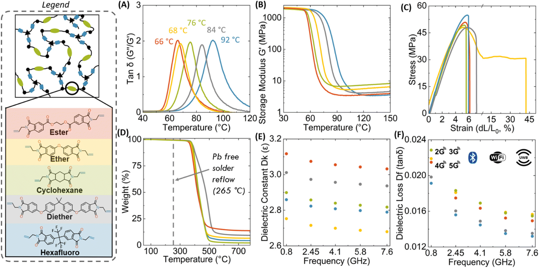 | ||
| Fig. 1 Material characterization of five thiol–ene poly(imide ester) networks synthesized from TMPMP (with 5% excess molar ratio of allyl groups) with ester, ether, cyclohexane, diether, and hexafluoro diallyl bisimide monomers. (A) DMA test revealed that PI-hexafluoro had the highest Tg at 92 °C and PI-ester network had the lowest Tg at 66 °C. (B) Storage modulus by DMA test revealed that all five polymers were covalently crosslinked, showing rubbery plateau's above Tg. (C) Engineering stress–strain curves obtained by tensile test were conducted at ambient conditions (23 °C). (D) TGA tests demonstrated that all polymers were stable at solder reflow temperature (265 °C). (E) Dielectric constant at frequencies from 0.8 to 7.6 GHz showed all five polymers possessed low values from 2.7 to 3.2, sufficient to be used as insulators. (F) Dielectric loss values showed that all five polymers exhibited low losses. Common frequency usage for given frequencies are shown with logos including low frequency cellular networks (0.6–2.1 GHz), Bluetooth (2.4 GHz), Wi-Fi (2.4 and 5 GHz), and ultra-wide band (3–10 GHz). | ||
In our formulation, we added the corresponding diallyl imide in 5 mol% excess to TMPMP (1.05 [C![[double bond, length as m-dash]](https://www.rsc.org/images/entities/char_e001.gif) C]:1 [SH]), and 1 wt% diphenyl(2,4,6-trimethylbenzoyl)phosphine oxide (TPO) as the photoinitiator (Scheme 1A). The excess diallyl imide ensures a quantitative conversion of the thiol groups, since free thiols can react with metals.45,46 Minimal effects on physical properties were seen when comparing 5% allyl excess polymers to stoichiometric polymers formulations by Tg measurement (DMA) and tensile test. In practice, resulting liquid resins possessed a sufficient pot life (order of minutes or greater) such that transfer into heated (T ∼ 80 °C) silicone molds did not result in any noticeable phase separation or solidification. We then irradiated at 405 nm UV light (5 mW cm−2) and 80 °C for 10 minutes to polymerize the resin. Fourier-transform infrared (FTIR) spectroscopy confirmed complete disappearance of the thiol peak (2569 cm−1) and nearly complete disappearance of the alkene peak (3092 cm−1), shown in Fig. S2.† Monitoring the thiol peak by real-time FTIR confirmed the rapid polymerization kinetics typical in neat thiol–ene photopolymerization systems, achieving 63% thiol conversion within 10 seconds with 5 mW cm−2 light intensity (Fig. S3†). The resulting materials were found to be free-standing, glassy, tough, and transparent films, allowing us to readily handle and flex the films at ∼200 μm film thickness (Scheme 1B).
C]:1 [SH]), and 1 wt% diphenyl(2,4,6-trimethylbenzoyl)phosphine oxide (TPO) as the photoinitiator (Scheme 1A). The excess diallyl imide ensures a quantitative conversion of the thiol groups, since free thiols can react with metals.45,46 Minimal effects on physical properties were seen when comparing 5% allyl excess polymers to stoichiometric polymers formulations by Tg measurement (DMA) and tensile test. In practice, resulting liquid resins possessed a sufficient pot life (order of minutes or greater) such that transfer into heated (T ∼ 80 °C) silicone molds did not result in any noticeable phase separation or solidification. We then irradiated at 405 nm UV light (5 mW cm−2) and 80 °C for 10 minutes to polymerize the resin. Fourier-transform infrared (FTIR) spectroscopy confirmed complete disappearance of the thiol peak (2569 cm−1) and nearly complete disappearance of the alkene peak (3092 cm−1), shown in Fig. S2.† Monitoring the thiol peak by real-time FTIR confirmed the rapid polymerization kinetics typical in neat thiol–ene photopolymerization systems, achieving 63% thiol conversion within 10 seconds with 5 mW cm−2 light intensity (Fig. S3†). The resulting materials were found to be free-standing, glassy, tough, and transparent films, allowing us to readily handle and flex the films at ∼200 μm film thickness (Scheme 1B).
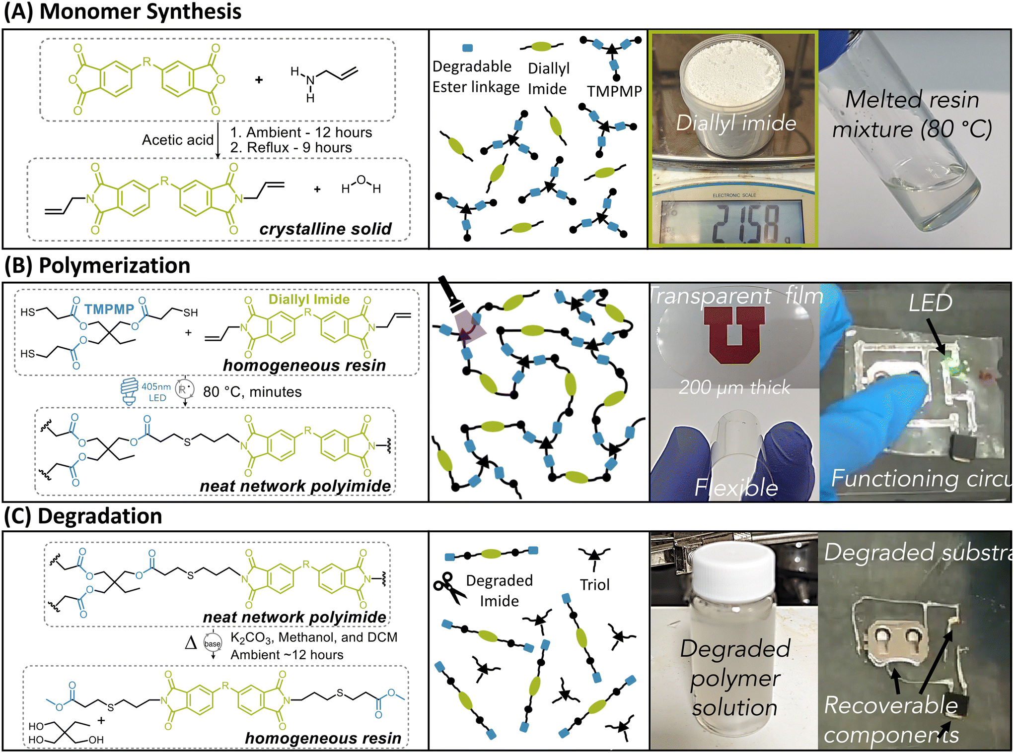 | ||
| Scheme 1 Chemical reaction schemes and example images for monomer synthesis, polymerization reaction, and polymer degradation. (A) Diallyl bisimide monomer synthesis from dianhydride and allyl amine (left). The synthesis is readily scalable in 20-gram batches (right). When mixed with thiol monomer, the thiol–ene resin mixture forms a stable liquid resin. (B) Photopolymerization reaction scheme of a diallyl bisimide monomer and a multifunctional thiol monomer, catalyzed by a free-radical photoinitiator and 405 nm light. The cured film is optically clear, as shown on top of a University of Utah logo and is flexible, as shown above the logo. The film is readily usable as electronic substrates, demonstrated by a functional circuit comprising liquid metal wires, a battery, and an LED bulb. (C) Depolymerization reaction scheme of the polyimide thiol–ene networks by transesterification reaction with methanol, catalyzed by potassium carbonate (K2CO3). The mild depolymerization reaction condition enables recovery of the components. | ||
Thermal, mechanical, and electrical characterization
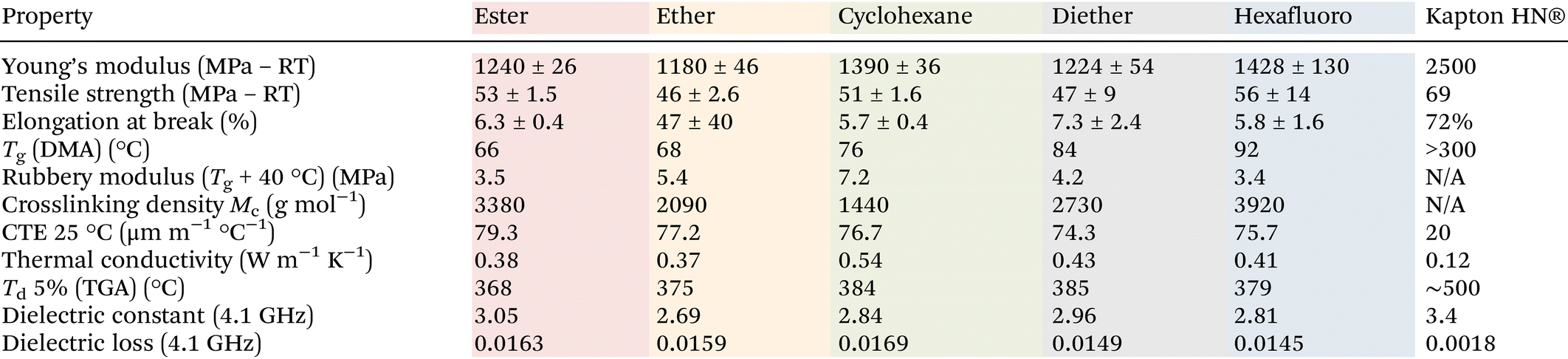
We further investigated the material properties including Tg (by differential scanning calorimetry [DSC] and DMA), tensile strength, dielectric properties, coefficient of thermal expansion (CTE), and thermal stability (by thermogravimetric analysis (TGA)) (Table 1). Varying the diallyl imide monomer resulted in a range of Tg values from 66 to 92 °C (Fig. 1A). Tg values measured via DSC are slightly lower than those from DMA but confirm the same relative trends (Fig. S4†). Notably, the stiff aromatic PI's, PI hexafluoro and PI diether, resulted in the highest Tg values while the aromatic PI's containing flexible linkages of the PI ester and PI ether had the lowest Tg values (Fig. 1, legend). Observing such a structure–property relationship in these networks confirms a high fidelity between our polymer design, synthesis, and processing. While these Tg's are significantly below commercial PI, we believe for wearables, IoT, and single use applications these Tg's are adequate since they are well above the temperature of usage. Additionally, because of the covalent network, dimensional stability is maintained at above Tg, unlike thermoplastics materials that will flow at above Tg. From DMA, PI-cyclohexane has the highest rubbery modulus of 7.2 MPa which suggests an average molecular weight between crosslinks (Mc) of 1440 g mol−1 which is in alignment with PI-cyclohexane possessing the lowest molar mass (Fig. 1B) (Mc calculations can be found in the ESI†). PI-hexafluoro shows the lowest rubbery modulus (3.4 MPa) and the highest Mc of 3920 g mol−1, in agreement with the higher molar mass of the bisimide molecule. From Fig. 1C, the measured Young's moduli range from 1180 MPa to 1428 MPa, with the ultimate tensile strength ranging from 46 MPa to 56 MPa (Table 1). The polymers exhibit moderate extensibility, with elongation-at-break values around 6%, except for PI-ether with an elongation-at-break of 47%, likely due to its flexible ether linkage providing additional backbone mobility. We conclude that all five thiol–ene poly(imide ester) networks are mechanically robust and very capable of serving as e-substrates and with additional formulation and additives allowing for a more direct comparison to commercial polyimides.
|
We quantified the thermal performance of these network polymers by TGA, DSC, CTE, and thermal conductivity. Similar to conventional polyimides, these polymers exhibit high thermal stability, with temperatures for 5 wt% degradation ranging from 368 °C to 385 °C (Fig. 1D and Table 1), far above conventional solder reflow temperatures (265 °C).47 The CTE of the glassy polymers is 74–79 μm m−1 °C−1. Typical polyimide flexible electronic substrates such as Kapton HN® possesses a CTE of 20 μm m−1 °C−1 at ambient conditions. CTE matching between substrate and mounted component is important to mitigate thermal stresses. It is important to note that all polymers exhibit an increase in CTE above their glass transition (see ESI†). Our PEIs also exhibit thermal conductivity ranging from 0.38 to 0.54 W m−1 K−1, which is higher than that of Kapton HN® (0.12 W m−1 K−1).48 Higher thermal conductivity is often desirable for heat dissipation. In fact, our neat photopolymers possess thermal conductivities similar to Kapton MT®, a commercial polyimide which contains additives specifically to improve its thermal conductivity (0.46 W m−1 K−1).49 Together, these thermal properties compare well with commercial polyimides and even outperform in the case of thermal conductivity.
One primary concern for dense electronic circuits is the dielectric behavior of the underlying substrate. Unfortunately, most of the extant literature on reprocessible polymer e-substrates do not quantify it adequately. We measured both the dielectric constant (Fig. 1E) and dielectric loss (Fig. 1F) of our polyimide network polymers at ultra-high frequency regimes relevant to wireless data transfer (Cellular networks, WiFi, Bluetooth, Ultra-wide Band, etc.) At 4.1 GHz, these photopolymers possessed dielectric constants (Dk) ranging from 2.69 (PI-ether) to 3.05 (PI-ester), slightly lower than that of Kapton-NH (3.4). We believe the relatively high dielectric strength of the PI-ester polymer originates from the polar ester groups and could be further accentuated by including high dielectric fillers. Dielectric loss (Df) values were found to range from 0.0145 to 0.0169, which is again comparable to commodity polyimides with dielectric loss values ranging from 0.0037 to 0.020.44 In summary, our materials possess similar dielectric behavior to Kapton, confirming our molecular design motif and further suggesting suitability in extant applications.
Depolymerization and recovery of electrical components
Since the cost of electrical components is usually higher than that of the polymer substrate, recapturing these components under mild and benign conditions to permit reuse is attractive. We hypothesize that the ester groups in the poly(ester imide) network can be targeted by transesterification reactions under mild conditions. Inspired by Cho et al. and our previous work, we stimulate the transesterification reaction with methanol using potassium carbonate (K2CO3) as the catalyst.30,50 As a first attempt, at relevant disc dimension (e.g. 10 mm diameter by 2 mm thick) the depolymerization, although successful, took over a week to complete due to the limited diffusion of methanol into the glassy polymer network. To improve mass transport, we included 50% by volume of dichloromethane (DCM) into the methanol solution which drastically increases the rate of depolymerization. Complete disappearance of the network polymer occurs within 24 hours at ambient conditions for all five polymers with the same sample dimensions. While DCM was used in the study, greener solvents such as THF, ethanol, and ethyl acetate are currently being explored and will be reported on in future work elsewhere.We monitored the depolymerization kinetics by weighing the residual mass of the polymer sample at varied durations. The PI-ester depolymerized the fastest, completing within 12 hours (Fig. 2A). Importantly, PI-ester samples showed little swelling, suggesting that the depolymerization reaction rate exceeded the rate of diffusion. Initially, the other four PI networks showed significant swelling—gaining mass during the first few hours as the solution infiltrates the network—prior to sufficient transesterification disrupting network percolation resulting in broken macroscopic films (Fig. S5†). We hypothesize that PI ester depolymerizes quickly due to the addition of two additional ester linkages within the imide monomer, which are absent in the other four monomers. Chemical analysis using 1H-NMR of the resulting small molecules confirmed the formation of methyl esters at 3.76 ppm shifting from the original mercaptopropionate peak at 4.03 ppm (Fig. S6†). The aromatic ester adjacent proton peaks also shifted from the ester monomer at 4.75 ppm to the degraded monomer's methyl ester location at 3.79 ppm. Thus, we conclude that transesterification with methanol is successful in depolymerizing these poly(imide ester) networks under ambient conditions into methyl ester containing molecules. Much work has been performed using transesterification to repolymerize degraded polyester polymers.51–56 We believe our degraded products are an ideal candidate for repolymerization in a similar manner. However, when similar procedures were used, side reactions occurred. Ongoing work to characterize and repolymerize the degraded molecules using transesterification will be reported elsewhere. As shown in Fig. 2A, the rate of swelling is readily adjustable by controlling the interaction between the solution and polymer (e.g. the cosolvent and its concentration).
 | ||
| Fig. 2 Depolymerization of the PI-ester polymers as substrates, enabling recovery of electrical components. (A) Reaction kinetics show rapid loss of mass for the PI-ester at different concentrations of DCM and methanol using constant 0.07 M K2CO3. The PI ester can be seen to completely degrade within 12 hours with 50 vol% DCM. (B) Snapshots of demonstration of a functioning circuit comprising liquid metal (LM) wires, a battery, a resister, and an LED bulb used for a second life (i). The PI-ester polymer substrate was fully degraded in 2 hours (v), recovering the liquid metal wires and components. The recovered components were used in a new, functioning circuit (vi). It should be noted that the battery was removed before the polymer degradation. The video is included in ESI.† | ||
To demonstrate electronic component recapture via substrate depolymerization, we made films (100 μm thick) from the PI-ester based resin and added a simple routing circuit and basic components. For our conductor, we chose eutectic gallium indium alloys (EGaIn) liquid metal due to its mechanical compliance and more importantly, its recyclability.57 There is a variety of techniques to pattern liquid metal circuits, but in this study we choose selective wetting where a shadow masking combined with physical vapor deposition produces a 20 nm Chromium and 200 nm copper seed layer onto the film into the desired circuit pattern. Then the sample is dip coated into an EGaIn bath.58,59 EGaIn favorably alloys and wets this seed layer to form conductive traces that are deformable (see ESI† for more information). We completed the circuit by attaching electronic components: LED bulb, resistor, R2023 coin cell battery, and battery holder (Fig. 2B). After confirming the circuit is performant, we removed the battery and initiated recapture by immersing the device in the degradation (50% DCM, 50% methanol and 0.07 mol L−1 (M) K2CO3) solution at room temperature. After 2 hours, our PI-ester substrate depolymerized and we observed no visual change of the remaining electronic components. We collected the components, rinsed with isopropyl alcohol and let them dry. We repeated this process for three such circuits and noted that the resistors did not exhibit statistically significant changes in resistance: Ωavg, before = 5.17 ± 0.05 Ω; Ωavg, after = 5.23 ± 0.05 Ω (N = 3) (Fig. 2B-vii). To further confirm functionality after substrate removal, we placed these same components onto a fresh, patterned substrate. This “new” circuit is also performant, as demonstrated by the illuminated LED in Fig. 2. In conclusion, the poly(imide-ester) substrates allow for the fabrication of functional, flexible circuit and the recovery of the components by depolymerizing the substates.
Process compatibility as e-substrates for high density electronics
Pragmatically, solving the e-waste problem by rapidly adopting novel e-substrates only occurs if the underlying technology is compatible with the existing production workflow and infrastructure. Our photopolymer resins allow for direct fabrication of e-substrates in solventless, near-ambient conditions, so we sought to implement these desirable attributes in the fabrication of layered devices. To demonstrate such opportunities for the direct integration, we built bench top devices using our PI-ester based resin that highlights such considerations in scalable manufacturing (Fig. 3A). | ||
| Fig. 3 Demonstration of low-temperature layering fabrication of electronics. (A) The envisioned processing of producing multilayered circuits. Layering starts by adding a conductive material on a preformed PI film using a shadow mask (this could be a doctor bladed UV cured PI film or commercial PI). Components can be placed on the circuit and soldered at the typical 265 °C temperature. Bottom right shows creep strain of the PI-ester using DMA with 0.1 MPa and a 0.1 × 3 × 10 mm sample showing high creep resistance up to 200 °C which demonstrates stability towards high soldering temperatures without flow. Liquid resin is then sprayed onto circuit. A photo mask is used which allows only certain areas of the circuit to be cured (picture of a photopatterned PI film produced on the bottom left in the U logo shape). The initial circuit can then undergo the repeated process producing multilayers in the same manner. (B) The open circuit showed a conductivity at 0.8 Ω of the LM wires (top); the layered circuit showed no conductivity once encapsulated with the PI build layer (bottom). | ||
Today, electronic devices using PI rely predominantly on pre-fabricated PI films due to the inability to liquid-process PI while staying within an acceptable thermal window of many electronic subcomponents. Linear, aromatic PI has prohibitively high Tm (>300 °C) that prevents melt processing, and alternatives based on liquid poly(amic acids) precursors still require imidization steps at >250 °C to initiate ring-closing reactions.43 In order to obtain dense electronic circuits with conventional (i.e., prefabricated PI films) approaches, one would need to build each electronic layer onto a film separately and then align and stack the films. Obtaining the necessary through-layer electronic connections is challenging, requiring additional subtractive steps to “drill” through the substrate to create a “via” and then applying suitable solder to achieve conduction. Electronic components placed on top of the films break 2D planarity and different components are often different heights. Applied liquid “build-up layers” can accommodate this height differential, but interlayer adhesion is problematic. Adhesives also create discrete transitions in stiffness, threatening overall flexibility and mechanical reliability.
By contrast, our resins are liquids at ambient temperatures, which permits straightforward deposition, casting, and leveling of thin layers iteratively. As shown in Scheme 1B, we can readily doctor blade and cure films down to 200 microns. Starting with a preformed PI film, we can place conductive traces and components conventionally. The thermal resistance of our PI films permits solder reflow of Pb-free solder at temperatures of 265 °C for 10 min (see Fig. 3A). For packaging, we can then cast more resin to planarize and insulate this electronic layer. In Fig. 3B, an ohmmeter probe on the bare conductive trace of the layer measured R = 0.8 Ω but after recoating and curing of our PI-ester the probe measures an open circuit (R > 108 Ω). Rather than insulating the entire circuit, we can also achieve “redistribution layers” for multilayered circuits. By employing photomasks, we can selectively photopolymerize our PI-ester in desired regions and leave unexposed regions uncured. This additive approach yields the necessary "via" directly; we can simply remove the uncured resin (University of Utah logo, Fig. 3A) and backfill the "via" with a conductor. The next layer's traces and components can then be built conventionally while simultaneously achieving the desired insulation and conductivity with the previous layer. This workflow is repeatable and infinite for an arbitrary number of layers of flexible circuitry. This proposed manufacturing approach significantly reduces the complexity of building multilayered PI based circuits.
Furthermore, we evaluated the dimensional stability of our network polymers. We expected the networks to resist creep deformation given their covalent crosslinking. Creep tests conducted on PI ester showed little strain using film samples in tension, performed at 25 °C, 100 °C, and 200 °C with 0.1 MPa of constant stress. It is worth noting that the dimensional stability at high temperatures is particularly of interest for solder reflow as mentioned above (Fig. 3A). At ambient, 25 °C, a low creep strain of 0.2% after 50 minutes was observed while at 200 °C a creep strain of 5% was found showing high temperature creep resistance. Much of this “creep” however was due to thermal expansion (3.1% from 25 °C to 200 °C) based on calculations using PI ester CTE.
Preliminary chemical supply chain analysis
The production of legacy polyimide uses an aromatic di-anhydride and an aromatic di-amines as the monomers, such as pyromellitic dianhydrides and 4,4′-oxydianiline. Various anhydride and amines have been used in polyimides to adjust the polymer material properties.60 The poly(imide ester) networks access the same library of dianhydrides by converting them into diallyl monomers with a bisimide core. It is worth noting that we have demonstrated that the diallyl monomer synthesis, without process optimization, achieved >70% yield by using stoichiometric allyl amine reagents and no catalyst. To understand the chemical supply chain of our developed photopolymer at commercial scale, we sought to focus on the comparison to the legacy polyimides.Fig. 4A shows the supply chain of aromatic diamine, utilizing aromatic building blocks like benzene and phenol, with nitrogen introduction occurring via oxidation with nitric acid followed by reduction to obtain an aromatic amine (e.g., aniline).61 By comparison, Fig. 4B shows the supply chain of aliphatic amines, typically produced from ammonia exchange with halides, allowing a more straightforward supply chain due to the direct use of ammonia as the nitrogen source.62Fig. 4B also illustrates the supply chain of multifunctional thiol monomers, where mercaptopropionates are derived from mercaptopropionic acid and a multifunctional alcohol by Fischer esterification, a process commercialized by several companies.63 The addition of hydrogen sulfide to acrylic acid produces mercaptopropionic acid, with increasing acrylic acid production from renewable resources making thiol monomers cost-competitive.64–66 Consequently, the poly(imide ester) photopolymer developed in this work is readily scalable, as it uses high-volume, low-cost building blocks.
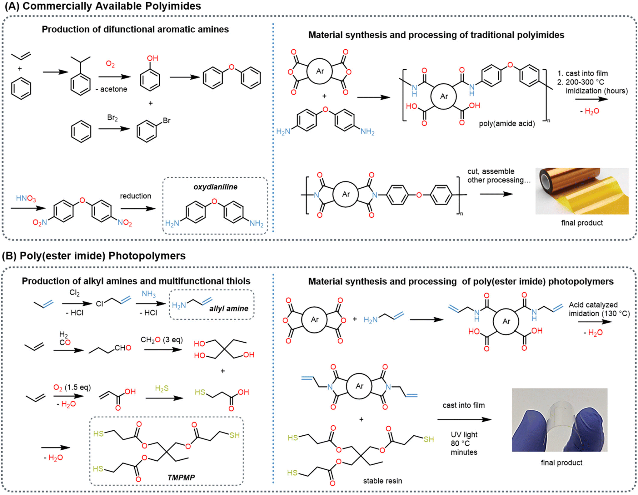 | ||
| Fig. 4 Synthetic production routes of feedstock chemicals for (A) aromatic amines exemplified by 4,4-oxydianiline (right) and synthesis of traditional polyimides (right). (B) Synthesis of alkyl amines and multifunctional thiols exemplified by TMPTMP (left), as well as the polymerization reactions and processing for photopolymerized crosslinked poly(ester imides) (right). The production of aromatic dianhydride is omitted since it is the same for both materials. | ||
Besides monomer costs, material costs include operational expenses. Fig. 4A shows that applying polyimide materials in device fabrication is energy-intensive, as aromatic polyimides have a high Tg (>300 °C) and require imidization between 200 °C and 300 °C over hours.31 In contrast, Fig. 4B depicts the workflow for photopolymerized substrates, which involves simple resin casting and photopolymerization in minutes. This process not only enables advanced manufacturing workflows via photopatterning but also significantly reduces time and energy input at an industrial scale.
Conclusions
In summary, we develop a family of photopolymerizable and reprocessible network polyimides as an alternative to aromatic polyimides such as Kapton® in electronic substrate applications. We synthesized custom diallyl bisimide monomers that participate in thiol–ene photopolymerization and characterization of the resulting polymer networks reveal suitable mechanical strength, thermal stability, thermal conductivity, and dielectric properties, which compare well to commodity polyimides. This framework offers a solution to the growing e-waste problem, since we demonstrate mild depolymerization using transesterification reactions permit the selective removal of the substrate and recovery of still functional electrical components. Most importantly, this photopolymer system integrates well into existing commercial workflows and offers unique advantages towards dense, multilayered circuitry. The chemical feedstocks of such precursors further suggest economic scaling. Thus, we believe this work presents a significant step forward in the development of environmentally friendly materials for electronic applications, contributing to the efforts aimed at addressing the escalating e-waste crisis while maintaining the performance standards required by the industry.It is important to note that the demands of some applications may require further improvements to the material performance and that while comparable, our materials fall short of Kapton along certain metrics. Future investigations could consider adding particulate fillers to further improve the thermal conductivity, thermal expansion coefficient, dielectric constant, etc. Such a straightforward strategy is likely to be successful as commercial polyimide films are often composites. Additionally, our materials are polyimides due to the incorporation of imide groups into our diallyl monomers. We could increase the polyimide character of the backbone by using oligomeric polyimides as precursors, though at the expense of hindered processibility such as increased melting temperature and viscosity. Additionally, we could manipulate the degradation rate by controlling the volumetric density of the ester groups decreases. Finally, future work could focus on further “closing the loop” by repolymerizing the substrate, though the economic motivation for such efforts remains unclear.
Author contributions
Conceptualization: C. J. R. and C. W.; investigation: C. J. R., O. A., J. W., W. P., J. U., M. Z., G. M. M., T. J. W., and C. W.; writing – original draft: C. J. R. and C. W.; writing – review & editing: C. J. R., T. J. W., and C. W.; funding acquisition: C. W.; supervision: C. W.Data availability
The data supporting this article have been included as part of the ESI.†Conflicts of interest
C. W. and C. J. R. have submitted a patent application on degradable electronic substrate polymers.Acknowledgements
This research was supported by the start-up fund provided by the Price College of Engineering at the University of Utah. C. W. and C. J. R. thank Meta Inc for material characterizations. C. W. and C. J. R. thank Anna Huber for assistance with drawing the included cartoons.References
- O. S. Shittu, I. D. Williams and P. J. Shaw, Waste Manage., 2021, 120, 549–563 CrossRef PubMed.
- E. R. Rene, M. Sethurajan, V. Kumar Ponnusamy, G. Kumar, T. N. Bao Dung, K. Brindhadevi and A. Pugazhendhi, J. Hazard. Mater., 2021, 416, 125664 CrossRef CAS PubMed.
- C. Wang, C. Wang, Z. Huang and S. Xu, Adv. Mater., 2018, 30, 1801368 CrossRef PubMed.
- K. Parajuly, R. Kuehr, A. K. Awasthi, C. Fitzpatrick, J. Lepawsky, E. Smith, R. Widmer and X. Zeng, StEP (Bonn), UNU ViE-SCYCLE (Bonn) & UNEP IETC (Osaka), 2019, p. 19 Search PubMed.
- O. Gurova, T. R. Merritt, E. Papachristos and J. Vaajakari, Sustainability, 2020, 12, 8444 CrossRef.
- Samsung Electronics Sustainability Report 2023, https://www.samsung.com/global/sustainability/media/pdf/Samsung_Electronics_Sustainability_Report_2023_ENG.pdf.
- Apple Environmental Progress Report 2023, https://www.apple.com/environment/pdf/Apple_Environmental_Progress_Report_2023.pdf.
- Google Environmental Report 2023, https://www.gstatic.com/gumdrop/sustainability/google-2023-environmental-report.pdf.
- V. Forti, C. P. Baldé, R. Kuehr and G. Bel, The Global E-waste Monitor 2020, 2020 Search PubMed.
- K. Liu, Q. Tan, J. Yu and M. Wang, Circ. Econ., 2023, 2, 100028 Search PubMed.
- Y. H. Jung, T. Chang, H. Zhang, C. Yao, Q. Zheng, V. W. Yang, H. Mi, M. Kim, S. J. Cho, D. Park, H. Jiang, J. Lee, Y. Qiu, W. Zhou, Z. Cai, S. Gong and Z. Ma, Nat. Commun., 2015, 6, 7170 CrossRef PubMed.
- T. Lei, M. Guan, J. Liu, H. Lin, R. Pfattner, L. Shaw, A. F. McGuire, T.-C. Huang, L. Shao, K.-T. Cheng, J. B.-H. Tok and Z. Bao, Proc. Natl. Acad. Sci. U. S. A., 2017, 114, 5107–5112 CrossRef CAS.
- E. Luoma, M. Välimäki, T. Rokkonen, H. Sääskilahti, J. Ollila, J. Rekilä and K. Immonen, J. Plast. Film Sheeting, 2021, 37, 429–462 CrossRef CAS.
- Q. Zhong, X. Chen, Y. Yang, C. Cui, L. Ma, Z. Li, Q. Zhang, X. Chen, Y. Cheng and Y. Zhang, Mater. Chem. Front., 2021, 5, 5371–5381 RSC.
- M. Abdulrhman, A. Zhakeyev, C. M. Fernández-Posada, F. P. W. Melchels and J. Marques-Hueso, Flexible Printed Electron., 2022, 7, 025006 CrossRef CAS.
- S. Liu, Q. Guo, X. Wang, G. Li, X. Ma and Z. Xu, Biosens. Bioelectron.: X, 2022, 11, 100182 CAS.
- Royal Society of Chemistry, Compostable and biodegradable plastics, 2021, p. 606 Search PubMed.
- V. R. Feig, H. Tran and Z. Bao, ACS Cent. Sci., 2018, 4, 337–348 CrossRef CAS PubMed.
- Z. Hui, L. Zhang, G. Ren, G. Sun, H. Yu and W. Huang, Adv. Mater., 2023, 13, 2211202 CrossRef PubMed.
- A. Uva, A. Lin, J. Babi and H. Tran, J. Chem. Technol. Biotechnol., 2022, 97, 801–809 CrossRef CAS.
- M. J. Tan, C. Owh, P. L. Chee, A. K. K. Kyaw, D. Kai and X. J. Loh, J. Mater. Chem. C, 2016, 4, 5531–5558 RSC.
- K. L. G. Ho, A. L. Pometto and P. N. Hinz, J. Environ. Polym. Degrad., 1999, 7, 83–92 CrossRef CAS.
- M. J. Ford, D. K. Patel, C. Pan, S. Bergbreiter and C. Majidi, Adv. Mater., 2020, 32, 1–9 CrossRef PubMed.
- Z. Zou, C. Zhu, Y. Li, X. Lei, W. Zhang and J. Xiao, Sci. Adv., 2018, 4, 1–9 Search PubMed.
- J. Zhang, Z. Lei, S. Luo, Y. Jin, L. Qiu and W. Zhang, ACS Appl. Nano Mater., 2020, 3, 4845–4850 CrossRef CAS.
- J. Zheng, S. F. D. Solco, C. J. E. Wong, S. A. Sia, X. Y. Tan, J. Cao, J. C. C. Yeo, W. Yan, Q. Zhu, Q. Yan, J. Wu, A. Suwardi and Z. Li, J. Mater. Chem. A, 2022, 10, 19787–19796 RSC.
- S. Ma and D. C. Webster, Prog. Polym. Sci., 2018, 76, 65–110 CrossRef CAS.
- W. H. Tham, M. U. Wahit, M. R. Abdul Kadir, T. W. Wong and O. Hassan, Rev. Chem. Eng., 2016, 32, 201–221 CAS.
- W. An, X. Liu, J. Li, X. Zhao, Y. Long, S. Xu and Y.-Z. Wang, J. Hazard. Mater., 2023, 453, 131423 CrossRef CAS PubMed.
- G. M. Musgrave, K. M. Bishop, J. S. Kim, A. C. Heiner and C. Wang, Polym. Chem., 2023, 14, 2964–2970 RSC.
- W. W. Wright and M. Hallden-Abberton, in Ullmann's Encyclopedia of Industrial Chemistry, Wiley-VCH Verlag GmbH & Co. KGaA, Weinheim, Germany, 2000 Search PubMed.
- Physical Properties of KAPTON®, https://mu2e.phy.duke.edu/cw/misc/0404_kapton_properties.cfm.htm.
- T. Iijima, N. Hayashi, T. Oyama and M. Tomoi, Polym. Int., 2004, 53, 1417–1425 CrossRef CAS.
- M. Hasegawa and K. Koseki, High Perform. Polym., 2006, 18, 697–717 CrossRef CAS.
- M. Hasegawa, Y. Tsujimura, K. Koseki and T. Miyazaki, Polym. J., 2008, 40, 56–67 CrossRef CAS.
- S. Mallakpour, P. Asadi and M. R. Sabzalian, Amino Acids, 2011, 41, 1215–1222 CrossRef CAS PubMed.
- S. Mallakpour and S. Soltanian, J. Polym. Res., 2015, 22, 183 CrossRef.
- C. E. Hoyle and C. N. Bowman, Angew. Chem., Int. Ed., 2010, 49, 1540–1573 CrossRef CAS PubMed.
- A. K. O'Brien, N. B. Cramer and C. N. Bowman, J. Polym. Sci., Part A: Polym. Chem., 2006, 44, 2007–2014 CrossRef.
- N. B. Cramer, J. P. Scott and C. N. Bowman, Macromolecules, 2002, 35, 5361–5365 CrossRef CAS.
- K. A. Murphy, A. S. Zebertavage, B. E. Kiliman and D. A. Shipp, J. Polym. Sci., Part A: Polym. Chem., 2013, 51, 4637–4642 CrossRef CAS.
- Y. F. Lu, Y. M. Wang, X. D. Chen, M. H. Miao and D. H. Zhang, eXPRESS Polym. Lett., 2020, 14, 192–204 CrossRef CAS.
- Y.-Y Liu, Y.-K Wang and D.-Y Wu, J. Appl. Polym. Sci., 2022, 139(28), e52604 CrossRef CAS.
- Y. Li, G. Sun, Y. Zhou, G. Liu, J. Wang and S. Han, Prog. Org. Coat., 2022, 172, 107103 CrossRef CAS.
- R. Woods, in Reviews of Physiology, Biochemistry and Pharmacology, Springer Berlin Heidelberg, Berlin, Heidelberg, 1996, vol. 94, pp. 401–453 Search PubMed.
- C. Vericat, M. E. Vela, G. Corthey, E. Pensa, E. Cortés, M. H. Fonticelli, F. Ibañez, G. E. Benitez, P. Carro and R. C. Salvarezza, RSC Adv., 2014, 4, 27730–27754 RSC.
- P. Lall, K. Goyal, K. Schulze and S. Miller, in 2021 20th IEEE Intersociety Conference on Thermal and Thermomechanical Phenomena in Electronic Systems (iTherm), IEEE, 2021, vol. 2021-June, pp. 972–980.
- J. Lawrence, A. B. Patel and J. G. Brisson, Cryogenics, 2000, 40, 203–207 CrossRef CAS.
- D. J. Benford, T. J. Powers and S. H. Moseley, Cryogenics, 1999, 39, 93–95 CrossRef CAS.
- D. D. Pham and J. Cho, Green Chem., 2021, 23, 511–525 RSC.
- Q. Shi, K. Yu, M. L. Dunn, T. Wang and H. J. Qi, Macromolecules, 2016, 49, 5527–5537 CrossRef CAS.
- C. M. Hamel, X. Kuang, K. Chen and H. J. Qi, Macromolecules, 2019, 52, 3636–3645 CrossRef CAS.
- X. Kuang, Q. Shi, Y. Zhou, Z. Zhao, T. Wang and H. J. Qi, RSC Adv., 2018, 8, 1493–1502 RSC.
- X. Kuang, Y. Zhou, Q. Shi, T. Wang and H. J. Qi, ACS Sustainable Chem. Eng., 2018, 6, 9189–9197 CrossRef CAS.
- X. Shi, C. Luo, H. Lu and K. Yu, Polym. Eng. Sci., 2019, 59, E111–E119 CAS.
- T. Liu, B. Zhao and J. Zhang, Polymer, 2020, 194, 122392 CrossRef CAS.
- M. Reis Carneiro, A. T. De Almeida, M. Tavakoli and C. Majidi, Adv. Sci., 2023, 10, 2301673 CrossRef PubMed.
- J. Ma, F. Krisnadi, M. H. Vong, M. Kong, O. M. Awartani and M. D. Dickey, Adv. Mater., 2023, 35, 2205196 CrossRef CAS PubMed.
- K. B. Ozutemiz, C. Majidi and O. B. Ozdoganlar, Adv. Mater. Technol., 2022, 7, 2200295 CrossRef CAS.
- R. G. Bryant, in Ullmann's Encyclopedia of Industrial Chemistry, American Cancer Society, 2014, pp. 1–27 Search PubMed.
- P. Patnaik, A Comprehensive Guide to the Hazardous Properties of Chemical Substances, Wiley, 1st edn, 2007 Search PubMed.
- A. L. Wilson, Ind. Eng. Chem., 1935, 27, 867–871 CrossRef CAS.
- China, CN110872246A, 2020.
- E. W. Dunn, J. R. Lamb, A. M. LaPointe and G. W. Coates, ACS Catal., 2016, 6, 8219–8223 CrossRef CAS.
- D. Sun, Y. Yamada, S. Sato and W. Ueda, Green Chem., 2017, 19, 3186–3213 RSC.
- United States, US5877349A, 1999.
Footnote |
| † Electronic supplementary information (ESI) available. See DOI: https://doi.org/10.1039/d4lp00182f |
| This journal is © The Royal Society of Chemistry 2024 |