
 Open Access Article
 This Open Access Article is licensed under a
 Creative Commons Attribution 3.0 Unported Licence
Surface photovoltage predicts open circuit voltage in GaP/PEDOT:PSS and GaP/CuSCN heterojunction solar cells†
Anna C.
Kundmann
 *,
Kathleen
Becker
and
Frank E.
Osterloh
*
*,
Kathleen
Becker
and
Frank E.
Osterloh
*
Department of Chemistry, University of California, Davis, One Shields Avenue, Davis, CA 95616, USA. E-mail: ackundmann@ucdavis.edu; fosterloh@ucdavis.edu; Fax: (+1)530 752 8995
First published on 20th September 2024
Abstract
The cost-effective fabrication of inorganic photovoltaic (PV) devices is important for their implementation on a global scale. Solution processing techniques, such as spray coating, spin coating, and electrodeposition, can drive down costs; however, a better understanding of the charge transfer characteristics of the resulting semiconductor heterojunctions is needed to minimize photovoltage losses at interfaces. In this work, we generate solution-processed heterojunctions by spin coating PEDOT:PSS and electrodepositing CuSCN as hole transport layers (HTLs) onto GaP wafers. After adding silver paint as a front contact, we obtain devices with short circuit current densities of 0.40 mA cm−2 and 0.18 mA cm−2, open circuit voltages of 0.47 V and 0.43 V, and power conversion efficiencies of 0.045% and 0.031% for PEDOT:PSS and CuSCN HTLs, respectively. Surface photovoltage spectroscopy (SPS) is used to study photochemical charge separation at the illuminated GaP interfaces. We find that the surface photovoltage signal is a good predictor of the photovoltage of the devices, as confirmed by comparison with open circuit potential data. SPS also reveals improved hole collection by the HTLs and a detrimental Schottky junction at the In/GaP back contact, further evidenced by S-shaped current–voltage profiles in electric measurements. Reducing the Schottky barrier height will be essential to improve device performance.
Introduction
Solar power is an essential energy source for meeting the growing global energy demand in a sustainable way. Global cumulative photovoltaic (PV) capacity surpassed 1 TW in 2022, but to meet the 70 TWs of solar energy power demand by mid-century, PV deployment must continue at exponential rates.1–3 To meet this target, low cost, scalable, solution-based PV fabrication methods are highly desired. Spin coating methods are already well established in organic solar cells,4 as well as inorganic absorber (such a lead halide perovskite)5 and inorganic hybrid solar cells.6 For example, the hole transport layer (HTL) poly(3,4-ethylenedioxythiophene):poly(4-styrenesulfonate) (PEDOT:PSS) has been spin coated on Si,7–10 GaAs,11,12 lead halide perovskite,13 and organic14 absorbers to make solar cell devices of reasonable efficiency. Electron transport layers (ETLs) of ZnO or SnO2 have been deposited using similar techniques.15–19 Nanoparticle absorber layers19–21 and silver electrodes made of silver nanowire suspensions22,23 can likewise be prepared using spin-coating techniques. Thus, it is technically feasible to produce solar cells with these low-cost solution-based methods.However, for many absorber materials, the power conversion efficiency of solution-processed heterojunctions still lags behind that of junctions created by chemical or physical vapor deposition, sputtering, or ALD.8,24,25 This is in part because imprecise interfaces between the semiconductor and the electron and hole transport layers introduce charge recombination sites that cause significant voltage losses.7,12,26,27 To overcome this limitation, studies on the charge transfer and charge recombination characteristics of solution-processed interfaces are thus of great interest.
Here we use gallium phosphide (GaP) as a model semiconductor to study photochemical charge transfer at GaP/PEDOT:PSS and GaP/CuSCN interfaces and to manufacture a solar cell. Because of its large bandgap of 2.26 eV, GaP has been a popular absorber for water-splitting photoelectrochemical cells, which require a photovoltage in excess of 1.23 V.28,29 Its use in photovoltaics is less established, likely because the bandgap limits the PCE to 17%.30 However, GaP would make a suitable top absorber in multijunction tandem photovoltaic devices. GaP homojunction PVs have been fabricated with molecular beam epitaxy, photolithography, and electron beam evaporation.31,32 However, demonstrated GaP devices suffer from significant voltage deficits of 0.48 V, requiring further optimization.
Fig. 1a and b show the expected energetic alignment of the components used in this study. The HTLs are p-type materials with Fermi level (EF) positions slightly above the valence band of GaP and are therefore suitable for hole collection from that band. PEDOT:PSS has previously been shown as an effective HTL in the construction of a GaP PV, indicating that solution-processed junctions are a promising avenue for device construction.33
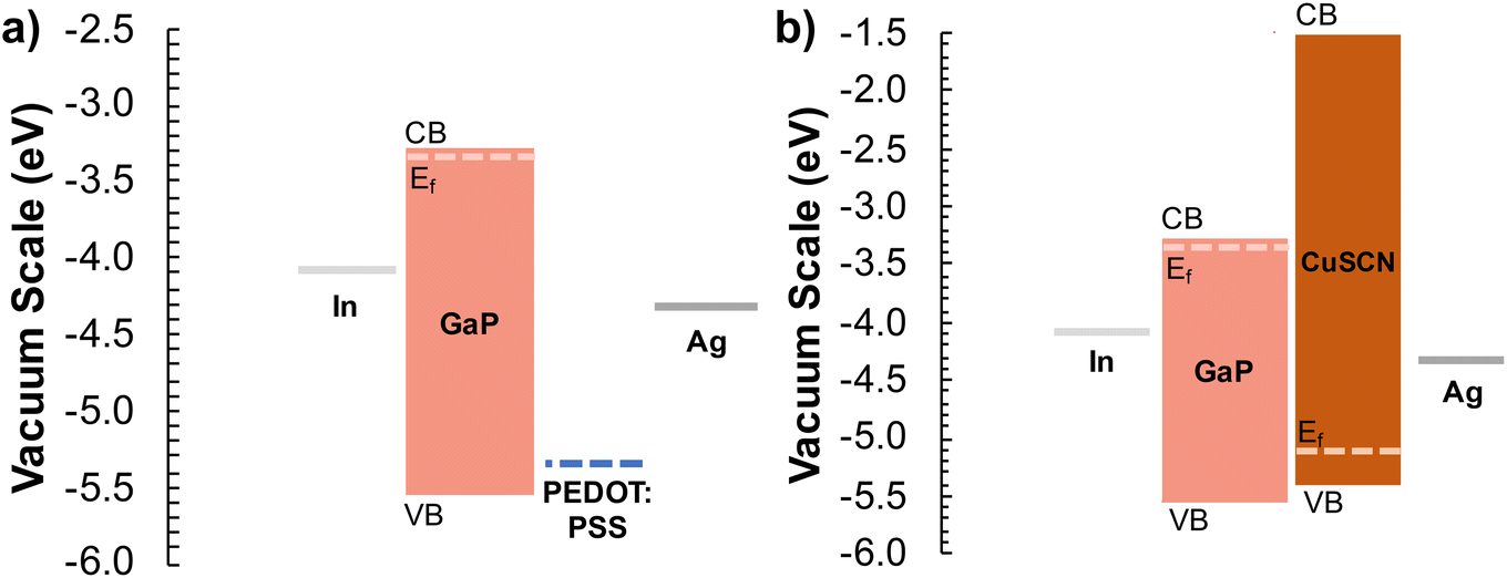 | ||
| Fig. 1 Band energy diagrams depicting band edge alignment of n-GaP-based devices using a) PEDOT:PSS or b) CuSCN HTL. The work function of PEDOT:PSS34 varies (−5.05 to −5.6 eV) depending on fabrication conditions, so an average is shown. Band positions for CuSCN are taken from Treat et al.35 Note the difference in energy scale to accommodate the bandgap of CuSCN. Band edges for GaP are from Van de Walle and Neugebauer.36 Work functions for In and Ag are from the CRC Handbook.37 | ||
We use vibrating Kelvin probe surface photovoltage spectroscopy (VKP-SPS) to estimate the contribution of particular interfaces to the photovoltage of GaP solar cell interfaces in a contactless way for the first time. As we showed recently for BiVO4-liquid junctions,38,39 the surface photovoltage (SPV) signal closely correlates with the VOC in photoelectrochemical cells. Similar correlations are available for silicon, lead iodide perovskite, and organic solar cells in the literature.40–44
We confirm that the light intensity-dependent SPV signals closely match the light intensity-dependent open circuit potential (OCP) in our GaP devices. This further supports the utility of SPS to estimate the photovoltage of partially assembled devices. These findings may have broader implications for other optoelectronic or photocatalytic devices relying on carrier-selective contacts to promote device operation.
Results and discussion
GaP heterojunctions were fabricated as shown in Fig. 2. A commercial sulfur-doped n-GaP wafer was first etched in 3![[thin space (1/6-em)]](https://www.rsc.org/images/entities/char_2009.gif) :1:1 H2SO4:H2O2:H2O at 60 °C for 3 min and indium metal was then soldered on the polished side of the wafer. Next, the HTL (PEDOT:PSS or CuSCN) was coated on the rough side of the wafer within a masked area. Since chemo-mechanical polishing is a costly step in preparing III–V wafers for fabrication of solar cells45 and larger interface area was shown to improve photocurrent in previous GaP/PEDOT:PSS devices,33 we were interested in studying the properties of the larger but less well defined interfaces made at unpolished surfaces. PEDOT:PSS was deposited using the spin coating procedure outlined by Wang et al.,33 with the active area defined by masking tape. CuSCN was applied by electrodeposition from an aqueous solution of 15 mM CuSO4, 67.5 mM diethanolamine (DEA), and 45 mM KSCN using a procedure adapted from Pan et al.,46 with the electrodeposition area defined by polyester tape. A bias of −4.5 V vs. calomel electrode (CE, 3.5 M KCl) was applied for 3 min to produce the CuSCN HTL. Here, the large negative potential is necessary to overcome the electric resistance of the weakly n-doped GaP wafer. Finally, silver paint was applied with a brush around the edge of the mask, leaving a defined active area for illumination (S. Maldonado, personal communication).
:1:1 H2SO4:H2O2:H2O at 60 °C for 3 min and indium metal was then soldered on the polished side of the wafer. Next, the HTL (PEDOT:PSS or CuSCN) was coated on the rough side of the wafer within a masked area. Since chemo-mechanical polishing is a costly step in preparing III–V wafers for fabrication of solar cells45 and larger interface area was shown to improve photocurrent in previous GaP/PEDOT:PSS devices,33 we were interested in studying the properties of the larger but less well defined interfaces made at unpolished surfaces. PEDOT:PSS was deposited using the spin coating procedure outlined by Wang et al.,33 with the active area defined by masking tape. CuSCN was applied by electrodeposition from an aqueous solution of 15 mM CuSO4, 67.5 mM diethanolamine (DEA), and 45 mM KSCN using a procedure adapted from Pan et al.,46 with the electrodeposition area defined by polyester tape. A bias of −4.5 V vs. calomel electrode (CE, 3.5 M KCl) was applied for 3 min to produce the CuSCN HTL. Here, the large negative potential is necessary to overcome the electric resistance of the weakly n-doped GaP wafer. Finally, silver paint was applied with a brush around the edge of the mask, leaving a defined active area for illumination (S. Maldonado, personal communication).
 | ||
| Fig. 2 Fabrication steps for n-GaP-based devices. Indium (In) is used as the back contact while silver paint is used as the front contact (Ag). | ||
Scanning electron microscopy images of the unpolished n-GaP wafer before and after addition of the HTLs are shown in Fig. 3. The unpolished wafer shows a rough surface morphology, as expected (Fig. 3a). The PEDOT:PSS film is shown in Fig. 3b with the contours of the underlying wafer visible and no apparent discontinuities in the film observed. The electrodeposited CuSCN appears as a layer of small (200–300 nm) particles (Fig. 3c). A cleaved film of CuSCN on GaP shows that the particles are in close contact with the rough GaP surface to form the interface studied in this work (Fig. S1†). The energy dispersive X-ray spectroscopy (EDS) data for the GaP wafer and the HTL films on GaP are shown in Fig. S2.† Uncoated n-GaP shows a small surface carbon contamination. EDS of the PEDOT:PSS-coated wafer reveals a high amount of C and O with a trace amount of S, indicating that PEDOT:PSS was successfully deposited on the n-GaP surface. In the CuSCN-coated wafer, Cu, S, C, and N are all present, but not in the ratio expected for CuSCN. Specifically, there is a much higher amount of Cu indicated in the EDS data. Therefore, X-ray diffraction (XRD) was additionally employed to verify the composition of the film. Initial attempts did not yield clear XRD peaks associated with CuSCN because the films were too thin. Therefore, a thick CuSCN film was deposited at the same applied bias (−4.5 V vs. 3.5 CE) for 12 min, instead of 3 min, and an XRD pattern was recorded (Fig. 4). Indeed, this thicker film displays XRD peaks that match the known β-CuSCN phase. However, there is a diffraction peak at 43.5°, indicating that copper metal is also present, consistent with the EDS data. This copper formed by reduction of CuSO4 during deposition of the CuSCN layer. We believe the metallic copper is primarily present at the top surface of the films, as we have found some tendency for the copper to form clusters on the surface of some electrodeposited CuSCN films (Fig. S3†). When comparing the EDS results of areas with clusters to areas without clusters, we find that the Cu amount is about 6-fold higher in the cluster, while the other lighter elements change by <5%. While we cannot entirely rule out the presence of some metallic copper at the GaP/CuSCN interface, we do not believe this to be the main constituent present. It is unclear whether this is a benefit to devices, from enhanced conductivity, or if this is a detriment, resulting in decreased charge carrier selectivity. Finally, XRD confirms the (100) orientation of the GaP wafer, as seen by the high peak intensity at 32.9°.
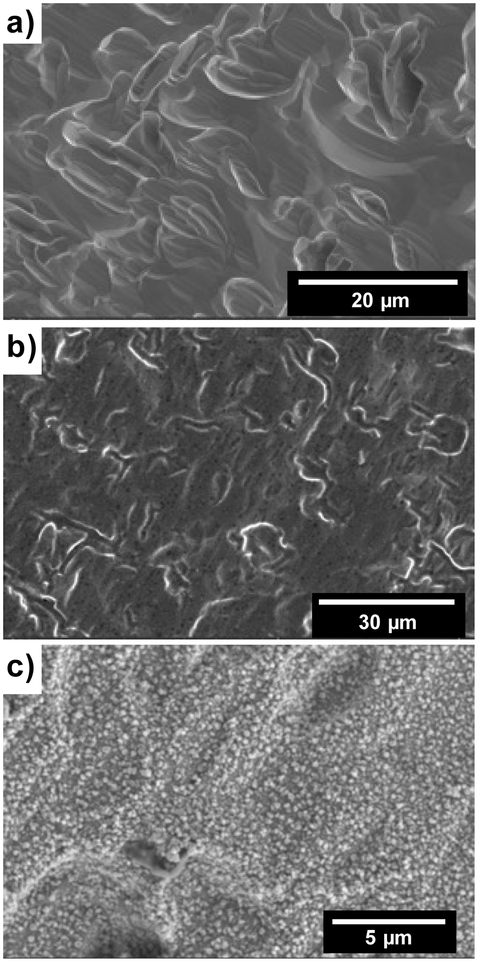 | ||
| Fig. 3 Scanning electron micrographs of unpolished GaP wafer surface (a), PEDOT:PSS film on GaP (b), and CuSCN particle film on GaP (c). | ||
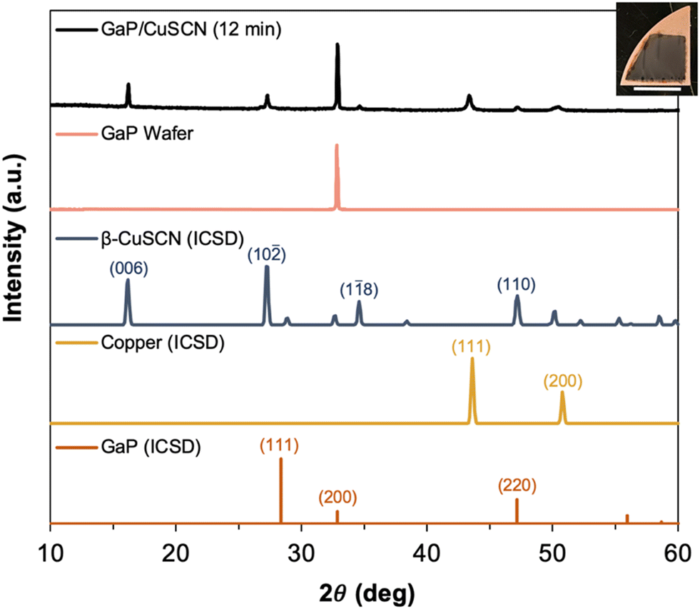 | ||
| Fig. 4 XRD pattern of a CuSCN film deposited on n-GaP for 12 min at −4.5 V vs. 3.5 CE (black line). An image of the sample is shown in the upper right corner (scale bar = 1 cm). The XRD pattern for an uncoated GaP wafer is shown in pink. The 32.9° peak for GaP is enhanced due to the (100) orientation of the wafer. Standard XRD patterns for β-CuSCN (ICSD collection code #24372; dark blue), copper metal (ICSD coll. code #7954; dark yellow), and GaP (ICSD coll. code #635041; dark orange) are shown for comparison with their Miller indices. | ||
UV-vis diffuse reflectance spectroscopy was used to observe the optical properties of the samples.47,48 The spectrum for the GaP wafer in Fig. 5 shows a broad absorption above 620 nm (<2 eV) and an absorption shoulder at 560 nm (2.2 eV). The former corresponds to the free carrier excitation of the S-doped wafer,49 whereas the latter is the bandgap absorption of GaP. Addition of the PEDOT:PSS film enhances the absorption above 620 nm, which is caused by bipolarons, a feature of PEDOT films doped with PSS.50,51 Similarly, the CuSCN film contributes to light absorption at 600–900 nm, likely due to the presence of copper metal in the film, as the bandgap of CuSCN exceeds 3.8 eV.52 This is expected to reduce light reaching the GaP wafer (shading). Overall, the spectra of the modified wafers are the sum of the spectra of the individual components.
 | ||
| Fig. 5 Kubelka–Munk transformation (F(R) = (1 − R)2/2R) of the UV-vis diffuse reflectance spectra of PEDOT:PSS–n-GaP (blue), CuSCN–n-GaP (orange), and n-GaP wafer (pink). | ||
In order to observe the effect of the HTLs on charge separation, vibrating Kelvin probe surface photovoltage spectroscopy (VKP-SPS) was employed. VKP-SPS measures the contact potential difference (CPD) with a Kelvin probe oscillating 1 mm over the specimen. Sample illumination through the semi-transparent probe produces a surface photovoltage signal SPV = CPD(light) − CPD(dark), whose size and polarity provides information about the effective bandgap of the material and the charge carrier separation direction.53–56 For solar cells, it has been shown that the SPV signal closely tracks the VOC.38,40–44 That makes it possible to use VKP-SPS to observe contributions of the individual interfaces to the total VOC.40,41,43,57
SPV spectra for the GaP wafer before and after modifications are plotted in Fig. 6. All spectra show a discontinuity at 2.1 eV that is the result of an optical filter change. While this obscures the 2.26 eV bandgap of GaP,58 it does not affect the diagnostic value of the data. For the n-GaP wafer, the SPV signal is negative, and reaches a maximum of −350 mV at 2.9 eV, where GaP absorbs light and the intensity of the Xe arc lamp is greatest. According to the scheme in Fig. 7a, the SPV is caused by photogenerated charge carriers separated by the depletion layer at the GaP surface, which causes photoholes to move towards the GaP surface/Kelvin probe.
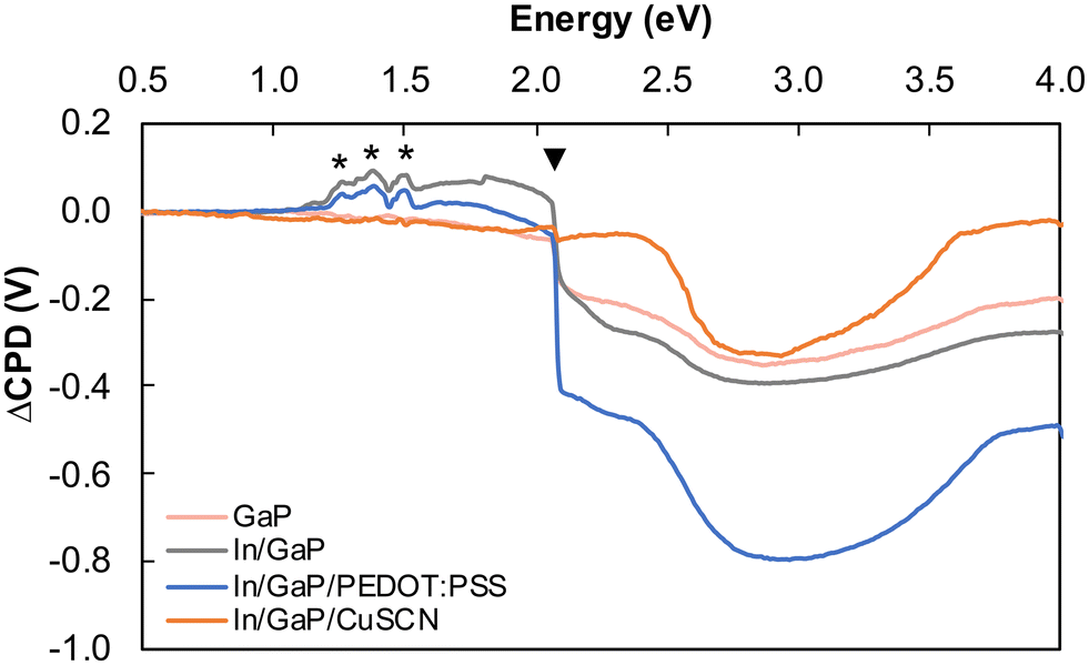 | ||
| Fig. 6 Surface photovoltage spectra of etched n-GaP wafer (pink), n-GaP wafer with In back contact (grey), PEDOT:PSS–n-GaP (blue), CuSCN–n-GaP (orange). Samples with HTLs applied have In as a back contact. Asterisks (*) denote Xe emission lines and triangle (▼) filter change at 2.1 eV. Conditions: air, Xe arc lamp, (1–10 mW cm−2 irradiance at the sample). | ||
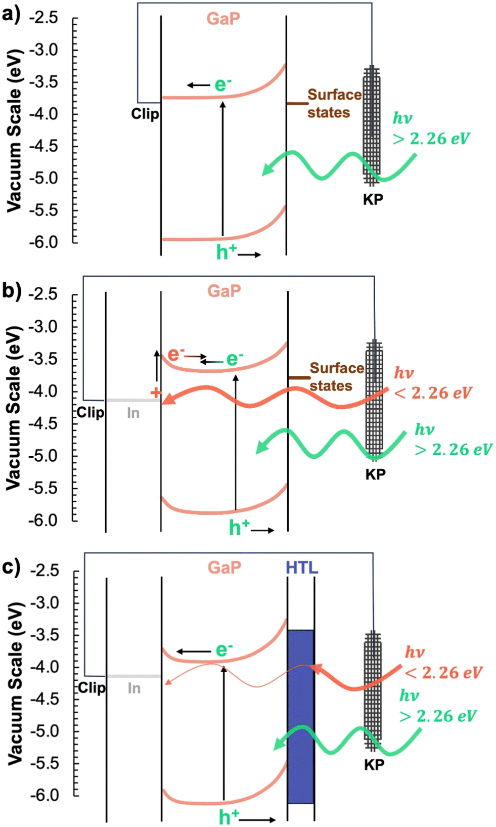 | ||
| Fig. 7 Schematic band diagrams of GaP (a), In/GaP (b), and In/GaP/HTL (c) layer stacks with charge separation based on surface photovoltage spectra. KP stands for Kelvin probe. | ||
Application of the indium back contact does not cause significant changes in the negative photovoltage but introduces a positive (+90 mV) sub-bandgap signal at 1–2 eV. Note that the SPV fine structure at 1.2–1.6 eV is an artifact of the characteristic emission lines from the Xe arc lamp, and the onset around 2.5 eV corresponds to an increase in the monochromated light power (Fig. S4†). The positive sign of the sub-bandgap signal indicates that electrons are repelled by a Schottky-type junction as shown in Fig. 7b. We have previously demonstrated a similar SPV signal inversion due to the formation of a depletion layer between thin particle films and their conductive substrates.57,59 In the present case, the positive signal is generated by photons that are only weakly absorbed by the GaP wafer and that can excite sub-bandgap states at the In/GaP back contact. These states may involve In–P species formed at the GaP–In interface.
When PEDOT:PSS is added to the GaP front, the negative SPV signal increases by a factor of 2, indicating improved hole transfer to the front. This is due to the ability of PEDOT:PSS to accept and conduct positive charge carriers (Fig. 7c). Additionally, the sub-bandgap signal is decreased, which is attributed to a shading effect from the HTL. This shading effect is caused by the 1–2 eV parasitic light absorption from PEDOT:PSS, as seen in in the UV-vis spectra in Fig. 5. Lastly, the SPV spectrum for the CuSCN-coated GaP wafer is also shown in Fig. 6. It is similar to that for the PEDOT:PSS–n-GaP sample, except the negative photovoltage is smaller than for the unmodified GaP wafer, and the SPV onset is shifted to 2.5 eV. Both changes are a result of parasitic light absorption by CuSCN in the 1.5–3.0 eV regime, as confirmed by the absorption spectrum in Fig. 5.
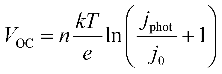
To investigate the intensity-dependent photovoltage of GaP in contact with the HTLs, SPV data were collected under intermittent 405 nm (3.1 eV) illumination, where GaP absorbs all incident light (Fig. 8a and b). The photovoltage is negative, in agreement with the spectra in Fig. 6 and the model in Fig. 7. The SPV signal forms reversibly and increases with light intensity. Time constants for SPV formation and decay are, respectively, 10 s and 15 s for PEDOT:PSS–n-GaP and 10 s and 10 s for CuSCN–n-GaP, with the time resolution limited by the 5 second time interval between data points. This is much faster than what is found for thin films of metal oxides.60 It is a result of the high mobilities of the electrons (160 cm2 V−1 s−1) and holes (135 cm2 V−1 s−1) in gallium phosphide.61 A very minor drift of the CPD baseline to positive values is evident for the CuSCN–n-GaP sample. This suggests trapping of electrons at the front contact, possibly involving reduction of Cu(+) to Cu(0). When the SPV data is plotted versus the logarithmic light intensity, straight lines are observed for both systems. This agrees with the diode equation (eqn (1))62 for a semiconductor junction. This equation predicts a linear increase of the open circuit voltage (VOC, photovoltage) with the logarithmic irradiance. In the equation, k, T, and e have their usual meanings, and jphot and j0 are the photocurrent density and dark reverse bias current density of the junction, respectively.
 | (1) |
 | ||
| Fig. 8 Surface photovoltage (change in contact potential difference [ΔCPD]) and open circuit potential (OCP) measurements of PEDOT:PSS–n-GaP (a and c) and CuSCN–n-GaP (b and d) under variable light intensity (mW cm−2) from a 405 nm LED. White circles indicate when the LED is turned on and black circles indicate when the LED is turned off. Semi-logarithmic plot of OCP and surface photovoltage (SPV) vs. incident light power for PEDOT:PSS–n-GaP device (e) and CuSCN–n-GaP device (f). | ||
To test these VOC predictions, solar cells (images in Fig. S5†) were completed by applying silver paint to the HTLs, as shown in Fig. 2, and open circuit potential (OCP) data were recorded under intermittent 405 nm LED illumination (Fig. 8c and d). As can be seen, the OCP changes quickly under illumination and decays to zero when the illumination is turned off. Signal reversibility and timescales are nearly identical to the behavior seen for the SPV. A plot versus the logarithmic irradiance (Fig. 8e and f) shows that OCP and SPV values track closely across replicate measurements on the same device and across different devices. For example, a second PEDOT:PSS–n-GaP device has a lower SPV compared to the first, which is matched by a degraded VOC and J–V response (Fig. S6†). By contrast, the CuSCN devices showed better consistency across devices in SPV and VOC. Overall, OCP values are within 100 mV of the SPV values. Not surprisingly, the OCP slopes (−0.077 V per decade for the PEDOT:PSS device and −0.150 V per decade for the CuSCN device) are similar to those seen for the SPV data, confirming that SPV is a useful tool for determining the IF and identifying defect-assisted recombination in devices. Overall, this data demonstrates the value of VKP-SPS on semiconductor junctions for predicting VOC of the corresponding assembled solar cells.
To observe the solar power conversion efficiency (PCE), J–V curves were recorded under simulated AM1.5G illumination (Fig. 9 and Table 1). Our PEDOT:PSS device shows a VOC of 0.47 V, short circuit current density (JSC) of 0.40 mA cm−2, fill factor (FF) of 0.24, and PCE of 0.045%. This JSC is more than double the JSC of the planar n-GaP devices fabricated by Wang et al. (see Table 1),33 although, the VOC is lower. This voltage loss appears to primarily be due to the detrimental Schottky barrier observed in the VKP-SPS data from the In–GaP back contact (see discussion below). The CuSCN device shows a VOC of 0.43 V, JSC of 0.18 mA cm−2, FF of 0.41, and PCE of 0.031%. The lower VOC was already apparent in the OCP and SPV measurements, although the monochromatic and AM1.5G illumination conditions are not quantitatively comparable. It is attributed to light shading from the CuSCN layer. Parasitic light absorption by the CuSCN layer also reduces the photocurrent of the GaP–CuSCN device.
 | ||
| Fig. 9 Current–voltage curves for PEDOT:PSS–n-GaP device (blue) and CuSCN–n-GaP device (orange) under simulated AM1.5G illumination. | ||
While devices of reasonable PCE and larger VOC have recently been obtained from Si/PEDOT:PSS heterojunctions,6,66 devices on GaP reported here and previously by Wang et al. have considerable room for improvement. As a wide-bandgap semiconductor, ohmic contacts to GaP can be more difficult to form compared to low-bandgap Si, a key finding in our devices. Additionally, due to the proliferation of Si-based PV, solar-grade Si wafers with very low defect density can be obtained,67 while the lowest-defect III–V materials are made via epitaxial methods not employed in this study. While our devices do not show high performance, they are in line with other reported planar GaP heterojunction solar cells,33 and serve as a reasonable platform for the surface photovoltage measurements that are the main focus of our study.
Lastly, cyclic voltametric scans were recorded to evaluate hysteresis behavior and investigate the electronic operation of the devices. As can be seen from Fig. S7,† while there is minimal hysteresis in the CuSCN device, the PEDOT:PSS device has strong hysteresis behavior, showing a loss of photocurrent under reverse bias during the cyclic scan. This behavior is in contrast to the observation by the Maldonado group for a similar device.33 It is attributed to a photoelectrochemical reaction in the PEDOT:PSS film and at its interfaces with GaP and silver. PEDOT:PSS is known to undergo electrochemical redox reactions in the presence of an electrolyte.68,69 The J–V curves in Fig. S7† also exhibit a very prominent S-shape, seen as the plateau in current at 0.5–1.6 V applied bias, which is degrading the fill factor and photovoltage. By contrast, a typical diode would pass current exponentially in the forward bias direction. The S-shape, also known as “roll-over”, indicates the presence of a barrier to charge extraction at one or more of the GaP contacts, consistent with the presence of a Schottky barrier at the back contact, as revealed in VKP-SPS measurements and depicted in Fig. 7b. This barrier acts like a second diode opposing the main photodiode, requiring more applied bias to achieve charge carrier extraction in either direction, thus degrading the fill factor.70–72 This is a common phenomenon in Si heterojunction,73–75 CdTe,76 organic,77,78 and perovskite79–81 solar cells.
The devices by Wang et al.33 do not show this S-shape, likely due to the forming gas anneal of the In back contact, as such charge transfer barriers are quite sensitive to metal workfunction and interface states. Indeed, VKP-SPS performed on n-GaP with an In back contact that was subjected to a 10 min forming gas anneal at 400 °C shows a near elimination of the positive sub-bandgap SPV (Fig. S8†). It is notable that VKP-SPS detected this Schottky barrier before devices were completed and highlights the utility of VKP-SPS when building photovoltaic device structures. Moreover, while there are slight deviations between the OCP and SPV, the OCP and SPV data clearly show a close correlation, with the SPV response giving a contactless indication of device performance. This holds true despite the S-shape in the J–V plots. This expands on previous works38,39 demonstrating the alignment of SPV and VOC data to include heterojunction devices with charge transfer barriers, showing the robustness of the correlation. Additionally, this is the highest bandgap device studied using this technique. Emerging solar cell device technologies are largely based on heterostructures with many layers needing to align energetically, and VKP-SPS can serve as an initial contactless method to ensure each layer is contributing as expected to the total photovoltage.
Conclusion
Two GaP photovoltaic devices were prepared from n-type GaP wafers by spin coating and electrodeposition of PEDOT:PSS and CuSCN, respectively, and using silver paint and In metal as contacts. VKP-SPS identified a Schottky barrier between n-GaP and In that could be eliminated with forming gas annealing. VKP-SPS further showed that HTLs improve charge separation and there is a close correlation between the SPV signal and the OCP data. Although electrodeposited CuSCN was found to have high parasitic light absorption, it was shown to be a more stable and reproducible HTL than PEDOT:PSS. Devices show power conversion efficiencies of less than 0.05%. The current–voltage curves show strong S-shapes, indicating that the Schottky barrier at the back contact limits the fill factors and power conversion efficiencies of the devices. This work demonstrates the utility of VKP-SPS in diagnosing barriers to charge transfer and contactlessly measuring the photovoltage contribution of each layer to the final operating device. This work provides insight into the formation of carrier-selective contacts on III–V materials without epitaxial growth methods.Experimental
Chemicals
Poly(3,4-ethylenedioxythiophene):poly(4-styrenesulfonate) (PEDOT:PSS; 3.2% w/v in water, Sigma-Aldrich), Triton X-100 (electrophoresis grade, Fisher Scientific), dimethyl sulfoxide (DMSO; ≥99.9%, EM Science), copper(II) sulfate (≥99%, Sigma-Aldrich), diethanolamine (99%, Sigma-Aldrich), potassium thiocyanate (99%, Sigma, Aldrich), GaIn eutectic (99.99%, Sigma-Aldrich), and conductive silver paint (Ladd Research) were used as described in the text without additional modifications. Water was purified to 18 MΩ cm resistivity using a Nano-pure system. n-Type sulfur-doped gallium phosphide wafers (n-GaP, carrier density 4.8–16 × 1017 cm−3, purchased via EL-CAT Inc. from Elma-Malachit) were etched in freshly prepared 3:1:1 solution of H2SO4:H2O2:H2O (piranha acid) at 60 °C for 3 minutes immediately before use. Films on n-GaP were stored in a glovebox with O2 concentration ≤60 ppm.
Spin coating of PEDOT:PSS33
2.5 mL PEDOT:PSS solution, 0.5 mL DMSO, and 0.1 mL Triton X-100 were dissolved in water to produce a total solution volume of 10 mL. The solution was kept in a refrigerator between uses. Spin coating was performed in a model WS-400BZ-6NPP spin coater from Laurell Technologies Corporation connected to a vacuum pump and N2 tank. GaP wafer pieces were taped onto a clean glass slide and the glass slide was secured to the spin coater. Wafer pieces were not directly attached to the holder of the spin coater because it applies a strong suction force that would break the fragile wafer. After substrates were secured to the spinning base, a micropipettor was used to deposit the designated amount of spin coating solution (typically 20–40 μL, depending on substrate size) before the programmed spinning procedure was initiated. Substrates were spun at 500 rpm for 5 minutes and films were left to completely dry. Samples were briefly heated to 100 °C on a hot plate under N2 to drive off residual water.Electrodeposition of CuSCN46
15 mM CuSO4, 67.5 mM diethanolamine (DEA), and 45 mM KSCN were dissolved in water to make the electrodeposition bath. Etched n-GaP was used as the working electrode, with the back polished side and clip contact protected with polyester tape, in a three-electrode set up with a calomel electrode (3.5 M KCl) as the reference electrode and a Pt wire as the counter electrode. A CV scan was first performed to see where cathodic current began to flow. The films were deposited using chronoamperometry set to an applied voltage of −4.5 V vs. 3.5 CE. The current density was approximately −4.7 mA cm−2.Surface photovoltage spectroscopy
Surface photovoltage (SPV) spectra were measured in air. A semitransparent, vibrating gold Kelvin probe (Delta PHI Besocke) served as the reference electrode. Spectral scans were performed from 3390 cm−1 to 35000 cm−1, and samples were illuminated with monochromatic light from a 300 W Xe lamp filtered through an Oriel Cornerstone 130 monochromator (1–10 mW cm−2; Newport Corporation, Irvine, CA), using a step size of 100 cm−1. The contact potential difference (CPD) spectra were corrected for drift effects by subtracting a fitted logarithmic curve of a dark scan from the spectral scan. Intensity-dependent measurements used an air-cooled 405 nm LED. The light was chopped by disconnecting the power supply.
Preparation of front and back conductive contacts
To create a front contact to the HTL-coated GaP wafers, a dot of conductive silver paint was applied on top of the HTL around the edge of the masked area. The silver paint was allowed to dry with mild heating (∼80 °C). The back contact was formed by soldering indium metal onto the back polished side before HTLs were applied.Solar cell current–voltage measurements
Devices were placed on top of thick copper substrates to make contact with the indium layer. One probe from the potentiostat was placed on the silver paint contact, while the other was placed on the copper substrate (in contact with the indium). AM1.5G illumination was provided by a Xe lamp with a water filter reflected with a parabolic mirror. Illumination intensity was adjusted to AM1.5G by illuminating a Si solar cell placed at the sample test location. LED illumination intensity was checked with a photometer. Measurements were conducted in air. Current-voltage curves were measured at a scan rate of 100 mV s−1 sweeping from positive to negative applied bias.The fill factor was calculated by first identifying the point where the product of the applied voltage and the photocurrent was greatest in the lower right quadrant, giving the maximum power point. The maximum power point was then divided by the product of the open circuit voltage and the short-circuit current to obtain the fill factor.
Scanning Electron Microscopy (SEM) and Electron Dispersion X-Ray Spectroscopy (EDS)
SEM was performed in an FEI Scios Dualbeam focused ion beam (FIB)-scanning electron microscope (Thermo Fisher Scientific, Waltham, MA). EDS was performed using an Oxford X-Max EDS Detector and analysed with Oxford Aztec EDS software (Oxford Instruments, Abingdon, Oxfordshire, England). Images were taken and EDS was performed in Standard mode using 5 kV beam voltage and 1.6 nA beam current.Data availability
Data will be made available upon request.Conflicts of interest
There are no conflicts of interest to declare.Acknowledgements
This work was supported by the U.S. Department of Energy, Office of Science, Office of Basic Energy Sciences under Award Number DE-SC0015329.References
- G. M. Wilson, M. Al-Jassim, W. K. Metzger, S. W. Glunz, P. Verlinden, G. Xiong, L. M. Mansfield, B. J. Stanbery, K. Zhu, Y. Yan, J. J. Berry, A. J. Ptak, F. Dimroth, B. M. Kayes, A. C. Tamboli, R. Peibst, K. Catchpole, M. O. Reese, C. S. Klinga, P. Denholm, M. Morjaria, M. G. Deceglie, J. M. Freeman, M. A. Mikofski, D. C. Jordan, G. TamizhMani and D. B. Sulas-Kern, J. Phys. D: Appl. Phys., 2020, 53, 493001 CrossRef CAS.
- Renewables 2023, IEA, Paris Search PubMed.
- C. Breyer, D. Bogdanov, S. Khalili and D. Keiner, in Encyclopedia of Sustainability Science and Technology, ed. R. A. Meyers, Springer New York, New York, NY, 2021, pp. 1–30 Search PubMed.
- J. Fu, P. W. K. Fong, H. Liu, C.-S. Huang, X. Lu, S. Lu, M. Abdelsamie, T. Kodalle, C. M. Sutter-Fella, Y. Yang and G. Li, Nat. Commun., 2023, 14, 1760 CrossRef CAS PubMed.
- J. Jeong, M. Kim, J. Seo, H. Lu, P. Ahlawat, A. Mishra, Y. Yang, M. A. Hope, F. T. Eickemeyer, M. Kim, Y. J. Yoon, I. W. Choi, B. P. Darwich, S. J. Choi, Y. Jo, J. H. Lee, B. Walker, S. M. Zakeeruddin, L. Emsley, U. Rothlisberger, A. Hagfeldt, D. S. Kim, M. Grätzel and J. Y. Kim, Nature, 2021, 592, 381–385 CrossRef CAS PubMed.
- S. Jäckle, M. Liebhaber, J. Niederhausen, M. Büchele, R. Félix, R. G. Wilks, M. Bär, K. Lips and S. Christiansen, ACS Appl. Mater. Interfaces, 2016, 8, 8841–8848 CrossRef PubMed.
- S. Jäckle, M. Mattiza, M. Liebhaber, G. Brönstrup, M. Rommel, K. Lips and S. Christiansen, Sci. Rep., 2015, 5, 13008 CrossRef PubMed.
- Z. Sun, Y. He, B. Xiong, S. Chen, M. Li, Y. Zhou, Y. Zheng, K. Sun and C. Yang, Angew. Chem., Int. Ed., 2021, 60, 5036–5055 CrossRef CAS PubMed.
- D.-Y. Khang, J. Phys. D: Appl. Phys., 2019, 52, 503002 CrossRef CAS.
- A. Srivastava, R. K. Sharma, U. Punia and S. K. Srivastava, Surf. Interfaces, 2024, 46, 104066 CrossRef CAS.
- C. H. Lin, K. W. Sun, Q. M. Liu, H. Shirai and C. P. Lee, Opt. Express, 2015, 23, A1051 CrossRef CAS PubMed.
- K.-F. Chang, Y.-C. Chen, K. W. Chang, M. Shellaiah and K. W. Sun, Org. Electron., 2017, 51, 435–441 CrossRef CAS.
- L. Hu, M. Li, K. Yang, Z. Xiong, B. Yang, M. Wang, X. Tang, Z. Zang, X. Liu, B. Li, Z. Xiao, S. Lu, H. Gong, J. Ouyang and K. Sun, J. Mater. Chem. A, 2018, 6, 16583–16589 RSC.
- Y. Li, R. Wen, P. Li and X. Fan, ACS Appl. Energy Mater., 2022, 5, 7692–7700 CrossRef CAS.
- B. S. Mashford, T.-L. Nguyen, G. J. Wilson and P. Mulvaney, J. Mater. Chem., 2010, 20, 167–172 RSC.
- J. Zhou, X. Meng, X. Zhang, X. Tao, Z. Zhang, J. Hu, C. Wang, Y. Li and S. Yang, Mater. Chem. Front., 2017, 1, 802–806 RSC.
- S. Kim, Y. C. Kim and S.-G. Oh, Hwahak Konghak, 2015, 53, 350–356 CAS.
- J. Song, J. Bian, E. Zheng, X.-F. Wang, W. Tian and T. Miyasaka, Chem. Lett., 2015, 44, 610–612 CrossRef CAS.
- M. Hao, Y. Bai, S. Zeiske, L. Ren, J. Liu, Y. Yuan, N. Zarrabi, N. Cheng, M. Ghasemi, P. Chen, M. Lyu, D. He, J.-H. Yun, Y. Du, Y. Wang, S. Ding, A. Armin, P. Meredith, G. Liu, H.-M. Cheng and L. Wang, Nat. Energy, 2020, 5, 79–88 CrossRef CAS.
- A. Swarnkar, A. R. Marshall, E. M. Sanehira, B. D. Chernomordik, D. T. Moore, J. A. Christians, T. Chakrabarti and J. M. Luther, Science, 2016, 354, 92–95 CrossRef CAS PubMed.
- E. M. Sanehira, A. R. Marshall, J. A. Christians, S. P. Harvey, P. N. Ciesielski, L. M. Wheeler, P. Schulz, L. Y. Lin, M. C. Beard and J. M. Luther, Sci. Adv., 2017, 3, eaao4204 CrossRef PubMed.
- D. Y. Choi, H. W. Kang, H. J. Sung and S. S. Kim, Nanoscale, 2013, 5, 977–983 RSC.
- N. Ikeda, T. Koganezawa, D. Kajiya and K. Saitow, J. Phys. Chem. C, 2016, 120, 19043–19048 CrossRef CAS.
- Z. Rong, X. Guo, S. Lian, S. Liu, D. Qin, Y. Mo, W. Xu, H. Wu, H. Zhao and L. Hou, Adv. Funct. Mater., 2019, 29, 1904018 CrossRef CAS.
- X. Wang, Y. Li, Q. Gao, J. Kong, S. Yuan and S. Wu, J. Mater. Sci.: Mater. Electron., 2023, 34, 1680 CrossRef CAS.
- I. L. Braly, D. W. deQuilettes, L. M. Pazos-Outón, S. Burke, M. E. Ziffer, D. S. Ginger and H. W. Hillhouse, Nat. Photonics, 2018, 12, 355–361 CrossRef CAS.
- V. Sarritzu, N. Sestu, D. Marongiu, X. Chang, S. Masi, A. Rizzo, S. Colella, F. Quochi, M. Saba, A. Mura and G. Bongiovanni, Sci. Rep., 2017, 7, 44629 CrossRef CAS PubMed.
- M. Malizia, B. Seger, I. Chorkendorff and P. C. K. Vesborg, J. Mater. Chem. A, 2014, 2, 6847–6853 RSC.
- I. V. Bagal, M. Arunachalam, A. Waseem, A. Abdullah, S. H. Kang and S.-W. Ryu, Appl. Surf. Sci., 2021, 558, 149873 CrossRef CAS.
- W. Shockley and H. J. Queisser, J. Appl. Phys., 1961, 32, 510–519 CrossRef CAS.
- C. R. Allen, J.-H. Jeon and J. M. Woodall, Sol. Energy Mater. Sol. Cells, 2010, 94, 865–868 CrossRef CAS.
- C. R. Allen, J. M. Woodall and J.-H. Jeon, Sol. Energy Mater. Sol. Cells, 2011, 95, 2655–2658 CrossRef CAS.
- Z. Wang, E. S. Brown and S. Maldonado, Chin. Chem. Lett., 2015, 26, 469–473 CrossRef CAS.
- J. Huang, P. F. Miller, J. S. Wilson, A. J. de Mello, J. C. de Mello and D. D. C. Bradley, Adv. Funct. Mater., 2005, 15, 290–296 CrossRef CAS.
- N. D. Treat, N. Yaacobi-Gross, H. Faber, A. K. Perumal, D. D. C. Bradley, N. Stingelin and T. D. Anthopoulos, Appl. Phys. Lett., 2015, 107, 013301 CrossRef.
- C. G. Van de Walle and J. Neugebauer, Nature, 2003, 423, 626–628 CrossRef CAS PubMed.
- In CRC Handbook of Chemistry and Physics, ed. J. R. Rumble, CRC Press/Taylor & Francis, Boca Raton, FL, 104th edn, 2023 Search PubMed.
- S. Daemi, S. Kaushik, S. Das, T. W. Hamann and F. E. Osterloh, J. Am. Chem. Soc., 2023, 145, 25797–25805 CrossRef CAS PubMed.
- S. Daemi, A. Kundmann, K. Becker, P. Cendula and F. E. Osterloh, Energy Environ. Sci., 2023, 16, 4530–4538 RSC.
- B. Goldstein, D. Redfield, D. J. Szostak and L. A. Carr, Appl. Phys. Lett., 1981, 39, 258–260 CrossRef CAS.
- J. R. Harwell, T. K. Baikie, I. D. Baikie, J. L. Payne, C. Ni, J. T. S. Irvine, G. A. Turnbull and I. D. W. Samuel, Phys. Chem. Chem. Phys., 2016, 18, 19738–19745 RSC.
- Y.-J. Lee, J. Wang and J. W. P. Hsu, Appl. Phys. Lett., 2013, 103, 173302 CrossRef.
- D. J. Szostak and B. Goldstein, J. Appl. Phys., 1984, 56, 522–530 CrossRef CAS.
- N. M. Kronenberg, M. Deppisch, F. Würthner, H. W. A. Lademann, K. Deing and K. Meerholz, Chem. Commun., 2008, 6489 RSC.
- J. S. Ward, T. Remo, K. Horowitz, M. Woodhouse, B. Sopori, K. VanSant and P. Basore, Prog. Photovoltaics, 2016, 24, 1284–1292 CAS.
- L. Pan, Y. Liu, L. Yao, D. Ren, K. Sivula, M. Grätzel and A. Hagfeldt, Nat. Commun., 2020, 11, 318 CrossRef CAS PubMed.
- C. Y. Toe, M. Lamers, T. Dittrich, H. A. Tahini, S. C. Smith, J. Scott, R. Amal, R. Van De Krol, F. F. Abdi and Y. H. Ng, Mater. Adv., 2022, 3, 2200–2212 RSC.
- C. Pan, T. Takata, M. Nakabayashi, T. Matsumoto, N. Shibata, Y. Ikuhara and K. Domen, Angew. Chem., Int. Ed., 2015, 54, 2955–2959 CrossRef CAS PubMed.
- S. D. Lacey, Solid State Commun., 1970, 8, 1115–1118 CrossRef CAS.
- J. Gustafsson, B. Liedberg and O. Inganas, Solid State Ionics, 1994, 69, 145–152 CrossRef CAS.
- M. M. De Kok, M. Buechel, S. I. E. Vulto, P. Van De Weijer, E. A. Meulenkamp, S. H. P. M. De Winter, A. J. G. Mank, H. J. M. Vorstenbosch, C. H. L. Weijtens and V. Van Elsbergen, Phys. Status Solidi A, 2004, 201, 1342–1359 CrossRef CAS.
- L. Pan, J. H. Kim, M. T. Mayer, M.-K. Son, A. Ummadisingu, J. S. Lee, A. Hagfeldt, J. Luo and M. Grätzel, Nat. Catal., 2018, 1, 412–420 CrossRef CAS.
- L. Kronik and Y. Shapira, Surf. Sci. Rep., 1999, 37, 1–206 CrossRef CAS.
- T. Dittrich and S. Fengler, Surface Photovoltage Analysis of Photoactive Materials, World Scientific, Europe, 2019 Search PubMed.
- M. Rodríguez-Pérez, E. J. Canto-Aguilar, R. García-Rodríguez, A. T. De Denko, G. Oskam and F. E. Osterloh, J. Phys. Chem. C, 2018, 122, 2582–2588 CrossRef.
- F. E. Osterloh, M. A. Holmes, J. Zhao, L. Chang, S. Kawula, J. D. Roehling and A. J. Moulé, J. Phys. Chem. C, 2014, 118, 14723–14731 CrossRef CAS.
- J. Li, H. E. T. Mendoza, A. Kundmann and F. E. Osterloh, Sustainable Energy Fuels, 2024, 8, 2494–2503 RSC.
- L. I. Berger, in CRC Handbook of Chemistry and Physics, ed. J. R. Rumble, CRC Press/Taylor & Francis, Boca Raton, FL, 100th edn, 2019, p. 13 Search PubMed.
- R. M. Doughty, B. Hodges, J. Dominguez, R. Han, Z. Zhao, S. Assavachin and F. E. Osterloh, J. Phys. Chem. C, 2020, 124, 18426–18435 CrossRef CAS.
- M. A. Melo, Z. Wu, B. A. Nail, A. T. De Denko, A. F. Nogueira and F. E. Osterloh, Nano Lett., 2018, 18, 805–810 CrossRef CAS PubMed.
- O. Madelung, Semiconductors: Data Handbook, Springer Berlin Heidelberg, Berlin, Heidelberg, 2004 Search PubMed.
- S. M. Sze and K. K. Ng, Physics of semiconductor devices, Wiley-Interscience, Hoboken, N.J, 3rd edn, 2007 Search PubMed.
- C. Sah, R. Noyce and W. Shockley, Proc. IRE, 1957, 45, 1228–1243 Search PubMed.
- W. Tress, M. Yavari, K. Domanski, P. Yadav, B. Niesen, J. P. Correa Baena, A. Hagfeldt and M. Graetzel, Energy Environ. Sci., 2018, 11, 151–165 RSC.
- P. Caprioglio, C. M. Wolff, O. J. Sandberg, A. Armin, B. Rech, S. Albrecht, D. Neher and M. Stolterfoht, Adv. Energy Mater., 2020, 10, 2000502 CrossRef CAS.
- A. Srivastava, D. Sharma, P. Kumari, M. Dutta and S. K. Srivastava, ACS Appl. Energy Mater., 2021, 4, 4181–4198 CrossRef CAS.
- C. Ballif, F.-J. Haug, M. Boccard, P. J. Verlinden and G. Hahn, Nat. Rev. Mater., 2022, 7, 597–616 CrossRef.
- H.-S. Park, S.-J. Ko, J.-S. Park, J. Y. Kim and H.-K. Song, Sci. Rep., 2013, 3, 2454 CrossRef PubMed.
- G. Rebetez, O. Bardagot, J. Affolter, J. Réhault and N. Banerji, Adv. Funct. Mater., 2022, 32, 2105821 CrossRef CAS.
- R. Saive, IEEE J. Photovolt., 2019, 9, 1477–1484 Search PubMed.
- C. Aliani, M. Krichen and A. Zouari, J. Comput. Electron., 2019, 18, 576–583 CrossRef CAS.
- S. H. Demtsu and J. R. Sites, Thin Solid Films, 2006, 510, 320–324 CrossRef CAS.
- M. Lu, U. Das, S. Bowden, S. Hegedus and R. Birkmire, Progr. Photovolt.: Res. Appl., 2011, 19, 326–338 CrossRef CAS.
- R. V. K. Chavali, J. V. Li, C. Battaglia, S. De Wolf, J. L. Gray and M. A. Alam, IEEE J. Photovolt., 2017, 7, 169–176 Search PubMed.
- R. Saive, H. Emmer, C. T. Chen, C. Zhang, C. Honsberg and H. Atwater, IEEE J. Photovolt., 2018, 8, 1568–1576 Search PubMed.
- X. Li, K. Shen, Q. Li, Y. Deng, P. Zhu and D. Wang, Sol. Energy, 2018, 165, 27–34 CrossRef CAS.
- R. Saive, C. Mueller, J. Schinke, R. Lovrincic and W. Kowalsky, Appl. Phys. Lett., 2013, 103, 243303 CrossRef.
- W. Tress and O. Inganäs, Sol. Energy Mater. Sol. Cells, 2013, 117, 599–603 CrossRef CAS.
- J. Werner, G. Dubuis, A. Walter, P. Löper, S.-J. Moon, S. Nicolay, M. Morales-Masis, S. De Wolf, B. Niesen and C. Ballif, Sol. Energy Mater. Sol. Cells, 2015, 141, 407–413 CrossRef CAS.
- A. Guerrero, J. You, C. Aranda, Y. S. Kang, G. Garcia-Belmonte, H. Zhou, J. Bisquert and Y. Yang, ACS Nano, 2016, 10, 218–224 CrossRef CAS PubMed.
- S. Shao, J. Liu, H.-H. Fang, L. Qiu, G. H. Ten Brink, J. C. Hummelen, L. J. A. Koster and M. A. Loi, Adv. Energy Mater., 2017, 7, 1701305 CrossRef.
Footnote |
| † Electronic supplementary information (ESI) available. See DOI: https://doi.org/10.1039/d4lf00225c |
| This journal is © The Royal Society of Chemistry 2024 |