
 Open Access Article
 This Open Access Article is licensed under a Creative Commons Attribution-Non Commercial 3.0 Unported Licence
CdS-carbon black hybrid nanocomposite buffer layer for antimony sulfide solar cells†
Ronal Edgardo
Castellanos-Pineda
 a,
Agustin
Baron-Jaimes
a,
Mario Alejandro
Millán-Franco
b,
Marina Elizabeth
Rincón
a and
Oscar Andrés
Jaramillo-Quintero
*a
a,
Agustin
Baron-Jaimes
a,
Mario Alejandro
Millán-Franco
b,
Marina Elizabeth
Rincón
a and
Oscar Andrés
Jaramillo-Quintero
*a
aInstituto de Energías Renovables, Universidad Nacional Autónoma de México, Privada Xochicalco S/N, C.P. 62580 Temixco, Mor., Mexico. E-mail: oajaq@ier.unam.mx
bCENM, Universidad del Valle, C.P. 760042, Santiago de Cali, Colombia
First published on 26th March 2024
Abstract
Hydrothermal synthesis of antimony sulfide (Sb2S3) has emerged as a suitable method to fabricate Sb2S3 solar cells. Conventionally, a CdS film is essential to obtain homogeneous and high-quality Sb2S3 films, which in turn improves the photovoltaic performance of Sb2S3 devices. However, the CdS film also requires a post-treatment process to achieve the desired electronic conductivity. Herein, we report a hybrid nanocomposite buffer layer consisting of CdS and carbon black nanoparticles synthesized on a TiO2 film by a one-pot chemical bath deposition route. This method enables high electrical conductivity of the buffer layer with low roughness and n-type nature. Thus, devices based on the nanocomposite buffer layer improve the junction quality at the buffer layer/Sb2S3 interface, reducing the trap state recombination. As a result, the power conversion efficiency of the Sb2S3 solar cell increases from 4.95 to 6.03%. Such improvement demonstrates that using the nanocomposite buffer layer is a facile and efficient approach to reduce the need for a post-treatment process of CdS.
1. Introduction
The development of thin film solar cells has become an increasingly important field of research in modern photovoltaic technologies due to their ease of fabrication and processability. Classical thin film absorber materials include GaAs, CdTe, and Cu(In,Ga)Se2,1–3 some of which use earth-scarce elements (Ga and In) that threaten its long-term sustainability. Recently, binary chalcogenides (Sb2X3, X = S, Se) and their alloys have gained attention as a suitable substitute for absorber layers in thin film technology.4–6 More specifically, Sb2S3 is a light-absorbing semiconductor with a band gap of ∼1.7 eV, low-toxicity, air stability, and a high absorption coefficient in the visible region (α > 104 cm−1).7Although Sb2S3 has demonstrated the effective fabrication of devices with either sensitized8 or planar heterojunction9 architectures, the latter structure eliminates the need for additional mesoporous scaffolds, which reduces processing times and costs. In the planar architecture, Sb2S3 is sandwiched between a buffer layer and hole transport material (HTM).10 Among n-type semiconductors, TiO2 and CdS are the most extensively used buffer layers in Sb2S3 solar cells due to their adequate energy level alignment and band gap. However, it has been observed that the best quality of the Sb2S3 film is obtained by using CdS as a buffer layer, which significantly impacts the power conversion efficiency (PCE) of Sb2S3 solar cells.11,12 One strategy implemented is the use of a double buffer layer composed of TiO2 and CdS to reduce the thickness of the CdS buffer layer, i.e., from 103 to 20 nm,13 which in turn decreases the CdS parasitic absorption and toxicity.13–15 It is also important to note that a further post-treatment process of the CdS buffer layer is necessary to enhance the charge transport properties and film quality of the CdS buffer layer, including the non-environmentally friendly CdCl216 and hydrazine.17
Hybrid nanocomposites based on CdS and carbon nanostructures, such as carbon nanotubes (CNTs),18 reduced graphene oxide (RGO),19 and carbon dots,20 have attracted attention due to their beneficial effects for optoelectronic and energy applications. For example, by taking the advantage of low-dimensional carbon nanomaterials such as high electron transport, Sheeney-Haj-Ichia et al.21 demonstrated that the hybrid system of CdS nanoparticles and CNTs produces high quantum yields for the generation of photocurrents. Similarly, Zhu et al.19 used a nanocomposite of CdS and RGO decorated with Ag for photocatalytic applications. They found that due to the conduction band edge of RGO lying below that of CdS, incorporating carbonaceous material can promote the effective photogenerated separation and charge extraction from CdS, enhancing the photocatalytic performance of the nanocomposite. Therefore, enhancing the electronic transport in the CdS buffer layer without using additional toxic post-treatment is a crucial factor in improving the photovoltaic performance of Sb2S3 solar cells.
In this study, a hybrid nanocomposite buffer layer consisting of CdS and carbon black (CB) nanoparticles was deposited on compact TiO2 film by chemical bath deposition (CBD) method. The obtained hybrid nanocomposite (denoted as CdS–CB) film not only decreases its surface roughness but also improves its electrical conductivity and n-type behavior. The influence of implementing CdS–CB as a buffer layer on the photovoltaic performance of Sb2S3 solar cells was evaluated by adjusting the CB concentration. The champion device using CdS–CB buffer layer exhibits the best performance of 6.03%, which is significantly higher than that of the pristine CdS (4.92%). Dark current density–voltage (J–V) analysis demonstrates that the devices based on CdS–CB show a reduced leakage current, indicating a better junction quality at the buffer layer/Sb2S3 interface. In addition, the ideality factor and electrochemical impedance spectroscopy (EIS) measurements reveal lower trap-assisted recombination using CdS–CB as a buffer layer.
2. Experimental
2.1. Deposition of the CdS–CB nanocomposite buffer layer
Fluorine-doped tin oxide (FTO) substrates with 8 Ω sq−1 were cleaned in an ultrasonic bath using neutral detergent, deionized (DI) water, 2-propanol, and ethanol for 15 min each. Prior to the deposition of the compact TiO2 layer, all the substrates were ultraviolet (UV)-ozone treated for 20 min. Then, a mixture solution of 200 μL titanium(IV) isopropoxide in 2 mL ethanol with 26 μL 2 M HCl was spin-coated at 2000 rpm for 40 s on the FTO substrates, which subsequently were heated at 450 °C for 1 h. The CdS–CB nanocomposite buffer layer was synthesized by a modified CBD route reported elsewhere.17 Briefly, different amounts of CB (1.3, 1.5, and 1.7 mg) were dispersed in 84 mL DI water under ultrasonication, leading to a homogeneous black colloidal suspension. After that, 12 mL Cd(NO3)2·4H2O, 15.6 mL CH4N2S, 7.2 mL 1.2 M NH3·H2O, and the colloidal suspension were magnetically stirred for 15 min. For nanocomposite deposition, the FTO/TiO2 samples were placed in an open system containing the precursor solution and heated in a bath at 65 °C for 12 min. The CdS buffer layer was prepared under a similar procedure but without incorporating CB.2.2. Fabrication of Sb2S3 solar cells
The Sb2S3 thin film was deposited onto the buffer layers mentioned above by hydrothermal method using a precursor solution of 0.446 g C8H4K2O12Sb2·3H2O and 1.1 g Na2S2O3·5H2O in 40 mL DI water. After stirring, the FTO/TiO2/buffer layer substrates and precursor solution were transferred to an autoclave and heated at 135 °C for 3 h. Subsequently, the samples were annealed on a 330 °C hot plate inside a glove box. Then, the HTM solution was deposited according to the previous method.14 A gold contact was evaporated to complete the Sb2S3 devices.2.3. Sample and device characterization
X-ray diffraction (XRD) patterns were obtained on an Ultima IV Rigaku diffractometer with Cu Kα radiation at 0.154 nm. Raman spectra were collected on an Alpha 300 WiTec confocal microscope with a 532 nm excitation laser. X-ray photoelectron spectroscopy (XPS) measurements were performed on a Versaprobe II 5000 Ulvac-Phi instrument with an Al Kα source. Scanning electron microscopy (SEM) images were taken using a S5500 Hitachi microscope. Atomic force microscopy (AFM) images were obtained using a Dimension Icon Bruker-Veeco in tapping mode, whereas the optical absorption measurements were conducted using a UV-1800 Shimadzu spectrophotometer. Work functions were measured with an SKP-5050 KP Technology system, and surface photovoltage (SPV) decays were also obtained with a Kelvin probe coupled with the SPS040 KP Technology system. Current density–voltage (J–V) characteristics were obtained under dark and 1 sun AM1.5G illumination from an Oriel Sol3A Newport simulator. Incident-photon-conversion-efficiency (IPCE) spectra were obtained using a Sciencetech system with a monochromatic light. EIS measurements were carried out using a VMP 300 multipotentiostat in dark conditions.3. Results and discussion
First, the effective growth of the hybrid nanocomposite film using the CBD process was evaluated by various morphological and structural analyses. Fig. 1a shows the XRD patterns of the CdS–CB and pristine CdS control films deposited onto a compact TiO2 layer, which also includes the XRD pattern of the pristine CB powder as a reference. The XRD results reveal almost identical diffraction patterns with two characteristic peaks at 2θ values of 26.6 and 43.8°, corresponding to the (002) and (110) planes of the CdS hexagonal structure (PDF#41-1049). Both XRD patterns also display the (101) plane of the TiO2 anatase (PDF#21-1272). Although pristine CB powder exhibits two broad XRD peaks at 25.3 and 43.6° related to amorphous materials (Fig. S1†), the peaks are not detected in the CdS–CB and CdS films, likely attributed to the low crystallinity of CB. The Raman spectra of the CdS and CdS–CB samples are shown in Fig. 1b. Two peaks of the hexagonal CdS are found at around 300 and 599 cm−1, ascribed to the longitudinal optical (LO) vibration of the CdS and its overtone, respectively.22,23 The deconvoluted Raman spectrum of the first peak (Fig. S2†) also exhibits the peak related to the transverse optical (TO) mode, which has been previously observed in nanocrystalline CdS films.23 Moreover, the CdS–CB film shows typical Raman peaks corresponding to the D and G band of the carbon materials at 1344 and 1594 cm−1,24 similar to those presented in the CB powder spectrum. The peak at ∼150 cm−1 corresponds to the anatase phase of TiO2, indicating the TiO2/CdS–CB substrates.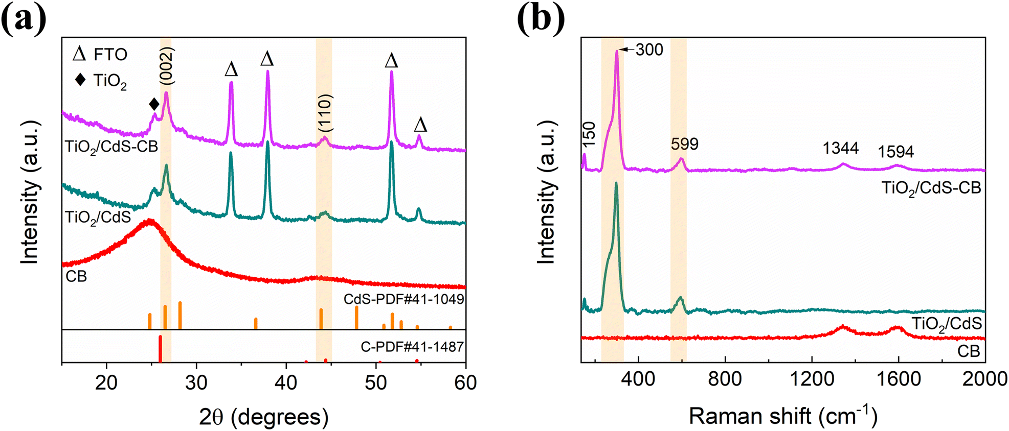 | ||
| Fig. 1 (a) XRD patterns and (b) Raman spectra of CdS and CdS–CB films. The respective analysis of CB powders is also included. The orange regions correspond to the peaks related to CdS. | ||
In addition, the XPS spectra in Fig. 2 demonstrate the successful deposition of the CdS–CB nanocomposite film onto TiO2. Fig. 2a shows the C 1s spectrum in CdS–CB film, in which the fitted peaks at 284.5, 286.2, and 289.1 eV are ascribed to sp2-hybridized carbon, carbonyl, and carboxyl functional groups, respectively.19,25 On the other hand, Fig. 2b and c exhibit the typical Cd 3d and S 2p spectra of both samples, respectively. For the TiO2/CdS sample, two characteristic peaks at 405.6 and 412.4 eV are associated with Cd 3d5/2 and Cd 3d3/2, respectively, whereas the peaks at 161.5 and 162.7 eV are assigned to S 2p3/2 and S 2p1/2, respectively.18 These values also confirm the Cd2+ and S2− oxidation states in CdS film.17 Compared with the TiO2/CdS sample, the Cd 3d and S 2p peaks of both spectra in the CdS–CB nanocomposite film (Fig. 2b and c) are downshifted by ∼0.8 eV. These downshifts are in accordance with previous nanocomposites based on chalcogenides and carbon nanostructures, such as CdS–carbon nanotubes18 and Sb2S3–graphene sheets,26 which have been attributed to an enhanced electron density around the chalcogenide, indicating electron transfer from carbon to CdS. These observations are in accordance with the increased n-type behavior of the CdS–CB nanocomposite found later in the work function results.
 | ||
| Fig. 2 (a) C 1s XPS spectrum of the CdS–CB nanocomposite film. (b) Cd 3d and (c) S 2p XPS spectra of the TiO2/CdS and TiO2/CdS–CB samples. | ||
The surface morphology and roughness characterization of the CdS–CB nanocomposite film were conducted by SEM and AFM. The cross-sectional SEM images (Fig. 3a and b) suggest that the thicknesses of CdS and CdS–CB layers deposited onto TiO2 are nearly similar, i.e., ∼96 and ∼101 nm for TiO2/CdS and TiO2/CdS–CB substrates, respectively. In Fig. 3c and d, the top view SEM images show that both samples are composed of small nanoparticles tightly integrated into a compact film. Interestingly, the boundaries between nanoparticles in the CdS–CB nanocomposite are better defined than those of the CdS film, providing a suitable nucleation surface for the subsequent Sb2S3 deposition. However, given that CB powder also consists of small nanoparticles (Fig. S3†), no visible differentiation between CdS and CB nanoparticles in the CdS–CB nanocomposite film can be observed. As shown in Fig. 3e and f, the AFM images corroborate that fine nanoparticles agglomerate to form large grains. Moreover, the CdS–CB layer exhibits a reduction in the root mean square surface roughness from 21.7 to 16.6 nm compared with the CdS layer.
 | ||
| Fig. 3 SEM images showing the: (a and b) cross-sectional and (c and d) top views of TiO2/CdS and TiO2/CdS–CB substrates. (e and f) Surface AFM images of both substrates. | ||
Fig. 4a shows the UV-visible (vis) transmittance spectra of the CdS and CdS–CB layers on TiO2. It can be observed that the transmittance curve of the substrate with CdS–CB is slightly improved compared to that of the pure CdS, especially with a 2.2% improvement in the range of 350–550 nm, increasing light availability for the Sb2S3 film. In addition, the characteristic transmittance edge of CdS can be identified in both spectra at ∼530 nm.27 The optical band gaps extracted from the Tauc plot (Fig. 4a inset) are found to be not significantly different between TiO2/CdS and TiO2/CdS–CB nanocomposite, with values of 2.37 and 2.36 eV, respectively. The electrical conductivity of the CdS and CdS–CB substrates was also determined from current–voltage curves, as shown in Fig. 4b. It is observed that the CdS film exhibits a lower slope than that of the CdS–CB, indicating a higher electrical conductivity in the nanocomposite film. The value of the electrical conductivity increases from 1.7 × 10⁻³ S cm−1 (CdS) to 21.3 × 10⁻³ S cm−1 (CdS–CB). Fig. 4c shows that the average work function of the TiO2/CdS is higher compared to that of TiO2/CdS–CB, which results in an n-type CdS–CB nanocomposite buffer layer. These findings reveal that the electronic interaction between CdS and CB nanoparticles impacts the optoelectronic properties of the hybrid nanocomposite layer.
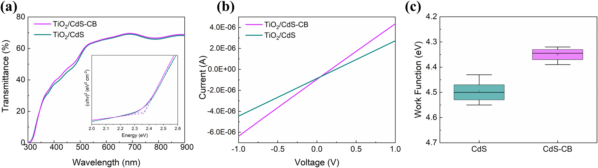 | ||
| Fig. 4 (a) UV-vis transmittance spectra, (b) current–voltage curves, and (c) average work functions of the TiO2/CdS and TiO2/CdS–CB substrates. Inset in (a) shows the Tauc plot. | ||
Sb2S3 films were hydrothermally grown onto the TiO2/CdS and TiO2/CdS–CB substrates, as detailed in the Experimental section. XRD, Raman, UV-vis absorption, and SEM measurements revealed no significant differences between both Sb2S3 films, as shown in Fig. S4 and S5.† Basically, the XRD and Raman peaks of the two Sb2S3 films can be indexed to the single crystal structure of stibnite (PDF#42-1393) with an optical band gap of ∼1.7 eV. Top-view SEM images of the Sb2S3 films reveal that the two layers are smooth without significant pinholes or defects. Then, interfacial charge transfer between Sb2S3 and TiO2/CdS and TiO2/CdS–CB substrates was conducted using SPV spectroscopy. Fig. 5a displays the SPV decays, in which the recombination lifetime at the substrate/Sb2S3 interface was estimated from a biexponential fit.28 It is found that the interfacial recombination lifetime for the TiO2/CdS–CB substrate is significantly lower than that of TiO2/CdS substrate, i.e., 43.1 and 62.6 s, respectively. Thus, although the structural and optical characterizations exhibit an almost unchanged crystal structure of Sb2S3 film after CB incorporation, a better charge transfer between the nanocomposite and Sb2S3 is observed.
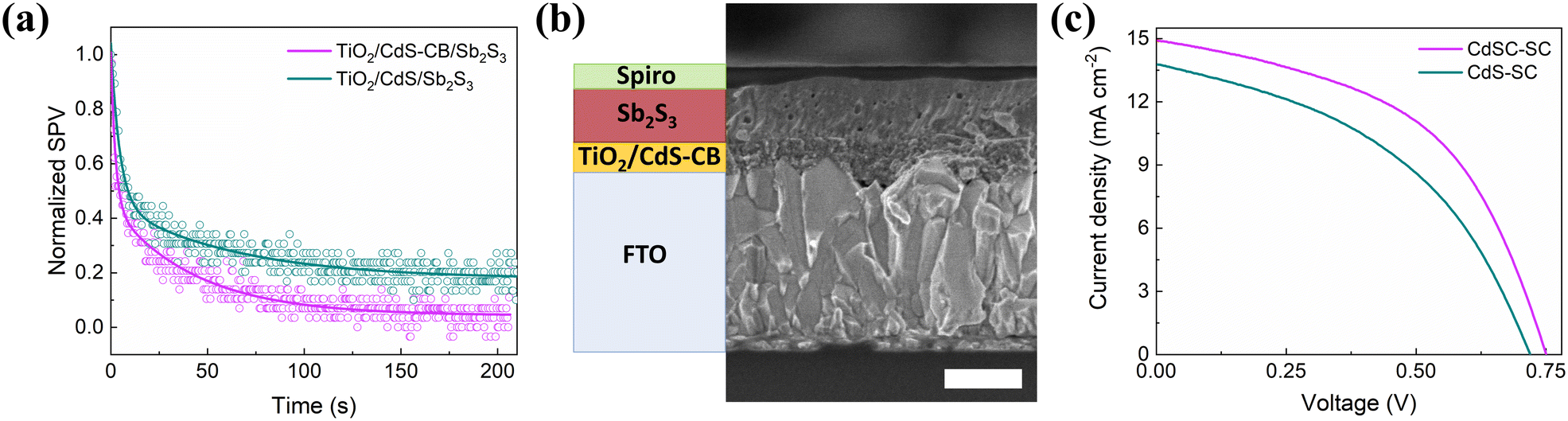 | ||
| Fig. 5 (a) SPV decays of Sb2S3 on TiO2/CdS and TiO2/CdS–CB substrates. (b) Cross-view SEM image of CdSC-SC. Inset bar: 200 nm. (c) J–V characteristics of the champion CdS-SC and CdSC-SC devices. | ||
Based on the aforementioned features involving the CdS–CB nanocomposite, Sb2S3 solar cells were fabricated to investigate its potential use as a buffer layer. Hereafter, the devices with CdS and CdS–CB buffer layers are denoted as CdS-SC and CdSC-SC, respectively. Fig. 5b shows a typical cross-view SEM image of CdSC-SC, indicating Sb2S3 and HTM films of 194 and 69 nm average thickness, respectively. It is worth noting that the best-performing solar cell based on the CdS–CB nanocomposite was reached using an optimized amount of 1.5 mg CB (Fig. S6 and Table S1†). The higher the amount of CB, the higher the short-circuit current density (Jsc). However, the 1.7 mg CB device has lower open-circuit voltage (Voc) and fill factor. As shown in Fig. 5c and Table 1, the CdSC-SC device exhibits a superior PCE compared with CdS-SC, mainly due to a significant enhancement in Jsc. This improvement is in agreement with the higher transport within the CdS–CB film and better charge transfer between Sb2S3 and the CdS–CB nanocomposite found in the electrical conductivity and SPV results, respectively. Fig. S7† compares the IPCE spectra of the CdS-SC and CdSC-SC devices, also indicating that the CdSC-SC shows a higher photoresponse over the entire wavelength range. The integrated Jsc obtained from the IPCE spectra (Fig. S7†) exhibits a similar trend with the Jsc values from J–V measurements, increasing from 13.03 to 14.19 mA cm−2. Additionally, the observed improvement in transmittance in the range of 350–550 nm causes a 1.1-fold enhancement in the photocurrent, i.e., 6.73 and 7.32 mA cm−2 for CdS-SC and CdSC-SC devices, respectively. Considering that no visible differences in structural, morphological, and optical properties of Sb2S3 deposited on the buffer layer with and without CB were found; the enhanced electronic density around CdS and the improved transmittance led to increased Jsc. Table S2† compares the photovoltaic parameters obtained in this work with those of hydrothermally processed Sb2S3 solar cells using TiO2 and TiO2/CdS as buffer layers.
| Device | J sc (mA cm−2) | V oc (V) | Fill factor (%) | PCE (%) |
|---|---|---|---|---|
| CdSC-SC | 14.54 ± 0.28 (14.92) | 0.73 ± 0.02 (0.75) | 53.31 ± 0.41 (53.81) | 5.7 ± 0.23 (6.03) |
| CdS-SC | 13.27 ± 0.36 (13.74) | 0.7 ± 0.02 (0.72) | 49.58 ± 0.55 (50.03) | 4.62 ± 0.27 (4.95) |
To obtain further understanding of how the nanocomposite buffer layer enhances the photovoltaic performance of the CdSC-SC device, dark J–V analysis was implemented. From Fig. 6a, it is observed that the CdSC-SC device exhibits a lower reverse saturation current (J0) than that of the CdS-SC device, which is reduced from 7.78 × 10⁻¹⁰ to 4.61 × 10⁻⁸ mA cm−2. According to this analysis,29 a lower J0 implies a better junction quality at the buffer layer/Sb2S3 interface, reducing the leakage current and improving the Voc and fill factor in the CdSC-SC devices. This finding agrees well with the photovoltaic performance (Fig. 5c). Additionally, Fig. 6b displays the dependency of Voc on the light intensity (I) range (10–100 mW cm−2) of the devices. The ideality factor (n) was obtained from the slope of the fitted line using the expression: Voc = nkT/e·ln(I) + constant, where k, T, and e refer to the Boltzmann constant, absolute temperature, and elementary charge, respectively. The n values are found to be 1.57 and 1.74 for the CdSC-SC and CdS-SC devices. As the n values are between 1 and 2, both devices present monomolecular and bimolecular trap-assisted recombination.30 However, the use of the nanocomposite buffer layer is beneficial in reducing the trap states at the buffer layer/Sb2S3 interface. This reduction can be explained by the effective interaction between CB and CdS in the nanocomposite film, which decreases the roughness of the buffer layer and the trap state recombination.
 | ||
| Fig. 6 (a) Dark J–V curves, (b) Voc as a function of light intensity, and (c) Nyquist plots of CdSC-SC and CdS-SC devices. The inset of (c) shows a zoom-in of the high-frequency region. | ||
Furthermore, EIS measurements were conducted to assess the influence of using the CdS–CB nanocomposite buffer layer on the charge transport mechanism within solar cells. Fig. 6c shows the Nyquist plots for the CdS-SC and CdSC-SC devices recorded near the Voc value in each case. The fitted data using the equivalent circuit (Fig. S8†) allows the extraction of important parameters such as the series resistance (Rs) and recombination resistance (Rrec). As expected, the CdSC-SC device has lower Rs (15.97 Ω) and higher Rrec (2256.74 Ω) than the CdS-SC device (Rs = 19.01 Ω and Rrec = 435.67 Ω). The results indicate that incorporating CB into the CdS layer causes fewer trap states, facilitating charge transport with less recombination. These findings are represented in the energy level diagram of the two buffer layers in Fig. S9.†
4. Conclusions
In summary, we developed an efficient hybrid nanocomposite film consisting of CdS and carbon black nanoparticles prepared by a one-step chemical bath deposition method for application as a buffer layer in Sb2S3 solar cells. It is found that the CdS–CB nanocomposite film deposited on TiO2 exhibits higher electrical conductivity, more n-type nature and lower roughness compared to that of pristine CdS film. After the optimal concentration of CB was adjusted, the champion solar cells fabricated with the CdS–CB yielded a PCE of 6.03%. Furthermore, the CdS–CB hybrid nanocomposite buffer layer improves the junction quality at the buffer layer/Sb2S3 interface, reducing the trap states recombination. Thus, this work is expected to highlight using a CdS buffer layer in solar cells without further post-treatment.Author contributions
R. E. Castellanos-Pineda: investigation, data curation, validation, writing – original draft, and visualization. A. Baron-Jaimes: investigation, data curation, and validation. M. A. Millán-Franco: investigation, data curation, and validation. M. E. Rincón: project administration, funding acquisition, and writing – review & editing. O. A. Jaramillo-Quintero: conceptualization, data curation, project administration, funding acquisition, supervision, writing – original draft, and writing – review & editing.Conflicts of interest
There are no conflicts to declare.Acknowledgements
This work was financially supported by Universidad Nacional Autónoma de México (PAPIIT-IN111722). R. E. Castellanos-Pineda and A. Baron-Jaimes would like to acknowledge the fellowships provided by CONACYT-México. We are thankful for the technical assistance by E. Barrios-Salgado, R. Morán Elvira, M. L. Ramón and J. Campos.References
- J. Mangum, S. Theingi, M. Steiner, W. McMahon and E. Warren, Cryst. Growth Des., 2021, 21, 5955–5960 CrossRef CAS.
- W. K. Metzger, S. Grover, D. Lu, E. Colegrove, J. Moseley, C. L. Perkins, X. Li, R. Mallick, W. Zhang, R. Malik, J. Kephart, C.-S. Jiang, D. Kuciauskas, D. S. Albin, M. M. Al-Jassim, G. Xiong and M. Gloeckler, Nat. Energy, 2019, 4, 837–845 CrossRef CAS.
- X. Chang, J. Chen, S. Ma, B. Chen, X. Zhang, Q. Gao, F. Li, J. Wang, D. Song and J. Chen, Adv. Mater. Interfaces, 2023, 10, 2202171 CrossRef CAS.
- M. A. Farhana, A. Manjceevan and J. Bandara, J. Sci.: Adv. Mater. Devices, 2023, 8, 100533 CAS.
- C. Chen, K. Li and J. Tang, Sol. RRL, 2022, 6, 2200094 CrossRef CAS.
- J. Li, Z. Gao, X. Hu, S. Wang, Y. Liu, C. Wang, K. Dong, Z. Zeng, C. Tao and G. Fang, Adv. Funct. Mater., 2023, 33, 2211657 CrossRef CAS.
- I. Sharma, P. S. Pawar, R. K. Yadav, R. Nandi and J. Heo, Sol. Energy, 2022, 246, 152–180 CrossRef CAS.
- Y. C. Choi, D. U. Lee, J. H. Noh, E. K. Kim and S. Il Seok, Adv. Funct. Mater., 2014, 24, 3587–3592 CrossRef CAS.
- S. Wang, Y. Zhao, B. Che, C. Li, X. Chen, R. Tang, J. Gong, X. Wang, G. Chen, T. Chen, J. Li and X. Xiao, Adv. Mater., 2022, 34, 2206242 CrossRef CAS PubMed.
- X. Jin, Y. Fang, T. Salim, M. Feng, S. Hadke, S. W. Leow, T. C. Sum and L. H. Wong, Adv. Funct. Mater., 2020, 30, 2002887 CrossRef CAS.
- L. Zhang, W. Lian, X. Zhao, Y. Yin, T. Chen and C. Zhu, ACS Appl. Energy Mater., 2020, 3, 12417–12422 CrossRef CAS.
- F. You, S. Chen, T. Ma, F. Xiao, C. Chen, H.-Y. Hsu, H. Song and J. Tang, Energy Technol., 2022, 10, 2200940 CrossRef CAS.
- O. A. Jaramillo-Quintero, M. E. Rincón, G. Vásquez-García and P. K. Nair, Progr. Photovolt.: Res. Appl., 2018, 26, 709–717 CrossRef CAS.
- Z. Chen and G. Chen, Sol. Energy, 2020, 201, 323–329 CrossRef CAS.
- Z. Feng, S. Sun, Y. Sun, X. Liu, H. Liu and H. Liu, Appl. Phys. A: Mater. Sci. Process., 2021, 128, 479 CrossRef.
- Y. Zhao, S. Wang, C. Jiang, C. Li, P. Xiao, R. Tang, J. Gong, G. Chen, T. Chen, J. Li and X. Xiao, Adv. Energy Mater., 2021, 12, 2103015 CrossRef.
- J. Li, Y. Zhao, C. Li, S. Wang, X. Chen, J. Gong, X. Wang and X. Xiao, Adv. Sci., 2022, 9, 2202356 CrossRef CAS PubMed.
- Y. V. Fedoseeva, L. G. Bulusheva, I. P. Asanov, A. G. Kurenya, A. V. Gusel'nikov, E. A. Maksimovskiy, D. V. Gulyaev, K. S. Zhuravlev, A. K. Gutakovskii and A. V. Okotrub, Synth. Met., 2021, 273, 116671 CrossRef CAS.
- Z. Zhu, Y. Han, C. Chen, Z. Ding, J. Long and Y. Hou, ChemCatChem, 2018, 10, 1627–1634 CrossRef CAS.
- C. Zhu, C. Liu, Y. Zhou, Y. Fu, S. Guo, H. Li, S. Zhao, H. Huang, Y. Liu and Z. Kang, Appl. Catal., B, 2017, 216, 114–121 CrossRef CAS.
- L. Sheeney-Haj-Ichia, B. Basnar and I. Willner, Angew. Chem., Int. Ed., 2004, 44, 78–83 CrossRef PubMed.
- V. M. Dzhagan, M. Y. Valakh, C. Himcinschi, A. G. Milekhin, D. Solonenko, N. A. Yeryukov, O. E. Raevskaya, O. L. Stroyuk and D. R. T. Zahn, J. Phys. Chem. C, 2014, 118, 19492–19497 CrossRef CAS.
- M. F. Saleem, H. Zhang, Y. Deng and D. Wang, J. Raman Spectrosc., 2016, 48, 224–229 CrossRef.
- O. A. Jaramillo-Quintero, R. V. Barrera-Peralta, A. Baron-Jaimes, R. A. Miranda-Gamboa and M. E. Rincón, RSC Adv., 2021, 11, 31566–31571 RSC.
- B. Gupta, N. Kumar, K. Panda, V. Kanan, S. Joshi and I. Visoly-Fisher, Sci. Rep., 2017, 7, 45030 CrossRef CAS PubMed.
- X. Xiong, G. Wang, Y. Lin, Y. Wang, X. Ou, F. Zheng, C. Yang, J.-H. Wang and M. Liu, ACS Nano, 2016, 10, 10953–10959 CrossRef CAS PubMed.
- B. Liu, R. Luo, Q. Liang, Y. Zheng, B. Li, J. Zhang, W. Li, L. Wu and L. Feng, J. Mater. Sci.: Mater. Electron., 2015, 26, 9985–9990 CrossRef CAS.
- O. A. Jaramillo-Quintero, Y. A. Alarcón-Altamirano, R. A. Miranda-Gamboa and M. E. Rincón, Appl. Surf. Sci., 2020, 526, 146705 CrossRef CAS.
- Y. Mao, Y.-H. Hu, X.-Y. Hu, L.-Q. Yao, H. Li, L.-M. Lin, P. Tang, H. Li, S. Chen, J.-M. Li and G.-L. Chen, Adv. Funct. Mater., 2022, 32, 2208409 CrossRef CAS.
- D. A. Kara, E. K. Burnett, K. Kara, O. Usluer, B. P. Cherniawski, E. J. Barron, B. Gultekin, M. Kus and A. L. Briseno, Phys. Chem. Chem. Phys., 2022, 24, 10869–10876 RSC.
Footnote |
| † Electronic supplementary information (ESI) available. See DOI: https://doi.org/10.1039/d3lf00235g |
| This journal is © The Royal Society of Chemistry 2024 |