
 Open Access Article
 This Open Access Article is licensed under a
 Creative Commons Attribution 3.0 Unported Licence
Nanofluidic resistive pulse sensing for characterization of extracellular vesicles†
Madalena R. C.
Calado
a,
Teresa C.
Lage
a,
Daniel A. M.
André
a,
Carlos
Calaza
a,
Carlos
Marques
a,
Carolina
Herrero
bc,
João
Piteira
a,
Lars
Montelius‡
a,
Dmitri Y.
Petrovykh
 a,
Lorena
Diéguez
*a and
Alar
Ainla
*a
a,
Lorena
Diéguez
*a and
Alar
Ainla
*a
aInternational Iberian Nanotechnology Laboratory (INL), Braga, Portugal. E-mail: lorena.dieguez@inl.int; alar.ainla@inl.int
bTranslational Medical Oncology Group (Oncomet), Health Research Institute of Santiago de Compostela (IDIS), University Hospital of Santiago de Compostela (SERGAS), Santiago de Compostela, Spain
cNasasbiotech, S.L., A Coruña, Spain
First published on 25th July 2024
Abstract
This paper describes the development, design and characterization of a resistive pulse sensing (RPS) system for the analysis of size distributions of extracellular vesicles (EVs). The system is based on microfluidic chips fabricated using soft-lithography and operated in pressure-driven mode. This fabrication approach provided reproducible pore dimensions and the best performing chip design enabled, without calibration, sizing of both 252 nm and 460 nm test particles within 8% of theoretically calculated values, based on the size specifications provided by suppliers. The number concentration measurement had higher variations and without calibration provided estimates within an order of magnitude, for sample concentrations across 4 orders of magnitude. The RPS chips could also measure successfully EVs and other biological nanoparticles in purified samples from cell culture media and human serum. A compact, fast and inexpensive RPS system based on this design could be an attractive alternative to current gold-standard techniques for routine characterization of EV samples.
Tribute to George WhitesidesThe breadth of experience I gained in Whitesides' group would require a book to fully describe and far exceeded even my wildest prior imaginations. It could be titled “Complexity and Simplicity.” While also the name of a research theme in the group at the time, the search for simplicity within the complexities of the world was a deeper underlying philosophy in nearly everything we did. The spirit of the lab combined playful creativity, almost artistic exploration of often unusual ideas across seemingly distant scientific fields—from chemistry to robotics—with highly structured thinking guided by his “outline method”.Although a pioneer of many fields, he never stopped asking us what the next “big thing” could be. This quest also taught me about the humanistic nature of science and the profound importance of simplicity in creating understanding and inspiration. Training involved many drafts of every manuscript, on which he gave handwritten feedback on every detail. Some of these approaches I now use and teach to my students. Besides being a truly inspirational mentor himself, I must mention the importance of the group he created and the fellow colleagues who became lasting friends. Thank you, George! – Alar Ainla, Whitesides Group alumni, 2014–2017. |
Introduction
Extracellular vesicles (EVs) are small (30 nm to 1 μm) lipid vesicles released by many cell types in the body.1,2 The overall challenge of EV isolation and characterization stems from their wide size range as well as their sizes and densities overlapping with those of more abundant lipoproteins, thereby complicating both density-based and size-based separation methods.3 Among other techniques that are used for measuring EVs, resistive pulse sensing (RPS) implemented via microfluidic chips offers a promising combination of beneficial characteristics.The size distribution and concentration of EVs are important parameters to be determined in most research and clinical analysis protocols4 because, for example, EV samples obtained using different isolation methods can vary considerably in terms of their size distributions and mean diameter.5 For example, a study by Brennan et al.6 demonstrated significant differences between size distribution, modal size and concentration depending on the isolation method or their combinations, with maximum size difference of a factor of three and concentration difference of three orders of magnitude.
Currently the most common methods for analyzing size and concentration of EVs are dynamic light scattering (DLS), nanoparticle tracking analysis (NTA), and nano flow-cytometry (nFC). DLS is a common method, due to relative ease of use, particularly on commercial instruments that typically can assess very large size range of particles (from sub-nm till about 10 μm) and particle concentrations. Size measurements using DLS, however, are reliable only for narrowly dispersed samples: the scattered light is proportional to the 6th power of the particle size, so even a small fraction of larger particles can overwhelm the DLS signal and distort the outcome. NTA is another popular technique that, in contrast to the ensemble measurements by DLS, measures single particles by monitoring their Brownian motion in a flow-cell using optical microscopy. It can characterize particles in the size range from 30 nm to 1 μm. While NTA can measure concentration and handles polydisperse samples well, it can be practically applied only to samples within a narrow concentration range. In fact, too low concentrations result in low number of data points and too high hinders tracking of particles due to the overlap of their paths. A variant of fluorescent cytometry specifically optimized for nanoparticle analysis is nFC, which uses scattered and fluorescent light to characterize particles passing through a laser beam; nFC can measure particles in the range of about sub 10 nm to 1 μm at a rate of 100 s of particles per second, as well as characterize their concentration. Both NTA and nFC rely on precision optics, making them difficult to implement in miniature and low-cost systems.
Methods for characterization of EVs that rely on large, advanced instruments include transmission electron microscopy (TEM) and centrifugal liquid sedimentation (CLS). TEM offers a unique option for morphological studies of EVs and very high size resolution, but only for a limited number of EVs at a time. CLS characterizes nanoparticles by monitoring the time evolution of their distribution through fluid medium, while spinning in the centrifuge, providing information about size (Stokes' radius) and density. It can measure particles in the range of about 20 nm to 10 μm, with sample concentrations typically below 0.2% (v/v). CLS can offer size resolution of about 5%, but quantitative characterization of distributions requires complex models and calibrations, due to the interplay of various parameters, such as density and extinction.
RPS holds a promise to overcome some of challenges associated with the other techniques briefly discussed above and compared in Fig. 1(A). RPS is based on temporary blocking of ionic current through a small pore by particles passing through it. Similar to nFC, particles are measured one-by-one, providing detailed information about them. In contrast to nFC, NTA, and DLS, the RPS measurements are fully electronic and do not involve optical components, opening opportunities for miniaturization and lowering the cost of the measurement systems.
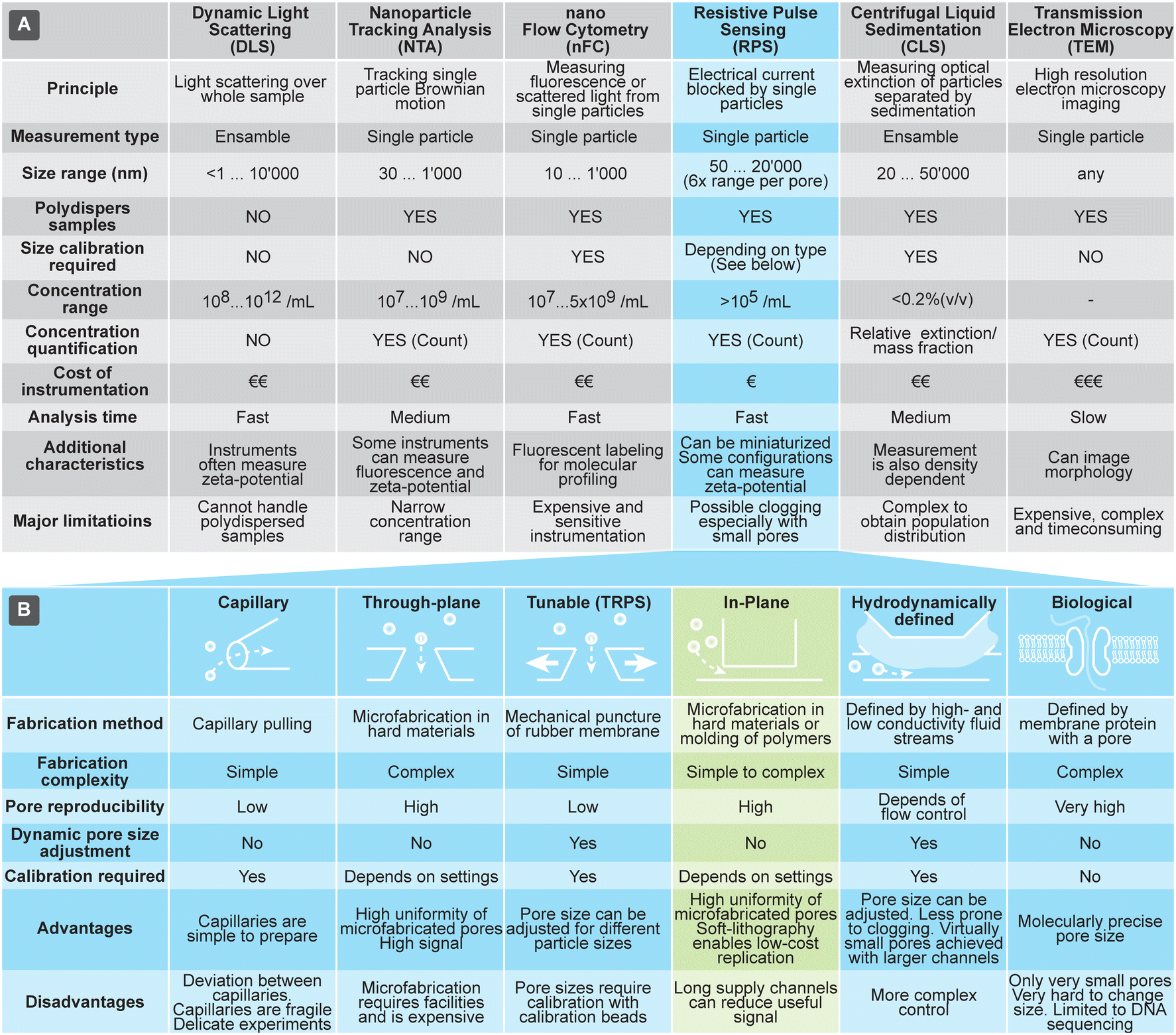 | ||
| Fig. 1 (A) Overview of techniques used for characterization of extracellular vesicles (EVs). (B) Comparison of different approaches to implement resistive pulse sensing (RPS). | ||
The history of RPS dates back as far as 1940s, when Wallace Coulter developed and patented an electrical counting device for blood cells.7 In 1970s the miniaturization of the same principle reached sub-micron particles8 and in 1990s devices integrating biological nanopore protein α-haemolysin were able to measure even molecules, enabling applications in DNA sequencing.9
In all variants of RPS the current is partially blocked by the particle passing a pore, resulting in a small current drop ΔI (a spike). The relative spike (ΔI/I) is roughly proportional to the volume of the particle.10 However, it should be noted that definition of the particle size for RPS, DLS, NTA and TEM is not identical, due to the different physical measurement principle. While DLS and NTA determine hydrodynamic radius of the particles, RPS measures exclusion of ionic current and TEM geometrical shape. In case of biological particles, these can differ due to the hydration shell and protein corona.11 In RPS the maximum measurable particle size is defined by the pore size, while the minimum measurable size is defined by the electronic noise, which limits the detection of small spikes. Practical ratio between maximum and minimum diameter depends on implementation but could be as high as around 6-fold for a single fixed-size pore.
The RPS detection principle can be implemented in a variety of ways, using pores with either fixed geometries, adjustable dimension, or virtual boundaries. Fig. 1B compares different approaches to prepare measurement pores for RPS. One of the simplest methods to prepare fixed-size pores is by using a capillary puller used in electrophysiology and cell biology. Capillary orifices with dimeter <50 nm can measure, for example, particles smaller than 10 nm.12,13 More robust and consistent pores than in pulled capillaries can be achieved using microfabrication, where approaches are broadly divided into i) “through-plane” pores, which are small holes etched through a thin layer of material14,15 or ii) “in-plane” pores, which are small constrictions or nano-channels inside of microfluidic devices.
In-plane pore designs are versatile and possible to implement in a variety of materials: they can be etched into hard materials16 or molded into polymers using soft-lithography.17,18 Complex pore structures, such as series of constrictions, are also possible.16 Furthermore, the in-plane approach offers the possibility for rapid and low-cost prototyping of RPS devices in laboratory settings by using soft-lithography.
To overcome typical challenges of the RPS related to the calibration requirements and possible pore clogging, we present a nanoparticle characterization system and evaluate its performance. Specifically, we demonstrate a simple in-plane microfluidic device design (Fig. 2) with easy, fast and low-cost laboratory replication using soft-lithography,19 where only the initial master mold was prepared in a specialized micro- and nanofabrication facility. We have systematically studied relations between different nanopore geometries, test particle sizes, buffer conductivity and operational settings, to optimize success rate and accuracy of the measurements, to be able to obtain particle-size distributions even without calibration. Finally, we demonstrated that this system could measure biological nanoparticles in a sample of purified EVs and directly in human serum.
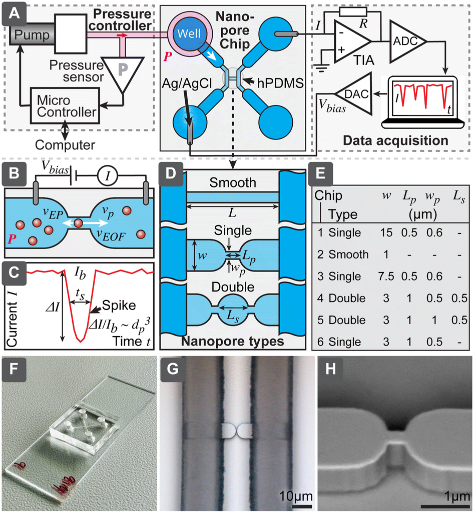 | ||
| Fig. 2 Resistive pulse sensing platform presented in this paper. (A) System containing nanopore chip, electronic readout based on patch-clamp amplifier or home-built electronics and pressure controller. (B) Principle of nanopore chip and (C) correspondingly obtained electronic signal corresponding to a particle. (D) Types of nanopores and (E) dimensions of six nanopore designs evaluated here. (F) Photograph of a PDMS nanopore chip bonded to a microscopy slide. (G) Optical microscopy and (H) SEM image of the master used to mold nanopores. | ||
Materials and methods
Nanopore chip
Nanopore chips were designed in AutoCAD (Autodesk Inc. San Francisco, CA). All six evaluated nanopore geometries (chip 1–6 in the text refers to the chip types according to Fig. 2) were included in the same master layout and fabricated on a single wafer. ESI† lists the detailed fabrication process and device geometries. Briefly, we fabricated the master mold as following: nanopore structures were patterned using electron beam lithography and etched into 1 μm-thick silicon dioxide, supporting microfluidics contained micro- and macro channels with heights of 15 μm and 95 μm, respectively. These channels were fabricated using optical lithography and the negative photoresist SU8. The final master was used for soft-lithographic replication of nanopore chips. Two formulations of polydimethylsiloxane (PDMS) elastomers were used for the chip: the area close to the nanopores was fabricated from harder PDMS (hPDMS) composed of 1![[thin space (1/6-em)]](https://www.rsc.org/images/entities/char_2009.gif) :1 mixture of GELEST® hPDMS and Sylgard 184, while remainder of the device body was fabricated from softer PDMS (Sylgard 184). After curing the PDMS, 3 mm wells were punched for the liquid storage and devices were plasma-bonded to a standard glass slide. Final devices were loaded with 0.1% water solution of Pluronic F-127 and stored until used.
:1 mixture of GELEST® hPDMS and Sylgard 184, while remainder of the device body was fabricated from softer PDMS (Sylgard 184). After curing the PDMS, 3 mm wells were punched for the liquid storage and devices were plasma-bonded to a standard glass slide. Final devices were loaded with 0.1% water solution of Pluronic F-127 and stored until used.
RPS system
RPS system contained a miniature computer-controlled pressure generator, which allowed to set pneumatic pressure (P) in the range 0 to 500 mbar with uncertainty and stability within ±5 mbar. In order to drive the fluid flow, pressure was applied to the input well using a small insert based on a luer-lock adapter. For electrical interfacing, Ag/AgCl electrodes were prepared from Ag wires and inserted into the wells on the opposite side of the pore. Readout was based on trans-impedance amplifiers. For most experiments a commercial patch-clamp amplifier MultiClamp 700B (Molecular Devices) coupled with signal digitizer Digidata 1440A (Molecular Devices) was used. Bias voltage (Vbias) was set to 30 or 100 mV and amplifier gain (RG) to 40 MΩ, giving a full current range ±125 nA. Signal was recorded with a 20 kHz sampling rate. In order to reduce noise, the system was shielded using a Faraday cage.We also constructed a home-built low-cost miniaturized readout system and evaluated its performance for RPS sensing (further details are described in ESI† Section S6). For data processing we developed an automated data analysis software using MATLAB R2018b (MathWorks Inc. Natick, MA), described in ESI† Section S4.
Evaluation
Evaluations were performed in two electrolyte buffers based on phosphate buffered saline (PBS) prepared from powder concentrate with 81% NaCl (Fisher Bioreagents BP661-10). Low-salt (LS) and high-salt (HS) buffers had NaCl concentrations of 137 mM and 1 M and conductivities of σ = 1.46 S m−1 and σ = 3.45 S m−1, respectively. For test particles we used three different polystyrene beads: 460 nm F8812 (Invitrogen, Waltham, MA), 252 nm PS-R-KM239 (microParticles GmbH, Berlin, Germany) and 230 nm custom-made.20 Particle solutions had the following characteristics: F8812 (supplier's specifications: size 460 ± 27 nm, carboxylated surface, density 1.055 g cm−3, concentration 2% solid content, ca. 2.9 × 10¹¹ particles per mL), PS-R-KM239 (supplier's specifications: size 252 ± 6 nm, concentration 5% solid content, ca. 5.7 × 10¹² particles per mL), custom-made (size: ∼230 nm, concentration: ∼2.5 × 10¹² particles per mL). Particle stock solutions were serial diluted in steps of 10× in the range 100× to 100000× (final concentrations: 0.001%, 0.01%, 0.1% and 1% of stock). A small amount (ca. 10–20 μL) of test solution and clean buffer of corresponding salt-concentration were introduced to the wells on the opposite sides of the pores. Then chips were fitted with pressure adapters and Ag/AgCl electrodes and measurements were performed at different pressures and bias voltages. For comparison purposes, samples were also characterized by conventional NTA NanoSight NS300 and DLS Zetasizer Nano, both from Malvern Instruments (Malvern, UK) (ESI† Section S9.2).
Examples of biological samples
For evaluation with biological samples, we used three different samples: two purified EVs samples from the supernatant of HCT116 and HEC-1A cell lines and human serum (H4522-20ML, Sigma-Aldrich, Merck). Preparation21 and characterization of EVs samples is described in detail in ESI† Section S8.Results and discussion
Design of the system
While RPS has been studied extensively, the aim of our work has been to develop and optimize a low-cost RPS system that would be simple and robust to fabricate and to operate and that eventually could become the basis for a small, cost-effective instrument, useful for the routine characterization of EV samples, complementing current standard techniques, such as NTA and DLS. This system would include i) a nanopore chip, where the detection takes place, ii) control and readout mechanism to drive the flow and register signals from the chip, iii) software to process the measured signals and present the results and iv) protocols for operation (Fig. 2A). The technology we present here encompasses all these aspects. Since the key significance for practical usefulness of the technique is robustness, we have compared 6 different pore geometries with different width, length and number of constrictions, shown in Fig. 2D and E. We have also tested different ionic strengths and evaluated how all the above-mentioned parameters would affect the yield of successful measurements for different test particles. Afterwards, best performing designs were chosen for further detailed evaluation, to understand their accuracy for calibration-free particle sizing and concentration measurements and biological tests.Nanopore chip
Is a fluidic device with micro- and nanochannels, where the particle sample is loaded and detection takes place. The main element of the chip is the nanopore, which shall be slightly larger than the largest particle it is intended to detect, such that passing particles would cause maximum blockage of the ionic current, while still not clogging the pore (Fig. 2B). The ionic current is driven by the electric field from external electronics and requires electrodes to convert electronic current in wires to ionic current in electrolytes. To maximize the useful spiking signal (Fig. 2C), electrical resistivity of all parts of the circuitry, other than the nanopore, should be minimized.While several approaches to form the nanopores exist (Fig. 1B), we chose the in-plane type of structure, which allows for easy and fast replication of devices using molding (soft-lithography). Even though master molds are still needed and are produced using advanced microfabrication in a cleanroom facility, these masters can be used repeatedly. For example, all the devices used in this work were fabricated using a single 200 mm silicon wafer, producing 32 chips in one molding cycle. We included in the wafer 6 different geometries with a long smooth channel as well as with single and double constrictions (Fig. 2D and E), in order to study the effects of the geometry on the system performance.
All the silicone molding was performed in the standard laboratory environment, requiring only a balance, vacuum desiccator, oven, small cutting tools, and plasma cleaner, making the fabrication of the chip accessible, fast, and cost-effective in different laboratory settings. Only a minute amount of sample is needed for the analysis (maximum flow rate was below 80 nL s−1), therefore, to simplify interfacing as well as to minimize dead-volumes and resistance from long interconnects, wells to store the samples (10–20 μL) and supporting electrolytes were directly integrated into the chips.
Our chip structure contained two channel loops, which were connected by the nanochannel in the center (Fig. 1A and S1†); the purpose of the loops is to facilitate both the initial channel loading and the subsequent solution exchange. For example, nanochannels in the designs presented here have fluidic resistances about 230 to 1800× higher than do supply channels (Table S2†). With flow rates in the range 0.05 to 0.4 nL s−1 it would mean that replacing sample in the channel may take 1 h, while using loops with larger dimensions allows solution exchange in less than 15 s. Supply channels also had to be optimized in terms of their electrical resistance, while considering: i) practical spacing of wells, ii) mechanical stability of PDMS channels (channel cannot be too wide not to collapse) and iii) fabrication limitations of SU-8 (gap between two channels cannot be too deep). Therefore, we needed to divide supply channels into lower micro- and higher macrochannels (Fig. S1, Table S1†). Even though adding an additional lithography step to the fabrication of the master, this allowed us to reduce electrical resistance to less than 25% of the total resistance.
The fabrication process also required optimization after the use of the typical softer Sylgard 184 (sPDMS, elastic modulus ca. 2 MPa) resulted in collapse of the nanopores. Inspired by previous studies,22 we applied hard PDMS (hPDMS, elastic modulus ca. 9 MPa) around the nanochannels. However, when used neat, even small areas of hPDMS proved to be brittle and cracked frequently during the release from the mold, resulting in low yield of chips and faulty pores. Therefore, we optimized the elasticity of elastomer by mixing sPDMS and hPDMS, where 1:1 ratio provided the best performance, avoiding both collapse and cracking.
The final step to optimize was the chip functionalization. When stored dry, PDMS surfaces turn hydrophobic, making filling of small pores complicated, resulting in trapped air bubbles and absorption of particles on channel walls. This could be effectively avoided when we primed chips with the water solution of Pluronic F-127 (0.1% w/v) before storage inside a humidified zip-lock bag or a box.
Driving particles through the pores
Particle mobility through the pores could be driven by two mechanisms: electrical and hydraulic. Electrical mechanism relies on the electroosmotic flow (EOF) of liquid in the channels and the electrophoretic mobility (EF) of the particles, when electric field is applied. Hydraulic flow, on the other hand, is driven by applied pressure between the channel ends. We have described detailed analysis of both mechanism and their role in ESI† Section S2. Briefly, in case of the channels and particles used here, the EOF and EF are similar in the order of magnitude, around 1−2 × 10⁻⁸ m2 V−1 s−1, but in opposite direction; EOF would be in the range from 0.02 to 0.26 mm s−1 (Table S3†). The mobility, however, is dependent on the surface charges (zeta-potential) of channels and particles, which is further dependent on pH. In contrast, the pressure-driven hydraulic mechanism is independent of surface charges. In our typical operational settings, it should produce flow velocity in the pore in the range 12–150 mm s−1, which is about 500× faster, than electrical contribution.Pressure-driven RPS operation
In pressure-driven flow, we can neglect the electrical and chemical effects and obtained results should depend only on the particle size. In this case we would expect linear dependence between the flow velocity and applied pressure, which would be reflected both in the spike duration as well as in spiking frequency. This behaviour was confirmed as shown in Fig. 3: pressure variation between 50 and 150 mbar (Fig. 3A) resulted in negligible effect on the spike amplitudes (Fig. 3B), while velocity, measured as pore length L divided by pulse duration ts(L/ts), increased significantly (Fig. 3C). Velocity followed the linear slope of 0.1543 ± 0.0065 mm s−1 per mbar, which is close to the theoretically expected value of 0.12 mm s−1 per mbar (Table S3†). Spiking frequency also followed a linear dependence on the pressure (Fig. 3D), with the slope of 0.03248 ± 0.00038 Hz per mbar. Using relation c = 2RF_P·f/p gave us the theoretically expected number concentration 2.8 × 10⁸ mL−1, which agrees well with the diluted solution of nominally 2.9 × 10⁸ mL−1. While average frequency of spiking is proportional to the pressure and the particle concentration, the individual spikes are independent events governed by the Poisson process, where the distribution P of the delays between the individual spikes decays exponentially with the delay t: P{t} ∝ e−at (Fig. S7†). The disadvantage of the pressure-driven flow is the need for the pressure controller, which nevertheless can be constructed cost-effectively as described below.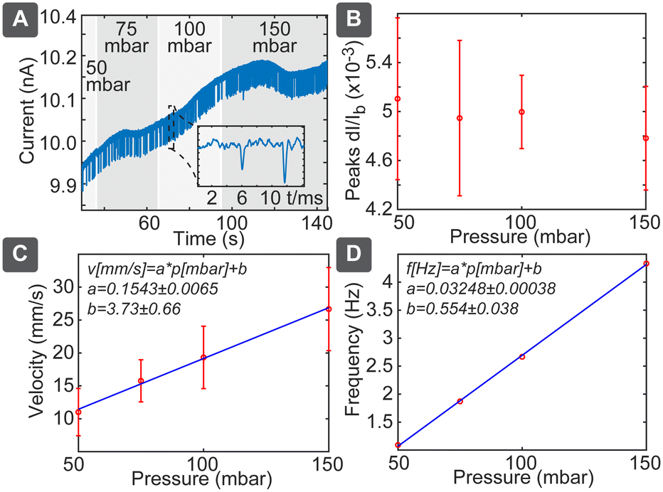 | ||
| Fig. 3 Pressure-driven RPS measurement. (A) Recording of raw signal with chip 2 at different applied pressures. Dependence of the (B) peak amplitude, (C) particle velocity and (D) spiking frequency on the applied pressure. | ||
Particle sizing
One of the most important capabilities of the RPS instrument is the ability to accurately determine the particle sizes. Determining the sizing accuracy itself would require the use of reference particles with well-defined dimensions, ideally a standard reference material. Establishing absolute dimensions of nanomaterials, however, has proven to be challenging. Metrological studies have found, that measured values could depend considerably (variation over 10%) on both the test lab and, even more significantly, the method used, such as different microscopy techniques, mobility analysis, DLS or X-ray scattering, in part, because they probe different physical characteristics.23 For the evaluation purposes here, we have used particle sizes reported by the suppliers. For side-by-side comparison we further measured and compared samples with standard techniques of NTA and DLS using commercial instruments (ESI† Section S9.2).Particles are sized individually based on the spike amplitude they produce when passing the pore. The spike amplitude is primarily determined by the particle volume and the cross-sectional area of the pore.10 The approximate particle dimeter dp can be expressed using eqn (1).
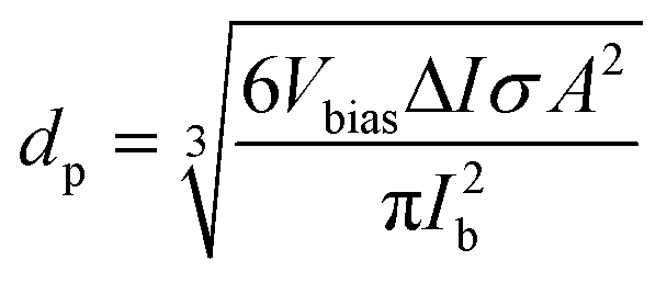 | (1) |
When we applied this model to our measured data, very good agreement with the particle sizes specified by the suppliers was generally achieved, even without calibration (Fig. 4). Chip 1 was tested for smaller particles, which produced a size distribution of 210 ± 29 nm (where ± is indicating standard deviation) vs. the nominal specification of 252 ± 6 nm, corresponding to a 20% lower mean and a nearly 5-fold broader distribution. In parallel, 252 nm particles measured 242 ± 40 nm in NTA and 280 ± 34 nm in DLS, when optimal dilutions were used, as values obtained with these standard techniques depended on the concentration (ESI† Section S9.2). Chip 3 provided for large particles the sizing of 470 ± 115 nm, consistent with the nominal specification of 460 ± 27 nm, but with a significantly increased distribution width, which could be due to the particle size being too close to the pore dimensions. Same particles measured slightly smaller 449.3 ± 93.5 nm in NTA and similarly 470 ± 40 nm in DLS. Thus, in both cases the NTA value being slightly smaller (<4%) and DLS larger (<12%) compared to the nominal specification. The same chip slightly overestimated (249.5 ± 6.2 nm) the size of the small 230 nm particles. Chip 5 had in our tests the poorest sizing performance, significantly underestimating the nominally 460 nm particles as 339 ± 53 nm.
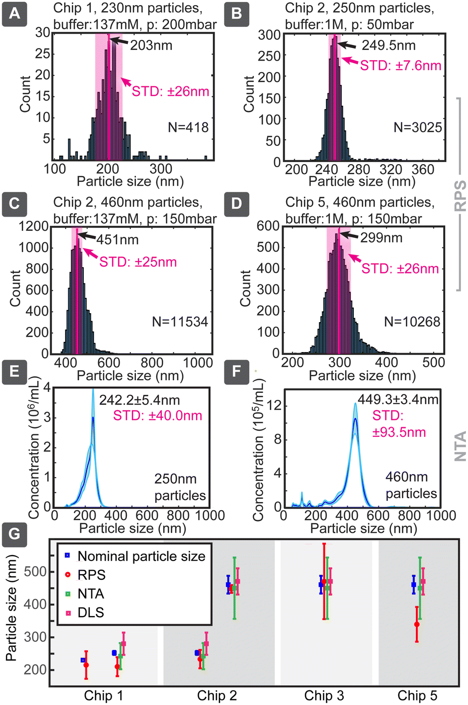 | ||
| Fig. 4 Evaluation of particle sizing capability. Particle size is calculated analytically from device geometry without calibration. (A–D) Examples of obtained distributions of particle sizes with mean value and standard deviation. (E and F) Comparison with NTA. (G) Comparison of different chips used to measure particle sizes, nominal values and measurements with commercial NTA and DLS systems (error bars indicate one standard deviation, values for RPS are based on N = 7 devices). | ||
Chip 2 could be considered the best performing, with size estimates of 233 ± 28 nm for 252 ± 6 nm and 447 ± 12 nm for 460 ± 27 nm particles, respectively. The measured and nominal reference values agreed without calibration within less than 8% difference. This good agreement can be due to the longer pore (smooth nanochannel) of chip 2, which, even though increasing the overall resistance, would make the pulses longer and would allow more accurate determination of their correct amplitude, while reducing the distribution width and errors caused by electronic noise of short spikes. For example, when chip 1 produced 0.3 ms spikes, chip 2 did 1 ms, which at 20 kHz sampling rate corresponded to 6 and 20 sampled data points, respectively. This difference in the number of sampled data points can increase the signal-to-noise ratio (SNR) by almost a factor of 2.
Concentration measurement
Another essential characteristic of a particle sample is its number concentration. Preferably concentration could be determined without individual calibration or an internal standard. From the theoretical consideration, concentration should be proportional to the spiking frequency when the driving pressure is maintained constant. We evaluated frequency dependence over 4 orders of magnitude of concentrations in the range between 2.9 × 10⁶ and 5.7 × 10¹⁰ particles per mL using different chips (Fig. 5) at pressure 100 mbar. This dynamic range is eventually limited at the lower end by the practical ability to collect enough spikes within a reasonable measurement time and at the higher end by having to avoid clogging and excessive overlaps of spikes. When fitting logarithms of concentration and frequency log(f) = log(b) + a·log(c), observed slopes a were approximately equal to 1 within the fitting uncertainty, which indicates that frequency–concentration relationship was indeed linear. The intercept B = log(b) of the fitting was found to be −8.84 ± 0.75, −7.05 ± 0.96, −7.02 ± 0.47 for chips 1, 2 and 5 respectively. When expressed linearly f = b·c = 10B·c, the value B = −7 ± 1 would mean that f(Hz) = 10−7·c (1 mL−1) or that 1 Hz frequency would correspond to 107 particles per mL, while uncertainty ±1 means that concentration/frequency can vary 10-fold. This result indicates that, without calibration, devices can tell the order of magnitude for the concentration over several orders of magnitude of concentrations, but cannot be more precise.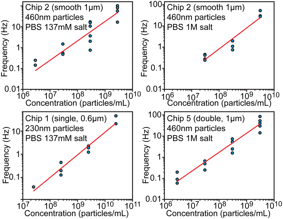 | ||
| Fig. 5 Evaluation of particle concentration. Relationship between the particle concentration and spiking frequency shown in log–log scale. | ||
The precision limitation can stem from the high sensitivity of hydrodynamic resistance, and thus of the pressure driven flow rate, on the channel geometry. Even slight obstructions or partial clogging can significantly alter the flow rate and thus the spiking frequency, while such obstructions would have only negligible effect on electrical conductivity. Therefore, calibration-free particle sizing is a lot more accurate compared to concentration measurements, but the latter could be improved with an internal standard (known concentration of added particles) as discussed in the next section. We note that inter-laboratory studies for determination of number concentration of nanoparticles have also shown large variations of about 68% in case of using particle-counting methods.24
Particle-size distribution
Combining particle sizing and concentration leads to further important capability, which is simultaneous assessment of the size distribution of various particle sizes in a mixture. It is an important capability because, on the one hand, EVs samples could be polydisperse, while, on the other hand, correct distribution ratios would also allow using an internal standard, such as spiking of a sample with a known concentration of reference particles. We assessed this capability using the chip design 2 with mixture of 252 and 460 nm particles at respective concentrations of 5.7 × 10⁹ and 2.9 × 10⁹ particles per mL (ratio: 1.97:1) (Fig. 6). The evaluation yielded clearly separated narrow populations of spikes, which without calibrations had means at 225 nm and 426 nm, being shifted 27 nm and 34 nm (or 12% and 8%) below the nominal specified values. If we use the larger population as a known reference, the corrected size of the smaller population would be 243 nm, deviating only 9 nm (3.7%) from the specified dimension. The ratio of the numbers of spikes corresponding to the small and large particles was 1.43, which is 38% lower than 1.97 expected from the nominal sample concentrations. The reason could be baseline noise, due to which some spikes corresponding to small particles were dismissed by the detection algorithm. In comparison, when we used the multimodal sample in NTA, the concentration was detected well with only <20% deviation, while size distribution suffered significant distortions for 460 nm particles (Fig. 6D), and DLS dismissed, expectedly, the smaller population (Table S7†). This finding also well agrees with previous studies,25,26 which have shown challenges of using NTA for resolving multimodal samples of polystyrene beads.
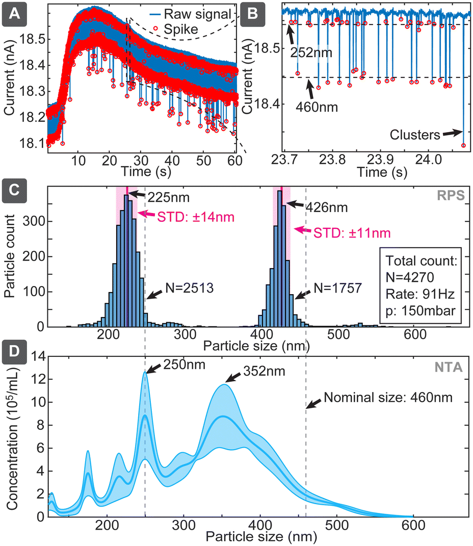 | ||
| Fig. 6 Size and concentration distribution measurement in polydisperse samples represented by mixture of 252 nm and 460 nm particles in respective concentrations of 5.7 × 10⁹ and 2.9 × 10⁹ particles per mL. (A) Raw measured signal (blue) with detected particles indicated with red. (B) Same in enlarged scale. (C) Histograms of populations of spikes corresponding to both sizes of particles, while (D) shows NTA measurement of mixture of same particles (108 particles per mL each). | ||
Measurement success rate
For practical utility of the technology, the experimental yield and robustness are equally important characteristics. Therefore, we also assessed combinations of different designs, experimental settings, and particle sizes for the ratios of successful experiments (Fig. 7) and failures, as well as to identify types of failures. The failure modes are further described in ESI† Section S5 (“Failure analysis”). After optimization of hPDMS, the fabrication yield of chips was overall high and only rarely nanochannels had cracks, which could be easily determined by observing a high, often saturated, baseline current. Other failures could be i) trapped bubbles, which when pushed through the pores would produce very high amplitude periodic pulses that are clearly distinguishable from spiking from the particles; ii) highly unstable baseline, which hinders particle detection; and iii) clogging.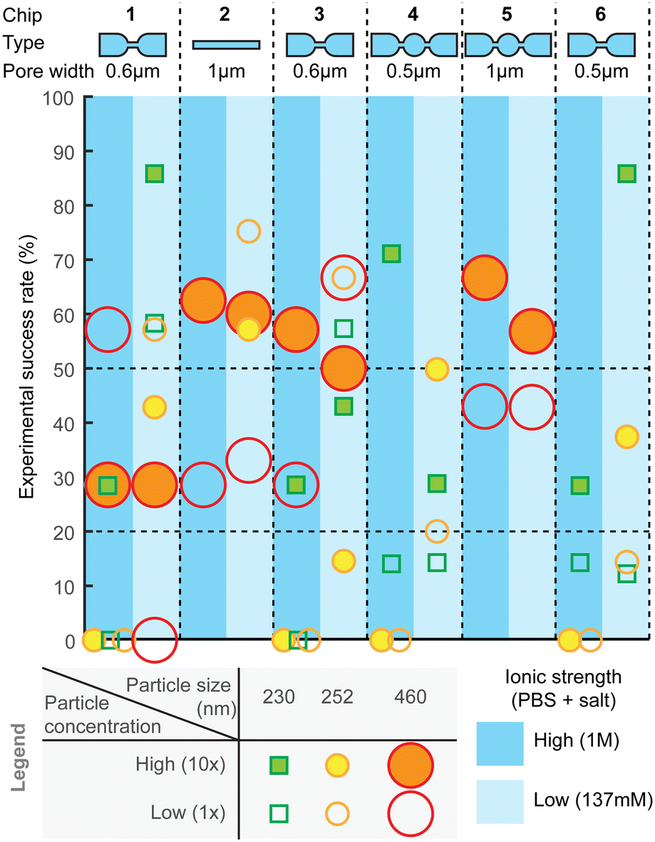 | ||
| Fig. 7 Analysis of experimental success rate. Measurements were performed with all types of nanopores using three different particle sizes at two different particle concentrations and two different PBS buffers. For the statistics each indicated measurement was performed at least N > 7 times. High particle concentration (solid marker) is 10 times higher than low concentration (empty marker), while two buffers had salt concentrations 1 M (dark blue) and 137 mM (light blue). | ||
Compared to other failure modes, clogging was the most frequent and also more difficult to detect. Small obstruction would have only a very minor effect on the baseline current and even on the spike amplitude, while they can substantially affect sample flow through the pore, because fluidic resistance depends on the channel dimensions ∝ r4, while electrical resistance only as ∝ r2. Clogging could be observed as abrupt stopping or reduction of spiking, sometimes accompanied with a small drop in the baseline current. Clogging can be partial and reversible and can happen several times during the measurement; sometimes it can be resolved by changing the pneumatic pressure.
In order to detect the clogging events, we visualized statistics of average spike width and spiking frequency in small time intervals (e.g. one or few seconds) during data processing. In normal operation both would remain constant throughout the measurement, while clogging would increase the average spike width, as well as reduce the spiking frequency as seen, for example, in Fig. S9.† Spike width can be additionally used to assess the flow velocity in the pore, as the pore length is known. Yet, partial clogging would have usually no effect on spike amplitude. Therefore, concentration measurement is more sensitive to partial clogging, while size measurement is not, in agreement with previous discussions.
Overall, across all the different chip designs, the low-ionic-strength medium (137 mM salt) produced higher success rate, compared to the higher (1 M) counterpart (Fig. 7). On average, the highest success rate was obtained with chip design 2, for which over 50% of the attempts resulted in equally successfully measuring both smaller and larger particles. Designs 1 and 3 with 600 nm pores could similarly well detect both particle sizes, while smaller constrictions, such as designs 4 and 6, could detect only smaller particles. Experimental success rate of ca. 50% per pore is a useful guideline also when designing a device with multiple parallel pores, which could then increase the likelihood of obtaining a useful result per chip. For example, with 4 pores, the success rate should be over 90%.
Biological samples
Since our target application for the sensing platform was the characterization of EVs, we evaluated devices using three biological samples: EVs purified from the media of i) human colon carcinoma cell line HCT116 (ESI† Section S8.1) by ultracentrifugation (UC) and ii) human endometrial adenocarcinoma cell line HEC-1A (ESI† Section S8.2) by combination of UC and size exclusion chromatography (SEC) and iii) untreated human serum. UC is one of the most common methods for EVs isolation, however, samples purified only by UC had significant protein content (Table S8†), which was very effectively separated by SEC, yielding high purity EV sample, though with about 10-fold lower particle concentration compared to UC sample. We evaluated samples with chip designs 1 and 2, first having higher sensitivity towards the smaller and second towards larger particles (Fig. 8).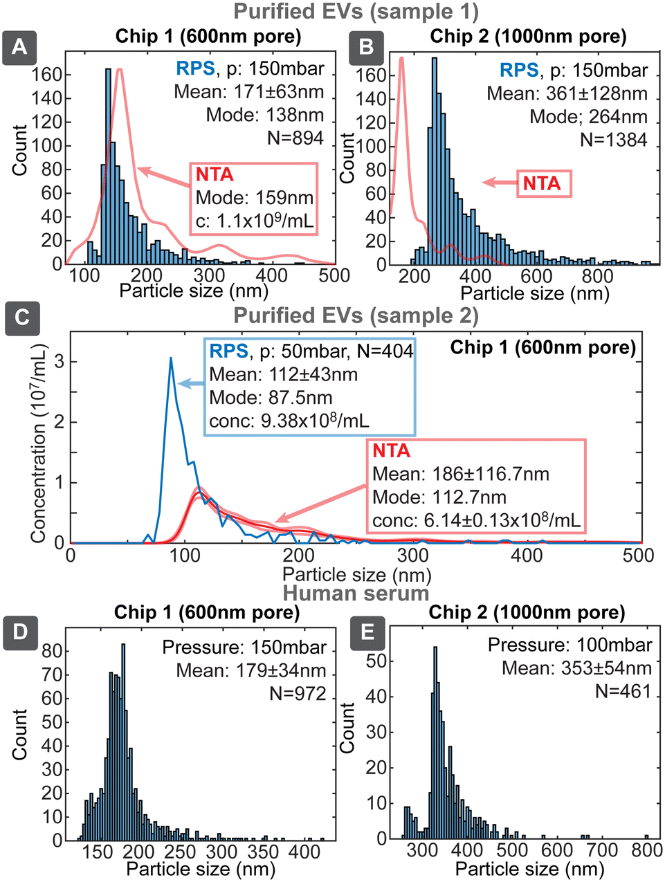 | ||
| Fig. 8 Evaluation of biological samples containing EVs. Evaluations were performed with purified EVs from two different cell culture derived preparations (A–C) and human serum (D and E), using chips 1 (A, C and D) and 2 (B and E) for respective analysis of smaller and larger populations of biological particles (EVs and proteins). NTA result on figure on A and B has arbitrary vertical scale and is intended to compare size distributions. | ||
Uncalibrated chip 1 with 600 nm pore identified the mode of distribution of the purified EVs to be 138 nm, being similar to the value of 159 nm obtained by NTA. The overall shape of the distribution was similar between our device and NTA and also resembled the previously described distributions with modes in the range 130–160 nm.27 The lower detectable size of EVs for chip 1 was about 80–100 nm. Chip 2 identified also larger particles with the mode around 264 nm, which could correspond to the 316 nm peak seen in NTA. Chip 2 had the lower size detection limit of about 200 nm, which however missed majority of the smaller EVs population. SEC purified EVs sample (2) was evaluated with chip 1 (Fig. 8C), which resulted slightly smaller mode size 87.5 nm and higher (1.5×) concentration compared to NTA 112.7 nm. This, roughly 20 nm, shift of size distribution between RPS and NTA has been also reported earlier and was explained by hydration shell of EVs.11
While unpurified serum cannot be considered EVs sample due to high concentration of other particles, such as proteins, the purpose of its use was to assess device performance in case of a complex matrix with higher viscosity. We tested serum samples both directly as well as diluted 1:1 with 137 mM PBS, where both gave similar results without clogging. The overall result resembled previous RPS measurements of blood plasma, where particle concentration decreased exponentially with increasing size in the large particle size range.28 Our devices, however, had size detection limit about 120 nm compared to about 75 nm in the previous study. This result shows that our RPS chips could be applied directly to detect EVs and other biological particles from typical EVs sources even in the presence of complex matrix.
Electronics and software
While our initial evaluation of nanopore chips was performed with a commercial patch-clamp amplifier, it requires using large and expensive equipment, i.e., does not fit our ultimate vision of a compact and affordable instrument. Therefore, we designed and produced in-house an RPS data acquisition system, described in detail in ESI† Section S6.The most critical component of the home-built system is the high-gain, high-bandwidth, and low-noise trans-impedance amplifier (TIA), able to detect small and fast current pulses, which we compared side-by-side with the commercial patch-clamp amplifier. Somewhat unexpectedly, the home-built device was able to achieve similar or even better signal-to-noise ratio (SNR) (Table S5†), which could be also due to the more effective shielding that we integrated into our system.
Considering that the pressure generator was constructed from components with cost <70 EUR, the total cost of an RPS measurement instrument could be less than 170 EUR, when also substituting a DAQ card with an ADC chip, as described and analyzed in ESI† Section S10. Finally, to obtain results in an automated manner, an RPS system also requires data processing software, which we developed in MATLAB. The algorithm is described in detail in ESI† Section S4. It allows to load data either from commercial or from the home-built system, detects and characterizes spikes, and performs statistics. Analysis process offers a check point for users to review and confirm that automated processing had correct performance, for example, by excluding some regions of the signal manually, or reviewing detected spikes in the signal. In the final step, the user can also confirm from spike duration and frequency trends, if chip clogging had occurred.
Comparison to commercially available devices
Currently two companies, Izon Science (Christchurch, New Zealand) and Spectradyne (Signal Hill, CA, USA) have commercialized RPS technologies for nanoparticle analysis used also for EVs,11,29 but with different approaches – Izon using tuneable RPS (TRPS), while Spectradyne using microfluidics (MRPS). We have compared technical specifications of these systems in ESI† Section S11. Our presented work is related to the microfluidic approach with similar characteristics, such as calibration-free operation. Spectradyne however offers selection of 5 different cartridges, which together enable particle sizing in much wider range (50 nm–10 μm) compared to our work, focused only on sizes relevant to typical EVs analysis (about 80–500 nm) with two different pores (chip 1 and 2). The components cost of our system is significantly lower compared to the sales price of commercial devices. This work provides also detailed description of fabrication, operational settings and data processing algorithms, while commercial devices have proprietary designs. Up to our knowledge open-source RPS systems have not emerged yet. Therefore, we believe that this paper provides useful guideline for those, who would like to design or RPS functionality, for example, for integration into other microfluidic systems.Conclusions
This paper describes an RPS measurement system intended for characterization of biological particles, such as EVs. This system is based on a microfluidic device, fabricated by soft-lithography, offering easy and low-cost laboratory replication. Here we have first evaluated and optimized different nanopore designs and experimental conditions for characterization of various test particles and biological samples. Particle sizes could be measured even without calibration samples; our devices can measure an order of magnitude for concentration, while being more accurate for the shape of distribution. For practical usage, we have also studied failure modes and experimental success rates using different designs and prepared home-made electronic system for low-cost and compact alternative to commercial instruments. Since the measurement is based on a microfluidic chip, this RPS functionality could be also used as a component in more integrated device together with sample preparation or other characterization techniques. Flexibility to design circuits would also allow one to combine various nanopores in the same chip, in order to ensure higher experimental success rate and accuracy as well as to increase the dynamic range of sizes. We hope that this systematic evaluation will serve as a useful design guideline for developing future integrated devices for the analysis of EVs.Data availability
Processed data supporting this article has been included in ESI.† Further raw data is available from the corresponding authors upon reasonable request.Author contributions
MC and DA: preparation of chips, measurements, data analysis; TL: preparation of EVs sample and comparison with standard techniques; CC: microfabrication process of the master, review and editing; CM: design and fabrication of home-made readout electronics, review and editing; CH: preparation of EVs sample; JP: design of home-made readout electronics; LM: conceptualization; DP: conceptualization, project administration, review and editing; LD: conceptualization, review and editing; AA: conceptualization, chip design, methodology, software development, data analysis, supervision, original draft, review and editing.Conflicts of interest
There are no conflicts to declare.Acknowledgements
We would like to thank: INL Cleanroom facility team Helder Fonseca, Tiago Oliveira, Joana Santos, Patricia Sousa, José Fernandes and George Junior for their assistance with microfabrication of the master mold; Martin Lopez and Francisca Guedes for help with nanoparticles; Patricia Monteiro and University of Minho Life and Health Sciences Research Institute (ICVS) for the access to the patch-clamp setup; We are grateful to NOVA School of Science and Technology and Prof. Hugo Aguas for educational collaboration. We are thankful for Portuguese National Innovation Agency (ANI) for financial support through project COUNTED (POCI-01-02B7-FEDER-050226). The authors acknowledge the financial support of the project Health From Portugal, with the reference no. C644937233-00000047, co-funded by Component C5 – Capitalization and Business Innovation under the Portuguese Resilience and Recovery Plan, through the NextGenerationEU Fund.Notes and references
- A. G. Yates, R. C. Pink, U. Erdbrügger, P. R. M. Siljander, E. R. Dellar, P. Pantazi, N. Akbar, W. R. Cooke, M. Vatish, E. Dias-Neto, D. C. Anthony and Y. Couch, J. Extracell. Vesicles, 2022, 11, e12151 CrossRef CAS PubMed.
- A. G. Yates, R. C. Pink, U. Erdbrügger, P. R. M. Siljander, E. R. Dellar, P. Pantazi, N. Akbar, W. R. Cooke, M. Vatish, E. Dias-Neto, D. C. Anthony and Y. Couch, J. Extracell. Vesicles, 2022, 11, e12190 CrossRef CAS PubMed.
- T. Liangsupree, E. Multia and M. L. Riekkola, J. Chromatogr. A, 2021, 1636, 461773 CrossRef CAS PubMed.
- K. W. Witwer, D. C. I. Goberdhan, L. O'Driscoll, C. Théry, J. A. Welsh, C. Blenkiron, E. I. Buzás, D. Di Vizio, U. Erdbrügger, J. M. Falcón-Pérez, Q. L. Fu, A. F. Hill, M. Lenassi, J. Lötvall, R. Nieuwland, T. Ochiya, S. Rome, S. Sahoo and L. Zheng, J. Extracell. Vesicles, 2021, 10, e12182 CrossRef CAS PubMed.
- E. Serrano-Pertierra, M. Oliveira-Rodríguez, M. Rivas, P. Oliva, J. Villafani, A. Navarro, M. C. Blanco-López and E. Cernuda-Morollón, Bioengineering, 2019, 6, 8 CrossRef CAS PubMed.
- K. Brennan, K. Martin, S. P. FitzGerald, J. O'Sullivan, Y. Wu, A. Blanco, C. Richardson and M. M. Mc Gee, Sci. Rep., 2020, 10, 1039 CrossRef CAS PubMed.
- W. H. Coulter, US Pat., 2656508, 1953 Search PubMed.
- R. W. DeBlois and C. P. Bean, Rev. Sci. Instrum., 1970, 41, 909–916 CrossRef.
- J. Clarke, H. C. Wu, L. Jayasinghe, A. Patel, S. Reid and H. Bayley, Nat. Nanotechnol., 2009, 4, 265–270 CrossRef CAS PubMed.
- Y. Song, J. Zhang and D. Li, Micromachines, 2017, 8, 204 CrossRef PubMed.
- Z. Varga, B. Fehér, D. Kitka, A. Wacha, A. Bóta, S. Berényi, V. Pipich and J. L. Fraikin, Colloids Surf., B, 2020, 192, 111053 CrossRef CAS PubMed.
- H. Cai, Y. Wang, Y. Yu, M. V. Mirkin, S. Bhakta, G. W. Bishop, A. A. Joshi and J. F. Rusling, Anal. Chem., 2015, 87, 6403–6410 CrossRef CAS PubMed.
- R. Pan, K. Hu, R. Jia, S. A. Rotenberg, D. Jiang and M. V. Mirkin, J. Am. Chem. Soc., 2020, 142, 5778–5784 CrossRef CAS PubMed.
- T. Takakura, I. Yanagi, Y. Goto, Y. Ishige and Y. Kohara, Appl. Phys. Lett., 2016, 108, 123701 CrossRef.
- Y. He, M. Tsutsui, R. H. Scheicher, F. Bai, M. Taniguchi and T. Kawai, ACS Nano, 2013, 7, 538–546 CrossRef CAS PubMed.
- Z. D. Harms, D. G. Haywood, A. R. Kneller, L. Selzer, A. Zlotnick and S. C. Jacobson, Anal. Chem., 2015, 87, 699–705 CrossRef CAS PubMed.
- A. Carbonaro and L. L. Sohn, Lab Chip, 2005, 5, 1155–1160 RSC.
- J. L. Fraikin, T. Teesalu, C. M. McKenney, E. Ruoslahti and A. N. Cleland, Nat. Nanotechnol., 2011, 6, 308–313 CrossRef CAS PubMed.
- D. C. Duffy, J. C. McDonald, O. J. A. Schueller and G. M. Whitesides, Anal. Chem., 1998, 70, 4974–4984 CrossRef CAS PubMed.
- N. Vogel, S. Utech, G. T. England, T. Shirman, K. R. Phillips, N. Koay, I. B. Burgess, M. Kolle, D. A. Weitz and J. Aizenberg, Proc. Natl. Acad. Sci. U. S. A., 2015, 112, 10845–10850 CrossRef CAS PubMed.
- J. Mariscal, P. Fernandez-Puente, V. Calamia, A. Abalo, M. Santacana, X. Matias-Guiu, R. Lopez-Lopez, A. Gil-Moreno, L. Alonso-Alconada and M. Abal, J. Proteome Res., 2019, 18, 1043–1053 CrossRef CAS PubMed.
- T. W. Odom, J. C. Love, D. B. Wolfe, K. E. Paul and G. M. Whitesides, Langmuir, 2002, 18, 5314–5320 CrossRef CAS.
- H.-L. Lin, W.-E. Fu and K. Ehara, Metrologia, 2019, 56, 04004 CrossRef.
- C. Minelli, M. Wywijas, D. Bartczak, S. Cuello-Nuñez, H. G. Infante, J. Deumer, C. Gollwitzer, M. Krumrey, K. E. Murphy, M. E. Johnson, A. R. M. Bustos, I. H. Strenge, B. Faure, P. Høghøj, V. Tong, L. Burr, K. Norling, F. Höök, M. Roesslein, J. Kocic, L. Hendriks, V. Kestens, Y. Ramaye, M. C. C. Lopez, G. Auclair, D. Mehn, D. Gilliland, A. Potthoff, K. Oelschlägel, J. Tentschert, H. Jungnickel, B. C. Krause, Y. U. Hachenberger, P. Reichardt, A. Luch, T. E. Whittaker, M. M. Stevens, S. Gupta, A. Singh, F. H. Lin, Y. H. Liu, A. L. Costa, C. Baldisserri, R. Jawad, S. E. L. Andaloussi, M. N. Holme, T. G. Lee, M. Kwak, J. Kim, J. Ziebel, C. Guignard, S. Cambier, S. Contal, A. C. Gutleb, J. Tatarkiewicz, B. J. Jankiewicz, B. Bartosewicz, X. Wu, J. A. Fagan, E. Elje, E. Rundén-Pran, M. Dusinska, I. P. Kaur, D. Price, I. Nesbitt, S. O'Reilly, R. J. B. Peters, G. Bucher, D. Coleman, A. J. Harrison, A. Ghanem, A. Gering, E. McCarron, N. Fitzgerald, G. Cornelis, J. Tuoriniemi, M. Sakai, H. Tsuchida, C. Maguire, A. Prina-Mello, A. J. Lawlor, J. Adams, C. L. Schultz, D. Constantin, N. T. K. Thanh, L. D. Tung, L. Panariello, S. Damilos, A. Gavriilidis, I. Lynch, B. Fryer, A. C. Quevedo, E. Guggenheim, S. Briffa, E. Valsami-Jones, Y. Huang, A. Keller, V. T. Kinnunen, S. Perämäki, Z. Krpetic, M. Greenwood and A. G. Shard, Nanoscale, 2022, 14, 4690–4704 RSC.
- W. Anderson, D. Kozak, V. A. Coleman, Å. K. Jämting and M. Trau, J. Colloid Interface Sci., 2013, 405, 322–330 CrossRef CAS PubMed.
- R. Vogel, J. Savage, J. Muzard, G. Della Camera, G. Vella, A. Law, M. Marchioni, D. Mehn, O. Geiss, B. Peacock, D. Aubert, L. Calzolai, F. Caputo and A. Prina-Mello, J. Extracell. Vesicles, 2021, 10, e12052 CrossRef CAS PubMed.
- Y. Ma, T. Yoshida, K. Matoba, K. Kida, R. Shintani, Y. Piao, J. Jin, T. Nishino and R. Hanayama, Sci. Rep., 2021, 11, 13471 CrossRef CAS PubMed.
- M. Cimorelli, R. Nieuwland, Z. Varga and E. van der Pol, PLoS One, 2021, 14, e0249603 CrossRef PubMed.
- J. C. Akers, V. Ramakrishnan, J. P. Nolan, E. Duggan, C. C. Fu, F. H. Hochberg, C. C. Chen and B. S. Carter, PLoS One, 2016, 11, e0149866 CrossRef PubMed.
Footnotes |
| † Electronic supplementary information (ESI) available. See DOI: https://doi.org/10.1039/d4lc00364k |
| ‡ Current address: Lund University, Lund, Sweden. |
| This journal is © The Royal Society of Chemistry 2024 |