
 Open Access Article
 This Open Access Article is licensed under a
 Creative Commons Attribution 3.0 Unported Licence
Measurement of Fe emission spectrum from 170 nm to 600 nm with a coma-free spectrometer†
Chu
Li
a,
Guo-Qiang
Xia
b,
An-Qing
Jiang
a,
Jiu-Chun
Ren
a,
Er-Tao
Hu
c,
Jian-Ke
Chen
a,
Qiao-Chu
Zhang
g,
Lei
Yu
g,
Osamu
Yoshie
d,
X.-D.
Xiang
 b,
Hai-Bin
Zhao
a,
Yu-Xiang
Zheng
a,
Song-You
Wang
a,
Yue-Mei
Yang
a,
Wei
Wei
c,
Young-Pak
Lee
e,
Junpeng
Guo
f,
Yun-Hai
Jia
g and
Liang-Yao
Chen
*a
b,
Hai-Bin
Zhao
a,
Yu-Xiang
Zheng
a,
Song-You
Wang
a,
Yue-Mei
Yang
a,
Wei
Wei
c,
Young-Pak
Lee
e,
Junpeng
Guo
f,
Yun-Hai
Jia
g and
Liang-Yao
Chen
*a
aDepartment of Optical Science and Engineering, Fudan University, Shanghai, China. E-mail: lychen@fudan.ac.cn
bDepartment of Material Science and Engineering, SUSTC, Shenzhen, China
cSchool of Optoelectronic Engineering, NUPT, Nanjing, China
dGraduate School of IPS, Waseda University, Fukuoka, Japan
eDepartment of Physics, Hanyang University, Seoul, Korea
fDepartment of Electrical and Computer Engineering, University of Alabama in Huntsville, Huntsville, AL 35899, USA
gCentral Iron & Steel Research Institute, Beijing, China
First published on 16th January 2024
Abstract
A coma-free superhigh spectral resolution optical spectrometer was successfully designed and constructed for practical application. The spectrometer consisted of 20 subgratings and a 2D BSI-CMOS array detector. The spectra were 20-fold with the physical size of the photoelectron detection along the diffraction direction and extended by a factor of 20 to achieve a spectral resolution of 0.01 nm per pixel without any moving parts. Ultrahigh dense emission lines of a hollow cathode Fe lamp were measured. Based on the data analysis and discussions, among the highly resolved spectral lines of Fe measured with an improved signal-to-noise ratio in the 170–600 nm spectral region, 2451 lines were identified in accordance with the reported ones in the literature; however, more than 1100 lines with lower intensity remained unassigned with an unknown mechanism of their origins. Our experimental data indicated the need to more fundamentally study and explore the spectral data of the Fe atoms with the potential for broad application prospects for Fe-based materials in the future.
Introduction
The mechanism of high-temperature superconductivity still requires further study in the frontier research of condensed matter physics. In 2008, Hideo Hosono et al. reported the existence of 26 K superconductivity in a fluorine-doped LaFeAsO system, which stimulated a great amount of research on Fe-based high-temperature superconductors worldwide.1 The new discovery accompanied by the research of Fe-based superconductors facilitated the understanding of the possible origin of how the electron configuration of the Fe atom plays a significant role and results in its high-temperature superconductivity in nature.2–5 Thus, investigating the electron orbital structures of the Fe atom can provide insight into the mechanism of Fe-based superconductors and other materials. The Fe atom is also one of the key and fundamental elements of Fe-based alloys widely applied in modern industry. The composition and fine atomic structures of materials can be determined by measuring and analyzing the optical spectra of reflection, transmission, absorption and so on.6–9 The atomic spectra emitted from the transition of electrons between different energy levels can also be precisely measured with high resolution characteristic of the “fingerprints” of matter.Transition metals generally show very rich atomic emission lines in the spectral region below 600 nm. For the Fe-group elements, thousands of lines are observed in the spectral region from the vacuum-ultraviolet (VUV) to the infrared due to the characteristic of the partially filled d-orbitals of the Fe group elements.10,11 Studies on Fe spectral lines are also very important to thoroughly explore the properties of the absorption spectra of many astrophysical objects, including stars and galaxies.12–14
In previous works, both grating spectrometers and Fourier transform spectrometers (FTS) were generally used to measure the atomic emission spectra of the transition metals that possess multiple spectral lines.15–18 Research has mainly focused on FTS to measure the spectral lines of transition metals in recent years due to its high resolution in the ultraviolet (UV) to infrared (IR) spectral regions.19 The resolution of the FTS is highly dependent on the precise control of the mechanically step-moving parts with software interpretation of the data in the system.19 The step-moving parts have difficulty to achieve very high-precision control in the short wavelength UV and visible regions, and thus, FTS measurements are usually carried out in large research laboratories with better experimental conditions. In addition, as shown in Fig. 1, Clear showed the spectra of a Ni hollow cathode lamp measured at the 217.45–218.15 nm spectral region using the FTS and the grating spectrometer in his Ph. D. thesis.20 Compared to FTS, the grating spectrometer had a lower resolution power with a broader full width half maximum (FWHM) of the spectral lines, resulting in spectral lines in some regions overlapping and not being fully resolved. In contrast, the FTS spectra could sharply distinguish the spectral lines due to its high resolution. However, some spectral lines observed clearly in the spectra measured by the grating spectrometer were entirely missing in the spectra of FTS.20 Hinkle et al. also noted that the measurements using the FTS could not provide a high dispersion solution, and therefore, the lines in the noise of the atlas were barely visible.21
 | ||
| Fig. 1 FTS and Grating spectra of a nickel-helium hollow cathode lamp. The inset is a partially enlarged schematic of the FTS spectrum.20 | ||
The studies of the electron orbital structures of the Fe atom will not only help to understand the mechanism of iron-based superconductors and other materials but are also very important to explore the properties of the absorption spectra of many astrophysical objects, including stars and galaxies.1–5,10–14 To date, the optical spectra with respect to the energy transitions between different electron orbits of the Fe atom have been most extensively measured and studied in broad spectral regions by using different experimental approaches.15–19 A total of approximately 37![[thin space (1/6-em)]](https://www.rsc.org/images/entities/char_2009.gif) 000 spectral lines are reported in the literature, but among them, the origins of approximately 11500 lines, equal to approximately one-third of the total lines, are still unidentified.19
000 spectral lines are reported in the literature, but among them, the origins of approximately 11500 lines, equal to approximately one-third of the total lines, are still unidentified.19
The grating spectrometer plays a significant role in acquiring rich photonic information of materials in modern science and technology, such as that in the material science, biotech and medical science fields.22–24 In the early stage of spectrometer development, mechanical control of the grating azimuthal rotation was used to change the grating diffraction angle to achieve wavelength selection with output of monochromatic light. Due to the relatively poorer long-term stability of the mechanically rotating optical elements to be operated in the broad wavelength region, it was difficult to meet the demand of high data acquisition speed in the spectral measurement. Therefore, instead of rotating planar gratings, in the development of modern optical analysis systems, integrated grating modules were used to simultaneously obtain spectral imaging consisting of multiple subwavelength regions without any mechanical moving parts in the application.25,26
These integrated modules greatly improved the measurement speed. However, as shown in Fig. 2, in typical Czerny–Turner (C–T) grating spectrometers, the off-axis optical configuration leads to image aberrations along the optical path of the system that seriously affect the imaging quality over the entire spectral range. In addition, as Gillian Nave et al. reported, to achieve high resolution in the experiment, the C–T configuration of the spectrometer required a very long focal length of 10.7 m in the system design.19 This also has led to the stagnation of research on the measurement of high-density spectral lines by grating spectrometers. To solve this problem, in this work, we designed and constructed a new type of coma-free grating spectrometer with superhigh resolution to measure the atomic emission spectra of a hollow cathode Fe lamp in the 170–600 nm spectral region.
 | ||
| Fig. 2 Schematic of the typical C–T configuration of the grating spectrometer. | ||
Principle
Coma aberration is a hard optical error issue that seriously affects the spectral resolution and sensitivity in practical applications and has not been effectively solved. With respect to Fig. 2, in the first order approximation, the equation for the coma aberration Δ is as follows:27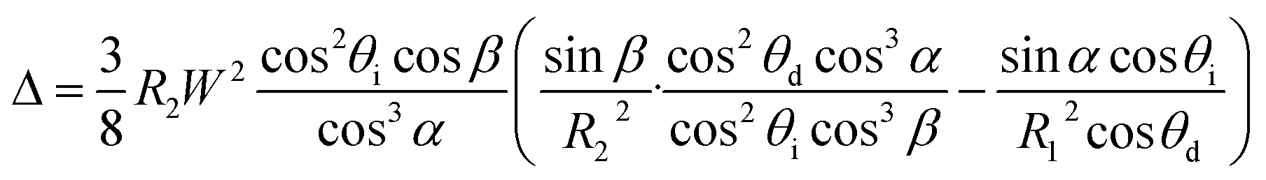 | (1) |
Different approaches have been applied to reduce coma aberrations. One approach uses a grating with a smaller size of W; however, this causes the side effect of decreasing the optical aperture, resulting in a lower number of grating lines and reducing the spectral resolution and sensitivity of the system. By analyzing eqn (1), we can use another approach that satisfies the condition in which the coma aberration Δ = 0; this results in a restricted condition as shown in eqn (2):
 | (2) |
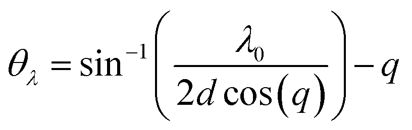
The incidence angle θi and diffraction angle θd are all correlated to be functions of wavelength λ and grating constants d, as shown by eqn (3):
 | (3) |
In previous work, in terms of using a two-dimensional (2D) back-side-illumination (BSI) CCD camera, we fulfilled the goal of designing a 44-image-folded grating spectrometer in a prototype formation consisting of three groups of gratings with groove densities of 1200 lines per mm, 1800 lines per mm, and 3600 lines per mm working in spectral regions of 600–1000 nm, 300–600 nm, and 200–300 nm, respectively.28
In this study, by taking advantage of a coma-free spectrometer with ultrahigh resolution in a broad spectral region, a new spectrometer consisting of 20 integrated gratings with grating constants g of 1800 lines per mm and a 2D BSI-CMOS array detector was designed and constructed for practical application. The CMOS detector had a pixel size of 11 × 11 μm2 and a pixel density of 2048 × 2048 with high-dynamical 16 bit-AD conversion performed in situ on the chip to achieve a high data acquisition speed of approximately 25 spectra per second. A special MgF2 transparent window was used for the CMOS array detector to be suitable to measure the data down to the wavelength of 170 nm with a peak efficiency of approximately 90% at 400 nm.
In the system design, the entire spectral region of 170–600 nm was divided into 20 subspectral regions, corresponding to 20 subgratings that were vertically distributed along the direction of the incidence slit and set at specific diffraction angles to form an integrated grating module Gx. The diffraction image of the subspectral regions could then be precisely imaged on the focal plane of the 2D BSI-CMOS detector. The size of the subgrating was 70 mm × 5.7 mm along the diffraction and slit directions, respectively, with the specific blaze wavelength λb selected and arranged in accordance with the system design to achieve the best performance of diffraction efficiency in the spectral region.
This configuration without any mechanical moving parts achieved three key functions in one spectrometer: (1) wide spectral working range, (2) high spectral resolution, and (3) high data acquisition speed.
In the test, the spectra of a dual-element Hg–Ar lamp and a hollow cathode Mn lamp were used to calibrate the spectrometer in the 170–600 nm spectral region. After, the atomic radiation from a hollow cathode Fe lamp emitting the Fe-I and F-II spectral lines was measured at room-temperature and 20 mA operation current.
Experimental configuration
A schematic diagram of the new spectrometer without coma aberration is shown in Fig. 3(a). The focal length for both spherical mirrors M1 and M2 was 500 mm. Along the diffraction and slit directions, respectively, the size of mirror M1 was 80 mm × 150 mm. To add extra flexibility in optical path alignment, 20 submirrors with the size of 120 mm × 6.5 mm for each of them were integrated to form a mirror module M2. The incident beam was collimated by mirror M1 and then entered grating module Gx under the first-order diffraction condition of m = 1. A filter set was placed between the mirror M1 and the grating module Gx and used to effectively eliminate the high-order (m ≥ 2) diffracted light corresponding to each subspectral region. The diffracted light was focused on the focal plane of the 2D BSI-CMOS array detector by mirror M2. The integrated grating module was arranged along the direction perpendicular to the incident plane, as shown in Fig. 3(b). The light was coupled into a set of optical fibres combined with an incidence slit S with a width of 10 μm and a height of approximately 0.8 mm. Because of the uneven distribution of the light intensity in the output core area of the fibre, the light intensity near the center of the beam was higher than that at the edge. Therefore, in the configuration and design of the system, the subgratings assembled in the integrated grating module Gx could be flexibly arranged. The specific arrangement is provided in Table 1. The imaging acquisition speed was greatly enhanced due to the use of the densely integrated grating module and 2D-CMOS camera. The 20 subspectral regions could then be arranged together in the calibration of the program to form a complete spectrum without any missing wavelengths or coma aberration errors. | ||
| Fig. 3 (a) Schematic of the coma-free grating spectrometer. (b) Camera with a 2D BSI-CMOS array detector placed on top of the grating module Gx with a small tilt of approximately 10° in the direction perpendicular to the diffraction plane without the coma effect. | ||
| Grating no. | Filter wavelength range (nm) | Design wavelength range (nm) | Center wavelength (nm) | Working wavelength range (nm) | Redundant wavelength range (nm) | Diffraction angle (Deg) |
|---|---|---|---|---|---|---|
| 1 | 350 | 579–600 | 589.5 | 21 | 22.81 | 22.60 |
| 2 | 350 | 558–579 | 568.5 | 21 | 23.02 | 21.30 |
| 3 | 350 | 537–558 | 547.5 | 21 | 23.21 | 20.02 |
| 4 | 350 | 516–537 | 526.5 | 21 | 23.40 | 18.76 |
| 5 | 350 | 495–516 | 505.5 | 21 | 23.56 | 17.81 |
| 6 | — | 258–280 | 269 | 22 | 24.64 | 4.23 |
| 7 | — | 236–258 | 247 | 22 | 24.67 | 3.05 |
| 8 | — | 214–236 | 225 | 22 | 24.70 | 1.87 |
| 9 | — | 192–214 | 203 | 22 | 24.71 | 0.69 |
| 10 | — | 170–192 | 181 | 22 | 24.71 | −0.48 |
| 11 | — | 280–302 | 291 | 22 | 24.60 | 5.42 |
| 12 | — | 302–324 | 313 | 22 | 24.54 | 6.62 |
| 13 | — | 324–346 | 335 | 22 | 24.48 | 7.83 |
| 14 | — | 346–368 | 357 | 22 | 24.40 | 9.04 |
| 15 | — | 368–390 | 379 | 22 | 24.31 | 10.27 |
| 16 | 350 | 390–411 | 400.5 | 21 | 24.21 | 11.47 |
| 17 | 350 | 411–432 | 421.5 | 21 | 24.11 | 12.66 |
| 18 | 350 | 432–452 | 442.5 | 21 | 23.99 | 13.85 |
| 19 | 350 | 452–474 | 463.5 | 21 | 23.86 | 15.06 |
| 20 | 350 | 474–495 | 484.5 | 21 | 23.72 | 16.28 |
Compared to the former work in designing the coma-free grating spectrometer, some improvements were made. Instead of using the CCD array detector, the 2D BSI-CMOS array detector was used to achieve high-speed data acquisition in our experiment. A set of filters was placed in front of the grating module Gx to filter the high-order (m ≥ 2) diffracted light above the wavelength of 350 nm in the 170–600 nm wavelength region. As shown in Fig. 4, one end of the lined-fiber array with the slit (10 μm) was extruded out of the small hole located at the center of the grating module Gx to avoid blocking of the light propagating along the optical path. Instead of using the toroidal mirror configuration, a new spherical mirror module M2 consisting of 20 submirrors with the same focal length of 500 mm was designed and constructed. This will keep the surface shape of mirror M2 and add extra flexibility in optical path alignment related to the grating module Gx consisting of 20 subgratings, and thus to make all 20 sub-spectra be precisely imaged on the focal plane of the 2D-CMOS array detector. In the spectral data reduction, the image Ip_background of the background noise of each pixel was measured in advance and then subtracted from the image Ip_image of the normal signal data of each pixel to obtain the real image Ir_p_image of the spectrum by suppressing the background noise more effectively in the entire spectral region according to eqn (4).
| Ir_p_image = Ip_image − Ip_background | (4) |
 | ||
| Fig. 4 Internal structure of the input light coupling through the lined fiber array in the system: (a) 3D view and (b) Front view. | ||
Therefore, without any mechanical movement parts, the new spectrometer had the advantages of compact size, good data repeatability, high reliability and long working life. It could be widely used in the fields of real-time study of spectral properties of high-performance optoelectronic materials and devices, as well as in the field of optical communication in convenience.
The 20 gratings were arranged to form a grating module. The incidence angle θλ of each grating with respect to the wavelength and system constant q (q = 10°) was fixed and determined by eqn (5) with the specific relevant parameters shown in Table 1.
 | (5) |
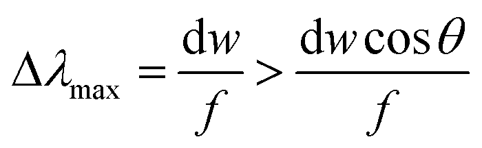
The maximum spectral resolution corresponding to the two adjacent pixels could be resolved according to eqn (6).
 | (6) |
To reduce the temperature fluctuation that will affect the resolution in the calibration and working conditions, the temperature was monitored and fixed at 24 ± 0.5 °C in the normal steel-wall-plate-sealed lab clean room condition. Thus, the reduced effect of the refractive index of air changing with temperature and humidity in the room was omitted.29
When the grating density of 1800 lines per mm was applied in the 170–600 nm wavelength region, the calculated Δλmax values were approximately equal to 0.012 nm, which was equivalent to Δλmax per pixel = 0.012 nm per pixel for the spectral resolution with respect to the theoretical prediction of the system.
Experimental results
The atomic emission spectra of the Hg–Ar, and Mn lamps were measured for system calibration according to well-known CRC data in ref. 30. From Fig. 5(a), the typical spectral lines of Hg and Ar were clearly distinguished.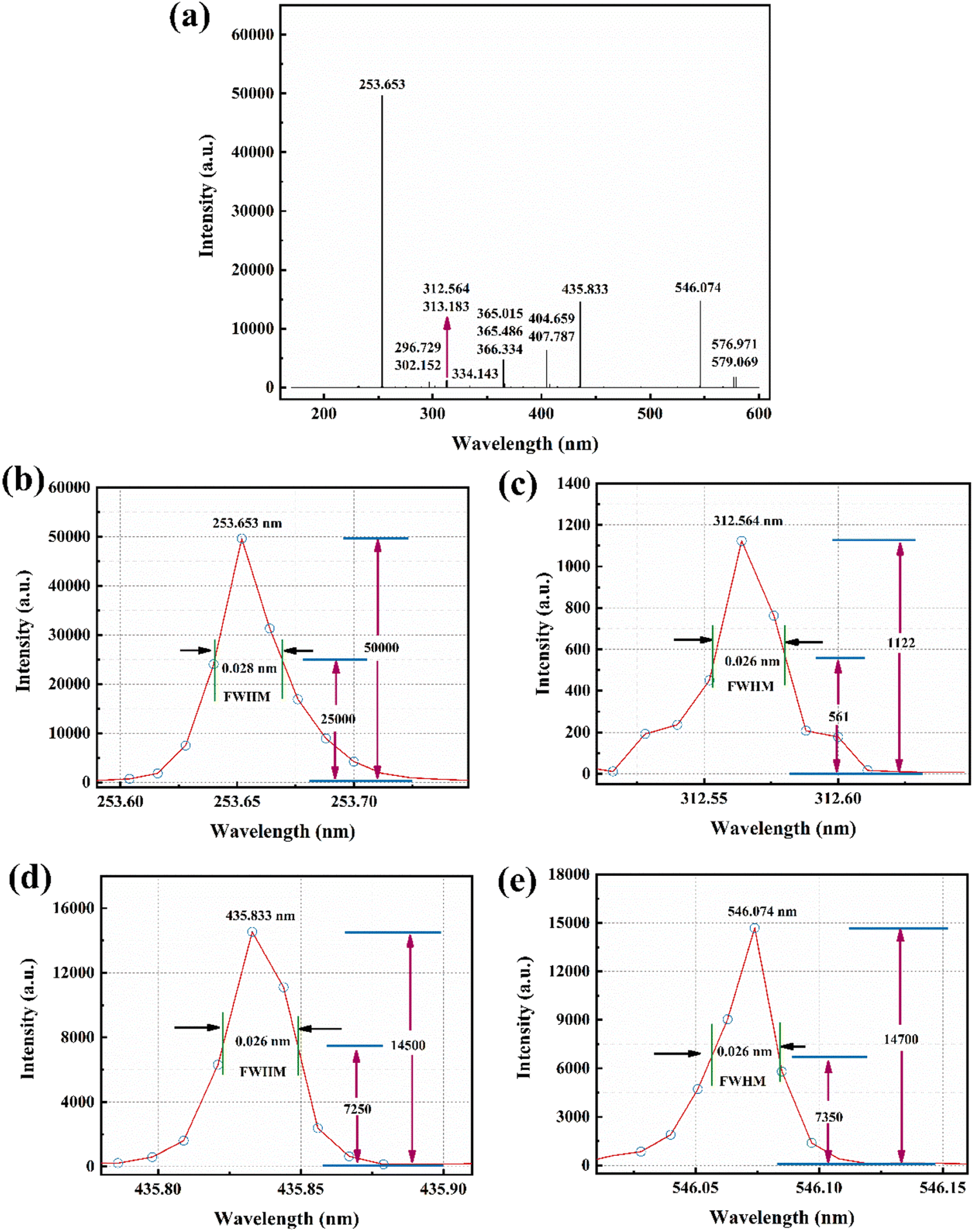 | ||
| Fig. 5 (a) Full spectra of the Hg–Ar lamp measured in the 170–600 nm spectral region. (b–e) Experimentally measured data for ΔλFWHM of approximately 0.028 nm, 0.026 nm, 0.026 nm and 0.026 nm for the lines of 253.653 nm, 312.564 nm, 435.833 nm and 546.074 nm, respectively; the pixel resolution (ΔλFWHM/3) is uniformly better than approximately 0.01 nm per pixel in the entire spectral region and is in good agreement with the design expectation. | ||
To evaluate the spectral resolution of the spectrometer, the spectral lines of the Hg–Ar lamp with relatively fine and clean characteristics at 253.653 nm, 312.564 nm, 435.833 nm and 546.074 nm are shown in Fig. 5(b–e), respectively. The full width at half maximum (FWHM) ΔλFWHM of a spectral line was measured to describe the spectral resolution. To measure the ΔλFWHM data, a spectral line generally needs to be represented by at least three pixels. The experimentally measured data of ΔλFWHM were approximately 0.028 nm, 0.026 nm, 0.026 nm and 0.026 nm for the lines of 253.658 nm, 312.564 nm, 435.833 nm and 546.074 nm, respectively; thus, the pixel resolution (ΔλFWHM/3) was uniformly better than approximately 0.01 nm per pixel in the entire spectral region and was in good agreement with the design expectation.
A spectral data density k factor can be used to characterize the high spectral performance of the spectrometer. Without any moving part, the k factor can be defined in approximation as the ratio of the full working wavelength range of the spectrometer to the total data points presented by the pixel resolution; specifically, k = (total working wavelength range Δλ)/(pixel resolution). Therefore, the k factor was approximately 4.3 × 10⁴ in the wavelength range of 170–600 nm (Δλ = 430 nm) for the spectral data measured at one time without any moving optical elements.
Measurement of the Fe spectra and discussions
There are mainly two kinds of spectral analysis methods used to measure the atomic spectral lines of the Fe atom. One is the FTS method, which is based on the principle of the Michelson interferometer to measure the change in the interference light signal with respect to the wavelength λ and stepping space x of the moving mirror in the system. After, the spectral lines can be extracted by the mathematical algorithm of Fourier transform.17 The FTS method usually has the advantage of high spectral resolution and is more often used in the infrared region. However, as shown in Fig. 1, some spectral lines are absent and the mechanism for their disappearance is unknown.20 The spectral lines also cannot be visibly observed in the noise background for the system with a lower dispersion solution.20 In another approach, a grating spectrometer that is based on the principle of the interference of light signals interacting with high-density grating lines is used. The spectral intensity and resolution depend on the optical parameters of the system, such as the focal length, grating density, and slit width. The coma effect occurring in the C-T grating spectrometer was the key issue that caused not only a reduction in the spectral intensity and resolution of the optical system but also uncertainty in some mistakenly measured spectral lines; these spectral lines were actually attributed to the residual side effect of the coma aberration for the system design even with a 10 m-long focal length to have a feature of a very small numerical aperture.19,31,32In previous studies, some of the unidentified spectral lines of the Fe atoms in the measurement were also attributed to the thermal energy transformation that occurred in the Fe hollow cathode lamp, in which some inert gas, such as Ne, was partially filled to cause possible collisions between ionized Ne and Fe atoms in a process called energy transformation:16,33–36
| Ne+ + Fe → Ne + Fe+* + ΔE | (7) |
000 cm−1 (1.24 eV) range with a maximal probability position of 0.62 eV below the excitation energy of the Ne gas.35 Thus, for the excitation line of Ne to occur at a wavelength of approximately 600 nm (approximately 2.067 eV), the line of ΔE was most likely to be observed at approximately 1.45 eV, equivalent to a wavelength of approximately 855 nm in the infrared region.
 | ||
| Fig. 6 Schematic diagram of the thermal energy transformation between ionized Ne and Fe atoms. | ||
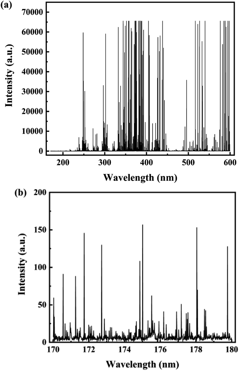 | ||
| Fig. 7 (a) Full spectra of the Fe lamp measured in the 170–600 nm spectral region with the measurement time T = 1 s. (b) Partial enlargement of the Fe spectrum shown in the 170–180 nm spectral region. | ||
In the experiment, by using a coma-free grating spectrometer with ultrahigh spectral resolution and sensitivity, we measured both the atomic spectral lines of a cathode Fe lamp partially filled by inert Ne gas and those of a pure Ne lamp in the 170–600 nm spectral range. After, the measured spectral lines of Ne as the reference were subtracted to remove the Ne spectral lines from the cathode Fe lamp from the data reduction process.
The spectral lines of the Fe atom are shown in Fig. 7(a). The Fe lamp possessed a very large number and high density of spectral lines, and a local magnification of the Fe spectrum showed that the spectrometer could clearly distinguish the multiple spectral lines in the 170–180 nm wavelength region, as seen in Fig. 7(b).
Rolf et al. reported that the final spectral data were composed of eight scans with a total scanning time of approximately one hour.37 By comparison, the entire spectral data was acquired in only 1 s with our designed coma-free grating spectrometer.
A partial enlargement of the Fe spectrum is shown in Fig. 8. The newly designed coma-free grating spectrometer greatly improved the signal-to-noise (S/N) ratio of the spectrum. All peaks with S/N ratios higher than 15 could clearly be detected by using the peak-find software.
 | ||
| Fig. 8 Weak spectral lines of the Fe atoms with S/N ratios higher than 15 and intensities over 30 clearly detected by using peak-find software. | ||
The spectra of the Fe atom measured in this study were compared with the data published in the NIST database and CRC manual with an uncertainty of less than 0.015 nm.30,38 No characteristic peaks of other impurities were found in the spectra. The specific statistics of the spectral line numbers are shown in Table 2.
| Atom species | Number of lines |
|---|---|
| Fe | 2451 |
| Ne | 279 |
| Unassigned | 1109 |
To date, there are approximately 37000 spectral lines of the Fe atom reported in the literature, but among them, the origins of approximately 11500 lines, equal to approximately one-third of the total lines, are still unidentified.19 According to the data analysis in this study, approximately 2451 spectral lines were identified in accordance with those published in the literature, while more than 1100 unassigned spectral lines were present, shown in the ESI 1–3.† For the results of unassigned lines reported in the previous studies of Fe, error sources, such as the residual coma aberration not being completely eliminated in the entire spectral region, were partly the cause for the extra weak lines observed in the experiment. The spectral resolution of the spectrometer with ultrahigh precision could still be improved to resolve those unassigned fine lines with weaker intensity that could potentially be multiply overlapped in some very narrow spectral regions.
The unassigned spectral lines all had intensities below 500 with S/N ratios higher than 15; this result indicated that more theoretical studies were needed to understand the origin of the weakly excited spectral lines of Fe atoms. The unassigned spectral lines observed with higher precision due to the elimination of coma aberrations could provide strong experimental support for further theoretical studies and explorations in the future.
Conclusion
In our study, a new zero-axis grating spectrometer without coma aberration was designed and constructed successfully. The spectrometer consisted of 20 subgratings with a 2D BSI-CMOS array detector. The spectra were 20-fold with the physical size of the photoelectron detection along the diffraction direction and extended by a factor of 20 to achieve a spectral resolution of 0.01 nm per pixel without any moving parts. Ultrahigh dense lines of a hollow cathode Fe lamp were measured. Based on the data analysis and discussions, among the highly resolved spectral lines of Fe measured with an improved signal-to-noise ratio in the 170–600 nm spectral region, 2451 lines were identified in accordance with those reported in the literature. However, more than 1100 lines with lower intensity remained unassigned with unknown mechanisms of their origins. Our experimental data indicated the need to more fundamentally study and explore the rich spectral data of Fe atoms with the potential for broad application prospects in the future.Author contributions
L. Y. C. conceived the idea for the research and supervised the project. L. Y. C., Y. X. Z., H. B. Z. and S. Y. W. designed the optical system and confirmed the parameters. C. L., G. Q. X., A. Q. J., J. K. C., X. C. Z. L. Y. E. T. H. and J. C. R. were responsible for the experiment, sample preparation, programming and data analysis. Y. M. Y. assisted in the experiment. C. L. and G. Q. X. wrote the manuscript. L. Y. C., O. Y., X. D. X., W. W., Y. P. L., H. B. Z., Y. X. Z., S. Y. W., J. P. G., and Y. H. J. discussed the results and manuscript. All authors edited and reviewed the manuscript.Conflicts of interest
There are no conflicts to declare.Acknowledgements
This work was supported by the National Natural Science Foundation of China (No. 61427815 and 62275053).References
- Y. Kamihara, T. Watanabe, M. Hirano and H. Hosono, Iron-Based Layered Superconductor La[O1−x Fx ]FeAs (x = 0.05–0.12) with Tc = 26 K, J. Am. Chem. Soc., 2008, 130, 3296–3297 CrossRef CAS PubMed
.
- H. Takahashi, K. Igawa, K. Arii, Y. Kamihara, M. Hirano and H. Hosono, Superconductivity at 43 K in an iron-based layered compound LaO1-xFxFeAs, Nature, 2008, 453, 376–378 CrossRef CAS PubMed
- K. A. Yates, L. F. Cohen, Z.-A. Ren, J. Yang, W. Lu, X.-L. Dong and Z.-X. Zhao, Point contact Andreev reflection spectroscopy of NdFeAsO0.85, Supercond. Sci. Technol., 2008, 21, 092003 CrossRef
- A. P. Drozdov, M. I. Eremets, I. A. Troyan, V. Ksenofontov and S. I. Shylin, Conventional superconductivity at 203 kelvin at high pressures in the sulfur hydride system, Nature, 2015, 525, 73–76 CrossRef CAS PubMed
- N. Hao and J. P. Hu, Topological quantum states of matter in iron-based superconductors: From concepts to material realization, Natl. Sci. Rev., 2019, 6, 213–226 CrossRef CAS PubMed
- W. Whaling, W. H. C. Anderson, M. T. Carle, J. W. Brault and H. A. Zarem, Argon ion linelist and level energies in the hollow-cathode discharge, J. Quant. Spectrosc. Radiat. Transfer, 1995, 53, 1–22 CrossRef CAS
- A. E. Kramida and G. Nave, The Ne II spectrum, Eur. Phys. J. D, 2006, 39, 331–350 CrossRef CAS
- J. F. Lei, L. B. Li, K. Du, J. Ni, S. F. Zhang and L. Z. Zhao, Thermo-catalytic decomposition of formaldehyde: a novel approach to produce mesoporous ZnO for enhanced photocatalytic activities, Nanotechnology, 2014, 25, 255701 CrossRef PubMed
- H. T. Zhang, R. He, L. Peng, Y. T. Yang, X. J. Sun, Y. S. Zhang, Y. X. Zheng, B. J. Liu, R. J. Zhang, S. Y. Wang, J. Li, Y. P. Lee and L. Y. Chen, Interpretation of Reflection and Colorimetry Characteristics of Indium-Particle Films by Means of Ellipsometric Modeling, Nanomaterials, 2023, 13, 383 CrossRef CAS PubMed
- S. Johansson, The spectrum and term system of Fe II, Phys. Scr., 1978, 18, 217–265 CrossRef CAS
- G. Nave, S. Johansson, R. C. M. Learner, A. P. Thorne and J. W. Brault, A new multiplet table for Fe I, Astrophys. J., Suppl. Ser., 1994, 94, 221 CrossRef CAS
- S. J. Adelman and D. S. Leckrone, On the need for spectroscopic data in ultraviolet stellar spectral synthesis calculations, Phys. Scr., T, 1984, 25–27 CrossRef CAS
- T. A. A. Sigut and A. K. Pradhan, Predicted Fe ii emission-line strengths from active galactic nuclei, Astrophys. J., Suppl. Ser., 2003, 145, 15–37 CrossRef CAS
- G. Nave and C. Clear, Reference wavelengths of Si II , C II , Fe I , and Ni II for quasar absorption spectroscopy, Mon. Not. R. Astron. Soc., 2021, 502, 5679–5685 CrossRef CAS PubMed
- S. Johansson and U. Litzén, Analysis of 4d-4f Transitions in Fe II, Phys. Scr., 1974, 10, 121–129 CrossRef CAS
- E. Biémont, S. Johansson and P. Palmeri, The lowest 5g-6h supermultiplet of Fe II, Phys. Scr., 1997, 55, 559–564 CrossRef
- G. Nave, S. Johansson and A. P. Thorne, Precision vacuum-ultraviolet wavelengths of Fe II measured by Fourier-transform and grating spectrometry, J. Opt. Soc. Am. B, 1997, 14, 1035 CrossRef CAS
- A. J. Ross, P. Crozet, A. G. Adam and D. W. Tokaryk, A uranium atlas, from 365 to 505 nm, J. Mol. Spectrosc., 2020, 369, 111270 CrossRef CAS
- G. Nave and S. Johansson, The Spectrum of Fe II, AJ, 2013, 204, 1 Search PubMed
-
C. P. Clear, The Spectrum and Term Analysis of Singly Ionised Nickel, 2018, pp. 1–277 Search PubMed
- K. H. Hinkle, R. R. Joyce, A. Hedden and L. Wallace, Wavelength Calibration of Near-Infrared Spectra, PASP, 2001, 113, 548 CrossRef
- R. Washington, M. Todd, N. J. Middleton and A. S. Goudie, Dust-Storm Source Areas Determined by the Total Ozone Monitoring Spectrometer and Surface Observations, Ann. Assoc. Am. Geogr., 2003, 93, 297–313 CrossRef
- A. J. R. Heck, Native mass spectrometry: a bridge between interactomics and structural biology, Nat. Methods, 2008, 5, 927–933 CrossRef CAS PubMed
- X. Zhang, Q. Li, Z. Xu and J. Dou, Mass spectrometry-based metabolomics in health and medical science: a systematic review, RSC Adv., 2020, 10, 3092–3104 RSC
- K. Y. Zang, Y. Yao, E. T. Hu, A. Q. Jiang, Y. X. Zheng, S. Y. Wang, H. B. Zhao, Y. M. Yang, O. Yoshie, Y. P. Lee, D. W. Lynch and L. Y. Chen, A High-Performance Spectrometer with Two Spectral Channels Sharing the Same BSI-CMOS Detector, Sci. Rep., 2018, 8, 12660 CrossRef PubMed
- A. Q. Jiang, K. Y. Zang, H. T. Tu, J. K. Chen, W. J. Lu, O. Yoshie, X. P. Wang, X.-D. Xiang, Y. P. Lee, B. Chen, Y. X. Zheng, S. Y. Wang, H. B. Zhao, Y. M. Yang and L. Y. Chen, Ultrahigh-resolution spectrometer based on 19 integrated gratings, Sci. Rep., 2019, 9, 10211 CrossRef PubMed
- J. Reader, Optimizing Czerny–Turner Spectrographs: A Comparison between Analytic Theory and Ray Tracing, J. Opt. Soc. Am., 1969, 59, 1189 CrossRef
- H.-T. Tu, A.-Q. Jiang, J.-K. Chen, W.-J. Lu, K.-Y. Zang, H.-Q. Tang, O. Yoshie, X.-D. Xiang, Y.-P. Lee, H.-B. Zhao, Y.-X. Zheng, S.-Y. Wang, J. Guo, R.-J. Zhang, J. Li, Y.-M. Yang, W. D. Lynch and L.-Y. Chen, A coma-free super-high resolution optical spectrometer using 44 high dispersion sub-gratings, Sci. Rep., 2021, 11, 1093 CrossRef CAS PubMed
- P. E. Ciddor, Refractive index of air: new equations for the visible and near infrared, Appl. Opt., 1996, 35, 566–1573 CrossRef PubMed
-
W. M. Haynes, Lines Spectra of the Elements, CRC Handbook of Chemistry and Physics, 2016, vol. 97th edn, pp. 10–34 Search PubMed
- J. F. Verrill and E. W. Palmer, A Coma Free Spectrometer with Interferometer Attachment for Testing Diffraction Gratings, Opt. Acta, 1981, 28, 169–175 CrossRef
- Y. Zhang, Z. Zhang, H. Yang, Y. Zhang, Z. Huang and G. Jin, Broadband aberration-corrected snapshot spectrometer with a toroidal slicer mirror, Appl. Opt., 2019, 58, 826–832 CrossRef CAS PubMed
- J. M. Green and C. E. Webb, The production of excited metal ions in thermal energy charge transfer and Penning reactions, J. Phys. B: At. Mol. Phys., 1974, 7, 1698–1711 CrossRef CAS
- S. Johansson and U. Litzen, Observations of charge-transfer reactions through enhancement of spectral lines, J. Phys. B: At. Mol. Phys., 1978, 11, L703–L706 CrossRef CAS
- S. Johansson and U. Litzen, Possibilities of obtaining laser action from singly ionised iron group elements through charge transfer in hollow cathode lasers, J. Phys. B: At. Mol. Phys., 1980, 13, L253–L256 CrossRef CAS
- S. Johansson, A Comparison Between the observed and predicted Fe II spectrum in different plasmas, Phys. Scr., T, 1984, 63–69 CrossRef CAS
- R. Engleman Jr, K. H. Hinkle and L. Wallace, The near-infrared spectrum of a Th/Ar hollow cathode lamp, J. Quant. Spectrosc. Radiat. Transfer, 2003, 78, 1–30 CrossRef
- NIST, Atomic Spectra Database Lines Form, accessed 10 July 2023, https://physics.nist.gov/PhysRefData/ASD/lines_form.html.
Footnote |
| † Electronic supplementary information (ESI) available. See DOI: https://doi.org/10.1039/d3ja00342f |
| This journal is © The Royal Society of Chemistry 2024 |