
Spatio-temporal dynamics of a microsecond pulsed Grimm-type glow discharge
Ivan B.
Krstić
 *,
Bratislav M.
Obradović
and
Milorad M.
Kuraica
*,
Bratislav M.
Obradović
and
Milorad M.
Kuraica
University of Belgrade, Faculty of Physics, Studentski trg 12, P.O. Box 44, 11000 Belgrade, Serbia. E-mail: ivan@ff.bg.ac.rs
First published on 23rd November 2023
Abstract
Spatio-temporal dynamics of a Grimm-type microsecond pulsed glow discharge (μPGD), that operates in abnormal glow regime in argon at 6 mbar, is presented. The occurrence of a high current peak during the ignition of the discharge was analyzed and the importance of taking into account the displacement current was pointed out. A development of the electron excitation temperature of argon atoms and argon ions was measured at several distances from the cathode. Spatio-temporal evolution of the intensity of selected spectral lines of atoms and ions of argon and copper were measured and analyzed during the three phases of the discharge development: pre-peak, steady-state and afterglow. The spectral line emissions have different behavior during the pre-peak and the afterglow of the discharge – the lines with low upper-level energies get the maximum intensity in the pre-peak period, while the lines with high upper-level energies get the maximal intensity in the afterglow period. The time of the appearance of the afterpeak maxima and the afterpeak decay time are shorter for the ions than for the atoms. The results are explained primarily in terms of three-body recombination processes and ion mobilities. Carefully arranged and conducted experiment with a large amount of experimental data, together with analysis of excitation and deexcitation processes, could be useful for more precise modeling of μPGD, as well as a note for selection of adequate spectral lines and discharge conditions for more accurate analytical measurements.
1 Introduction
Pulsing discharges offer a number of advantages in comparison with related continuous discharges. One is to provide an additional way of controlling the discharge plasma by choosing the pulse parameters, such as pulse length and frequency, in order to select optimal discharge conditions. Several parameters can be significantly changed compared to the non-pulsed operation. For example, the amplitude of current can be orders of magnitude higher, leading to higher particle energies and higher degree of ionization of the plasma.1,2 An interesting property of the pulse discharge is that the instantaneous power, responsible for the sputtering, excitation and ionization yields can be chosen nearly independent from the average power by varying the duty cycle of the applied pulses, and pulsed discharges can use much higher power during each pulse compared to continuously operated discharges.3 In this manner, a low power source is converted into a high-power source on a short time scale. In addition, by means of pulsing, one can modulate electron and ion energy distribution functions to produce shapes that are not otherwise attainable using continuous excitation. This is possible because in a continuous mode sources and losses of all species must be in instantaneous balance while in a pulsed system, these quantities need to be balanced only in average, over the pulse period.4 All the mentioned permits pulsed discharges to act differently from continuous discharges in a number of ways allowing wide range of application. For example, it is found that the ratios of chemical species in the glow can be accurately controlled using time-modulated discharge5 and this can in turn brought an improvement of the deposition rate.6As a type of pulsed discharge, pulsed glow discharges (PGD) brought an improvement of the analytical characteristics of the GD sources for several optical and mass spectrometric methods. Advantages of PGD are increasing signal outputs and the temporal resolution of analytical species from concomitant species in the discharge plasma. Although this is obtained with a millisecond PGD, coupling the PGD with a time-of-flight (TOF) mass spectrometer and reducing the discharge to the microsecond range created additional temporal separation opportunities.7 Another benefit of the microsecond PGD (μs-PGD) is that even though instantaneous power is higher, the average power can be significantly lower than in millisecond mode, resulting in reduced thermal stress of the analyzing sample. The higher instantaneous power of the μs-PGD is closely related to the so-called electrical “pre-peak”, which is a spike in the electrical current at the leading edge of the discharge pulse.8 The electrical pre-peak can be explained by gas heating followed by gas expansion.9 The current pre-peak causes a radiation pre-peak, which is a spike of plasma radiation at the leading edge of the discharge pulse. The radiation pre-peak, together with an increased radiation in the afterglow for some spectral lines (after-peak) are responsible for the improvement of the analytical characteristics of the PGD in the optical emission spectrometry.
In this paper we present the results of the measurements of the spatio-temporal distributions of many atomic and ionic emission spectral lines of argon and copper in the Grimm-type μs-PGD.
2 Experiment
There are many different types of Grimm plasma sources10 in use today. The one used in this experiment is a modified Grimm plasma source and has already been described in details elsewhere.11,12 For the sake of completeness only some details will be given here. The 50 mm long hollow anode with inner diameter of 8.00 mm has a longitudinal slot (10 mm long and 1.5 mm wide) for plasma observation and side-on recording along the discharge axes, from the cathode up to 10 mm away from its surface. The water-cooled cathode holder has exchangeable copper electrode, 5.00 mm long and 7.60 mm in diameter, which screws into the holder to provide good electrical and thermal contact.All measurements obtained here are recorded using argon (Messer, 99.999% purity) as a working gas, at constant gas flow of 80 ml min−1 and at the gas pressure of 6 mbar, conditions that is typical for optical-emission spectrometry analysis with the Grimm-type GD source.13 To run the discharge, a laboratory made pulsed voltage power supply with capability to ensure up to 300 W per pulse was used (Fig. 1). Two negative–positive–negative (NPN) insulated gate bipolar transistors (IGBT) allowed complete insolation of the anode from a high voltage (HV) and ground. The used configuration of two IGBT enabled achievement of very fast rising and falling edges of the pulse. That enables complete separation of the power source from the discharge plasma, without discharging of the capacitors through the plasma during the afterglow phase and without parasitic capacitance, which is not taken into account by most of the studies, see e.g.13,14 Pulse frequency, pulse width and the off-time were controlled separately by programable signal generator Tektronix MDO 3032.
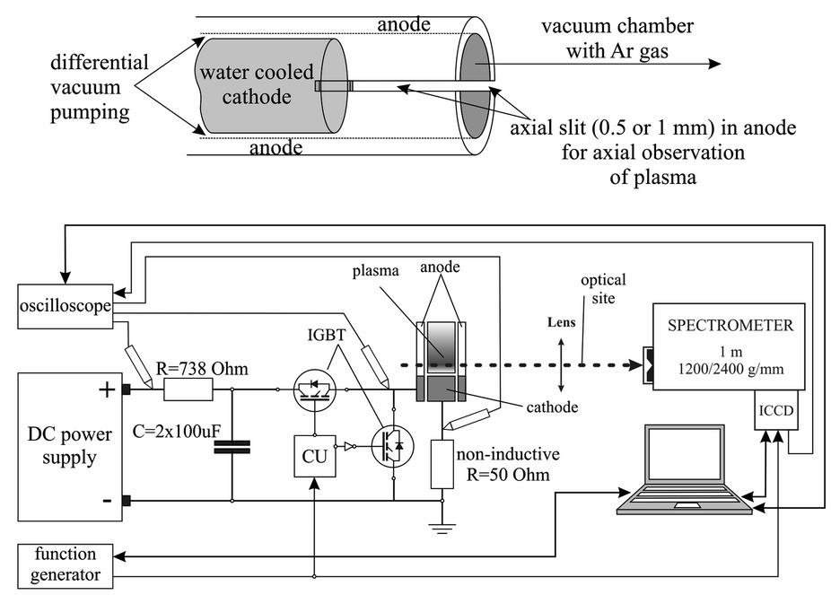 | ||
| Fig. 1 Schematic diagram of the experimental setup. | ||
For a space resolved emission measurements we used optical system contained of quartz lens (f = 150 mm) and an imaging spectrometer. 1m-Spectrometer used in the experiment is Solar MSDD 1000 with the two interchangeable gratings of 1200/2400 grooves/mm equipped with an ICCD camera (PI-MAX2, Princeton Instruments) with 1024 × 1024 pixels. The spectrometer slit width was set to 50 μm due to the low intensity of the observed light. The ICCD was triggered from the same line as control unit (CU) of the pulse power supply and build in automatic delay function.
For the monitoring and recording of the current and voltage signals, Tektronix TDS 2024B digital storage oscilloscope (200 MHz, 2 GS s−1) was employed. Current was determined as a voltage drop over 50 ohm non-inductive resistor.
This experimental setup enabled stable applied voltage pulses with a very small jitter of around 20 ns. Although the small jitter allows spectra recording using a smaller time step, very low intensity of some lines forced us to use an optimal gate width of 1 μs. The entire voltage pulse is scanned controlling the gate delay with the mentioned gate width; thus, the observed spectral intervals are recorded with 1 μs temporal resolution. On this way the recorded spectra were spatially and temporally resolved. The intensities of the spectral lines are obtained integrating specific spectral line over the wavelength which enabled presentation of the spatio-temporal distribution of the spectral line intensities, see Fig. 7–9, 12–14 and 16. Following the suggestion in,15 all measurement have done by using the frequency of 5 kHz and the pulse width of 30 μs. 170 μs off-time allowed us investigation of the near-afterglow of the discharge.
3 Results and discussions
3.1 Electrical characteristics
Grimm-type glow discharge is usually used as a source for analytical applications. For these purposes it is necessary for the discharge to operate in a mode with a homogeneous current flow through the cathode surface obtaining uniform sputtering of the cathode material. When the discharge completely covers the cathode, the increase of the voltage causes linear increase of the discharge current. Then, the discharge operates in an abnormal glow mode. In the case of pulsed Grimm-type dc discharge, voltage–current characteristics are obtained for the three values of the final pulse currents: 20 mA, 40 mA and 60 mA.Graph presented in Fig. 2 shows that the used μs-PGD operates in the abnormal mode. For a further study of the μs-PGD behavior it is important to look at the current and voltage signal shapes during the pulse. The dc pulse power supply used in this work produces an almost rectangular voltage signal with a small overshoot at the beginning of the pulse, see Fig. 3a. The power switch-on rise time measured on a noninductive resistor is about 100 ns while the rise time of the μs-PGD is 1 μs (from 5% to 95% of voltage value). The current pulse shapes for three different voltages, 30 μs pulse width, 5 kHz frequency and 6 mbar pressure, are presented at Fig. 3b. Analyzing the current pulse shapes, two effects could be noticed: the current peaks at the beginning and at the end of the pulse are immersed in several megahertz ringing and the current slowly changes between the two mentioned peaks. The high current peak at the beginning of the pulse has already been observed by other researches.16–18 Although the origin of the high current peak after the plasma ignition is still not clear,1,19 it seems that the largest part of it is due to the capacitive displacement current, caused by the rapid increase of the applied voltage. In our case dV dt−1 is about 900 V μs−1, capacitance of the Grimm discharge with cables is about 200 pF and inductance about 0.5 mH. All the mention data give the displacement current about 180 mA and estimated ringing frequency of 3 MHz, both in agreement with the measurements.
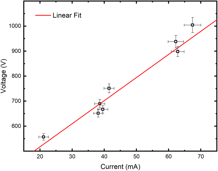 | ||
| Fig. 2 Voltage–current dependency for our configuration of μs-PGD. | ||
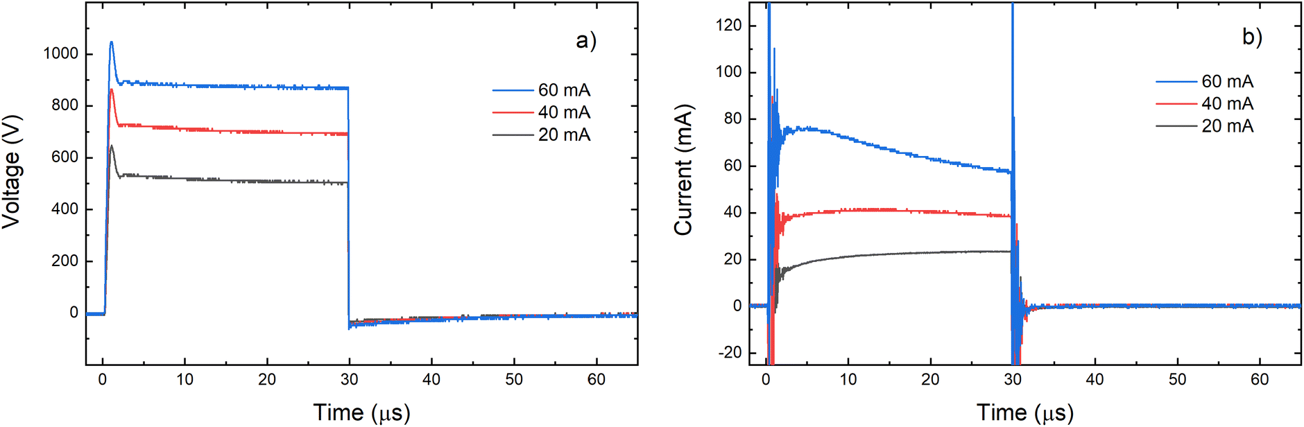 | ||
| Fig. 3 Voltage (a) and current (b) pulse profile for different voltages applied on the discharge (P = 6 mbar, f = 5 kHz, pulse width = 30 μs). | ||
3.2 Electric field distribution
The cathode region of a glow discharge includes the cathode fall (CF) and the negative glow (NG) regions. The main characteristic of the CF region is high value of E/N (electric field divided by ground state atom density) that decreases intensely along the discharge axes from the cathode. In the NG region the electric field strength is very low, close to zero. It has a high density of low-energy electrons and a low density of high-energy electrons that are injected from the CF region. The knowledge of the electric field in the CF region, where sputtered atoms are formed and excited, is necessary for the understanding of the processes that influence the spectral lines emission distributions. The measurement of the electric field is also important for the detection of the moment when the high electric field strength extinguish with respect to the power supply switch-off and the identification of the discharge transition into the afterglow regime. The electric field in the discharge can be measured using Stark splitting and shifting of hydrogen Balmer line Hβ. Hydrogen is present in the argon as an impurity, and its concentration is usually high enough to perform reliable electric field measurements during the discharge operating in the continuous regime. Unfortunately, in the used pulsed discharge, due to low intensity of Hβ line, it was not possible to measure the electric field during the discharge development without an addition of hydrogen. On the other side, addition of even small amount of hydrogen can affected the argon discharge, changing its characteristics (see (ref. 20) and the references therein). Taking this in mind, the smallest addition of 0.6% of hydrogen, that enables electric field strength measurements, is used.Fig. 4 presents two recordings of π polarized component of Hβ line (Hβ(π)) in the moments when the discharge is on (30 μs) and the first next moment when the discharge is off (31 μs). The selected profiles of Hβ(π) lines recorded very close to the cathode surface clearly show that when the discharge is on, the Hβ(π) line is split, while when the discharge is off, no splitting is observed. It means that, according to the accuracy of the method, the electric field in the afterglow regime is lower than 1 kV cm−1 (i.e. unmeasurable). In this paper we will focus on the analysis of the line intensity in the CF and the NG regions, and the best way for the estimation the border between them is the knowledge of the length of the CF. The length of the CF can be estimated using an extrapolation of the electric field distribution in the CF region. For the electric field measurement the Stark polarization spectroscopy technique is applied to Hβ(π) line (for experimental procedure of the electric field measurement see ref. 21 and eqn (14) therein). Typical profiles of Stark split Hβ(π) line recorded in CF is shown in Fig. 4c with the appropriate fit. Using the method for the determination of the electric field distribution in the CF region proposed by Wronski22,23 and within the experimental uncertainty, the end of the CF region is estimated at the distance (0.8 ± 0.1) mm, see Fig. 4c. Coupling between the CF and the NG regions is affected by the fluxes of charged particles and photons across the diffuse boundary between them through which ion motion changes from being fairly random (NG) to being substantially directed (CF).
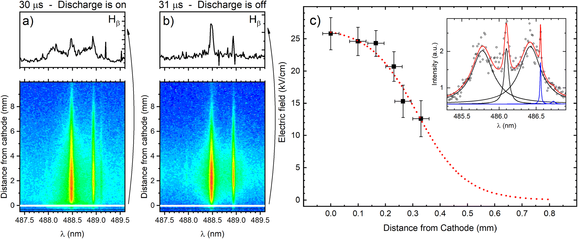 | ||
| Fig. 4 Axial profile of π component of Hβ line in two different time moment: (a) at the end of discharge pulse and (b) right after the pulse has ended. (c) Axial electric field distribution for Hβ line on time position 24 μs with the example of the fit in the inset (working gas Ar + 0.6% H2, U = 1100 V, I = 60 mA, P = 6 mbar, f = 5 kHz, pulse width = 30 μs). | ||
For the further analysis one should have in mind the discharge space is roughly divided into the two regions: the CF, which prolongs from the cathode to the distance of 0.8 mm, and the NG, from the end of the CF to the end of rest of the discharge. Unfortunately, low intensity of Hβ line did not allow us to measure the length of the CF regions for the discharges at 20 and 40 mA. According to results of the mathematical simulation of Grimm-type glow discharge, the length of CF practically does not change at the pressure of 6 mbar and for the applied voltage between 500 and 900 V,24 so we could conclude, with a fair reliability, that the CF length is the same for all the used discharge conditions.
3.3 Electron excitation temperature
The electron excitation temperatures in the argon discharge are determined from the Boltzmann plot of the 8 Ar I lines (516.23, 518.77, 573.95, 580.21, 750.39, 751.47, 810.37 and 811.53 nm) and from the relative intensities of 16 Ar II lines (362.21, 366.04, 366.96, 367.10, 368.01, 371.82, 372.04, 372.45, 372.93, 396.84, 397.94, 399.48, 403.38, 407.66, 407.96 and 408.24 nm) with transition probabilities taken from (ref. 25). Grotrian diagram of argon atom and ion lines analyzed in this work is presented in Fig. 5.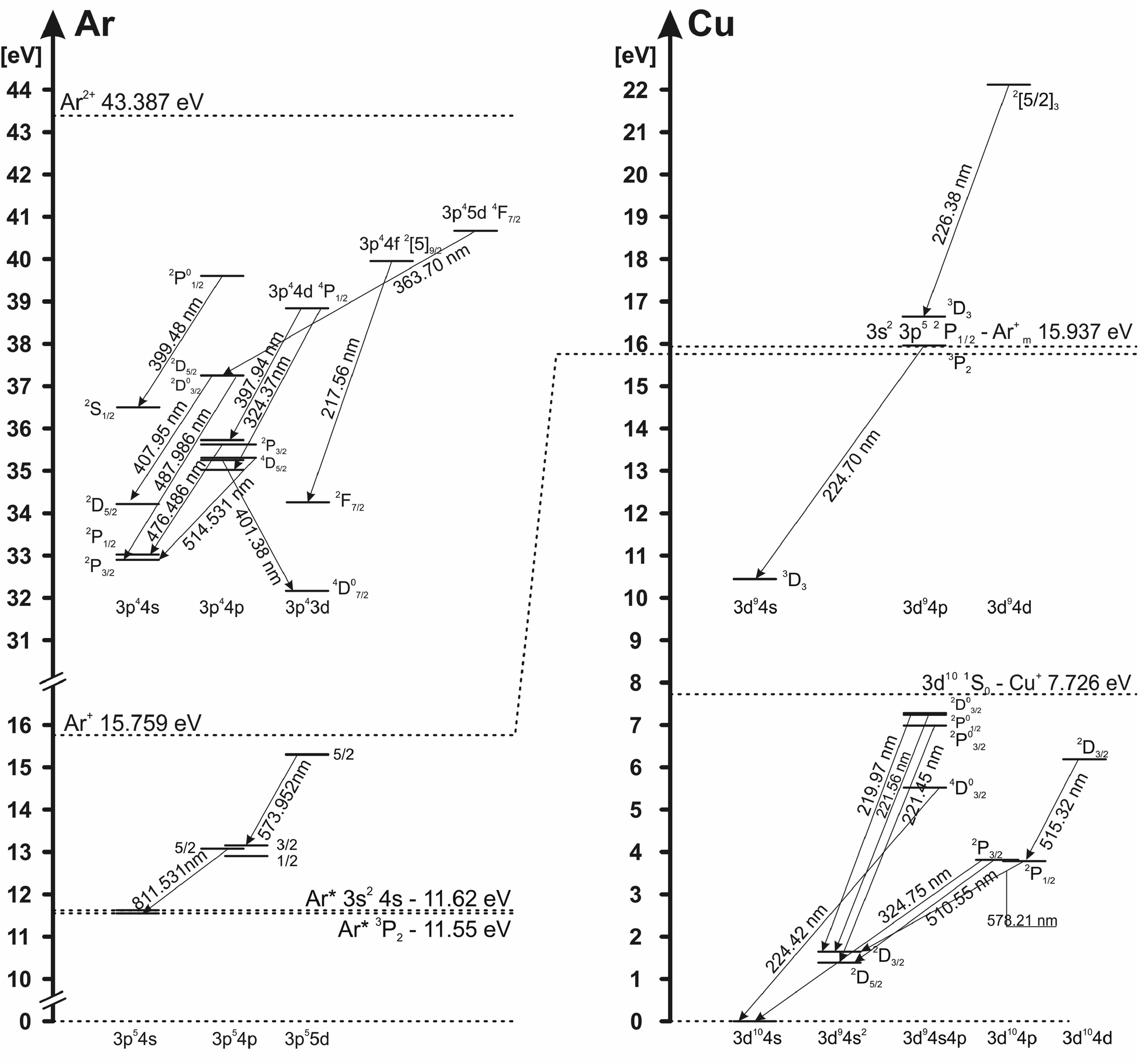 | ||
| Fig. 5 Grotrian diagram of Ar atom, Ar ion, Cu atom and Cu ion lines transaction. | ||
To determine the electron excitation temperature, the local thermal equilibrium (LTE) is assumed in the NG region. In the CF region, where charged particles accelerate and EEDF is not Maxwellian, conditions for LTE are not fulfilled, so the excitation temperature cannot be obtained by using the Boltzmann plot method. In the Boltzmann plots several spectral lines are excluded; lines that have very high intensity, because of their possible self-absorption, and Ar II laser lines (Ar II 476.49 nm, Ar II 479.99 nm and Ar II 514.53 nm) because of their ability to create population inversion. The excitation temperatures can be measured only during the active phase of the discharge (voltage-on). In the afterglow phase (voltage-off), the energy levels of atoms and ions, during the recombination, are populated from the above, causing a deviation from the Boltzmann balance giving the evidence that, for the afterglow plasma, approximation of local thermodynamic equilibrium (LTE) cannot be used. Using a relaxation method for the determining the state of equilibrium proposed by Bydder and Miller,26 Jackson and King have found that the discharge plasmas deviate significantly from LTE conditions in the afterglow phase.27 Using the same method for Ar I and Ar II lines, we have proven that in our μs-PGD, the afterglow plasma deviate from LTE, and the Boltzmann plot cannot be used for the measurement in the discharge plasma layers of the excitation temperature.
The temperature is measured parallel to the cathode surface (side-on) at the distances 1.0 mm, 2.0 mm, 3.0 mm and 5.0 mm from the cathode surface.
Fig. 6 presents the electronic excitation temperatures of argon atoms (Te of Ar I) for the different operational conditions. It shows an abruptly initial growth of Te in the early ignition phase of the discharge when the electric field is mostly determined by the geometric configuration of the electrodes and the space charge is starting to buildup. During that time the electrons obtain the highest energy and the initial jump of the electron temperature is expected (and consequently the excitation temperature) while the electron density rapidly rises by electron impact ionization of argon atoms.28 This is especially expected when the rise time of the applied power is short,29 like in our case where it is less than 1 μs, see Fig. 6a. It seems, according to large error of the Te, that the during the discharge development in the first two microsecond, the Boltzmann balance of the atomic energy levels is perturbed. This can be explained by deviation from LTE during the Ar+ ion space charge buildup and forming of NG, region where existence of LTE is expected. After the first couple of microseconds, Te of Ar I continually increases until the end of the discharge pulse (voltage of 710 V), reaching 1.1 eV at 1.0 mm distance from the cathode, see Fig. 6a. At farther distances of 2.0, 3.0 and 5.0 mm, the Te of Ar I also continually increases with time and reaches lower values of 0.8, 0.7 and 0.4 eV, respectively. The increasing of the temperature during the discharge pulse is a consequence of continuous heating up of the discharge plasma by the power supply, while decreasing the temperature along the discharge axis is caused by electron energy losing in the interactions along the NG region. At the higher voltage (880 V), Te of Ar I also continually increases during the discharge pulse, reaching a saturation value after the 15–20 μs, see Fig. 6a. Maximal temperature at 1.0 mm distance is the similar as for the lower voltage; at the farther distances the temperature decreases, see Fig. 6b, although the decrease is not so systematically evident as for the lower voltage. Comparing the temperatures, one can conclude that the increase of the input electrical power causes increasing of Te of Ar I along the discharge. Analyzing the Fig. 6c one can see that an evolution of the excitation temperature of argon ions (Te of Ar II) has a similar trend as for Te of Ar I: continuous slow increase that is noticeable faster at the beginning of the discharge, and the higher temperature for the higher voltage (input power). In the range of the experimental errors (∼20%) there are no differences between the temperatures obtained at different distances. At 710 V and 880 V the temperatures are 1.4–1.5 eV and 1.4–1.7 eV, respectively.
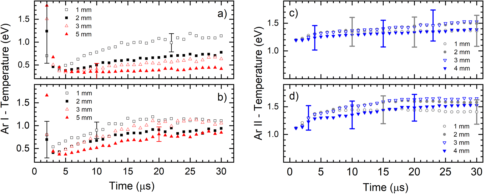 | ||
| Fig. 6 Electronic excitation temperature of Ar atoms (a and b) and Ar ion (c and d) for different axial position from cathode for two conditions (a) and (c) U = 710 V, I = 40 mA (b) and (d) U = 880 V, I = 60 mA (working gas Ar6.0, P = 6 mbar, f = 5 kHz, pulse width = 30 μs). | ||
3.4 Electron excitation temperature
The emission characteristics of the muPGD are studied to obtain insight into the excitation and recombination processes of argon, as the working gas, and copper, as the sputtered material. The shape of the spatio-temporal distributions of a spectral line intensities are consequence of the discharge development. Three characteristic phases (or muPGD regimes) can be resolved based on the line intensity distributions: the pre-peak (0–5 mu s) – the discharge breakdown followed by high current peak caused by fast increase of the applied voltage; steady-state (5–30 mu s) with the slowly changing current and the constant voltage, and the afterglow when the voltage is switched off and the current is zero. Which of the three phases will be the most prominent in the line intensity distribution depends on the particular spectral line: its energy levels and excitation processes. It has been generally observed that in the pre-peak phase the lines with upper levels of relatively low energy have higher intensities,13 while in the afterglow phase the higher intensities belongs to upper levels with higher energy.30,31 In this section we present the spatio-temporal distributions of the spectral lines that, following the mentioned general rule, are selected in a such way that first line has low energy upper level and the second line has lower energy level identical or close to upper energy level of the first line. The pair of lines are selected for argon atom and argon ion, and copper atom and copper ion. Additionally, laser lines of argon ion and a resonant line of copper atom atoms are presented. There are the two main space regions characteristic for the discharge: the CF whose border is marked as L in the following figures and the NG beyond the CF. CC is mark for close to the cathode region.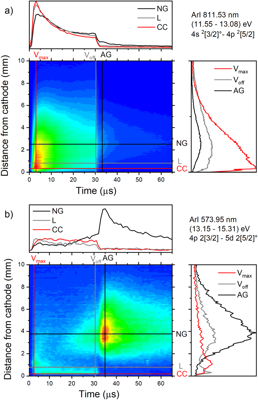 | ||
| Fig. 7 Spatio-temporal distribution of ArI (a) 811.53 nm and (b) ArI 573.92 nm spectral line (U = 880 V, I = 60 mA, P = 6 mbar, f = 5 kHz, pulse width = 30 μs). | ||
The pair of lines whose intensity distributions represent general behavior of Ar I spectral lines are Ar I 811.53 nm (4s–4p, 11.55–13.08 eV) and Ar I 217.56 nm (4p–4d, 13.15–15.31 eV). Under the operating conditions of the discharge, approximately 50% of the metastable argon atoms are thought to form via radiative decay from the 4p level.32 A lower level of Ar I 811.53 nm line is a metastable level 3s23p5(2P3/20)4s which is populated mostly by radiative decay from 4p level. The emission from a transitions that are populating the metastable level gives a good indication of the spatio-temporal distribution of the metastable argon atoms in the discharge.32 Continual decreasing of the line intensity during the discharge pulse follows the decreasing of the current, see Fig. 7a.
Analyzing the distributions of Ar I 811.53 nm line one can see that the maximum emission intensity over the entire pulse cycle comes from a positions located in the middle of the CF region, at the moment of the maximal applied voltage (marked as Vmax). The spatial distribution for the 811.53 nm line at the moment of Vmax is characterized by a dominant maximum in the CF region attributed to electron impact excitation and the lower peak, closer to the cathode, attributed to fast atom/ion impact excitation,33 see right graph in Fig. 7a. During the voltage pulse, the intensity of the first, lower peak, doesn't change its position while the second, higher peak is broadening and moving further away along the NG region, see Fig. 7a. It has been shown that in a dc discharge at the pressures up to 1 mbar first peak is always higher than the second peak33 while at 6.6 mbar first peak is lower than the second one34 which is in a qualitative agreement with our observation. In the afterglow time, the position of the maximal intensity is in the NG region and it remains unchanged during that time. The line intensity evolution profile has a maximum at the moment when the applied voltage has a peak value Vmax and continuously decreases till the end of the pulse. After the discharge switch-off, a small maximum appears in the afterglow, located in the NG region, 1.5 mm away from the end of the CF region marked as L, see Fig. 7a. This, so called after-peak, arises as a consequence of the three-body recombination processes, after the time required for the fast electrons to thermalize via collisions,27 which is in our case in order of microseconds. It is experimentally observed30,31 and predicted by the numerical model35 that the after-peak intensity is higher for the lines whose upper levels energies are higher. One more confirmation for the mentioned statement is presented by the spatio-temporal distribution of the Ar I 573.92 nm line, which upper level is 5d at 15.31 eV, more than 2 eV higher than 4p level. The notable difference in the steady state and after-peak emission intensities for this line, as compared to the previous one, illustrates the dramatic differences that the emission profiles can experience depending on the upper electronic energy level of the emitting atoms. The Fig. 7b shows that the maximal intensity during the pulse cycle (discharge and afterglow) is obtained in after-peak, at about 4 μs after the discharge is switched off. Position of the after-peak is about 4 mm away from the cathode, farther than Ar I 811.5 nm line after-peak. Position of the after-peak depends on applied voltage (current) and the after-peak distance from the cathode increases with the voltage (current) increase what can be clearly seen at Fig. 8a–c where the locations of the maxima of the after-peaks are at 2.6, 3.8 and 5.2 mm from the cathode for the applied voltages of 510, 710 and 880 V, and currents of 20, 40, and 60 mA, respectively. A reason for such distributions can be explained as follows. After the switching off the applied voltage, electrons are going to thermalize and then to recombine with argon ions through the three-body recombination process, the most responsible process for after-peak formation in μs-PGD.31 Spatio-temporal distribution of the after-peak, as a product of the three-body recombination, depends on electron density distribution, electron energy and Ar+ density distribution. Increasing voltage and current in an argon abnormal glow discharge causes increasing of Ar+ density and electron density. Increasing voltage also causes spreading electron density distribution deeper in the NG region;36 specifically the highest electron density with the widest distribution, located the deepest the NG, is expected for the highest applied voltage of 880 V. Increasing of Ar+ and electron densities increase frequency of ion-electron collisions (crucial for the recombination processes) and electron–electron collision (crucial for the electron thermalization in the afterglow24), making the electron energy thermalization the fastest for the highest current. Taking all the mentioned into account, one can conclude that for the lowest voltage of 510 V, Ar+ and the electron densities are the smallest which determines the longest recombination time. In that case, the after-peak appears 7 μs after the switching off the discharge, while with increasing the electron density, it appears earlier, 4 μs and 3 μs after switching off the discharge for 710 and 880 V, respectively, see Fig. 8a–c.
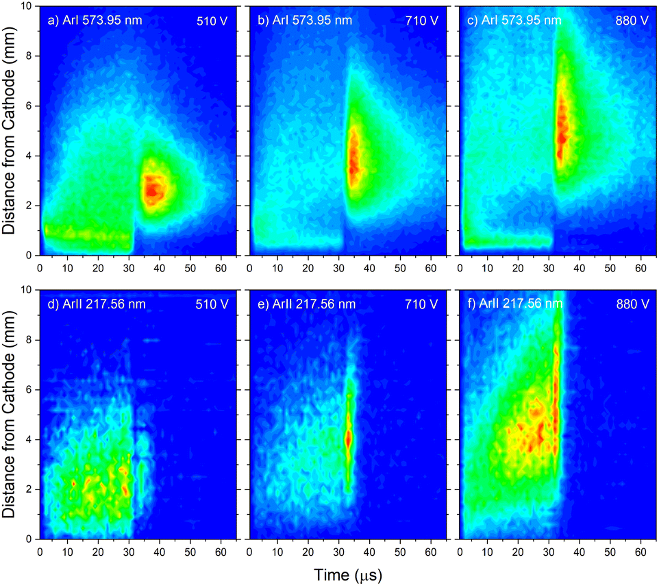 | ||
| Fig. 8 Spatio-temporal distribution of Ar I 573.92 nm (a–c) and Ar II 217.56 nm (d–f) spectral line for different voltages U = 510 V and I = 20 mA, U = 710 V and I = 40 mA, U = 880 V and I = 60 mA (P = 6 mbar, f = 5 kHz, pulse width = 30 μs). | ||
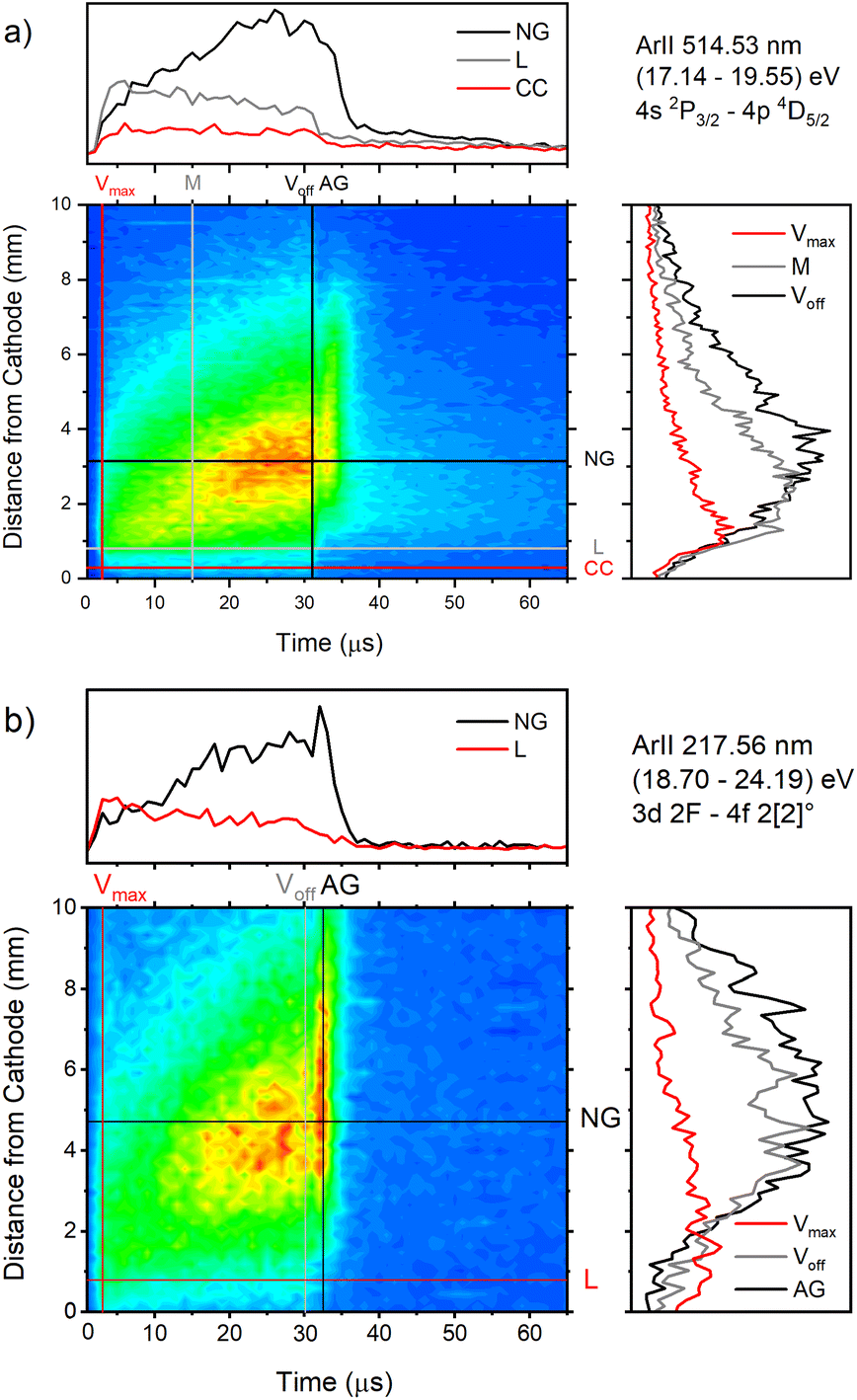 | ||
| Fig. 9 Spatio-temporal distribution of Ar II 514.53 nm (a) and Ar II 217.56 nm (b) spectral line (U = 880 V, I = 60 mA, P = 6 mbar, f = 5 kHz, pulse width = 30 μs). | ||
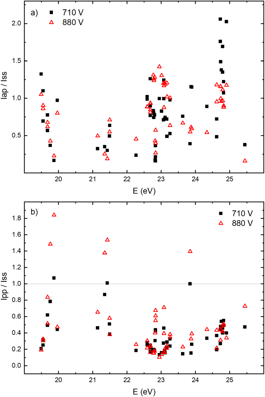
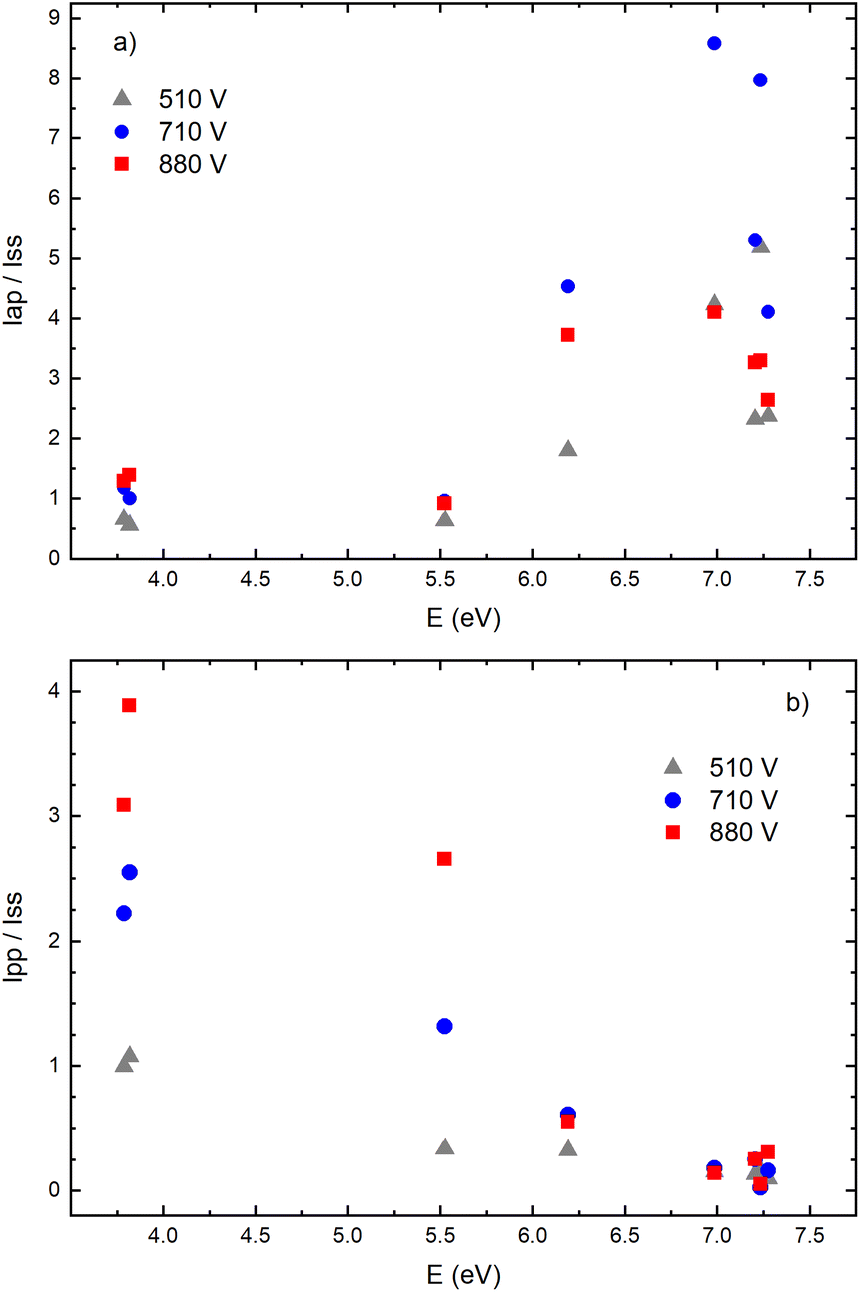
The appearance of the after-peak is observed for all recorded Ar II lines. Their intensities and decay times depend on the applied voltage and energy of the upper level. To understand after-peak behavior we need to mention that the highly excited states, formed in the recombination process relax to lower levels through collisional quenching and spontaneous emission. For the higher levels, the collisional quenching dominates, while for the lower levels the dominant process is de-excitation by emission. The both processes strongly depend on the quantum number40i.e. on the energy of the level. For comparison, the line intensity development for 50 Ar II lines, optical emission intensities were calculated by integration over the entire axial direction, to simulate end-on observation. Three characteristic intensities are used: Ipp – pre-peak intensity taken at maximum of intensity (local maximum) that arises at 3rd μs, Iss – steady-state intensity obtained at 30th μs, just before of the switching off the discharge, and Iap – maximal intensity in the afterglow i.e. after-peak intensity. The measured line intensities can be adequately compared only by using relative intensities i.e., ratios Ipp/Iss and Iap/Iss. Analyzing Fig. 10a one can conclude that the intensity ratio Iap/Iss show tendency of increase with the energy of the upper level, and that the increase is more evident for the lower voltage (i.e. lower electron energy and electron density). For the energy levels in the range 24.6–24.9 eV, Iap/Iss noticeably decreases with the voltage (current) increasing. An explanation of this behavior could be as follow: The voltage increasing in the Grimm discharge causes electron number density increasing36,41 that causes the increasing of collisional quenching of the argon ion's levels and consequently the decreasing of spontaneous emission.40 On the other side, increasing of the applied voltage increases Iap/Iss for the levels around 23 eV, see Fig. 10a, showing that processes of the dominant radiative de-excitation (Iap/Iss = 1.2–1.4) are moving towards the lower energy levels.
 | ||
| Fig. 10 Relative intensities dependence of energy level of Ar II spectral lines for two different applied voltages on μs-PDG (I = 40 mA, U = 710 V and I = 60 mA, U = 880 V) for ratios (a) Iap/Iss and (b) Ipp/Iss (P = 6 mbar, f = 5 kHz, pulse width = 30 μs). | ||
Fig. 10b shows that for the higher voltage, Ipp/Iss decreases with the increasing of the energy level and that the ratio is, in general, larger for the higher voltage. For some transitions Ipp is higher than Iss and for these transitions increasing of the voltage causes the largest increase of the ratio, see Fig. 10b. All these transitions are from 4p to 4s levels.
The decay time of the Ar II line intensity after the after-peak are shorter for the higher voltage for almost all recorded lines, see Fig. 11. A common characteristic of the Ar II line intensity in the afterglow is presented in Fig. 11b where one can see that, for the higher voltage, the after-peak of the Ar II 351.44 nm line appears earlier and the decays faster. Both decays cannot be interpreted as an exponential decrease of the line intensity and it seems that different processes are responsible for the decays,31 at least one before 40 and an another one after 50 microseconds.
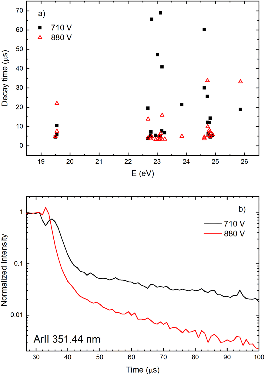 | ||
| Fig. 11 Decay time of the Ar II lines intensity after the after-peak (a) and normalized line intensity for after-peak in time for Ar II 351.44 nm spectral line (b) for two different applied voltages on μs-PDG I = 40 mA, U = 710 V and I = 60 mA, U = 880 V (P = 6 mbar, f = 5 kHz, pulse width = 30 μs). | ||
Temporal distributions of Ar II 217.6 nm and Ar II 514.5 nm lines have common shapes for the most of Ar II lines: the continual increase of the intensity during the discharge pulse. However, some of the Ar II lines have completely opposite behavior – fast increase of the intensity during the pre-peak time and then a continuous decrease, see for example Fig. 12. Their different behavior is characteristic for laser lines. In the field of ion laser plasma, a great effort has been made to understand excitation processes of Ar II lines, specifically the laser ones.42–44 Although the authors have been focused on the laser Ar II lines, the discussed excitation processes have a general character. The various electron-impact processes, which are connected with excitation or Ar II lines, are:
 | ||
| Fig. 12 Spatio-temporal distribution of Ar II 476.48 nm (a) and Ar II 487.99 nm (b) spectral line (U = 880 V, I = 60 mA, P = 6 mbar, f = 5 kHz, pulse width = 30 μs). | ||
1. Direct electron-impact excitation of the upper Ar II levels from the neutral atom ground state.
2. Electron-impact excitation from neutral metastable states.
3. Electron-impact excitation from the ion ground state.
4. Electron-impact excitation from metastable or long-lived states of the ion.
5. Excitation following radiative cascade from higher levels which are populated by one or more processes.
6. Recombination into excited states.
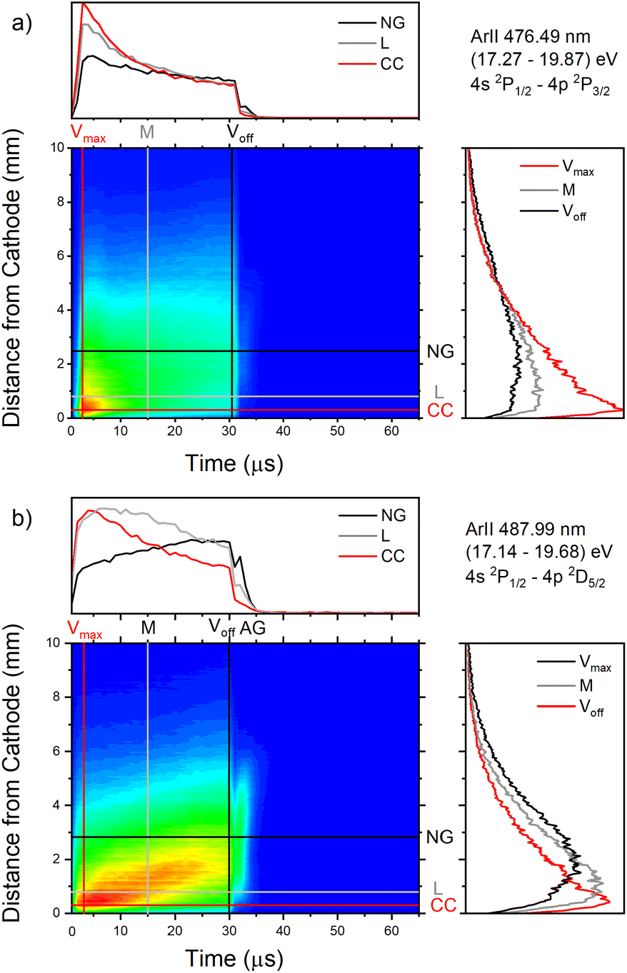
Only the first process is the single-step process, all the others are multi-step processes. The single-step electron-impact excitation was first suggested by Bennett et al.45,46 This process requires energetic electrons with energy >35 eV and/or exceptionally high E/P (higher than 1000 V cm−1 per Torr) and can only play a considerable role at low ionization degrees or high electron temperatures like in pulsed argon-ion lasers with pulse durations less than 1 μs. In our μs-PGD electrons have a quite high energy in the CF region and E/P is higher than 2000 V cm−1 per Torr at the position of the maximum of Ar II line intensity, see Fig. 12. Thus they could be excited in the single-step process. Among three intense laser lines Ar II 476.48 nm, Ar II 487.99 nm and Ar II 514.53 nm, the direct electron excitation is the most important process for the first one.46 Analyzing Fig. 12 one can see that the intensity of Ar II 476.5 nm line has a sharp maximum at the moment of maximal discharge voltage and after that it continuously decreases more steeply at the position close to the cathode. A similar profile to the mentioned one, but the profile of argon ion density distribution is predicted by the hybrid Monte Carlo fluid model for μs-PGD47 that has similar characteristics as our discharge. Additionally, the temporal development of the line intensity is similar to the signal of the argon ion, obtained by mass spectrometer in a PGD.48 The both profiles have a sudden increase (pre-peak) before decaying to a plateau i.e. to the steady-state condition, see Fig. 2 in (ref. 48) and Fig. 12a Ar II 476.48 nm spectral line. The fact that temporal dependence of the number of ions and the temporal dependence of the ion line intensity have similar shapes are consequence of the single-step processes – ionization, in the case of ion number measurement, and ionization with simultaneous ion excitation, for the line intensity. The shape of the obtained line intensity behavior can be explained as follows. At the beginning of the current pulse, the direct excitation of the upper laser level (35.5 eV above the neutral ground state) takes place, provided the mean electron energy is high enough. This energy rises with the E/P ratio, therefore the direct excitation is more pronounced at position closer to the cathode where the electric field has the higher value (see CC, L and NG profiles in Fig. 12). During the later time, two facts obstruct direct excitation: the neutral density is reduced by ionization, and the mean electron energy decreases, because the energy loss by elastic Coulomb collisions with ions is greater than by collisions with neutral atoms.49 Because of the decrease in number of direct excitations, the spontaneous emission drops. Meanwhile the density of ion ground or metastable states has become high enough to favor two- or multi-step excitation processes (processes 2–6). The total excitation rate rises, if the increase of two-step process (and possibly cascades from higher lying levels) compensates the decrease of the one-step process. In the case of Ar II 476.5 nm line (and several others 4s–4p transitions), the total excitation rate decreases after the pre-peak which means that dominant excitation process is the direct electronic excitation from the ground state of the atom. For Ar II 487.99 nm line the direct excitation is important only in the CF region where the electron energy is higher, while in the NG region, the two- and/or multi-step processes are more favor. Finally, Fig. 9a shows that Ar II 514.5 nm line is excited dominantly by two- and/or multi-step processes. It is expected since this line is known as the laser line whose major contribution is from the cascade excitation.46
Excitation from the neutral metastable states is less efficient than the previous one because the neutral metastable density in μs-PGD is about three orders of magnitude lower than atom number density.14
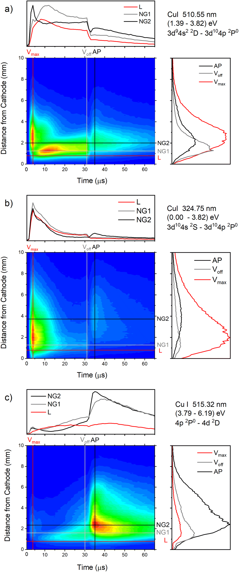 | ||
| Fig. 13 Spatio-temporal distribution of Cu I 510.55 nm (a), Cu I 324.75 nm (b) and Cu I 515.32 nm (c) spectral line (U = 880 V, I = 60 mA, P = 6 mbar, f = 5 kHz, pulse width = 30 μs). | ||
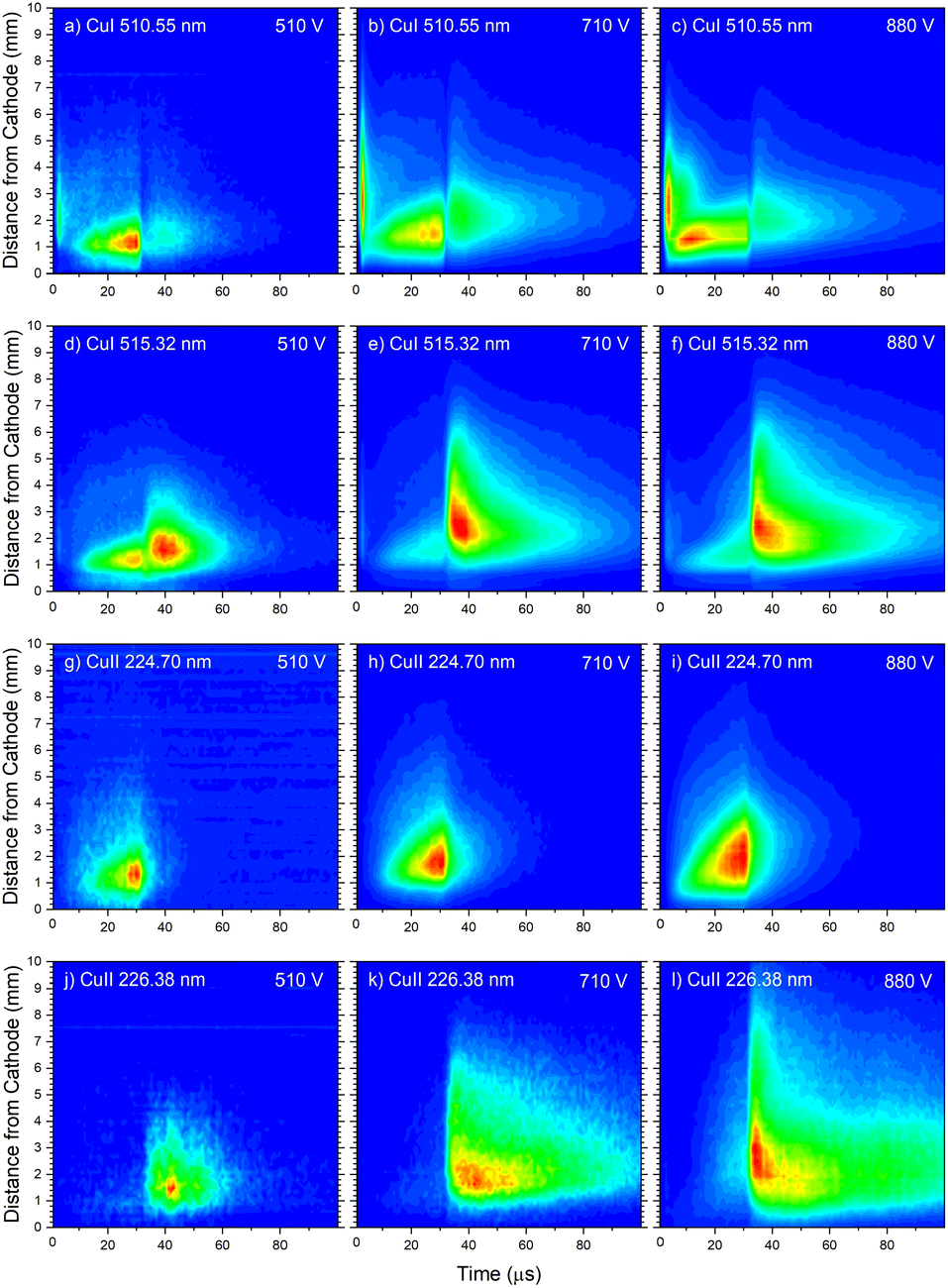 | ||
| Fig. 14 Spatio-temporal distribution of Cu I 510.55 nm (a–c), Cu I 515.32 nm (d–f), Cu II 224.70 nm (g–i) and Cu II 226.38 nm (j–l) spectral line for different voltages U = 510 V and I = 20 mA, U = 710 V and I = 40 mA, U = 880 V and I = 60 mA (P = 6 mbar, f = 5 kHz, pulse width = 30 μs). | ||
In the afterglow regime, Cu I 324.75 nm and Cu I 510.55 nm line have after-peaks at ∼4 μs after the discharge is switched off, see Fig. 13b and c. The after-peaks are located in the NG region: for Cu I 324.75 nm line at distance of ∼3.8 mm, while for Cu I 510.55 nm line at the distance of ∼2 mm. The after-peak of Cu I 510.55 nm line appears 9 μs after the switching off the discharge, and with increasing the voltage it appears earlier, after 6 μs and 5 μs for the voltages of 710 and 880 V, respectively, see Fig. 14a–c.
The Cu I 515.32 nm line has the lower energy level close to the higher level of the Cu I 510.55 nm line, see Fig. 5b. Analyzing Fig. 13c one can see that the Cu I 515.32 nm line intensity is much higher during the afterglow than during the pulse phase of the discharge. The line has a small pre-peak with a broad maximum located 1.7 mm away from the cathode. During the steady state phase, the line intensity increases with the time at all positions along the discharge, see Fig. 13c. As the self-absorption is excluded for this line, increasing of the line intensity with time is evidence of increasing of the copper atom number during the steady-state phase. During the afterglow phase the line intensity greatly increases at the distances that belongs to the NG region (during the active phase of the discharge); farther from the cathode the increasing is higher. Position of the afterpeak is located at ∼2.5 mm from the cathode and it remains unchanged during the afterglow development.
Increasing of voltages (currents) causes moving of the position of the maximal Cu I 515.32 nm line intensity away from the cathode (1.5, 2.4 and 2.6 mm) and appearance of the afterpeak earlier in the afterglow (∼9, 4 and 4 μs), see Fig. 14d–f.
Fig. 14a–f give examples of very different spatio-temporal intensity distributions for the two Cu I emission lines for different voltages. The distributions show that the afterpeak greatly increases with increasing energy of the upper level. On the opposite, the pre-peak emission intensity decreases with the increase of the energy of the upper level. In order to better understand the influence of the upper energy level on the line intensity development and to bring a quantitative description on this influence, the two graphs are presented in Fig. 15. Fig. 15b shows the ratio Ipp/Issvs. energy of the upper level for eight Cu I lines (578.21, 510.55, 224.43, 515.32, 221.46, 222.78, 221.57 and 219.97 nm) and three applied voltages (currents). Increasing of the applied voltage leads to an increase in the absolute intensity of the pre-peak (also observed in (ref. 13)), what is expected, because the copper line intensities increase with increasing of the voltage.54 It has been noticed (in the discharge similar to our) that the pre-peak of the highest relative line intensity (i.e. Ipp/Iss) is observed for the atomic copper lines with upper levels of relatively low energy.13 Analyzing the graph, one can conclude the same i.e., that Ipp/Iss decreases with increasing energy of the upper level, and that it is valid for all applied voltages. For the higher voltage the decreasing is steeper. The influence of the applied voltage on the relative intensity seems negligible for lines with the highest energy levels.
 | ||
| Fig. 15 Relative intensities dependence of energy level of Cu I spectral lines for three different applied voltages on μs-PDG (I = 20 mA, U = 510 V; I = 40 mA, U = 710 V; and I = 60 mA, U = 880 V) for ratios (a) Iap/Iss, (b) Ipp/Iss (P = 6 mbar, f = 5 kHz, pulse width = 30 μs). Dash lines are rough linear fits just used to show general trend. | ||
On the other side, the intensity of the after-peak has the opposite dependance on the energy of the upper level i.e. Iap/Iss increases with the energy increase, see Fig. 15a. This graph clearly shows that emission originating from higher upper levels is favored during the afterglow regime and that means that the excited states are populating from above during the recombination processes.30 Analyzing the graph one can notice that, for the energy higher than ∼6 eV, Iap/Iss ratio for 710 V (40 mA) is larger than the one for 880 V (60 mA), although the Iap intensities have opposite behavior. A plausible explanation of such results is based on nonradiative deexcitation processes that could be caused by copper atoms and electrons, particles whose concentrations increase with increase of current (voltage).
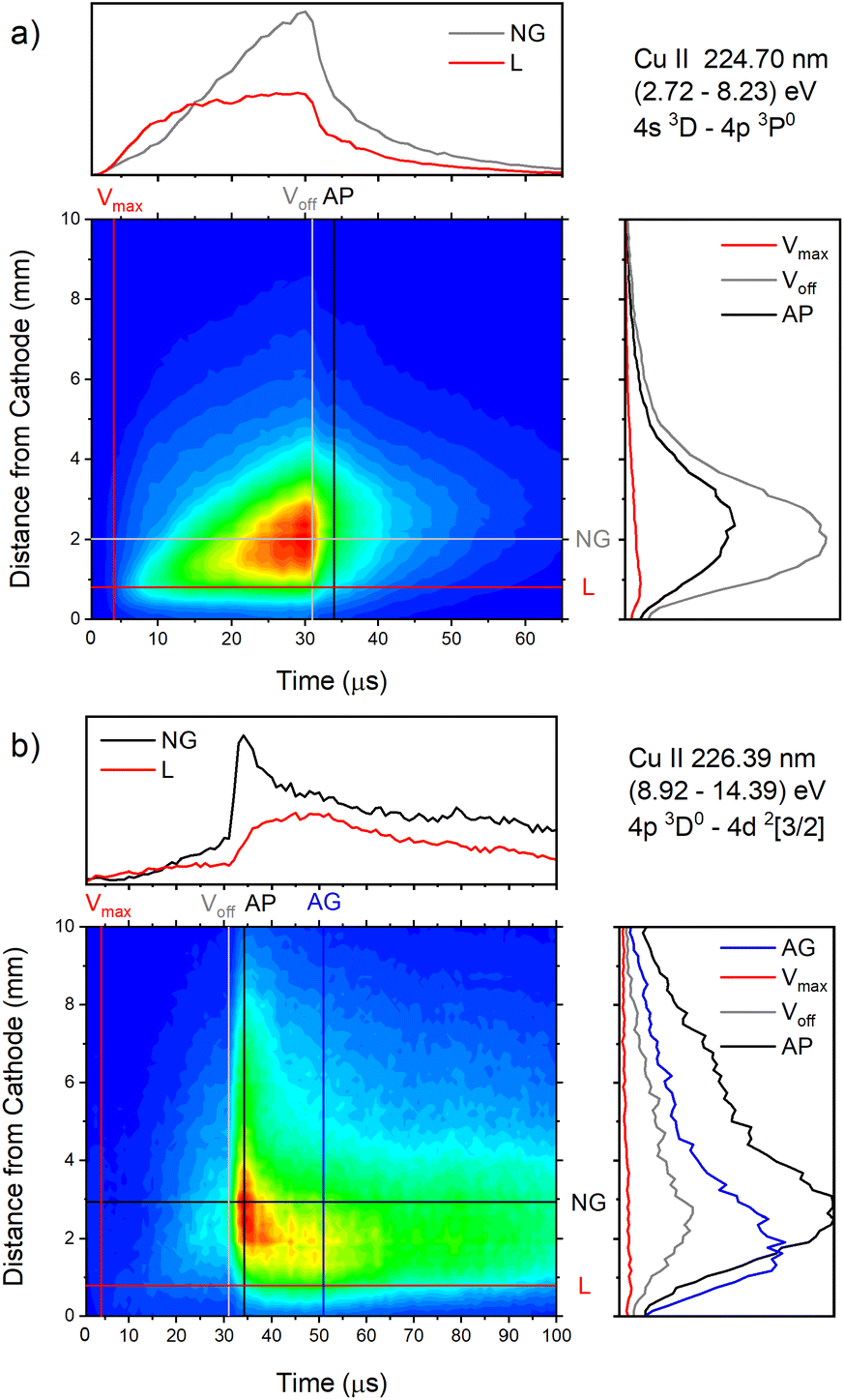 | ||
| Fig. 16 Spatio-temporal distribution of (a) Cu II 224.70 nm and (b) Cu II 226.38 nm spectral line (U = 880 V, I = 60 mA, P = 6 mbar, f = 5 kHz, pulse width = 30 μs). | ||
Analyzing Fig. 16a one can notice that, during the first 15 μs, intensity of the line emitted from the end of the CF region increases faster than the one emitted from the NG region, while for the rest time of the discharge pulse, the line intensity increasing has the opposite trend. This can be explained by the diffusion of the copper atoms from the cathode. Also, the diffusion explains why, during the discharge development, the maximum of the line intensity distribution moves away from the cathode. During the afterglow time, no after-peak behavior was observed, just exponential decrease of the line intensity, see Fig. 16a. Position of the maximum of the line intensity distribution at the end of the discharge pulse and in the afterglow differ from each other, what could be expected, since, during the discharge, the line is caused by the charge exchange of the copper atoms – Cu0, while in the afterglow, by a recombination of a copper ions – Cu2+. Spatio-temporal plots of the line intensity for three different voltages, are presented at Fig. 14g–i. For all used voltages, maximal values of the line intensity are obtained at the end of the discharge pulse, at increasing positions from the cathode of 1.3, 1.6 and 2.0 mm for 510, 710 and 880 V, respectively.
Cu II 226.38 nm line has a completely different behavior in comparison with Cu II 224.7 nm line; low intensity during the discharge pulse and much higher intensity in the afterglow, see Fig. 16b. Regardless of much lower line intensity during the discharge pulse, Cu II 226.38 nm line has very similar behavior as Cu II 224.70 nm line – faster increase of the intensity in the CF than in NG region during the first 15 μs, and opposite trend for the rest time of the discharge pulse. Also, position of the maximum of Cu II 226.38 nm line intensity at the end of the discharge pulse, as for Cu II 224.70 nm line, is closer to the cathode than the maximum intensity in the afterglow. The principal difference between the intensity of the Cu II 224.70 nm and the Cu II 226.38 nm lines is that the latter has a strong afterpeak. Position of the afterpeak is farther from the maximum line intensity obtained at the end of the discharge pulse, see Fig. 16b. The position of the afterpeak is moving from 2.9 to ∼2.3 mm during the afterglow development. Maximal value of the afterpeak is established ∼3 μs after the discharge pulse. Analogously as for Ar2+ ions, the afterglow of a Cu II line arises as a consequence of recombination of Cu2+ ion with electron in a process of three-body recombination. Comparing widths of the after-peaks, see Fig. 13c and 16b, one can see that the width of Cu I 515.32 nm line after-peak is larger than the width of Cu II 226.38 nm line after-peak. We couldn't find data for Cu2+ mobility, but it seems reasonable that, according to the after-peak widths, it is larger than the Cu+ mobility, similar as it is noticed for Ar2+ and Ar+ mobility.
Increasing voltages (510, 710 and 880 V) causes moving of position of maximal line intensity away from the cathode (1.5, 1.9 and 2.6 mm) and appearing the afterpeak earlier in the afterglow (∼11, 6 and 3 μs), see Fig. 14j–l. As the increase of the voltage causes the increasing of electron density and consequently increasing of collision frequency in three-body recombination processes, it is reasonable to expect that the afterpeak occurs earlier when voltage increases.
4 Conclusions
Here are presented experimental results of the spatio-temporal dynamics of the microsecond pulsed glow discharge (μPGD) of Grimm-type in argon, that works in abnormal glow regime. The high current peak observed during the discharge ignition is the most due to the capacitive displacement current, so modeling of the pulsed glow discharge must have that into account. Using Stark polarization spectroscopy of Hβ line, electric field distribution inside the μPGD is measured and the border between the cathode fall region (CFR) and the negative glow (NG) is determined. The electron excitation temperature of argon atoms and argon ions, measured at several distances from the cathode, slowly increases during the discharge development, getting the values of 0.5–1.0 eV for the atoms, and 1.4–1.7 eV for the ions. Spatio-temporal dynamics of selected spectral lines of atoms and ions of argon and copper were measured and analyzed during the three phase of the discharge evolution (pre-peak, steady-state and afterglow) and in the two regions (CFR and NG). The spectral lines of the mentioned species are selected in such a way that upper level of one line is close to the lower level of the other line. Such selected lines have different behavior during the pre-peak and the afterglow of the discharge. Usually, the lines with low energy upper level get the maximum intensity at the pre-peak time, while the lines with high energy upper level get the maximal intensity at the after-glow time. The time of appearing the afterpeak maxima for Ar I, Ar II, Cu I and Cu II lines decrease with the discharge voltage increase, showing that the recombination processes, responsible for the afterpeaks, are accelerated with increasing of ion and electron densities. Afterpeak appearances are earlier for Ar II lines than for Ar I lines because of higher mobility of Ar2+ than of Ar+ and consequently faster recombination. Also decay time for the Ar II afterpeaks are shorter than for the Ar I ones. Spatio-temporal dynamics of the argon lasers lines clearly show that intensity of Ar II 476.48 nm and Ar II 487.99 nm lines are caused by one and multistep excitation process, respectively. For Cu I and Cu II lines systematic differences in the afterpeak appearance haven't noticed, but the decay time of the Cu II lines intensities are shorter than for the Cu I lines. Spatio-temporal dynamics of resonant Cu I lines shows that they are self-absorbed during the steady-state phase of the discharge for all the used voltages, while the Cu I lines with the metastable lower level are partially self-absorbed only for the highest voltage. At the highest discharge voltage, electron density reaches a such value that, during the afterglow, deexcitation processes of the higher energy levels, caused by collisions with electrons, decreases relative line intensity (the after-peak divided by the steady-state intensity) of Ar II and Cu I lines. All the measurements and analyses presented here can be used for making a more precise model of the microsecond pulse glow discharge. Additionally, we hope that the analyses of the spectral lines of the sputtered material may be useful for the selection of proper lines (recorded in pre-peak or afterglow regime) and discharge conditions for the accurate analytical measurements.Conflicts of interest
There are no conflicts to declare.Acknowledgements
This research was supported by the Ministry of Science, Technological Development and Innovation of the Republic of Serbia [451-03-47/2023-01/200162]. The authors would like to thank Goran Sretenović for his constructive advices during the writing of this paper.References
- P. Belenguer, M. Ganciu, P. Guillot and T. Nelis, Spectrochim. Acta, Part B, 2009, 64, 623–641 CrossRef.
- P. Subramonium and M. J. Kushner, J. Vac. Sci. Technol., A, 2002, 20, 313–324 CrossRef CAS.
- A. Anders, Surf. Coat. Technol., 2004, 183, 301–311 CrossRef CAS.
- S.-H. Song, M. D. Logue, Y. Zhang, P. Tian and M. J. Kushner, ESCAMPIG XXI, Viana do Castelo, Portugal, 2012 Search PubMed.
- S. Samukawa and S. Furuoya, Appl. Phys. Lett., 1993, 63, 2044–2046 CrossRef CAS.
- Y. Watanabe, M. Shiratani, Y. Kubo, I. Ogawa and S. Ogi, Appl. Phys. Lett., 1988, 53, 1263–1265 CrossRef CAS.
- W. W. Harrison, W. Hang, X. Yan, K. Ingeneri and C. Schilling, J. Anal. At. Spectrom., 1997, 12, 891–896 RSC.
- M. Voronov and V. Hoffmann, J. Anal. At. Spectrom., 2018, 33, 663–669 RSC.
- M. Voronov, V. Hoffmann, W. Buscher, C. Engelhard, S. J. Ray and G. M. Hieftje, J. Anal. At. Spectrom., 2012, 27, 1225 RSC.
- W. Grimm, Spectrochim. Acta, Part B, 1968, 23, 443–454 CrossRef CAS.
- M. K. Levy, D. Serxner, A. D. Angstadt, R. L. Smith and K. R. Hess, Spectrochim. Acta, Part B, 1991, 46, 253–267 CrossRef.
- M. Kuraica and N. Konjević, Phys. Rev. A, 1992, 46, 4429–4432 CrossRef CAS PubMed.
- M. Voronov and V. Hoffmann, Anal. Bioanal. Chem., 2014, 406, 7445–7454 CrossRef CAS PubMed.
- A. Bogaerts and R. Gijbels, J. Anal. At. Spectrom., 2001, 16, 239–249 RSC.
- D. Alberts, P. Horvath, T. Nelis, R. Pereiro, N. Bordel, J. Michler and A. Sanz-Medel, Spectrochim. Acta, Part B, 2010, 65, 533–541 CrossRef.
- G. Gamez, A. Bogaerts and G. M. Hieftje, J. Anal. At. Spectrom., 2006, 21, 350 RSC.
- A. Bengtson, C. Yang and W. W. Harrison, J. Anal. At. Spectrom., 2000, 15, 1279–1284 RSC.
- C. Yang, E. Oxley and W. W. Harrison, J. Anal. At. Spectrom., 2001, 16, 1131–1134 RSC.
- V. Efimova, V. Hoffmann and J. Eckert, J. Anal. At. Spectrom., 2011, 26, 784–791 RSC.
- A. Bogaerts and R. Gijbels, J. Anal. At. Spectrom., 2000, 15, 441–449 RSC.
- I. R. Videnović, N. Konjevic and M. M. Kuraica, Spectrochim. Acta, Part B, 1996, 51, 1707–1731 CrossRef.
- Z. Wroński, Vacuum, 1990, 40, 387–394 CrossRef.
- Z. Wronski, S. Saied, C. Pearce and J. Sullivan, Vacuum, 1993, 44, 1161–1169 CrossRef CAS.
- A. Martín, N. Bordel, R. Pereiro and A. Bogaerts, Spectrochim. Acta, Part B, 2008, 63, 1274–1282 CrossRef.
- A. Kramida, Y. Ralchenko, J. Reader and The NIST ASD Team (2018), NIST Atomic Spectra Database (Ver. 5.6.1), National Institute of Standards and Technology, Gaithersburg, MD, 2019 Search PubMed.
- E. L. Bydder and G. P. Miller, Spectrochim. Acta, Part B, 1988, 43, 819–829 CrossRef.
- G. P. Jackson and F. L. King, Spectrochim. Acta, Part B, 2003, 58, 1417–1433 CrossRef.
- B. M. Jelenković and A. V. Phelps, J. Appl. Phys., 1999, 85, 7089–7096 CrossRef.
- S. Ashida, M. R. Shim and M. A. Lieberman, J. Vac. Sci. Technol., A, 1996, 14, 391–397 CrossRef CAS.
- C. L. Lewis, G. P. Jackson, S. K. Doorn, V. Majidi and F. L. King, Spectrochim. Acta, Part B, 2001, 56, 487–501 CrossRef.
- X. Yan, Y. Lin, R. Huang, W. Hang and W. W. Harrison, J. Anal. At. Spectrom., 2010, 25, 534 RSC.
- G. P. Jackson and F. L. King, Spectrochim. Acta, Part B, 2003, 58, 185–209 CrossRef.
- A. Bogaerts, Z. Donko, K. Kutasi, G. Bano, N. Pinhao and M. Pinheiro, Spectrochim. Acta, Part B, 2000, 55, 1465–1479 CrossRef.
- A. Bogaerts and R. Gijbels, Spectrochim. Acta, Part B, 2000, 55, 263–278 CrossRef.
- A. Bogaerts, J. Anal. At. Spectrom., 2007, 22, 502–512 RSC.
- A. Bogaerts, R. Gijbels, G. Gamez and G. M. Hieftje, Spectrochim. Acta, Part B, 2004, 59, 449–460 CrossRef.
- L. A. Viehland and E. A. Mason, At. Data Nucl. Data Tables, 1995, 60, 37–95 CrossRef CAS.
- X. Yan, K. Ingeneri, W. Hang and W. W. Harrison, J. Anal. At. Spectrom., 2001, 16, 819–824 RSC.
- B. Clarenbach, B. Lorenz, M. Krämer and N. Sadeghi, Plasma Sources Sci. Technol., 2003, 12, 345–357 CrossRef CAS.
- Y. Celik, T. V. Tsankov, M. Aramaki, S. Yoshimura, D. Luggenhölscher and U. Czarnetzki, Phys. Rev. E: Stat., Nonlinear, Soft Matter Phys., 2012, 85, 1–12 Search PubMed.
- A. Bogaerts and R. Gijbels, Spectrochim. Acta, Part B, 1998, 53, 437–462 CrossRef.
- W. B. Bridges, A. N. Chester, J. V. Parker and A. S. Halsted, Proc. IEEE, 1971, 59, 724–737 CAS.
- J. Jolly, J. Quant. Spectrosc. Radiat. Transfer, 1978, 20, 503–518 CrossRef CAS.
- V. F. Kitaeva, A. N. Odintsov and N. N. Sobolev, Phys.-Usp., 1970, 12, 699–730 CrossRef.
- W. R. Bennett, J. W. Knutson, G. N. Mercer and J. L. Detch, Appl. Phys. Lett., 1964, 4, 180–182 CrossRef CAS.
- W. R. Bennett, G. N. Mercer, P. J. Kindlmann, B. Wexler and H. Hyman, Phys. Rev. Lett., 1966, 17, 987–991 CrossRef CAS.
- A. Bogaerts and R. Gijbels, J. Anal. At. Spectrom., 2000, 15, 895–905 RSC.
- J. A. Klingler, C. M. Barshick and W. W. Harrison, Anal. Chem., 1991, 63, 2571–2576 CrossRef CAS.
- W. Demtröder, Phys. Lett., 1966, 22, 436–438 CrossRef.
- P. A. Bokhan and V. I. Solomonov, Quantum Electron., 1974, 3, 481–483 Search PubMed.
- A. Bogaerts, R. Gijbels and R. J. Carman, Spectrochim. Acta, Part B, 1998, 53, 1679–1703 CrossRef.
- H.-L. Chen and G. Erbert, J. Chem. Phys., 1983, 78, 4985–4990 CrossRef CAS.
- T. Nelis, M. Aeberhard, M. Hohl, L. Rohr and J. Michler, J. Anal. At. Spectrom., 2006, 21, 112–125 RSC.
- A. Bogaerts and R. Gijbels, J. Anal. At. Spectrom., 1998, 13, 721–726 RSC.
- E. B. M. Steers and R. J. Fielding, J. Anal. At. Spectrom., 1987, 2, 239–244 RSC.
- I. Krstić, B. Obradović and M. Kuraica, J. Instrum., 2020, 15, C01006 CrossRef.
| This journal is © The Royal Society of Chemistry 2024 |