
 Open Access Article
 This Open Access Article is licensed under a
 Creative Commons Attribution 3.0 Unported Licence
Precise control of process parameters for >23% efficiency perovskite solar cells in ambient air using an automated device acceleration platform†
Jiyun
Zhang
 *ab,
Jianchang
Wu
ab,
Anastasia
Barabash
b,
Tian
Du
ab,
Shudi
Qiu
b,
Vincent M.
Le Corre
ab,
Yicheng
Zhao
c,
Kaicheng
Zhang
b,
Frederik
Schmitt
a,
Zijian
Peng
b,
Jingjing
Tian
b,
Chaohui
Li
b,
Chao
Liu
ab,
Thomas
Heumueller
ab,
Larry
Lüer
b,
Jens A.
Hauch
ab and
Christoph J.
Brabec
*ab
*ab,
Jianchang
Wu
ab,
Anastasia
Barabash
b,
Tian
Du
ab,
Shudi
Qiu
b,
Vincent M.
Le Corre
ab,
Yicheng
Zhao
c,
Kaicheng
Zhang
b,
Frederik
Schmitt
a,
Zijian
Peng
b,
Jingjing
Tian
b,
Chaohui
Li
b,
Chao
Liu
ab,
Thomas
Heumueller
ab,
Larry
Lüer
b,
Jens A.
Hauch
ab and
Christoph J.
Brabec
*ab
aForschungszentrum Jülich GmbH, Helmholtz-Institute Erlangen-Nürnberg (HI ERN), Department of High Throughput Methods in Photovoltaics, Immerwahrstraße 2, Erlangen 91058, Germany
bFriedrich-Alexander-University Erlangen-Nuremberg (FAU), Faculty of Engineering, Department of Material Science, Institute of Materials for Electronics and Energy Technology (i-MEET), Martensstrasse 7, Erlangen 91058, Germany. E-mail: jiyun.zhang@fau.de; christoph.brabec@fau.de
cUniversity of Electronic Science and Technology of China (UESTC), State Key Laboratory of Electronic Thin Films and Integrated Devices, School of Electronic Science and Engineering, Chengdu 611731, China
First published on 28th June 2024
Abstract
Achieving high-performance perovskite photovoltaics, especially in ambient air, is critically dependent on the precise optimization of process parameters. However, traditional manual methods often struggle to effectively control the key variables. This inherent challenge requires a paradigm shift toward automated platforms capable of precise and reproducible experiments. Herein, we use a fully automated device acceleration platform (DAP) to optimize air-processed parameters for preparing perovskite devices using a two-step sequential deposition technique. Over ten process parameters with significant potential to influence device performance are systematically optimized. Specifically, we delve into the impact of the dripping speed of organic ammonium halide, a parameter that is difficult to control manually, on both perovskite film and device performance. Through the targeted design of experiments, we reveal that the dripping speed significantly affects device performance primarily by adjusting the residual PbI2 content in the films. We find that optimal dripping speeds, such as 50 µL s−1, contribute to top-performance devices. Conversely, excessively fast or slow speeds result in devices with comparatively poorer performance and lower reproducibility. The optimized parameter set enables us to establish a standard operation procedure (SOP) for additive-free perovskite processing in ambient conditions, which yield devices with efficiencies surpassing 23%, satisfactory reproducibility, and state-of-the-art photo-thermal stability. This research underscores the importance of understanding the causality of process parameters in enhancing perovskite photovoltaic performance. Furthermore, our study highlights the pivotal role of automated platforms in discovering innovative workflows and accelerating the development of high-performing perovskite photovoltaic technologies.
Broader contextThe rapid advancement of emerging perovskite photovoltaic (PV) technology is a beacon of hope in the quest for efficient and cost-effective energy solutions. With the efficiency of perovskite-based devices soaring, the conventional fabrication process, confined to inert atmospheres (e.g., N2-filled glovebox), poses significant hurdles for large-scale production and cost reduction. The necessity to shift towards air-based fabrication methods is palpable. However, the journey is fraught with challenges, particularly the precise control of critical process variables, and is often hampered by the limitations of manual optimization reliant on operator expertise. Here, we introduce an air-based perovskite devices manufacturing protocol, which harnesses the potential of an automated device acceleration platform (DAP) to transcend the constraints of traditional methods. By leveraging the automation platform, we embark on a methodical exploration of process parameters, culminating in the optimization of fabrication technique that yields high-efficiency additive-free perovskite devices with exceptional reproducibility and stability under ambient conditions. |
Introduction
Emerging perovskite photovoltaics have become a revolutionary next-generation technology in the renewable energy field, providing unprecedented opportunities for efficient and affordable solar power generation.1–3 At the core of this advancement is the pursuit of high-performance perovskite photovoltaic technology, which is essential to unlock the full potential and maximize the capabilities of this promising technology.4,5 The fabrication of high-performance perovskite devices usually requires an inert atmosphere (for instance a nitrogen-filled glovebox),6,7 which dramatically reduces scalability due to higher preparation costs, limited production scale, and more complicated preparation processes.8,9 Therefore, the preparation of high-performance perovskite solar cells (PSCs) in ambient air is expected to overcome these challenges. The realization of high-performance PSCs in ambient air is closely related to the precise control and optimization of various manufacturing process parameters that govern the quality of the perovskite film and device fabrication.10,11 Hence, the optimal selection of process parameters has become a key factor affecting the efficiency and stability of perovskite photovoltaic cells.12However, traditional manual methods encounter huge challenges in effectively controlling key variables as they are frequently limited by the skills and experience of the operators.13,14 These challenges are exacerbated by the rapid crystallization dynamics of perovskites, significantly adding complexity to the fabrication process in addition to the intricate interdependence of factors affecting device performance. As nucleation and crystal growth occur on the sub-second timescale and strongly depend on preconditions (e.g., solvent-/gas-quenching), manual operations are finding their limits in achieving highly reproducible outcomes upon mass production.15,16 To overcome the limitations of manual optimization methods and unlock the full potential of perovskite photovoltaics fabricated in ambient air, there is an increasingly urgent need for a paradigm shift toward innovative technologies that enable more precise and reproducible experiments.
Automated material and device acceleration platforms (MAPs and DAPs) have emerged as transformative tools across various scientific fields, promoting breakthroughs and efficiency improvements through high-throughput experiments and systematic exploration.17–21 The main advantage of these automated platforms is their capability to perform experiments with unprecedented efficiency and reproducibility.22 By automating repetitive tasks and minimizing human intervention, these platforms ensure a FAIR data integrity as well as the highest reliability.23–25 With exceptional precision, speed, and accuracy, automated platforms have achieved remarkable success in accelerating research in areas like organic synthesis, drug discovery, and biology technology.26–31 The methodology of integrating automation in energy thin film materials research, especially solution-processed perovskite photovoltaics materials, has attracted widespread attention.10,32–36 Compared to traditional manual methods, DAPs are specifically promising for perovskite photovoltaics manufacturing where rather small inconsistencies in the process can cause significant deviation in the batch-to-batch performance.37 We believe that the introduction of automated manufacturing systems in perovskite photovoltaics research holds great potential for overcoming long-standing challenges associated with manual manufacturing methods.
In this study, we utilize an automated DAP named SPINBOT to optimize process parameters for fabricating full perovskite devices in ambient air. The process parameters that significantly affect device performance were systematically optimized using the one-variable-at-a-time (OVAT) method. Specifically, the influence of the dripping speed of organic ammonium halide on both perovskite film and device performance was finely studied. The results demonstrate that moderate dripping speeds (e.g., 50 µL s−1) are most advisable for producing top-performing devices, whereas too fast or slow speeds would result in samples with relatively poorer performance and uneven outcomes. By optimizing the parameter set, we finally achieved perovskite devices processed under ambient conditions with a champion efficiency exceeding 23%. Furthermore, the devices from optimized parameters demonstrated excellent reproducibility and state-of-the-art photo-thermal stability, retaining 93% ± 3% of their initial efficiency after 1200 hours of continuous aging. This study highlights not only the significance of precise process parameter optimization for enhancing perovskite photovoltaic performance but also demonstrates the critical role of automated platforms in streamlining experimental workflows and accelerating high-performance perovskite photovoltaics development.
Results and discussion
Fig. 1A illustrates the automated fabrication procedure for solution-processed PSCs with a structure of ITO/SnO2/Perovskite/Spiro-OMeTAD/Au (Fig. 1B) using the two-step sequential deposition technique in ambient air. Specifically, a wet PbI2/CsI layer is formed by depositing the PbI2/CsI precursor onto a SnO2-coated ITO substrate without annealing.38 In the next step, the organic ammonium halide solution is dynamically drop-cast onto the wet PbI2/CsI film. After spin-drying the layer, the substrate is then annealed in the air. The final spin-coating step involves the deposition of spiro-OMeTAD solution as the hole-transporting layer. All the above solution-processed layers are formed through the SPINBOT platform in the air environment. The streamlined fabrication process of thin layers can be found in the ESI† Video.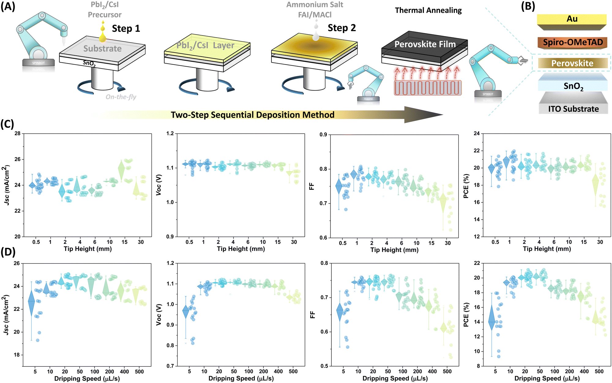 | ||
| Fig. 1 Schematic of automated fabrication and statistical performance of perovskite devices. (A) Schematic of the autonomous fabrication process for perovskite films using the two-step sequential deposition method. (B) The architecture of PSCs (ITO/SnO2/perovskite/Spiro-OMeTAD/Au). (C) Grouped performance statistics for perovskite devices fabricated with different pipette tip heights at the drip of FAI/MACl solution. The tip heights are 0.5, 1, 2, 4, 6, 10, 15, and 30 mm, respectively. (D) Statistical performance of the perovskite devices as a function of the dripping speed of the ammonium halide. The drip speeds are 5, 10, 20, 50, 100, 200, 400, and 500 µL s−1, respectively. | ||
To evaluate the influence of process parameters on device performance, a comprehensive parameter list of all process parameters was first compiled, as illustrated in Fig. S1 (ESI†). Based on the preliminary review and analysis of various process parameters that potentially affect device performance, over ten individual and combination parameters, such as operational conditions, precursor volumes (Fig. S2, ESI†), spin speed combinations (Fig. S3, ESI†) and spin duration at different stages (Fig. S4 and S5, ESI†), were selected for in-depth study, as listed in Table 1. The process parameters were identified and optimized using the OVAT method. This approach allowed us to effectively isolate and analyze the impact of each parameter. To quantify the impact of individual process parameters on device performance, particularly efficiency, we introduced two indicators: relative efficiency potential and potential factor. Relative efficiency potential is defined as the normalized range of change in device efficiency from the minimum to the maximum within a given parameter optimization range. The potential factor further quantifies this change interval and is represented by calculating the difference between the minimum and maximum values of the normalized efficiency. This method allowed us to intuitively identify and evaluate the impact intensity of individual process parameters on device performance, thus revealing the key parameters that influence the final performance of the device. After experimental research and data analysis, the operational atmosphere, spin speed combinations, pipette tip height, and dripping speed of organic ammonium salt were identified as key parameters that significantly impact device performance. In the following section, their effects on the device/film are detailed.
| Input variable | Range (min–max) | Interval | Relative efficiency potential | Potential factor |
|---|---|---|---|---|
| Atmosphere (gas flow) | 0–5 bar | 1 bar | 9.0–75.2% | 0.662 |
| Spin speed S1 | 900–2500 rpm | 200 rpm | 43.0–93.9% | 0.509 |
| Spin speed S2 | 900–2500 rpm | 250 rpm | 43.0–93.9% | 0.509 |
| Spin duration t2 | 12–21 s | 3 s | 66.2–96.1% | 0.299 |
| Pipette tip height | 0.5–30 mm | 1 mm | 169.8–98.7% | 0.289 |
| Dripping speed | 5–500 µL s−1 | 5 µL s−1 | 30.6–94.8% | 0.642 |
| Spin duration t3 | 5–26 s | 3 s | 71.1–100% | 0.289 |
| Spiro-OMeTAD | Static/OTF (on-the-fly) | 82.1–92.8% | 0.107 | |
| Dispense mode | Dynamic | 77.4–91.1% | 0.137 | |
| Spin speed S3 | 3000–5000 rpm | 1000 rpm | 58.0–76.7% | 0.187 |
In the SPINBOT system, nitrogen gas flow is normally supplied into the mini-spin-coater bowel (Fig. S6, ESI†) for rapid removal of residual solvent vapor and the creation of a better-controlled atmosphere during the film deposition process.39 To investigate the influence of operational conditions on the device performance, different operational atmospheres were built by adjusting the airflow pressure. Fig. S7 (ESI†) presents the statistical performance distribution of perovskite devices fabricated under different operational atmospheres. The impact of nitrogen supply on device performance is evident. Samples processed without gas flow exhibit the poorest performance, with efficiencies ranging between 2–5%. This indicates that unregulated solvent accumulation within the spin-coater can dramatically impair the device's performance. However, there is a remarkable improvement in device performance with the introduction of fresh airflow. In particular, when the airflow pressure was set to 3 bar, the efficiency and uniformity of the devices reached the optimum level compared to other conditions. A notable advantage of the SPINBOT platform over manual process engineering is its capability to control typically unregulated parameters, such as the pipette tip height and ejection speed of the spin-coating dripping nozzle. Fig. 1C presents the grouped statistics illustrating the impact of various pipette tip heights during FAI/MACl dripping on the performance metrics of perovskite devices. The results suggest that relatively lower tip heights generally enhance the fill factor (FF) and PCE, while the short-circuit current density (Jsc) and open-circuit voltage (Voc) are less sensitive to changes in tip height. Specifically, Voc values remain relatively stable across a range of tip heights, which only show minor fluctuations at the maximum height of 30 mm. FF improves slightly as the tip height increases from 0.5 to 2 mm, then plateaus and gradually declines with further increases in tip height. Devices with a tip height of 30 mm exhibit significantly poorer performance and reproducibility, indicating that tip heights exceeding 15 mm during ammonium halide solution dripping can significantly impair device performance. Jsc values are relatively constant across varying tip heights, with a slight increase observed at higher heights. PCE improves markedly at a tip height of 1–2 mm, but efficiency gains level off or decrease slightly beyond this range. The optimal PCE is observed at a tip height of 1 mm, underscoring the importance of maintaining relatively lower tip heights during FAI/MACl dripping to achieve optimal device performance. Another critical parameter, the dripping speed of organic ammonium halide precursor, which was often overlooked in previous literature due to the huge challenges of manual control, can be more precisely regulated with the robotic platform. By fixing the dripping volume of the ammonium halide solution and varying the dripping speed in increments as small as 0.1 µL s−1 (ranging from 0.1 to 500 µL s−1), we were able to thoroughly investigate this aspect in perovskite processing. Here, the dripping speed refers to the ejection speed at which the ammonium halide solution is dispensed from the pipette tip onto the preformed PbI2/CsI layer during the spin-coating process. Fig. 1D presents the statistical performance distribution of perovskite devices as a function of ejection speeds (5, 10, 20, 50, 100, 200, 400, and 500 µL s−1, respectively) of ammonium halide. It is obvious that this parameter massively influences the performance behavior of the resulting devices, particularly the Jsc and FF. Generally, these performance metrics improve as the speed increases, but they gradually decline after reaching an optimum of around 20 to 50 µL s−1 with further acceleration. Deviations from this optimal range, either too fast or too slow speeds can lead to devices with relatively poorer performance and uncertain outcomes.
To investigate the underlying mechanism behind this phenomenon, the microstructural features of the films were first examined. Top-view scanning electron microscope (SEM) images in Fig. 2A and Fig. S8 and S9 (ESI†) illustrate the morphological variations observed in perovskite thin films. While all samples display compact and pinhole-free characteristics, noticeable differences in morphology are observed. The grain size distributions depicted in Fig. S10 (ESI†) demonstrate that increasing dripping speeds are correlated with noticeable increases in grain sizes. Specifically, the grain size averages are as follows: at a dripping speed of 5 µL s−1, the grains measure approximately 1.01 µm; increasing the speeds to 50 and 200 µL s−1 results in an average size of 1.3 and 1.81 µm, respectively; and at the highest speed of 500 µL s−1, the grains average 2.3 µm. Additionally, as the dripping speeds increase, there is a noticeable increase in the content of the white phase. Remarkably, when the speed exceeds 400 µL s−1, approximately half of the film surface is occupied by the white phase. Previous studies have linked the white phase to the PbI2 phase, while the black phases are associated with perovskite materials, indicating the predominant presence of the PbI2 phase along the grain boundaries of perovskites.40 This observation is further confirmed by X-ray diffraction (XRD) patterns presented in Fig. 2B, which demonstrate an escalating diffraction intensity of the PbI2 phase at 12.7° with higher dripping speeds. Conversely, the diffraction intensity of the primary perovskite phases around 14.0° exhibits an almost linear increase, reaching peak values within the speed range of 50 to 200 µL s−1, beyond which it declines with the further acceleration of the ejection speed, as depicted in Fig. 2C. Dripping speed markedly influences the thickness of the resulting films (Fig. S11, ESI†). As the dripping speed increases, there is a corresponding decrease in film thickness, ranging from approximately 860 nm to about 800 nm. Notably, this variation in thickness is more pronounced at relatively higher and lower dripping speeds.
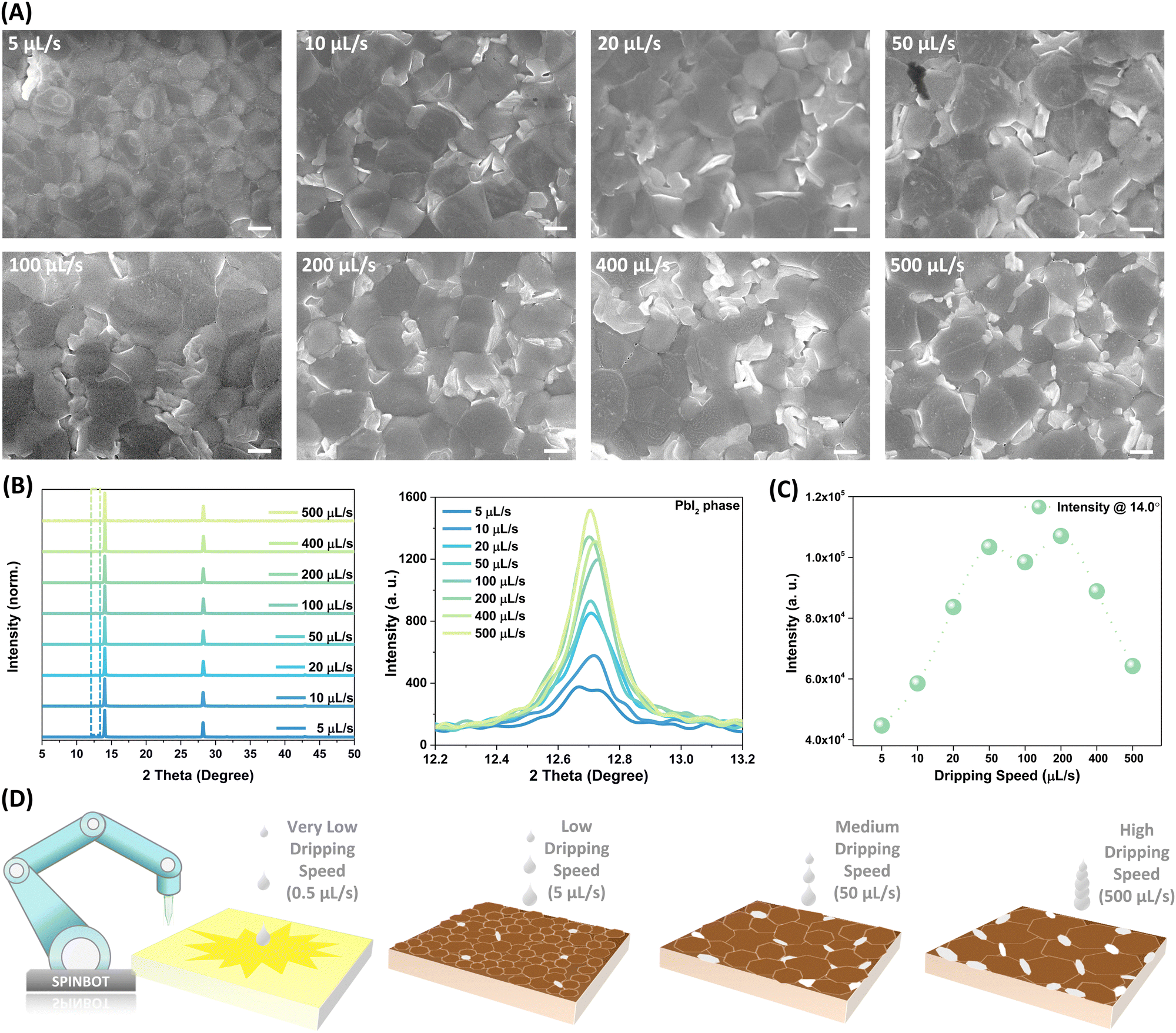 | ||
| Fig. 2 Structural characterizations and analysis of perovskite thin films. (A) Top-view SEM images (the scale bar is 1 µm), (B) XRD patterns and magnified view focused around 12.7° (corresponds to PbI2 phase), and (C) diffraction intensity of perovskite phase peaks (at 14°) of perovskite films fabricated with different dripping speeds of organic ammonium halide solution. (D) Schematic of the effect of varying dripping speeds on the morphology and crystallization of perovskite films. | ||
Driven by the significant impact of dripping speed on perovskite film and device performance, we further reduced the dripping speed to observe the resultant effects. As shown in Fig. S12 (ESI†), as the speeds decrease from 10 µL s−1 to 5, 4, 2, 1, and 0.5 µL s−1, the colors of samples change from completely black to yellowish during spin coating and the samples processes with slow dripping speeds cannot convert to black perovskite phase even after thermal annealing (Fig. 2D). The appearance of yellow phases at the film edges is observed at a speed of 5 µL s−1, their proportion increases at 4 µL s−1 ultimately resulting in a yellowish film at speeds below 2 µL s−1. These yellow non-perovskite phases are identified as PbI2–DMSO compounds through structural and in situ optoelectronic characterization (Fig. S13, ESI†).41 The lower ejection speed leads to a prolonged dripping interval. For example, at a speed of 2 µL s−1, dispensing a droplet of isopropanol (IPA) based precursor (approximately 6–7 µL) results in an interval of approximately 3–3.5 s. This extended duration poses challenges for the ammonium salts dissolved in volatile IPA solvent to quickly replace the DMSO molecules intercalated in the PbI2 phase beneath the surface through direct intramolecular exchange, while converting the perovskite partially on the top, thus hindering the complete generation of perovskite crystallization.42 The results indicate a critical minimum dripping speed for ammonium halide necessary for complete perovskite formation when employing the two-step deposition method (Fig. S14, ESI†). In our experiments, this threshold dripping speed is approximately 10 µL s−1 (the dropping interval is about 0.6 s).
The structural variations within the perovskite lattice result in diverse optoelectronic properties. Notably, the solution dripping speed significantly influences the bandgap and homogeneity of the films. As presented in Fig. 3A and Fig. S15 (ESI†), the sample prepared with the lowest dripping speed exhibits the smallest bandgap (∼1.55 eV), with the peaks gradually shifting towards a wider direction from 800.9 nm to 794.3 nm. The optical bandgap of PbI2 is larger than that of perovskite, which may cause the blue shift of the PL emission peak.43 PbI2 can form a type-I band alignment with perovskite,44,45 and excess PbI2 can passivate the surface or/and grain boundary of perovskite layers, which can enhance solar cell performance, particularly in terms of charge separation and collection.46–48 To evaluate film homogeneity, multiple positions (13 points) with regular patterns on each sample were characterized through a high-throughput spectrometer.49–51 The coefficient of variation (CV) of PL peak intensity extracted from these PL spectra (Fig. S16, ESI†) was calculated, as depicted in Fig. 3B. The CV value gradually decreases at a doubling rate as the ejection speeds increase (indicating better homogeneity), and maintains a relatively lower value range between 20 to 200 µL s−1. Conversely, continuous increases in dripping speed lead to a rapid decrease in film uniformity. A similar trend is observed for samples fabricated with different dripping volumes of organic ammonium halide precursor (Fig. S17, ESI†). To visually depict the evolution of homogeneity in the samples, PL intensity contour maps were plotted and presented in Fig. 3C. It is evident that relatively lower or higher dripping speeds significantly compromise film homogeneity, while films with satisfactory homogeneity are achieved within the speed range of 20 to 200 µL s−1. The conclusion is further evidenced by the UV-Vis absorption spectra of films prepared at various speeds (Fig. S18, ESI†). Fig. 3D and E present the in situ PL spectra of wet perovskite films fabricated with fast (>50 µL s−1) and slow (∼0.5 µL s−1) dripping speeds, respectively. Obviously, faster dripping speed facilitates the rapid formation of the perovskite phase, resulting in strong and continuous PL signals. In contrast, the film fabricated with relatively slower dripping speeds shows weaker perovskite signals, with emission signals that gradually blue-shifted and decreased in intensity. These observations indicate that the formation of non-perovskite phases at lower dripping speed and their subsequent conversion to the perovskite phase is critically dependent on the dripping speed. The relatively faster speeds facilitate a more efficient and rapid phase transition (Fig. S19, ESI†). Hence, an optimal range of solution dripping speed is identified, enabling the fabrication of devices with high performance and homogeneity. It should be noted that the parameter optimization was not limited to the perovskite active layer but also the hole transport layer (Fig. S20, ESI†). By finely adjusting and optimizing each layer, we can significantly improve the optoelectronic performance of the devices.
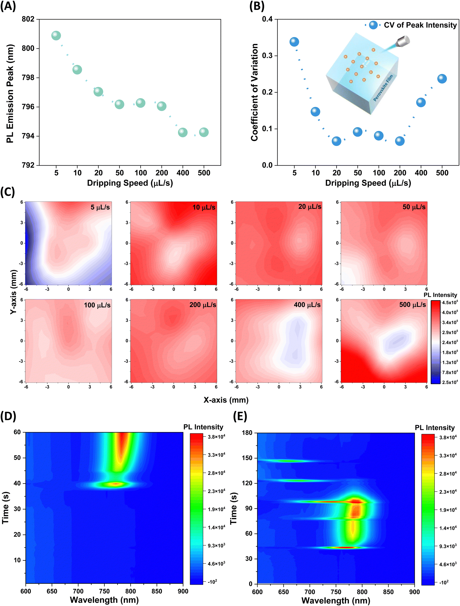 | ||
| Fig. 3 Optoelectronic properties of perovskite thin films. (A) PL emission peaks, (B) coefficient variation of PL peaks intensity, and (C) PL intensity contour map for perovskite films prepared with varying dripping speeds of ammonium halide precursor. The PL mapping figures are plotted as value maps of slices, with 13 specific points in each film collected. In situ PL spectra of wet perovskite films fabricated with (D) fast (>50 µL s−1) and (E) slow (∼0.5 µL s−1) dripping speeds of FAI/MACl solution. The PL signals were collected during the spin-coating process. | ||
Through careful optimization and regulation of each device preparation parameter, the overall performance of the devices is significantly enhanced compared to the initial samples. To further improve the device performance, a phenethylammonium iodide (PEAI) passivation layer was coated onto the perovskite surface (Fig. S21, ESI†).52Fig. 4A illustrates the J–V curves of the best device after optimization. The optimized perovskite devices demonstrate outstanding performance, boasting a PCE of 23.1%, a Jsc of 25.4 mA cm−2, an open-circuit voltage (Voc) of 1.15 V, and a FF of 0.79. These metrics significantly surpass those of the best manually fabricated control group devices (Fig. S22, ESI†). As indicated by the external quantum efficiency (EQE) spectrum (Fig. 4B), the integrated current density is consistent with the value obtained from the J–V curve with a slight deviation. The performance reproducibility was demonstrated through the repeated fabrication of devices with the optimized process parameters. The data in Fig. 4C demonstrate that these devices consistently achieve high performance with excellent reproducibility. The reproducibility and uniformity of device performance were further demonstrated by plotting the efficiency values histogram of 28 cells. The histogram shows that the efficiency values of most devices are concentrated within a relatively narrow range, without any noticeable outliers or irregular distributions. The performance of ambient-processed n–i–p devices prepared with/without additive engineering methods is summarized in Table S1 (ESI†). The data demonstrate that devices fabricated using the automated platform can achieve comparable or better performance. These results indicate that the optimized fabrication process is reliable and capable of producing devices with high consistency and uniformity.
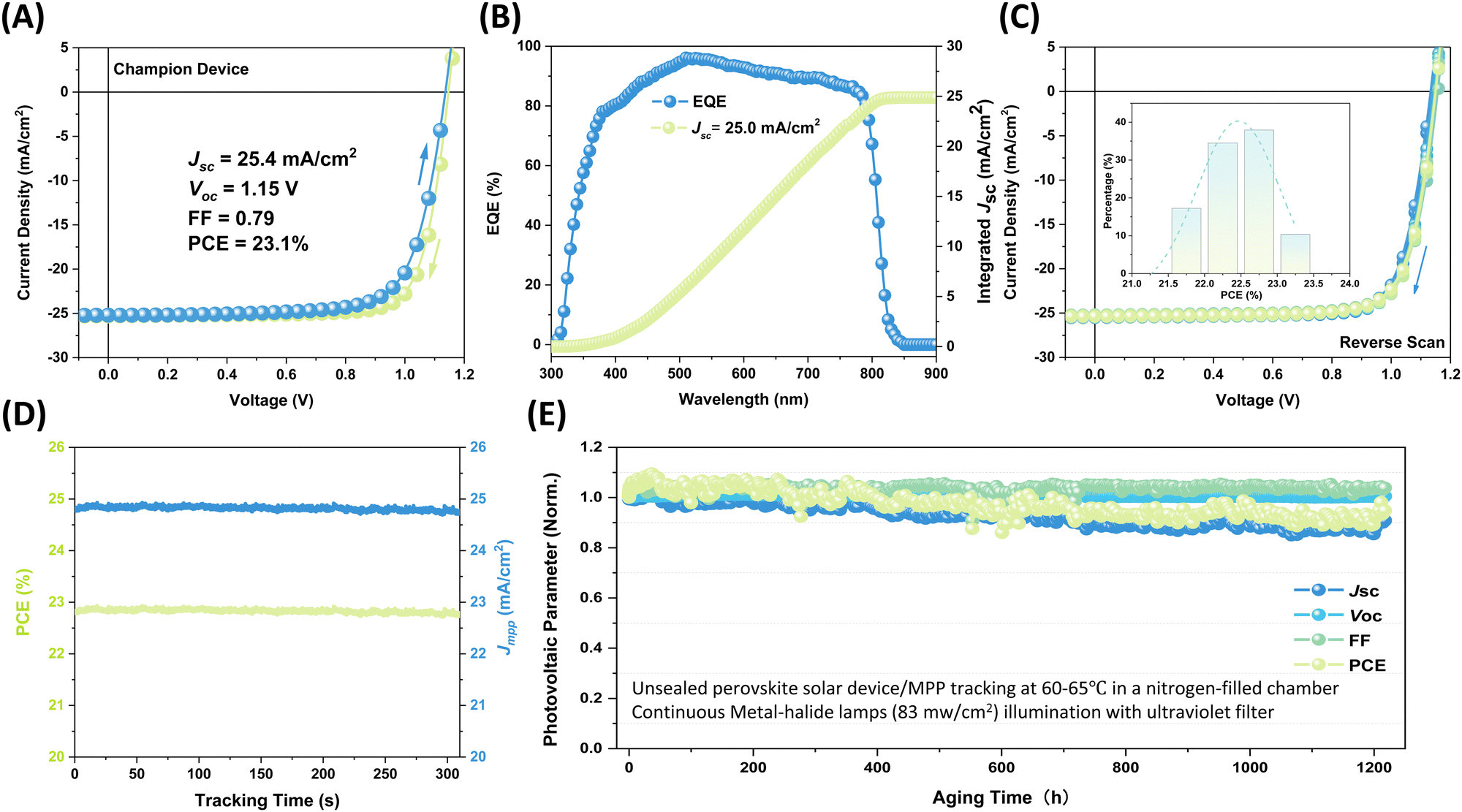 | ||
| Fig. 4 Characterizations of the optimized devices. (A) J–V curves of the champion device. Insert text provides the performance information. The spin speed combination is 1300 rpm × 1750 rpm, the dripping speed is 50 µL s−1. (B) EQE spectrum and integrated Jsc of the optimized devices. (C) J–V curves and PCE distributions histogram (28 cells) for the devices fabricated with optimized parameters. (D) The MPP tracking of the unpacked device under simulated AM 1.5G illumination for approximately 300 s in ambient air with continuous nitrogen flow. The data is collected at Jmpp with a constant voltage (Vmpp) of 0.908 V. (E) The results of the long-term stability test. The samples were tested at 60–65 °C in a nitrogen-filled chamber under continuous metal-halide lamp illumination (83 mW cm−2) in reverse directions. | ||
With the satisfactory consistency of device performance achieved, we further assessed the stability of the devices. The steady-state output of the optimized devices was evaluated at the maximum power point (MPP) under standard conditions of 1-sun illumination and room temperature for 5 minutes. Notably, the steady-state output of the device remains stable over the test period, as evidenced by the consistent short-circuit current and PCE values (Fig. 4D). Another strong criterion for evaluating the stability of thin films and devices is the long-term operational lifetime under light-soaking and elevated temperatures. The photo-thermal stability of perovskite films, fabricated with varying dripping speeds, was examined by tracking the UV-Vis absorption spectra over time (Fig. S23, ESI†). Remarkably, all unsealed samples show negligible degradation after 2030 hours of aging at 65 °C in an N2-filled chamber under 1-sun metal-halide lamps. The devices were aged using the standard ISOS-L-3 protocol, which involves maintaining the devices at 65 °C with the MPP tracking under continuous light exposure.53–55 Considering the photo-thermal instability of spiro-OMeTAD and PEA+ in FA+-containing perovskites,56 here, we replaced them with more stable PDCBT and BCF-doped PTAA bilayer configuration for photo-thermal stability testing.53,57 as shown in Fig. S24 (ESI†), the initial efficiency of the devices with the doped polymer bilayer was 21.2%, which is lower than the spiro-OMeTAD-based device. Given the thermal instability drawbacks of spiro-OMeTAD, future studies will be launched to discover thermally stable spiro-OMeTAD derivatives that can potentially match or exceed the efficiency. As shown in Fig. 4E and Fig. S25 (ESI†), the unsealed devices exhibit impressive stability behavior after continuous aging at 60–65 °C in a nitrogen-filled chamber under metal-halide lamps with an intensity of 83 mW cm−2. Specifically, the devices retained 93% ± 3% of their initial efficiency after 1200 hours. These findings not only validate the efficacy of enhancing device efficiency and durability through optimizing the fabrication process but also underscore the practical significance of optimized devices in real-world applications.
Summary and outlook
In this report, we utilized a fully automated device acceleration platform (DAP) named SPINBOT to systematically optimize the key parameters for the preparation of full perovskite devices in ambient air. Specifically, our study concentrated on analyzing the influence of the dripping speed of organic ammonium halide on perovskite films and devices. This involved a detailed examination of the relationship between processing conditions, structural characteristics, and device performance. Our findings indicate that moderate dropping speeds are critical for achieving high-performance devices. Conversely, excessively high or low speeds lead to performance degradation. Specifically, dripping speeds below 10 µL s−1 can result in the formation of non-perovskite phases, adversely affecting the overall device efficiency. These findings evidence why the manual preparation of high-performance devices still relies heavily on the empirical manipulation and decision-making of human experts in a single laboratory, and why “optimization procedures” often suffer from intra-laboratory reproducibility and laboratory-to-laboratory reproducibility. As a result, the optimized parameter set enabled us to achieve perovskite devices with efficiencies exceeding 23% and satisfactory stability under ambient conditions. This work not only emphasizes the critical role of precise control and optimization of process parameters in improving perovskite device performance but also the necessity to introduce DAP-like automated platforms to accelerate the development of high-performance perovskite photovoltaics. More importantly, this study highlights the potential of preparing high-performance perovskite devices in the air through precise control of process parameters, even with no use of additives in perovskite formulation, which is of great significance for the commercialization and practical application of perovskite solar photovoltaics.Looking to the future, we envision the establishment of an innovative and forward-thinking laboratory powered by Artificial Intelligence (AI), termed the Autonomous Material and Device Acceleration Platforms (AMADAP) laboratory, to further strengthen and universalize autonomous functional solar materials discovery and development as a prerequisite for developing digital twin models with inverse predictive power.58
Data availability
The data supporting this article have been included in this article or as part of the ESI.†Author contributions
J. Z. and C. J. B. conceptualized the research project. J. Z. designed and performed the whole sample fabrication experiments. J. Z. and J. W. tested the perovskite thin films. A. B. performed SEM measurement. S. Q., J. Z., and T. D. performed in situ PL characterization. J. Z. and J. W. analyzed the device data. J. Z., Y. Z., Z. P., and T. H. carried out the device stability test. V. L. guided the optimization process. F. S. smoothed the automated platform. J. A. H. and C. J. B. supervised the project. J. Z. made the figures and wrote the manuscript. C. J. B. contributed mainly to the framework revision of the manuscript. J. W., T. D., S. Q., K. Z., and C. L. contributed to the editing of the manuscript. All authors contributed to the discussion of experimental results and the manuscript.Conflicts of interest
The authors declare no competing interests.Acknowledgements
J. Z., J. A. H., and C. J. B. gratefully acknowledge the grants AutoPeroSol (ZT-I-PF-3-020) and AI-InSu-Pero (ZT-I-PF-5-106) by the Helmholtz Foundation. J. Z., K. Z., Z. P., J. T., CH. L., and C. L. gratefully acknowledge financial support from the China Scholarship Council (CSC). J. W. gratefully acknowledges financial support from the Sino-German Postdoc Scholarship Program (CSC-DAAD). C. L. gratefully acknowledges financial support from the Solar Tap (E1120206). J. A. H. and C. J. B. gratefully acknowledge the grants “ELF-PVDesign and development of solution processed functional materials for the next generations of PV technologies” (No. 44-6521a/20/4) by the Bavarian State Government. C. J. B. gratefully acknowledges financial support through the “Aufbruch Bayern” initiative of the state of Bavaria (EnCN and “Solar Factory of the Future”), the Bavarian Initiative “Solar Technologies go Hybrid” (SolTech), and the German Research Foundation (DFG) SFB 953-No. 182849149, and GRK2495 (ITRG2495).References
- J. Y. Kim, J.-W. Lee, H. S. Jung, H. Shin and N.-G. Park, Chem. Rev., 2020, 120, 7867–7918 CrossRef CAS PubMed.
- H. J. Snaith, Nat. Mater., 2018, 17, 372–376 CrossRef CAS PubMed.
- O. Almora, D. Baran, G. C. Bazan, C. Berger, C. I. Cabrera, K. R. Catchpole, S. Erten-Ela, F. Guo, J. Hauch and A. W. Ho-Baillie, Adv. Energy Mater., 2021, 11, 2002774 CrossRef CAS.
- T. Wang, W. Deng, J. Cao and F. Yan, Adv. Energy Mater., 2023, 13, 2201436 CrossRef CAS.
- F. Ma, Y. Zhao, Z. Qu and J. You, Acc. Mater. Res., 2023, 4, 716–725 CrossRef CAS.
- J. Jeong, M. Kim, J. Seo, H. Lu, P. Ahlawat, A. Mishra, Y. Yang, M. A. Hope, F. T. Eickemeyer and M. Kim, Nature, 2021, 592, 381–385 CrossRef CAS PubMed.
- H. Min, D. Y. Lee, J. Kim, G. Kim, K. S. Lee, J. Kim, M. J. Paik, Y. K. Kim, K. S. Kim, M. G. Kim, T. J. Shin and S. Il Seok, Nature, 2021, 598, 444–450 CrossRef CAS PubMed.
- G. Wang, Q. Lian, D. Wang, F. Jiang, G. Mi, D. Li, Y. Huang, Y. Wang, X. Yao, R. Shi, C. Liao, J. Zheng, A. Ho-Baillie, A. Amini, B. Xu and C. Cheng, Adv. Mater., 2022, 34, 2205143 CrossRef CAS PubMed.
- L. Yan, H. Huang, P. Cui, S. Du, Z. Lan, Y. Yang, S. Qu, X. Wang, Q. Zhang, B. Liu, X. Yue, X. Zhao, Y. Li, H. Li, J. Ji and M. Li, Nat. Energy, 2023, 8, 1158–1167 CrossRef CAS.
- Z. Liu, N. Rolston, A. C. Flick, T. W. Colburn, Z. Ren, R. H. Dauskardt and T. Buonassisi, Joule, 2022, 6, 834–849 CrossRef CAS.
- I. M. De Los Santos, H. J. Cortina-Marrero, M. Ruíz-Sánchez, L. Hechavarría-Difur, F. Sánchez-Rodríguez, M. Courel and H. Hu, Sol. Energy, 2020, 199, 198–205 CrossRef.
- M. Awais, D. Thrithamarassery Gangadharan, F. Tan and M. I. Saidaminov, Chem. Mater., 2022, 34, 8112–8118 CrossRef CAS.
- B. Cao, L. A. Adutwum, A. O. Oliynyk, E. J. Luber, B. C. Olsen, A. Mar and J. M. Buriak, ACS Nano, 2018, 12, 7434–7444 CrossRef CAS PubMed.
- J. George and G. Hautier, Trends Chem., 2021, 3, 86–95 CrossRef CAS.
- K. P. Goetz and Y. Vaynzof, ACS Energy Lett., 2022, 7, 1750–1757 CrossRef CAS.
- J. Wagner, C. G. Berger, X. Du, T. Stubhan, J. A. Hauch and C. J. Brabec, J. Mater. Sci., 2021, 56, 16422–16446 CrossRef CAS.
- N. J. Szymanski, B. Rendy, Y. Fei, R. E. Kumar, T. He, D. Milsted, M. J. McDermott, M. Gallant, E. D. Cubuk and A. Merchant, Nature, 2023, 1–6 CAS.
- X. Du, L. Lüer, T. Heumueller, J. Wagner, C. Berger, T. Osterrieder, J. Wortmann, S. Langner, U. Vongsaysy, M. Bertrand, N. Li, T. Stubhan, J. Hauch and C. J. Brabec, Joule, 2021, 5, 495–506 CrossRef CAS.
- D. P. Tabor, L. M. Roch, S. K. Saikin, C. Kreisbeck, D. Sheberla, J. H. Montoya, S. Dwaraknath, M. Aykol, C. Ortiz, H. Tribukait, C. Amador-Bedolla, C. J. Brabec, B. Maruyama, K. A. Persson and A. Aspuru-Guzik, Nat. Rev. Mater., 2018, 3, 5–20 CrossRef CAS.
- T. C. Wu, A. Aguilar-Granda, K. Hotta, S. A. Yazdani, R. Pollice, J. Vestfrid, H. Hao, C. Lavigne, M. Seifrid, N. Angello, F. Bencheikh, J. E. Hein, M. Burke, C. Adachi and A. Aspuru-Guzik, Adv. Mater., 2023, 35, 2207070 CrossRef CAS PubMed.
- J. Zhang, J. A. Hauch and C. J. Brabec, Acc. Chem. Res., 2024, 57, 1434–1445 CrossRef CAS PubMed.
- T. Osterrieder, F. Schmitt, L. Lüer, J. Wagner, T. Heumüller, J. Hauch and C. J. Brabec, Energy Environ. Sci., 2023, 16, 3984–3993 RSC.
- B. P. MacLeod, F. G. Parlane, T. D. Morrissey, F. Häse, L. M. Roch, K. E. Dettelbach, R. Moreira, L. P. Yunker, M. B. Rooney and J. R. Deeth, Sci. Adv., 2020, 6, eaaz8867 CrossRef CAS PubMed.
- M. Seifrid, R. Pollice, A. Aguilar-Granda, Z. Morgan Chan, K. Hotta, C. T. Ser, J. Vestfrid, T. C. Wu and A. Aspuru-Guzik, Acc. Chem. Res., 2022, 55, 2454–2466 CrossRef CAS PubMed.
- Y. Shi, P. L. Prieto, T. Zepel, S. Grunert and J. E. Hein, Acc. Chem. Res., 2021, 54, 546–555 CrossRef CAS PubMed.
- Q. Zhu, Y. Huang, D. Zhou, L. Zhao, L. Guo, R. Yang, Z. Sun, M. Luo, F. Zhang and H. Xiao, Nat. Synth., 2023, 1–10 Search PubMed.
- C. W. Coley, D. A. Thomas III, J. A. Lummiss, J. N. Jaworski, C. P. Breen, V. Schultz, T. Hart, J. S. Fishman, L. Rogers and H. Gao, Science, 2019, 365, eaax1566 CrossRef CAS PubMed.
- J. Wu, J. Zhang, M. Hu, P. Reiser, L. Torresi, P. Friederich, L. Lahn, O. Kasian, D. M. Guldi, M. E. Pérez-Ojeda, A. Barabash, J. S. Rocha-Ortiz, Y. Zhao, Z. Xie, J. Luo, Y. Wang, S. I. Seok, J. A. Hauch and C. J. Brabec, J. Am. Chem. Soc., 2023, 145, 16517–16525 CrossRef CAS PubMed.
- M. Liu, K. Chen, D. Christian, T. Fatima, N. Pissarnitski, E. Streckfuss, C. Zhang, L. Xia, S. Borges and Z. Shi, ACS Comb. Sci., 2012, 14, 51–59 CrossRef PubMed.
- Y. Huang, R. U. Sheth, S. Zhao, L. A. Cohen, K. Dabaghi, T. Moody, Y. Sun, D. Ricaurte, M. Richardson, F. Velez-Cortes, T. Blazejewski, A. Kaufman, C. Ronda and H. H. Wang, Nat. Biotechnol., 2023, 41, 1424–1433 CrossRef CAS PubMed.
- W. Zeng, L. Guo, S. Xu, J. Chen and J. Zhou, Trends Biotechnol., 2020, 38, 888–906 CrossRef CAS PubMed.
- Y. Zhao, J. Zhang, Z. Xu, S. Sun, S. Langner, N. T. P. Hartono, T. Heumueller, Y. Hou, J. Elia, N. Li, G. J. Matt, X. Du, W. Meng, A. Osvet, K. Zhang, T. Stubhan, Y. Feng, J. Hauch, E. H. Sargent, T. Buonassisi and C. J. Brabec, Nat. Commun., 2021, 12, 1–9 CrossRef PubMed.
- S. Sun, N. T. Hartono, Z. D. Ren, F. Oviedo, A. M. Buscemi, M. Layurova, D. X. Chen, T. Ogunfunmi, J. Thapa and S. Ramasamy, Joule, 2019, 3, 1437–1451 CrossRef CAS.
- S. Chen, Y. Hou, H. Chen, X. Tang, S. Langner, N. Li, T. Stubhan, I. Levchuk, E. Gu, A. Osvet and C. J. Brabec, Adv. Energy Mater., 2018, 8, 1701543 CrossRef.
- J. Zhang, J. Wu, S. Langner, B. Zhao, Z. Xie, J. A. Hauch, H. A. Afify, A. Barabash, J. Luo, M. Sytnyk, W. Meng, K. Zhang, C. Liu, A. Osvet, N. Li, M. Halik, W. Heiss, Y. Zhao and C. J. Brabec, Adv. Funct. Mater., 2022, 32, 2207101, DOI:10.1002/adfm.202207101.
- J. Yang, B. J. Lawrie, S. V. Kalinin and M. Ahmadi, Adv. Energy Mater., 2023, 2302337, DOI:10.1002/aenm.202302337.
- H. S. Stein and J. M. Gregoire, Chem. Sci., 2019, 10, 9640–9649 RSC.
- S. Li, H. Ren and Y. Yan, Appl. Surf. Sci., 2019, 484, 1191–1197 CrossRef CAS.
- J. Zhang, B. Liu, Z. Liu, J. Wu, S. Arnold, H. Shi, T. Osterrieder, J. A. Hauch, Z. Wu, J. Luo, J. Wagner, C. G. Berger, T. Stubhan, F. Schmitt, K. Zhang, M. Sytnyk, T. Heumueller, C. M. Sutter-Fella, I. M. Peters, Y. Zhao and C. J. Brabec, Adv. Energy Mater., 2023, 2302594, DOI:10.1002/aenm.202302594.
- H. Tan, A. Jain, O. Voznyy, X. Lan, F. P. García de Arquer, J. Z. Fan, R. Quintero-Bermudez, M. Yuan, B. Zhang and Y. Zhao, Science, 2017, 355, 722–726 CrossRef CAS PubMed.
- N. J. Jeon, J. H. Noh, Y. C. Kim, W. S. Yang, S. Ryu and S. I. Seok, Nat. Mater., 2014, 13, 897–903 CrossRef CAS PubMed.
- W. S. Yang, J. H. Noh, N. J. Jeon, Y. C. Kim, S. Ryu, J. Seo and S. I. Seok, Science, 2015, 348, 1234–1237 CrossRef CAS PubMed.
- Z. Ma, D. Huang, Q. Liu, G. Yan, Z. Xiao, D. Chen, J. Zhao, Y. Xiang, C. Peng and H. Li, J. Energy Chem., 2022, 66, 152–160 CrossRef CAS.
- L. Wang, C. McCleese, A. Kovalsky, Y. Zhao and C. Burda, J. Am. Chem. Soc., 2014, 136, 12205–12208 CrossRef CAS PubMed.
- Q. Chen, H. Zhou, T.-B. Song, S. Luo, Z. Hong, H.-S. Duan, L. Dou, Y. Liu and Y. Yang, Nano Lett., 2014, 14, 4158–4163 CrossRef CAS PubMed.
- Q. Jiang, Z. Chu, P. Wang, X. Yang, H. Liu, Y. Wang, Z. Yin, J. Wu, X. Zhang and J. You, Adv. Mater., 2017, 29, 1703852 CrossRef PubMed.
- H. Zhang, W. Yu, J. Guo, C. Xu, Z. Ren, K. Liu, G. Yang, M. Qin, J. Huang, Z. Chen, Q. Liang, D. Shen, Z. Wu, Y. Zhang, H. T. Chandran, J. Hao, Y. Zhu, C.-s Lee, X. Lu, Z. Zheng, J. Huang and G. Li, Adv. Energy Mater., 2022, 12, 2201663 CrossRef CAS.
- B.-w Park, N. Kedem, M. Kulbak, D. Y. Lee, W. S. Yang, N. J. Jeon, J. Seo, G. Kim, K. J. Kim, T. J. Shin, G. Hodes, D. Cahen and S. I. Seok, Nat. Commun., 2018, 9, 3301 CrossRef PubMed.
- J. Zhang, S. Langner, J. Wu, C. Kupfer, L. Lüer, W. Meng, B. Zhao, C. Liu, M. Daum, A. Osvet, N. Li, M. Halik, T. Stubhan, Y. Zhao, J. A. Hauch and C. J. Brabec, ACS Energy Lett., 2022, 7, 70–77 CrossRef CAS.
- S. Langner, F. Häse, J. D. Perea, T. Stubhan, J. Hauch, L. M. Roch, T. Heumueller, A. Aspuru-Guzik and C. J. Brabec, Adv. Mater., 2020, 32, 1907801 CrossRef CAS PubMed.
- J. Zhang, J. Wu, Y. Zhao, Y. Zou, A. Barabash, Z. Wu, K. Zhang, C. Deng, J. Elia, C. Li, J. S. Rocha-Ortiz, C. Liu, A. Saboor, I. M. Peters, J. A. Hauch and C. J. Brabec, ACS Energy Lett., 2023, 8, 3595–3603 CrossRef CAS.
- Q. Jiang, Y. Zhao, X. Zhang, X. Yang, Y. Chen, Z. Chu, Q. Ye, X. Li, Z. Yin and J. You, Nat. Photonics, 2019, 13, 460–466 CrossRef CAS.
- Y. Zhao, T. Heumueller, J. Zhang, J. Luo, O. Kasian, S. Langner, C. Kupfer, B. Liu, Y. Zhong, J. Elia, A. Osvet, J. Wu, C. Liu, Z. Wan, C. Jia, N. Li, J. Hauch and C. J. Brabec, Nat. Energy, 2022, 7, 144–152 CrossRef CAS.
- M. V. Khenkin, E. A. Katz, A. Abate, G. Bardizza, J. J. Berry, C. Brabec, F. Brunetti, V. Bulović, Q. Burlingame and A. Di Carlo, Nat. Energy, 2020, 5, 35–49 CrossRef.
- J. Luo, B. Liu, H. Yin, X. Zhou, M. Wu, H. Shi, J. Zhang, J. Elia, K. Zhang, J. Wu, Z. Xie, C. Liu, J. Yuan, Z. Wan, T. Heumueller, L. Lüer, E. Spiecker, N. Li, C. Jia, C. J. Brabec and Y. Zhao, Nat. Commun., 2024, 15, 2002 CrossRef CAS PubMed.
- M. Wang, Z. Shi, C. Fei, Z. J. D. Deng, G. Yang, S. P. Dunfield, D. P. Fenning and J. Huang, Nat. Energy, 2023, 8, 1229–1239 CrossRef CAS.
- Y. Hou, X. Du, S. Scheiner, D. P. McMeekin, Z. Wang, N. Li, M. S. Killian, H. Chen, M. Richter, I. Levchuk, N. Schrenker, E. Spiecker, T. Stubhan, N. A. Luechinger, A. Hirsch, P. Schmuki, H.-P. Steinrück, R. H. Fink, M. Halik, H. J. Snaith and C. J. Brabec, Science, 2017, 358, 1192–1197 CrossRef CAS PubMed.
- L. Lüer, I. M. Peters, V. M. L. Corre, K. Forberich, D. M. Guldi and C. J. Brabec, Adv. Mater., 2024, 36, 2308578 CrossRef PubMed.
Footnote |
| † Electronic supplementary information (ESI) available: Supplementary information includes the Experimental section, Fig. S1–S25, Table S1, and a Supplemental Video. See DOI: https://doi.org/10.1039/d4ee01432d |
| This journal is © The Royal Society of Chemistry 2024 |