
 Open Access Article
 This Open Access Article is licensed under a Creative Commons Attribution-Non Commercial 3.0 Unported Licence
Strong thickness dependence in thin film photocatalytic heterojunctions: the ZnO–Bi2O3 case study†
Alberto
Bernal-Díaz
,
Agileo
Hernández-Gordillo
 ,
Juan Carlos
Alonso
,
Sandra E.
Rodil
and
Monserrat
Bizarro
*
,
Juan Carlos
Alonso
,
Sandra E.
Rodil
and
Monserrat
Bizarro
*
Instituto de Investigaciones en Materiales, Universidad Nacional Autónoma de México, Circuito Exterior S/N, Cd. Universitaria, Coyoacán, Mexico City, 04510, Mexico. E-mail: monserrat@materiales.unam.mx
First published on 3rd April 2024
Abstract
Semiconductor heterojunctions are an effective way to achieve efficient photocatalysts, as they can provide an adequate redox potential with visible light excitation. Several works have reported synergistic effects with nanoparticle semiconductor materials. The question is still open for thin film heterojunctions formed by stacked layers, as photocatalysis is considered a surface phenomenon. To investigate if the internal layer really affects or modifies the photocatalytic properties of the external material, we analyze the thin film heterojunction with ZnO and Bi2O3 semiconductors deposited by spray pyrolysis in two configurations: substrate/ZnO/Bi2O3 and substrate/Bi2O3/ZnO. Microstructural analysis was performed to verify the formation of the physical junction of the materials and discard new ternary phases. The photocatalytic activity was analyzed as a function of the thickness of the layers under blue light irradiation. We determined the conduction and valence bands positions, the carrier concentrations, mobilities, Fermi levels, etc. that allowed us to distinguish two reaction mechanisms depending on the configuration. There is a strong compromise between the order and thickness of the layers with the photocatalytic activity. The internal electric field produced in the interface defines the route of the photogenerated charges, and therefore the photocatalytic response. Thus, well-designed thin film heterojunctions can indeed improve the photocatalytic activity of the surface layer.
1. Introduction
Photocatalysis technology has been extensively investigated due to its ability to achieve the decomposition and mineralization of organic pollutants in water that are difficult to remove with traditional methods. In the photocatalytic process, a semiconductor is irradiated with light of higher energy than its bandgap (Eg) to promote electrons from the valence band (VB) to the conduction band (CB), thus generating electron–hole pairs. If these pairs migrate to the surface of the photocatalyst material, they may be responsible for the subsequent redox reactions that can be applied to the degradation of pollutants. Currently, the development of photocatalysts presents different challenges that must be faced: (i) the utilization of visible light, that implies a narrow band gap semiconductor; (ii) avoidance of the rapid recombination of the photo-excited carriers; and (iii) a good redox potential ability. This last feature implies an adequate position of the VB that allows the direct pollutant oxidation by holes or by the generation of reactive oxygen species, such as the hydroxyl radical (˙OH). However, a narrow band gap also implies a shift of the CB position and therefore, the generation of superoxide ion radical (O2˙−) could be affected, perceiving oneself as a poor redox power.1–6An efficient strategy to solve this problem is forming heterojunctions by coupling two semiconductors with staggered bands;2,7–11 one semiconductor should have a more negative CB position and the other a more positive VB position. The key to taking advantage of this junction is to keep the high reduction potential of the most negative CB and the high oxidation potential of the most positive VB. This junction configuration was first named as S-scheme by Q. Xu and coworkers12 to avoid confusion with the several variants of the “Z-scheme”.13 They emphasized that the charge transfer route of this S-scheme is completely different from the typical type-II heterojunction (in which the active bands end up being those with the lowest redox potential).
Most of the reported heterojunctions are in form of powders of composite nanoparticles, including different materials such as binary or ternary metal oxides (Fe2TiO5, SrTiO3, BiVO4, etc.), sulfides (CdS, ZnS, In2S3, etc.) and even graphitic carbon nanoparticles (g-C3N4).14 Nevertheless, these nanoparticle systems require an extra procedure to recover them from water at the end of the photocatalytic treatment process. For this reason, thin film heterojunctions are an attractive option for study their application in water treatment. Although there are several works that report thin film heterojunctions of different combined materials, such as GaAs/AlGaAs, ZnMgO/ZnO, In2O3/ZnO, MoS2/MoSe2, GaN/Zn,15,16 most of them are devoted to microelectronics, optoelectronics, and photovoltaic devices applications.17–19 The use of thin film heterojunctions in photocatalysis is still limited, but recent works show that heterojunctions such as TiO2/CuO,20 Cu2O/ZnO,21 Ag/BiVO4,22etc., present a better photocatalytic performance than the individual materials. Two interesting materials to couple are ZnO and Bi2O3 as their coupling could take advantage of the good redox potential of ZnO as well as its ability to form different nanostructures,23 and the visible light absorption of Bi2O3 due to its band gap close to 2.5 eV.24 For instance, Medina et al., showed that 2D-heterojunction produced by Bi2O3 dots deposited by sputtering onto a ZnO thin films growth on glass substrates by spray pyrolysis showed an improvement of the photocatalytic activity for the degradation of organic dyes.25 Moreover, Arana-Trenado, et al., showed that in thin film heterojunctions of BiOI–BiOBr, the order of the layers plays a crucial role in the photocatalytic response, finding that in one case the response is boosted, while in the opposite configuration is quenched.26 However, none of these works focus on the influence of the thickness of each layer in the photocatalytic response of the heterojunctions. In fact, a typical position is to think that “since photocatalysis is a surface phenomenon, the outermost layer is the only one relevant for the process, and the internal layer is useless”.
In this work, ZnO and Bi2O3 thin film heterojunctions were prepared by spray pyrolysis to demonstrate that not only the order of the layers but also their thickness have a strong influence on the charge transport that affects the photocatalytic property of the composite material. We optimized the thicknesses for which an enhanced photocatalytic response is obtained when ZnO is either at the surface or as internal layer and explain the different mechanisms that govern the photocatalytic reactions.
2. Experimental methods
All the films were deposited by spray pyrolysis technique on Corning® glass substrates (2.5 × 1.25 cm2). All the reactants were purchased from Sigma-Aldrich and used as received. For ZnO films a 0.2 M solution of zinc acetate (Zn(CH3COO)2·2H2O) was prepared in deionized water. The deposition temperature was 470 °C with solution and air flow rates of 8 and 1028 mL min−1, respectively. For Bi2O3 films, bismuth(III) acetate (Bi(CH3CO2)3) was dissolved in 25% vol acetic acid at 45 °C and 75% vol of water was added dropwise to get a 0.05 M homogeneous solution. The deposition temperature was 365 °C and the solution and air flow rates were 4 and 1130 mL min−1, respectively. The deposition time was varied to get films with different thickness of the individual materials. The most suitable thicknesses were selected based on the photocatalytic activity response.The heterojunction films were formed by the consecutive deposition of each precursor solution using the respective conditions described previously, thus obtaining the configurations S/ZnO/Bi2O3 and S/Bi2O3/ZnO, where S stands for “substrate”. The thickness of each layer was optimized by varying the deposition time of the top layer, while the bottom layer was kept constant (using the optimum thickness found in the individual material) and then, the thickness of the bottom layer was varied, while the top layer was kept constant with the value obtained in the previous step. The same procedure was performed for both configurations. Fig. 1a shows the schematic sequence of the deposition procedure. To identify each sample, the name was assigned with “Z” or “B” for ZnO or Bi2O3, respectively, followed by the deposition time used (3, 6, 9, 12 or 15 min), for example Z12B6 or B6Z9.
 | ||
| Fig. 1 (a) Schematic procedure for the deposition of ZnO and Bi2O3 thin films individually and in heterojunction; (b) XRD pattern of individual and heterojunction samples; (c) transmittance of the individual samples with different thickness; (d) kinetic rate constant of the photocatalytic reaction of ZnO and Bi2O3 films with different thicknesses. | ||
The samples were analyzed by X-ray diffraction using a Rigaku Ultima IV (Cu-Kα λ = 0.15418 nm) in a 2θ angle deflection range from 20° to 70°. The thickness was measured with a profilometer Dektak IIA. The optical properties were evaluated with a Shimadzu 2600 UV-vis spectrophotometer equipped with an integration sphere and using BaSO4 as a blank reference. SEM images were acquired with a JEOL 7600F scanning electron microscope. The photocatalytic activity of the films was tested using 15 mL of an aqueous solution of indigo carmine (IC) organic dye in a concentration of 5 mgL−1, with a natural pH around 6. The deposited samples were immersed in the IC solution for 30 min in the dark under constant stirring (1200 rpm) to achieve the equilibrium. Then each vial with the film and solution was irradiated using a blue LED lamp Asahi Spectra (λ = 405 nm, irradiance 1.1 W cm−2 measured with an OPTIMUM spectral light SRI-2000UV). The absorbance spectrum of IC solution was recorded every 30 min with a Shimadzu 1800 UV-vis spectrophotometer. An indirect determination of hydroxyl radicals (˙OH) was performed with the fluorescence of 2-hydroxyterephtalic acid (HTA) at 425 nm. For this, a solution 0.5 mM of terephtalic acid (TA) was prepared using an aqueous solution 2 mM of NaOH. Each sample was immersed in 15 mL of TA solution and left under dark conditions and constant stirring (1200 rpm) during 30 min. Then the samples were illuminated using the same photocatalytic conditions. The fluorescence was measured with an FS5 Edinburgh Instruments spectrofluorometer using an excitation wavelength of 312 nm.
Hall measurements were performed with an Ecopia HMS-3000 system, to determine the electrical resistivity, carrier concentration and mobility using the four-point probe Van der Pauw method. Electrochemical measurements were performed with a Gamry reference 600 potentiostat using the Echem Gamry software in a three-electrode quartz cell. The working electrode was the semiconductor film deposited over an FTO-coated glass with an exposed area of 0.25 cm2. The reference electrode was Ag/AgCl = 0.210 V/SHE and the counter electrode was a Pt wire. The electrolyte used was an aqueous solution containing 0.03 M KClO4 and 5 mg L−1 IC dye. The flat band potential (Vfb) of the films was estimated from Mott–Schottky plots acquired at frequencies of 8–80 Hz for ZnO and 800–1200 for Bi2O3.
3. Results and discussion
Fig. 1b shows the XRD pattern of individual ZnO and Bi2O3 films as well as S/ZnO/Bi2O3 and S/Bi2O3/ZnO heterojunctions. Individual Bi2O3 pattern (red) shows a beta phase corresponding to tetragonal crystal system identified with the ICDD PDF 01-078-1793. The observed diffraction peaks are relative to the planes (201), (211), (002), (220) and (222). The strongest intensity is along the plane (201). Individual ZnO pattern (blue) shows a hexagonal wurtzite phase identified with PDF 01-075-9742 and shows the diffraction peaks relative to the planes (100), (002), (101) and (103). The strongest intensity is along the plane (002) indicating its typical preferred orientation along the c-axis.27–29 In the case of the heterojunction S/ZnO/Bi2O3, the strongest intensity is along the plane (201) of Bi2O3 and is possible to observe the presence of diffraction peaks corresponding to the (002), (100) and (101) planes of ZnO but with less intensity. On the other hand, in the case of S/Bi2O3/ZnO, the evident diffraction peaks are those of ZnO, but the peaks corresponding to Bi2O3 are difficult to distinguish due to their low intensity. This denotes that the dominant diffraction peaks correspond to the top layer of the heterojunction. It can also be observed that, beyond the screening of the peaks, Bi2O3 grows different on the glass substrate than over ZnO layer, as the relative intensities of the peaks change.Fig. 1c presents the transmittance of the individual ZnO and Bi2O3 films at different deposition times. The graphs show that the thicker the layer, the more difficult it is for light to pass through. Since in photocatalytic heterojunctions both materials must participate in the process, it is necessary that both can be excited with light (in the present work we used blue light at λ = 405 nm, emission spectrum shown in Fig. 1c). The photocatalytic activity of the individual ZnO and Bi2O3 films was evaluated in the IC degradation at natural pH under blue light as a function of the thickness (regulated by the deposition time). This wavelength was chosen to test the effectiveness of the heterojunctions under visible light. Although ZnO needs a photon wavelength of 385 nm to be excited (Eg = 3.22 eV, shown in Fig. S1a†), it shows activity due to its native defects.30–32 On the contrary, Bi2O3 just needs photon wavelengths shorter than 477 nm, as its Eg = 2.39 eV (see Fig. S1b†). Fig. 1d shows the apparent kinetic rate constant (kapp) of the individual films for the dye degradation as a function of the layer thickness. For ZnO it is appreciated that the kapp increases notably as the layer thickness increases (for deposition times up to 12 min, Z12), and then this rate decelerates tending to a plateau. This plateau behavior suggests that no more layers are activated due to the low light transmittance (Fig. 1c), then films thicker than ∼1600 nm will not contribute considerably more to the photocatalytic activity. For this reason, the thickest layers deposited during 15 min were discarded as top layers. Therefore, it is enough to use ZnO films of 1630 ± 15 nm (obtained at 12 min of deposition time). For Bi2O3 films, the kapp was considerably lower than for ZnO at the same conditions, but they show a similar increasing trend of kapp from B6 to B12 and then a plateau behavior at B15. B6 films of 690 ± 110 nm were selected based on their transmittance.
According to XRD results, the S/ZnO/Bi2O3 and S/Bi2O3/ZnO heterojunctions were successfully formed with the procedure depicted in Fig. 1a. Cross section FESEM images confirmed the presence and the close interaction of the two semiconductors, as can be observed in Fig. 2 for a representative heterojunction sample of each arrangement, labeled as B6Z6 and Z12B6. The elemental composition mapping also allows to distinguish the layers of Zn and Bi in both configurations. It is worth mentioning that the deposition rate of the two oxides on the glass substrate is very different. ZnO grows faster (∼135.54 nm min−1 at the first minutes) than Bi2O3 (∼90.49 nm min−1), giving films of very different thickness at the same deposition time (as illustrated in Fig. 1d). But when Bi2O3 grows over the ZnO layer, the deposition rate increases notably, whereas ZnO over Bi2O3 remains similar.
 | ||
| Fig. 2 Cross section FESEM images of representative heterojunction films (in the top) B6Z6 (S/Bi2O3/Zn) and Z12B6 (S/Bi2O3/ZnO) and the elemental mapping of Bi and Zn showing their distribution in the heterojunctions. | ||
The dye discoloration % of ZnO, Bi2O3 and their heterojunctions was plotted as a function of the deposition time (Fig. 3a) and was compared at 90 min of reaction (to avoid the diffusive regime). The plot shows that the photocatalytic activity of ZnO films increases rapidly until 9 min of deposition time and then the rate decreases reaching a limit value, as it was expected due to the considerable thickness achieved. The highest discoloration percentage was achieved by the thickest film (Z12, 1630 ± 15 nm). On the contrary, the film with the least activity was Bi2O3 (B3, 296 ± 76 nm), reaching only 6% dye discoloration at the same reaction conditions. Important changes are observed when both materials form the heterojunctions at different thickness layers. The first configuration to analyze is S/Bi2O3/ZnO, shown in Fig. 3a, with its two variants: (i) a Bi2O3 variable thickness bottom layer with ZnO fixed top layer (S/Bx/Z, open symbols and dashed line); and (ii) a Bi2O3 fixed bottom layer with ZnO variable thickness top layer (S/B/Zx, filled symbols and continuous line). For case (i), when the top ZnO layer is fixed at Z6 conditions (to warrantee a good light transmission through the film), it can be noticed that the Bi2O3 bottom layers B3 to B12 enhance the photocatalytic response of Z6, obtaining a maximum discoloration percentage of 57.4% for B6Z6 sample. This value is twice larger than the discoloration achieved by the individual Z6 film (27.6%). Thus, it is verified that the bottom layer has a positive contribution in the photocatalytic activity. Based on this result, the B6 film was selected as a fixed optimum thickness for the bottom layer of next case. Case (ii) shows a maximum photocatalytic discoloration of 80.8% with the heterojunction B6Z9. This value is higher than the obtained with the individual Z9 film (63.13%), and even higher than Z12 (70.25%). This indicates that the sample B6Z9 has the optimum thicknesses of both layers maximizing the synergistic effect. The hydroxyl radicals (˙OH) production was measured in samples Z9 and B6Z9 with the fluorescence of hydroxyterephtalic acid (HTA). As it can be observed in Fig. 3b, the heterojunction B6Z9 achieved 57% more intensity associated with an even better amount of ˙OH production than Z9 film. From this evidence we can affirm the following: first, the ˙OH radicals are only produced in the VB of ZnO layer; second, B6 bottom layer effectively contributes to accelerate or improve the photocatalytic process; and third, the B6Z9 heterojunction improves the charge separation and favors the ˙OH production of the outermost ZnO layer.
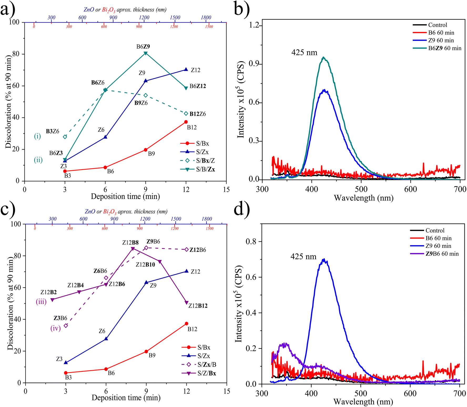 | ||
| Fig. 3 (a) Photocatalytic performance at 90 min of reaction of S/Bi2O3/ZnO heterojunctions: (i) with different thickness of the bottom layer and fixed top layer (S/Bx/Z, open symbols); (ii) with fixed bottom layer and different thickness of the top layer (S/B/Zx, closed symbols). (b) Comparison of the production of ˙OH radicals with samples B6, Z9 and B6Z9. (c) Photocatalytic performance at 90 min of reaction of S/ZnO/Bi2O3 heterojunctions: (iii) with fixed bottom layer and different thickness of the top layer (S/Z/Bx, closed symbols); (iv) with different thickness of the bottom layer and fixed top layer (S/Zx/B, open symbols). (d) Comparison of the production of ˙OH radicals with samples B6, Z9 and Z9B6. | ||
The second configuration to analyze is S/ZnO/Bi2O3, in which a priori the Bi2O3 top layer should be the active one. As we already know that Z12 film achieved the best photocatalytic response individually, we chose it as a fixed bottom layer. Then we varied the top Bi2O3 thickness (S/Z/Bx), as can be seen in plot marked as (iii) in Fig. 3c. Remarkably, all the heterojunction samples showed better dye discoloration % than the individual Bx. It is observed that a thin (∼300 nm) Bi2O3 film is greatly improved by the ZnO layer underneath, increasing the discoloration percentage from 6 to more than 50% (Z12B2, Z12B4, Z12B6). Nevertheless, if we compare these three heterojunctions with Z12 film, their performance is below. This indicates that the ZnO layer is being negatively affected by a reduction of the incident light arriving to its surface. However, when the thickness of the top Bi2O3 layer increases, the photocatalytic activity has a contribution of both layers, as seen in samples Z12B8 and Z12B10. If the thickness of the top layer increases even more, then the top Bi2O3 layer starts dominating the reaction and a decrease in the activity is noted (Z12B12).
The combined contribution of the two materials is clearly observed in case (iv) heterojunctions, when ZnO bottom thickness is variable (S/Zx/B) with fixed B6 conditions. Starting from Z3B6—the sample with the thinnest ZnO film underneath (425 ± 10 nm)—a synergistic effect is obtained, since both ZnO and Bi2O3 are notably improved respect their corresponding individual reference. This improvement shows an increasing trend as the thickness of the ZnO layer underneath grows, reaching a maximum value around 84% for Z9B6 and Z12B6. The samples Z9 and Z9B6 were further analyzed in the production of ˙OH radicals. As shown in Fig. 3d, the heterojunction Z9B6 exhibited negligible fluorescence indicative that fails to generate ˙OH radicals, while Z9 does. Considering that Bi2O3 is on the surface, the IC discoloration mechanism should occur by a different oxidation route than by ˙OH radicals previously observed for the opposite configuration B6Z9. Then, it is necessary to understand how Z9B6 and B6Z9 configurations improve the photocatalytic activity, either through of different charge separation mechanism or by generating different reactive oxygen species. For this, the absorbance spectra of IC dye were carefully analyzed, and further electrochemical measurements were also acquired.
The absorbance spectra of IC dye during the photocatalytic process show that the degradation mechanism is not the same for B6Z9 and Z9B6, as can be seen in Fig. 4. The IC's chromophore group, whose characteristic band appears at 610 nm, gradually decreases with the irradiation time. Simultaneously, an important change can be observed in the 200–300 nm range. The insets of Fig. 4 show this interval for the four samples (Z9, B6, B6Z9 and Z9B6) with the initial and final spectra. Both Z9 and B6Z9 (where ZnO layer is on the surface), present a progressively diminution of all the bands in the complete range (observed in Fig. 4a and c). It means that bands at 200–250 nm, characteristic of organic acids, are also decreased. This is an indicative of a degradation process of both IC molecule and its subproducts, which occur via oxidation with ˙OH radicals (as confirmed with the formation of hydroxyterephtalic acid, results shown in Fig. 3b). By contrast, when Bi2O3 is on the surface, the evolution of IC spectrum is different, as the bands in the UV range increase (Fig. 4b and d). Specifically in the heterojunction Z9B6, all the bands remain in the complete range, in addition, crossing points at 207 and 238 nm appear, which indicate the presence of the intermediate products, that have been identified as isatin sulfonic acid and 2-amino-5-sulfobenzoic acid.33 It is worth noting that this degradation process did not occur by hydroxyl radicals (˙OH), in agreement with the negligible hydroxyterephtalic acid production (as shown in Fig. 3d); then it has to be conducted by other species as the superoxide radicals (O2˙−) or the photogenerated holes, which achieve a discoloration process.34–37
 | ||
| Fig. 4 Photocatalytic evolution of IC absorbance spectrum with the samples (a) Z9, (b) B6, (c) B6Z9 and (d) Z9B6. | ||
To identify those responsible species a photocatalytic test was performed with sample Z9B6 using nitrogen bubbling to displace the dissolved oxygen and avoid the O2˙− generation. After 180 min of photocatalytic reaction, the IC relative concentration C/C0 remained close to unity, indicating that there was no degradation at all (Fig. 5a). As the absence of O2˙− stopped the reaction completely, it is possible to infer that h+ do not contribute to the reaction and the discoloration process observed in Fig. 4c is only due to formed O2˙− radicals in the presence of dissolved oxygen. This also means that the h+ photogenerated at the VB of Bi2O3 outermost layer should be possibly recombining with the e− generated at the CB of inner ZnO. At this point we can conclude that Z9B6 heterojunction's oxidating potential for the formation of (˙OH) radicals is modified, while that the reducing potential for the formation of O2˙− is maintained at the external Bi2O3 layer, and a clear contribution of the underneath layer is verified.
 | ||
| Fig. 5 (a) Photocatalysis test of Z9B6 with N2 bubbling as O2˙− scavenger and without scavengers; Mott–Schottky plots of (b) ZnO film and (c) Bi2O3 film; (d) EIS of the individual films and the heterojunction Z9B6 under illumination. | ||
Mott–Schottky analysis was performed at different frequencies (see Fig. 5b and c) to determine the CB positions of both n-type semiconductors, and the calculated values are presented in Table 1. It is observed that ZnO has an adequate VB position (3.1 V vs. NHE) to produce ˙OH radicals, whereas Bi2O3 has an adequate CB position (−0.70 V vs. NHE), for the formation of superoxide radicals.
| Parameter | ZnO | Bi2O3 |
|---|---|---|
| Semiconductor type | n | n |
| Band gap (Eg) | 3.22 [eV] | 2.39 [eV] |
| Conduction band (NHE) | −0.21 [V] | −0.70 [V] |
| Valence band (NHE) | 3.01 [V] | 1.69 [V] |
| Bulk concentration (Nd+) | −2.405 × 10¹³ [cm−3] | −1.083 × 10¹³ [cm−3] |
| Mobility | 1.896 × 101 [cm2 V−1 s−1] | 1.06 × 101 [cm2 V−1 s−1] |
| Hall coefficient | −2.548 × 10⁵ [cm3 C−1] | −3.178 × 10⁴ [cm3 C−1] |
Effective mass  |
0.24 | 1.2 |
| Fermi level (Ef) | −0.10 [V] | −0.31 [V] |
| Electrical permittivity | 8.5 [N m2 C−2]45–47 | 28 [N m2 C−2]48 |
| Effective density of states in the CB (Nc) | 2.948 × 10¹⁸ [cm−3] | 3.296 × 10¹⁹ [cm−3] |
| Thickness of the depletion region (xn) | 2.42 × 10⁻⁶ [m] | |
| Internal electric field (E0) | 16.92 × 10³ [V−1] | |
To evidence the impact of formed heterojunction on the charge transfer resistance, the electrochemical impedance spectroscopy (EIS) measurements were performed for Z9, B6 and Z9B6 samples under illumination conditions, recorded at the open-circuit potential to emulate the dye discoloration reaction conditions (Fig. 5d). It is observed that the measured impedances for B6 under illumination is considerably large (large Nyquist diagrams), suggesting high resistance registered without redox reaction. On the contrary, the Nyquist diagrams obtained for Z9 under illumination, showed the formation of a semicircle at low frequencies, indicating the occurrence of easy charge-transfer reactions, related to a low charge transfer resistance.38 In the recorded impedances for the Z9B6 heterojunction, the arc diameter is considerably lower when compared with the B6 material, suggesting a better separation of the photogenerated electrons and holes and a faster interfacial charge transfer, when Bi2O3 is deposited on top of ZnO layers. These results confirm that a synergistic effect was established through the semiconductor coupling.
In addition, Hall measurements were performed in the individual Z9 and B6 samples. These measurements allowed us to calculate parameters such as the Fermi level, the internal electric field (that implies a potential difference across the junction called “built-in potential”) and the potential shifts of the CBs when the two semiconductors are in contact forming the heterojunction,2,39–44 as follows:
 | (1) |
 | (2) |
 | (3) |
Giving a value of E0 = 16.92 × 10³ V m−1. With these values we sketched a band diagram showing the charge transfer in the heterojunctions. This helps to visualize the mechanisms involved in the photocatalytic reaction for both configurations, as presented in Fig. 6.
 | ||
| Fig. 6 Schematic representation of the band diagrams of individual semiconductors Bi2O3 and ZnO: (a) CB and VB positions before contact; (b) band bending and interfacial depletion region when the semiconductors are in contact showing the direction of E0; (c) illuminated S/Bi2O3/ZnO heterojunction and charge transfer during photocatalysis process; (d) illuminated S/ZnO/Bi2O3 heterojunction and charge transfer during photocatalysis process. | ||
With the measured parameters, we know that we formed a n–n heterojunction with staggered bands, where the CB of Bi2O3 is more negative than the CB of ZnO (Fig. 6a). We also observe that the VB potential of Bi2O3 does not allow the production of ˙OH radicals, (as demonstrated in Fig. 3), but ZnO does. Fig. 6b represents the charge redistribution at the interface of the semiconductors when they are in contact. Electrons diffuse from Bi2O3 to ZnO because the former has a higher Fermi level; the alignment of the Fermi levels produce the band bending and the depletion or accumulation regions in the interface of the heterojunction. At the same time, an internal electric field E0 pointing to the ZnO side is created. The calculated potential drop of the materials were: φBi2O3 = 0.0204 V and φZnO = 0.1495 V. Fig. 6c shows the photocatalysis process in the heterojunction with S/Bi2O3/ZnO configuration. In this case, the exposed surface is ZnO which receives a direct illumination with a 405 nm light. A small fraction of that light transmits through the film and arrives to the bottom Bi2O3 layer. In this configuration, due to the internal electric field E0 pointing to the ZnO side, the excited electrons in the CBZnO tend to migrate to the inner Bi2O3 layer. This internal E0 also helps the VBZnO holes to reach the outermost surface inducing the water oxidation and formation of ˙OH radicals, which are responsible of the IC dye degradation. The inner layer efficiently separates the photogenerated carriers, promoting a synergistic effect that improves the photocatalytic reaction with respect to the individual ZnO layer.
In the opposite configuration, S/ZnO/Bi2O3 shown in Fig. 6d, the E0 points inward and the photogenerated electrons in the CBBi2O3 are favored to migrate to the surface and interact with the dissolved oxygen to form superoxide (O2˙−) radicals. The transmitted light that arrives to the inner ZnO layer can slightly excite it, producing some electrons in the CBZnO; these electrons are driven by E0 to Bi2O3 layer and recombine with the photogenerated holes in VBBi2O3. Simultaneously, the holes created in the VBZnO are not favored to migrate to Bi2O3, but their accumulation can generate a charge concentration gradient favoring the diffusion phenomenon and modifying the surface properties of Bi2O3. The photocatalytic process in this configuration is then conducted by oxygen reduction reaction with the formation of O2˙− radicals, which are responsible of the IC dye discoloration.
After the careful analysis made for this specific case, we can affirm that thin film heterojunctions are different from powder heterojunctions, for this reason we avoid to label as “S-scheme” our heterojunction. The main differences in thin film heterojunctions are: (i) the illumination excites mainly the surface layer, and if it is thin enough, then some light can reach the inner layer and excite it too. (ii) The order of the layers matters as the built-in electric field will point from the semiconductor with high EF to the one with low EF. This in turn, will define the charge transport and the mechanism that will govern the photocatalytic reaction. (iii) There is only one active band at the surface that is responsible of the formation of the reactive species for the photocatalytic process.
4. Conclusions
There is indeed an influence in the photocatalytic activity of thin film heterojunctions due to the bottom semiconductor layer. A strong compromise between the thickness of both layers results in conditions where an enhanced photocatalytic activity is obtained. The internal electric field, created due to the difference in the band positions of the involved semiconductors, can drive the photogenerated carriers producing a completely different reaction mechanism depending on the order of the layers. In thin film heterojunctions it is important to consider that the illumination is not the same for both materials, and the active species are produced in only one active band, then is better not to label the process as “S-scheme”. In the case of Bi2O3/ZnO heterojunction, the internal electric field produced the following manifestations: (a) an effective charge separation in S/Bi2O3/ZnO that favored the ˙OH production; and (b) surface modification of S/ZnO/Bi2O3 allowing a better response than Bi2O3 by itself, due to the charge separation and the subsequent formation of O2˙− radicals. The degradation process by ˙OH radicals is notably faster and more effective than discoloration process by O2˙− radicals, as the subproducts are also oxidized contributing to a faster mineralization of the pollutant. A reasoned construction of thin film heterojunctions is necessary to achieve an enhanced photocatalytic activity.Author contributions
A. Bernal-Díaz: Investigation, methodology, data curation, formal analysis, writing-original draft. A. Hernández-Gordillo: Formal analysis, data curation, supervision, validation, writing-review & editing. J. C. Alonso: Resources, writing – review & editing. S. E. Rodil: Resources, writing – review & editing. M. Bizarro: Conceptualization, formal analysis, supervision, data curation, writing – original draft, writing – review & editing, project administration, funding acquisition.Conflicts of interest
The authors have no conflict of interest to declare.Acknowledgements
Authors fully acknowledge the technical support received from Lourdes Bazán, Adriana Tejeda, Carlos Ramos, Oralia Martínez, Teresa Vázquez, Yoarhy Amador. Authors are also grateful with Dr Guillermo Santana for the fruitful discussions. This project was funded by DGAPA-PAPIIT under Grant IN102521.References
- S. A. Younis and K. H. Kim, Heterogeneous Photocatalysis Scalability for Environmental Remediation: Opportunities and Challenges, Catalysts, 2020, 10(10), 1–8, DOI:10.3390/catal10101109.
- H. Yang, A Short Review on Heterojunction Photocatalysts: Carrier Transfer Behavior and Photocatalytic Mechanisms, Mater. Res. Bull., 2021, 142, 111406, DOI:10.1016/j.materresbull.2021.111406.
- J. Theerthagiri, S. Chandrasekaran, S. Salla, V. Elakkiya, R. A. Senthil, P. Nithyadharseni, T. Maiyalagan, K. Micheal, A. Ayeshamariam, M. V. Arasu, N. A. Al-Dhabi and H. S. Kim, Recent Developments of Metal Oxide Based Heterostructures for Photocatalytic Applications towards Environmental Remediation, J. Solid State Chem., 2018, 267, 35–52, DOI:10.1016/j.jssc.2018.08.006.
- Z. Wang, Z. Lin, S. Shen, W. Zhong and S. Cao, Advances in Designing Heterojunction Photocatalytic Materials, Chin. J. Catal., 2021, 42(5), 710–730, DOI:10.1016/S1872-2067(20)63698-1.
- Y. Wang, L. Shi, H. Hu, B. Qian, W. Hou, H. Li, X. Liu, D. Liu, S. Wu, H. Huang, X. Song, Y. Zhang and T. Ma, Binary Trinuclear Metal–oxo Sub–nanomaterials for Photocatalytic Hydrogen and Chlorine Production from Seawater, SusMat, 2022, 2(6), 708–719, DOI:10.1002/sus2.89.
- P. Song, J. Du, X. Ma, Y. Shi, X. Fang, D. Liu, S. Wei, Z. Liu, Y. Cao, B. Lin, J. Di, Y. Wang, J. Cui, T. Kong, C. Gao and Y. Xiong, Design of Bi 4 O 5 Br 2 /G–C 3 N 4 Heterojunction for Efficient Photocatalytic Removal of Persistent Organic Pollutants from Water, EcoEnergy, 2023, 1(1), 197–206, DOI:10.1002/ece2.8.
- A. S. Kshirsagar and P. K. Khanna, CuSbSe 2/TiO 2: Novel Type-II Heterojunction Nano-Photocatalyst, Mater. Chem. Front., 2019, 3(3), 437–449, 10.1039/c8qm00537k.
- V. K. Landge, S. H. Sonawane, M. Sivakumar, S. S. Sonawane, G. Uday Bhaskar Babu and G. Boczkaj, S-Scheme, Heterojunction Bi2O3-ZnO/Bentonite Clay Composite with Enhanced Photocatalytic Performance, Sustain. Energy Technol. Assess., 2021, 45, 101194, DOI:10.1016/j.seta.2021.101194.
- L. Xie, T. Du, J. Wang, Y. Ma, Y. Ni, Z. Liu, L. Zhang, C. Yang and J. Wang, Recent Advances on Heterojunction-Based Photocatalysts for the Degradation of Persistent Organic Pollutants, Chem. Eng. J., 2021, 426, 130617, DOI:10.1016/j.cej.2021.130617.
- J. Ren, W. Wang, L. Zhang, J. Chang and S. Hu, Photocatalytic Inactivation of Bacteria by Photocatalyst Bi2WO6under Visible Light, Catal. Commun., 2009, 10(14), 1940–1943, DOI:10.1016/j.catcom.2009.07.006.
- J. Ning, B. Zhang, L. Siqin, G. Liu, Q. Wu, S. Xue, T. Shao, F. Zhang, W. Zhang and X. Liu, Designing Advanced S-Scheme CdS QDs/La-Bi2WO6 Photocatalysts for Efficient Degradation of RhB, Exploration, 2023, 3(5), 20230050, DOI:10.1002/EXP.20230050.
- Q. Xu, L. Zhang, B. Cheng, J. Fan and J. Yu, S-Scheme, Heterojunction Photocatalyst, Chem, 2020, 6(7), 1543–1559, DOI:10.1016/j.chempr.2020.06.010.
- L. Jiang, H. Du, L. Li, X. Guan, Y. Zhang, L. Li, X. Liu, L. Li, Y. Tian, L. Zhang, S. Wang, J. Chen and S. Shen, Sequential Growth of Cs3Bi2I9/BiVO4 Direct Z-Scheme Heterojunction for Visible-Light-Driven Photocatalytic CO2 Reduction, Trans. Tianjin Univ., 2023, 29(6), 462–472, DOI:10.1007/s12209-023-00376-9.
- A. Balapure, J. Ray Dutta and R. Ganesan, Recent Advances in Semiconductor Heterojunctions: A Detailed Review of the Fundamentals of Photocatalysis, Charge Transfer Mechanism and Materials, RSC Appl. Interfaces, 2024, 1, 43–69, 10.1039/D3LF00126A.
- Z. Zheng, X. Zu, Y. Zhang and W. Zhou, Rational Design of Type-II Nano-Heterojunctions for Nanoscale Optoelectronics, Mater. Today Phys., 2020, 15, 100262, DOI:10.1016/j.mtphys.2020.100262.
- J. Lee and D. S. Chung, Heterojunction Oxide Thin Film Transistors: A Review of Recent Advances, J. Mater. Chem. C, 2023, 11, 5241–5256, 10.1039/d3tc00584d.
- M. Sharma, J. Panigrahi and V. K. Komarala, Nanocrystalline Silicon Thin Film Growth and Application for Silicon Heterojunction Solar Cells: A Short Review, Nanoscale Adv., 2021, 3(12), 3373–3383, 10.1039/d0na00791a.
- Q. Wang, L. Zhang, X. Liu and S. Li, Two-Dimensional Semiconductor Heterojunctions for Optoelectronics and Electronics, Front. Energy Res., 2021, 9, 802055, DOI:10.3389/fenrg.2021.802055.
- M. Purica, E. Budianu and E. Rusu, Heterojunction with ZnO Polycrystalline Thin Films for Optoelectronic Devices Applications; 2000, https://www.elsevier.nl/locate/mee Search PubMed.
- B. Hao, J. Guo, L. Zhang and H. Ma, Magnetron Sputtered TiO2/CuO Heterojunction Thin Films for Efficient Photocatalysis of Rhodamine B, J. Alloys Compd., 2022, 903, 163851, DOI:10.1016/j.jallcom.2022.163851.
- X. Yu, H. Chen, Q. Ji, Y. Chen, Y. Wei, N. Zhao and B. Yao, P-Cu, 2O/n-ZnO Heterojunction Thin Films with Enhanced Photoelectrochemical Properties and Photocatalytic Activities for Norfloxacin, Chemosphere, 2021, 267, 129285, DOI:10.1016/j.chemosphere.2020.129285.
- S. Bakhtiarnia, S. Sheibani, E. Aubry, H. Sun, P. Briois and M. Arab Pour Yazdi, One-Step Preparation of Ag-Incorporated BiVO4 Thin Films: Plasmon-Heterostructure Effect in Photocatalytic Activity Enhancement, Appl. Surf. Sci., 2022, 580, 152253, DOI:10.1016/j.apsusc.2021.152253.
- Z. L. Wang, Nanostructures of Zinc Oxide, Mater. Today, 2004, 7(6), 26–36 CrossRef CAS.
- K. Barrera-Mota, M. Bizarro, M. Castellino, A. Tagliaferro, A. Hernández and S. E. Rodil, Spray Deposited β-Bi2O3 Nanostructured Films with Visible Photocatalytic Activity for Solar Water Treatment, Photochem. Photobiol. Sci., 2015, 14(6), 1110–1119, 10.1039/c4pp00367e.
- J. C. Medina, N. S. Portillo-Vélez, M. Bizarro, A. Hernández-Gordillo and S. E. Rodil, Synergistic Effect of Supported ZnO/Bi2O3 Heterojunctions for Photocatalysis under Visible Light, Dyes Pigm., 2018, 153, 106–116, DOI:10.1016/j.dyepig.2018.02.006.
- J. A. Arana-Trenado, D. Ramírez-Ortega, A. Serrano-Lázaro, A. Hernández-Gordillo, S. E. Rodil and M. Bizarro, Synergistic Photocatalytic Effect of BiOBr-BiOI Heterojunctions Due to Appropriate Layer Stacking, Dalton Trans., 2022, 51(6), 2413–2427, 10.1039/d1dt03782j.
- M. Bizarro, High Photocatalytic Activity of ZnO and ZnO:Al Nanostructured Films Deposited by Spray Pyrolysis, Appl. Catal., B, 2010, 97(1–2), 198–203, DOI:10.1016/j.apcatb.2010.03.040.
- R. Ebrahimifard, H. Abdizadeh and M. R. Golobostanfard, Controlling the Extremely Preferred Orientation Texturing of Sol–Gel Derived ZnO Thin Films with Sol and Heat Treatment Parameters, J. Sol-Gel Sci. Technol., 2020, 93(1), 28–35, DOI:10.1007/s10971-019-05157-2.
- V. K. Jayaraman, A. Hernández-Gordillo and M. Bizarro, Importance of Precursor Type in Fabricating ZnO Thin Films for Photocatalytic Applications, Mater. Sci. Semicond. Process., 2018, 75, 36–42, DOI:10.1016/j.mssp.2017.11.015.
- A. Serrano-Lázaro, F. A. Verdín-Betancourt, V. K. Jayaraman, A. Hernández-Gordillo, M. d. L. López-González, A. Sierra-Santoyo, G. Santana and M. Bizarro, Tracing the Degradation Pathway of Temephos Pesticide Achieved with Photocatalytic ZnO Nanostructured Films, Environ. Sci.: Nano, 2022, 9(9), 3538–3550, 10.1039/d2en00384h.
- Z. Pei, L. Ding, J. Hu, S. Weng, Z. Zheng, M. Huang and P. Liu, Defect and Its Dominance in ZnO Films: A New Insight into the Role of Defect over Photocatalytic Activity, Appl. Catal., B, 2013, 142–143, 736–743, DOI:10.1016/j.apcatb.2013.05.055.
- D. Chen, Z. Wang, T. Ren, H. Ding, W. Yao, R. Zong and Y. Zhu, Influence of Defects on the Photocatalytic Activity of ZnO, J. Phys. Chem. C, 2014, 118(28), 15300–15307, DOI:10.1021/jp5033349.
- A. Hernández-Gordillo, V. Rodríguez-González, S. Oros-Ruiz and R. Gómez, Photodegradation of Indigo Carmine Dye by CdS Nanostructures under Blue-Light Irradiation Emitted by LEDs, Catal. Today, 2016, 266, 27–35, DOI:10.1016/j.cattod.2015.09.001.
- J. h. Li, J. Ren, Y. j. Hao, E. p. Zhou, Y. Wang, X. j. Wang, R. Su, Y. Liu, X. h. Qi and F. t. Li, Construction of β-Bi2O3/Bi2O2CO3 Heterojunction Photocatalyst for Deep Understanding the Importance of Separation Efficiency and Valence Band Position, J. Hazard. Mater., 2021, 401, 123262, DOI:10.1016/j.jhazmat.2020.123262.
- J. h. Qiao, K. Chen, S. j. Li, Y. c. Liu, H. w. Cao, G. Wei, L. p. Kong, X. Zhang and H. t. Liu, Plasma Spray–Chemical Vapor Deposition of Nanotextured Film with α/β Bi2O3 Heterostructure and Photocatalytic Degradation Performance, Vacuum, 2021, 188, 110206, DOI:10.1016/j.vacuum.2021.110206.
- B. Wang, H. Z. Qian and Y. Peng, 2D/1D Bi12O17Cl2/β-Bi2O3heterojunction Photocatalysts with Boosted Photocatalytic Performance, CrystEngComm, 2021, 23(30), 5190–5199, 10.1039/d1ce00472g.
- X. Yu, X. Huang, Y. Huang, Q. Feng, W. Chen, C. Ju, Y. Du, T. Bai and D. Wang, Crystal Phase Transition of β-Bi2O3 and Its Enhanced Photocatalytic Activities for Tetracycline Hydrochloride, Colloids Surf., A, 2021, 626, 127068, DOI:10.1016/j.colsurfa.2021.127068.
- D. Guerrero-Araque, D. Ramírez-Ortega, P. Acevedo-Peña, F. Tzompantzi, H. A. Calderón and R. Gómez, Interfacial Charge-Transfer Process across ZrO2-TiO2 Heterojunction and Its Impact on Photocatalytic Activity, J. Photochem. Photobiol., A, 2017, 335, 276–286, DOI:10.1016/j.jphotochem.2016.11.030.
- R. F. Pierret, in Semiconductor Device Fundamentals, ed. K. Harutunian, Addison Wesley, West Lafayette, 2nd edn, 1996 Search PubMed.
- R. F. Pierret and G. W. Neudeck, Modular Series on Solid State Devices. Advanced Semiconductor Fundamentals, Pearson Education, New Jersey, 2nd edn, 2002, vol. VI Search PubMed.
- L. Chen, J. T. Ren and Z. Y. Yuan, Enabling Internal Electric Fields to Enhance Energy and Environmental Catalysis, Adv. Energy Mater., 2023, 13(11), 2203720, DOI:10.1002/aenm.202203720.
- Z. Lou, P. Wang, B. Huang, Y. Dai, X. Qin, X. Zhang, Z. Wang and Y. Liu, Enhancing Charge Separation in Photocatalysts with Internal Polar Electric Fields, ChemPhotoChem, 2017, 1(5), 136–147, DOI:10.1002/cptc.201600057.
- X. Yue, J. Fan and Q. Xiang, Internal Electric Field on Steering Charge Migration: Modulations, Determinations and Energy-Related Applications. Advanced Functional Materials, John Wiley and Sons Inc, 2022. DOI:10.1002/adfm.202110258.
- L. Li, P. A. Salvador and G. S. Rohrer, Photocatalysts with Internal Electric Fields, Nanoscale, 2014, 6(1), 24–42, 10.1039/c3nr03998f.
- D. Kaur, A. Bharti, T. Sharma and C. Madhu, Dielectric Properties of ZnO-Based Nanocomposites and Their Potential Applications, Int. J. Opt., 2021, 2021, 9950202, DOI:10.1155/2021/9950202.
- J. Gulomov, O. Accouche, R. Aliev, R. Ghandour and I. Gulomova, Investigation of N-ZnO/p-Si and n-TiO2/p-Si Heterojunction Solar Cells: TCAD + DFT, IEEE Access, 2023, 11, 38970–38981, DOI:10.1109/ACCESS.2023.3268033.
- S. V. Vegesna, V. J. Bhat, D. Bürger, J. Dellith, I. Skorupa, O. G. Schmidt and H. Schmidt, Increased Static Dielectric Constant in ZnMnO and ZnCoO Thin Films with Bound Magnetic Polarons, Sci. Rep., 2020, 10(1), 6698, DOI:10.1038/s41598-020-63195-1.
- S. Patil and V. Puri, Electromagnetic Properties of Bismuth Oxide Thin Film Deposited on Glass and Alumina, Arch. Appl. Sci. Res., 2011, 3, 14–24 CAS.
Footnote |
| † Electronic supplementary information (ESI) available. See DOI: https://doi.org/10.1039/d4dt00697f |
| This journal is © The Royal Society of Chemistry 2024 |