
 Open Access Article
 This Open Access Article is licensed under a Creative Commons Attribution-Non Commercial 3.0 Unported Licence
Extrinsically conducting MOFs: guest-promoted enhancement of electrical conductivity, thin film fabrication and applications
Rajat
Saha
 * and
Carlos J.
Gómez García
*
* and
Carlos J.
Gómez García
*
Departamento de Química Inorgánica, Universidad de Valencia, Dr Moliner 50, 46100 Burjasot (Valencia), Spain. E-mail: Rajat.Saha@uv.es; carlos.gomez@uv.es
First published on 22nd August 2024
Abstract
Conductive metal–organic frameworks are of current interest in chemical science because of their applications in chemiresistive sensing, electrochemical energy storage, electrocatalysis, etc. Different strategies have been employed to design conductive frameworks. In this review, we discuss the influence of different types of guest species incorporated within the pores or channels of metal–organic frameworks (MOFs) and porous coordination polymers (PCPs) to generate charge transfer pathways and modulate their electrical conductivity. We have classified dopants or guest species into three different categories: (i) metal-based dopants, (ii) molecule and molecular entities and (iii) organic conducting polymers. Different types of metal ions, metal nano-clusters and metal oxides have been used to enhance electrical conductivity in MOFs. Metal ions and metal nano-clusters depend on the hopping process for efficient charge transfer whereas metal-oxides show charge transport through the metal–oxygen pathway. Several types of molecules or molecular entities ranging from neutral TCNQ, I2, and fullerene to ionic methyl viologen, organometallic like nickelcarborane, etc. have been used. In these cases, the charge transfer process varies with the guest species. When organic conducting polymers are the guest, the charge transport occurs through the polymer chains, mostly based on extended π-conjugation. Here we provide a comprehensive and critical review of these strategies to add electrical conductivity to the, in most cases, otherwise insulating MOFs and PCPs. We point out the guest encapsulation process, the geometry and structure of the resulting host–guest complex, the host–guest interactions and the charge transport mechanism for each case. We also present the methods for thin film fabrication of conducting MOFs (both, liquid–phase and gas–phase based methods) and their most relevant applications like electrocatalysis, sensing, charge storage, photoconductivity, photocatalysis,… We end this review with the main obstacles and challenges to be faced and the appealing perspectives of these 21st century materials.
 Rajat Saha | Rajat Saha received his PhD from Jadavpur University, India, in 2013 on designing multifunctional MOFs and organic materials using crystal engineering techniques. He joined as an Assistant Professor at the Department of Chemistry, Kazi Nazrul University, Asansol, India, in 2016. His research interests have mainly centered on designing MOFs for versatile applications. Presently, he is working as a Maria Zambrano Postdoctoral Fellow at Universitat de Valencia, Spain. Now, he is working on conducting MOFs for their applications in spintronics and others. |
 Carlos J. Gómez García | Carlos J. Gómez García (Valladolid, Spain, 1964) received his PhD from the University of Valencia with the extraordinary doctoral award in 1991. After performing two post-doctoral stays at Rennes and Bordeaux (France), he joined the University of Valencia as an associate professor in 1993. In 1998 he was promoted as assistant professor and as full professor in 2007 at the Inorganic Chemistry department at the University of Valencia (after a national habilitation). Since 2014 he leads the Multifunctional Modulable Molecular Materials (M4) group. His main interests are magnetic and conducting MOFs and coordination compounds, including polyoxometalate-based materials for energy applications. |
1. Introduction
Since 1999, after the discovery of MOF-5 by Yaghi et al., metal–organic frameworks (MOFs) or porous coordination polymers (PCPs) have become the most studied functional materials in chemical science.1–3 MOFs or PCPs, constructed using discrete metal ions or metal clusters as nodes and organic multi-topic ligands as spacers, have attracted significant attention not only due to their aesthetically beautiful architectures but also thanks to their large surface areas, chemically functionalized cavities, flexible skeletons and intriguing electronic properties.4–6 Such structural characteristics make them potential functional materials for gas and solvent adsorption,7 storage,8 separation,9 catalysis,10 sensing,11 drug delivery,12etc. Additionally, the almost infinite choice of organic bridging ligands and metal ions, with different oxidation states and coordination numbers, allows the modulation of their structures and properties in a controlled manner.13–15In order to obtain advanced functionalities, different crystal engineering design principles, including both pre- and post-synthetic modifications of the basic building blocks, have been employed to convert simple MOF structures into more complex ones.16–18 Such structural complexity can be achieved by the exchange of ligands or metal ions via post-synthetic methods19,20 or by grafting extra functional units either on the metal atom21 or on the ligand backbone.22 Multifunctional MOFs have also been designed by using different types of ligands and guests in simple MOFs.23 In this regard, the most promising design principle is the utilization of the inherent void space of MOFs to encapsulate different types of guest species that may modulate and create new functionalities different from those of the host MOF and the guest.24–27
In the last decade, electrically conductive MOFs and PCPs have gained much attention for their numerous applications in energy storage,28,29 electrocatalysis,30,31 chemiresistive sensing,32,33etc. However, the implication of MOFs in electronic and electrochemical applications is hindered by their low-charge transport properties. The poor overlap between metal d-orbitals and ligand donor p-orbitals results in weakly conducting or insulating materials.34 Given the enormous opportunity offered by conducting MOFs, several strategies have been used to increase and modulate their electrical conductivity: (a) the use of ligands having soft donor atoms like S, P, Se, etc., (b) the use of extended conjugated organic ligands, (c) the use of redox-active building blocks (metal ions and organic ligands), and (d) the incorporation of guest species within the pores/voids of the frameworks, etc.35–43 Based on the electron conduction pathway, electrically conductive MOFs are categorized into two classes: (i) intrinsically conducting MOFs (ic-MOFs), in which electron conduction proceeds only through the metal–ligand backbone, and (ii) extrinsically conducting MOFs (ec-MOFs), where electron conduction is dependent on the guest species present in the host framework.
In order to control the electrical conductivity of ic-MOFs, researchers have shown that the utilization of soft donor-based organic ligands is a very promising strategy to enhance their conductivity thanks to a better metal–ligand overlap.44,45 A nice example is MOF [Cu3(C6S6)]n, which contains an infinite [–Cu–S–] network and shows the highest reported conductivity for any MOFs.46 Different research groups have utilized extended conjugated organic ligands like pyrene, coronene, etc. to develop in-plane charge transport. An example of this strategy is MOF PTC-Fe (PTC = 1,2,3,4,5,6,7,8,9,10,11,12-perthiolated coronene), which has a coronene core with S donor atoms and shows a high electrical conductivity.47 The presence of mixed-valence metal ions can also improve the electrical conductivity. Thus, Long et al. have reported a billion-fold increase in the electrical conductivity of MOFs by using mixed-valence metal ions.48 On the other hand, the Harris group has shown that the use of radical-based ligands can increase the overall charge transport properties of MOFs and PCPs.49 Furthermore, defect healing can improve the intrinsic charge transport properties of MOFs.50 The detailed structural analysis has allowed a significant improvement and development of ic-MOFs and PCPs in the last decade.
Unfortunately, the incorporation of guests within the channels or cavities of these ic-MOFs and PCPs to prepare ec-MOFs induces a loss of crystallinity of the MOFs in most cases,51 rendering the study and development of ec-MOFs, in a rational way, very difficult. Nevertheless, there has been substantial growth in this field in the last few years.
Although a few review articles have focused on the guest-dependent electrical conductivity of MOFs, the major focus has been placed on intrinsically conducting frameworks.28,31,34–36,52–59 From the structural point of view, the design of ic-MOFs has gained much attention, and, therefore, most of the reviews are centred on the structure–property relationship of these ic-MOFs, while for the guest-dependent conducting ec-MOFs, the focus has been mostly centred on TCNQ,60 iodine,61 polyiodides62 and some conducting polymers.63 However, to date, there have been no comprehensive reviews highlighting all the factors associated with the guest-dependent electrical conductivity of these ec-MOFs (Fig. 1).
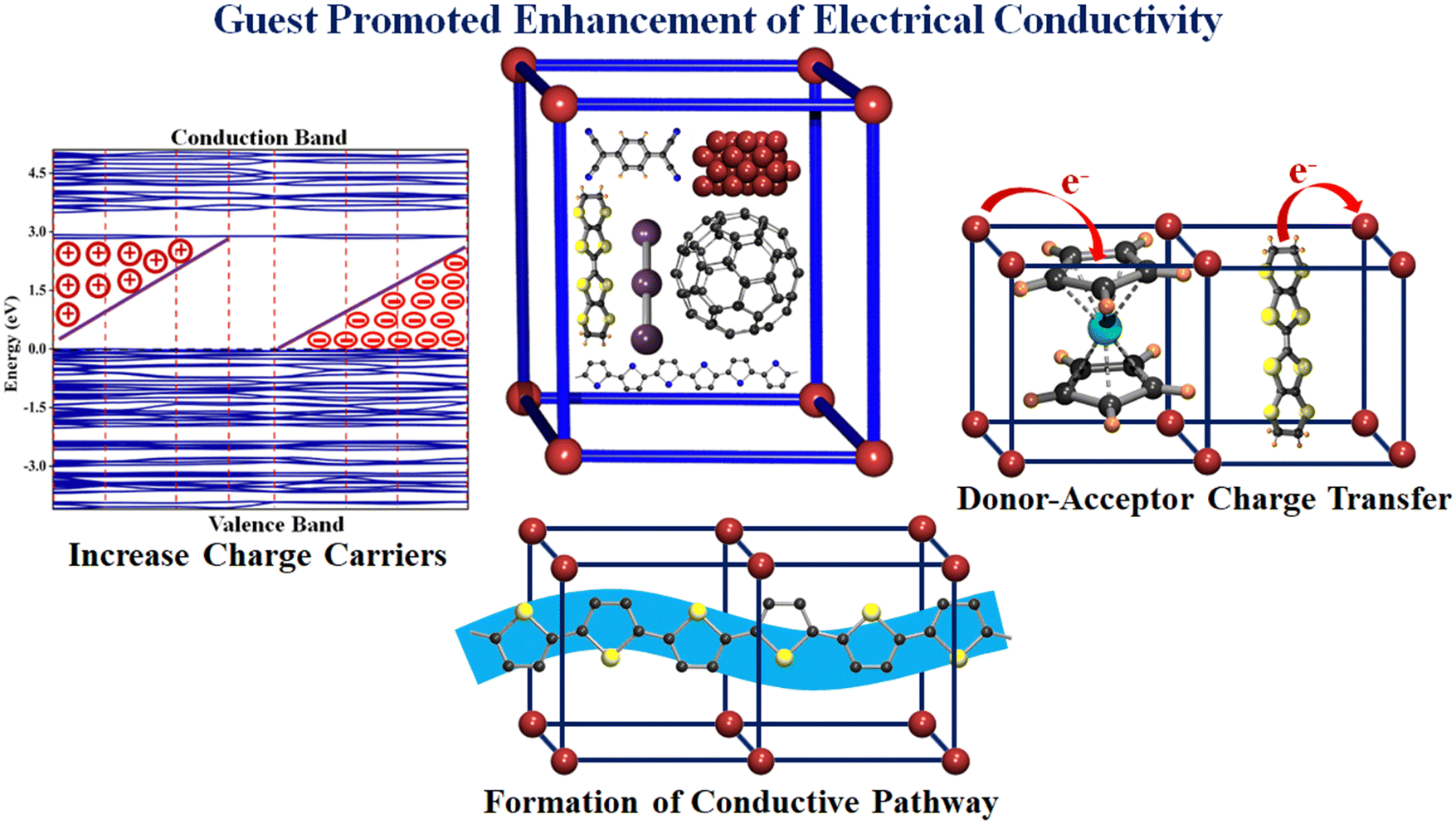 | ||
| Fig. 1 Different mechanisms to promote and enhance electrical conductivity in porous MOFs/PCPs by encapsulation of different guest species. | ||
Herein, we present an exhaustive review of the characteristics of the guest species that have been used by different research groups to enhance the charge transport properties of MOFs. We start with the charge transport mechanisms (band and hopping transport) operative for these MOFs and with the different charge transport pathways: (a) through bond, (b) through layer, (c) through space, (d) redox hopping and (e) through guest. We then provide an overview of the formation of host–guest MOF structures through encapsulation of guest species by both in situ and post-synthetic modification methods. We present the principles that guide the choice of electroactive guest species to design ec-MOFs. Afterward, we show examples of guest-dependent electrical conductivity in MOFs revising all the guest species used to enhance charge transport in MOFs (organic60 and inorganic61 molecules and organic conducting polymers63). According to their composition, structure, host–guest interaction and charge conducting behaviour, we classify these guest species into three categories: (a) metal-based guests35 (metal ions, metal nano-clusters and metal oxides), (b) molecule-based guests (TCNQ, iodine and polyiodides, ferrocene, fullerene, tetrathiafulvalene and its derivatives, metal–organic molecules, bromine, organo-metallic compounds, etc.) and (c) organic conducting polymer guests (such as PEDOT, PANI, PPy, PA and PTh) (Scheme 1). We discuss the different methods for the encapsulation of the guest species, the modification of the geometry of the framework after guest encapsulation, the charge transport pathway, the operative charge transport mechanism and the enhancement/change of electrical conductivity of the resulting guest-loaded host MOFs. Afterward, we discuss the different methods employed to develop thin films of MOFs to find out the most suitable ones for the extrinsically conducting MOFs. We have classified all the processes into two categories based on the medium used for the thin film preparation: (a) liquid phase processing (including exfoliation, electrochemical synthesis, interfacial method, epitaxial growth, etc.) and (b) gas phase processing (physical vapor deposition, atomic layer deposition and chemical vapor deposition). Then, we discussed different applications like electrocatalysis, sensing, charge storage, photoconductivity, photocatalysis, etc. using ec-MOFs. Finally, we have summarized the general aspects of this field, obstacles and perspectives. We have not considered those guest species which can’t be accommodated within the pores of MOFs.
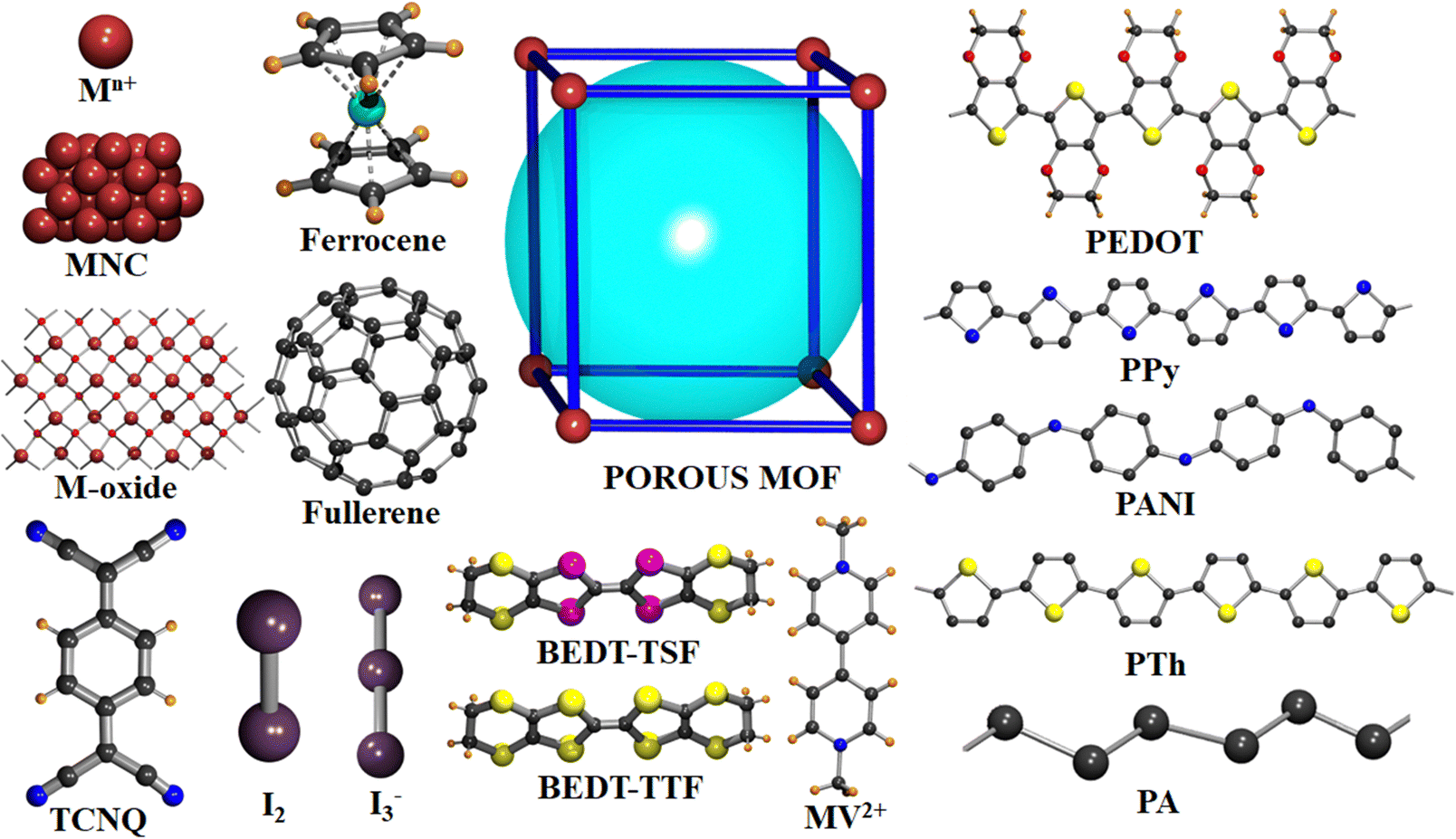 | ||
| Scheme 1 Different types of dopants used to modulate the electrical conductivity of MOFs. | ||
1.1 Transport mechanisms
Charge transport in conductive MOFs usually takes place through two types of mechanisms: (i) band-like and (ii) redox-hopping (Fig. 2).64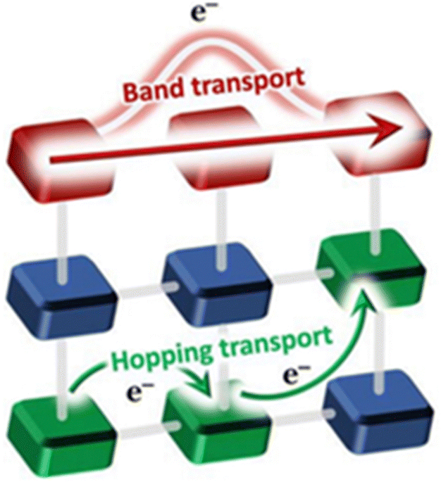 | ||
| Fig. 2 Band-like and redox hopping conductivity mechanisms operating in MOFs. Reproduced with permission from ref. 64. Copyright 2019, Royal Society of Chemistry. | ||
(i) Band transport occurs when the strong overlap between the metal and ligand orbitals of the MOFs generates continuous energy valence and conduction bands. The energy difference (Eg) between these bands defines their predictable electrical properties like metallic conductors (when both bands overlap and Eg = 0), semiconductors (when Eg < 3.6 eV), and insulators (when Eg ≥ 3.6 eV).65 For metallic conductors, both the conduction and valence bands merge and they show a decrease in conductivity with increasing temperature due to electron–phonon coupling which restricts the free movement of electrons in the band. In semiconductors, the electrical conductivity increases with increasing temperature due to the increase in charge carriers in the conduction band. For a classical semiconductor, the conductivity follows the Arrhenius law: σ = σ0![[thin space (1/6-em)]](https://www.rsc.org/images/entities/char_2009.gif) exp(−Ea/kT) where Ea is the activation energy, which is equal to half of the band gap (Ea = Eg/2). In insulators, there should not be any change in the electrical conductivity when the temperature is varied.
exp(−Ea/kT) where Ea is the activation energy, which is equal to half of the band gap (Ea = Eg/2). In insulators, there should not be any change in the electrical conductivity when the temperature is varied.
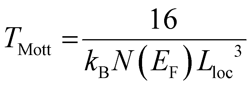
(ii) Hopping transport assumes that the charges are localized and “jump” through a phonon-assisted quantum tunnelling mechanism. In this case, the conductivity follows the equation σ = σ0exp [(−T0/T)α], where α = 1/(1 + d) and d is the dimensionality of the conducting lattice. Thus, α = 1/4 for three-dimensional (3D) lattices, as predicted by the Mott model.66 In this case, the electron transport can be described as an exchange process between redox couples. In this hopping model, when the temperature increases, the electron delocalization increases, and, therefore, the conductivity also increases. The electrical conductivity can be defined by Mott's variable range hopping (VRH) theory (eqn (1)):
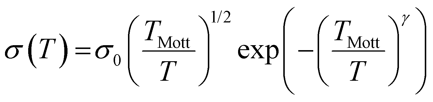 | (1) |
 | (2) |
| MOF | Guest | Methoda | σ MOF (S cm−1) | σ Guest@MOF (S cm−1) | σ mechanism | Ref. |
|---|---|---|---|---|---|---|
| a PSM, post-synthetic method. b BT, band transport. | ||||||
| Mg-MOF-74 | 0.35LiOiPr + 0.25LiBF4 | PSM | — | 3.1 × 10⁻⁴ | Hopping | 69 |
| Mg-MOF-74 | 0.05LiBF4 | PSM | — | 1.8 × 10⁻⁶ | Hopping | 69 |
| Mg-MOF-74 | 0.6LiOiPr | PSM | — | 1.2 × 10⁻⁵ | Hopping | 69 |
| UiO-66 | Li-OtBu | PSM | — | 1.8 × 10⁻⁵ | Hopping | 70 |
| [Cu2(BPY)2(DSNDI)] | LiClO4 | PSM | 4.65 × 10⁻¹² | 2.3 × 10⁻⁶ | Hopping | 71 |
| [Zn(OBA)(L)·DMF] | Cd2+ | PSM | 5.8 × 10⁻⁶ | 1.8 × 10⁻² | Hopping | 72 |
| Rb-CD-MOF | AgNC | PSM | 6.8 × 10⁻¹⁰ | 3.1 × 10⁻⁹ | Hopping | 73 |
| NU-1000 | AuNP | PSM | ≤10−12 | 5.2 × 10⁻⁷ | Hopping | 74 |
| NU-1000 | SnO2 | PSM | ≤10−12 | 1.8 × 10⁻⁷ | BT | 75 |
The electron conduction in both, ic-MOFs and ec-MOFs, proceeds through different pathways like through bond, through layer, through space and redox hopping.35 However, electron transport may occur only through guest species in some ec-MOFs (as we will see later, there are many insulating MOFs that become conductive only when the guests are inserted). In through-bond transport, the metal–ligand overlap is the predominant factor in promoting the electron transport. Based on this transport idea, several ligands with soft donor atoms (S, P, Se, etc.) have been combined with different transition metal ions to construct conductive MOFs.46 Following the electron transport in 2D materials like graphene, the design of conductive MOFs with extended π-conjugated organic ligands (like benzene, triphenylene, coronene, etc.) has gained much attention. Note that in these MOFs, the electron transport follows a through-plane pathway.47 Interlayer π-interactions have also significant contribution in through-space charge transport for these 2D layered MOFs. The π-interactions operative between the aromatic core of organic ligands can transport electrons through the MOF as well as through space. Encapsulation of aromatic guest molecules within the void space of MOFs can promote the through space charge transfer between the aromatic cores of the organic building blocks of the host framework.35 Utilization of redox-active metal ions48 or ligands49 or guest species62 may induce the charge transport within the framework thanks to the hopping of localized electrons between different redox active sites. Finally, the encapsulation of organic conductive polymers within the void space of host frameworks induces electron conduction in the MOF through the polymeric chains of the guest.63 In some cases, the guest–guest interaction is also operative to conduct electrons within the host framework.
1.2 Host–guest MOFs
In MOF literature, a host–guest complex is defined as a chemical system made up of two or more subunits self-assembled together to form a super-molecular entity. In a host–guest complex, there is a control of the host–guest interactions and the guest (usually a molecule) is encapsulated within the continuous structure of the host.76–78 Different types of intermolecular interactions like hydrophobic association,79 hydrogen bonding,80 electrostatic interactions,81 metal coordination,82 van der Waals forces,83 π–π stacking interactions,84etc. have been found to stabilize the host–guest structure. Within the confined space of the host, the geometry, molecular orientation, supramolecular behaviour and subsequent properties of the guest molecules may be different from those in the bulk and gas phases. On the other hand, the structure-related functionalities of the host–guest complex can be modulated by changing the type and amount of the inserted guest. Different types of molecular systems having discrete inner cavities such as crown ethers,85 cryptands,86 cavitands,87 calixarenes,88etc. have been designed for tailor-made functionalities through encapsulation of different types of guests.Different well-established methods have been used by researchers to load guest molecules within the host MOFs. These methods can be grouped into two main categories: (a) templated in situ (TIS) and (b) post-synthetic modification (PSM).
In the TIS method, the guest species are mixed with the metal ions and the ligands during the MOF synthesis. The strong metal–ligand coordination interactions build the framework architecture around the guest molecules. The guest molecules remain in the channels and cavities anchored by weak interactions, coordinated to unsaturated metal centres or even connected to functional groups of the ligands. These guest molecules, as templates, may induce a different structure of the MOFs compared to the one obtained in the absence of these guest species. Such TIS synthesis allows the preparation of single crystals of guest-encapsulated host structures to study the host–guest interactions. This method also allows encapsulation of guests larger than the pore window of the framework that restricts the removal/insertion of the guests. Different electroactive molecules like iodine, TTF, etc. and monomers of different organic conducting polymers have been incorporated within the void space of MOFs by this method (Fig. 3).
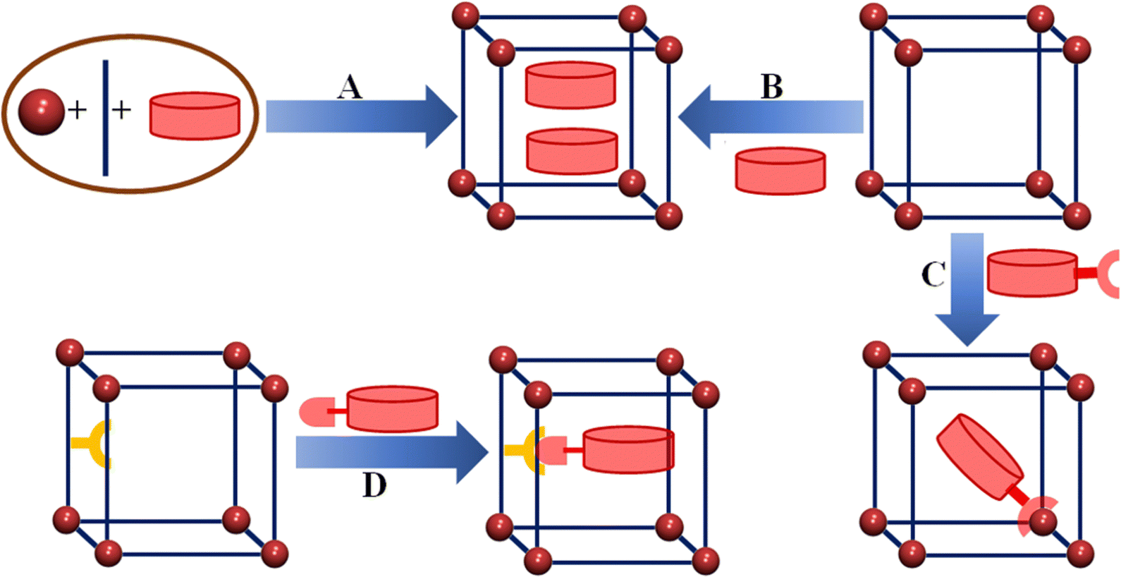 | ||
| Fig. 3 Different encapsulation methods to prepare guest@host MOF structures: (A) template method, (B) post-synthetic encapsulation, (C) grafting on metal and (D) grafting on the ligand. | ||
Post-synthetic modification is a well-established method to change the basic structure of the synthesized MOFs to obtain desired functionalities. Different guest molecules or guest precursors can be inserted within the channels or pores of MOFs. Researchers have used different techniques for guest loading such as dissolving the guest in different solvents, adsorption of guests in the gas phase, ion exchange, etc. Encapsulation of guests through this PSM method depends on the size of the guest, pore window size of the host and host–guest interactions. Though this method is very easy to handle and used very often, it has several drawbacks: (i) loss of crystallinity during guest encapsulation, (ii) inhomogeneous distribution of the guests within the MOF channels and (iii) leaching. In several cases, post-treatment of encapsulated precursors to build the active guest species can damage the crystallinity of the frameworks.
Besides these two popular methods, another method namely grafting within the MOF architecture has also gained popularity. In this method, the framework is pre-functionalized either by using open metal sites or ligands having free functional organic sites, which are further utilized to load the guest species following the pre-functional sites. The accommodated guest species have been found to attach strongly to the free functional organic sites.
1.3 Principles for the choice of guests to design ec-MOFs
Electron conduction in MOFs may follow two different transport pathways: (a) through-bond and (b) through-space (Fig. 4).35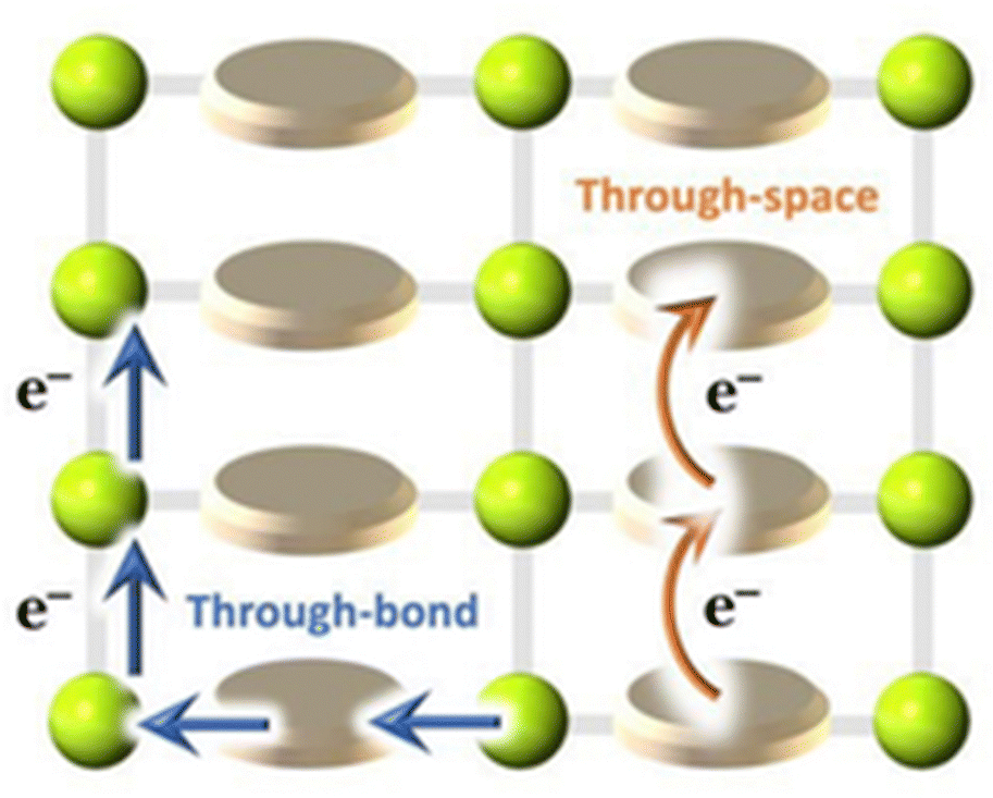 | ||
| Fig. 4 Through-bond and through-space charge-transport pathways in MOFs. Reproduced with permission from ref. 64. Copyright 2019, Royal Society of Chemistry. | ||
The through-bond charge transport implies the presence of infinite metal–ligand coordination interactions in the MOF to conduct electrons. A good d–p (σ or π) overlap between metal orbitals and ligand functional groups with well-matched energy levels leads to small band gaps and high charge carrier mobilities. On the other hand, for the through-space charge transport, electron conduction occurs through the non-covalent π-interactions between highly conjugated planar organic moieties.
In contrast, for extrinsically conducting MOFs, electron conduction is dependent on the guest molecules and host–guest interactions. In the previous section, we have discussed the incorporation of guest species within the host MOFs where the host–guest binding may vary from covalent (including coordination) bonding to non-covalent interactions. Additionally, the incorporation of organic conductive polymers can show charge transport without any significant influence on the framework.
Based on this well-known host–guest interaction, the ec-MOFs can be designed following four different strategies: (i) MOF–guest coordination interactions: the encapsulated guest moieties can coordinate metal centres to promote the electrical charge transport pathway within the framework, as observed by Allendorf et al., who have shown a 1010 times enhancement of the electrical conductivity of HKUST-1 through encapsulation of TCNQ.89 The encapsulation of a secondary bridging moiety provides an alternative pathway for the charge transport for the weakly conducting or insulating MOFs through well-matched metal–guest orbital overlaps. After the first report, several groups have attempted to modify the charge transport behaviour of MOFs through encapsulation of different types of charge-carrying organic bridging ligands like TCNQ and related molecules.90 (ii) Donor–acceptor interactions: the donor–acceptor interactions between the host MOF and guest moieties have been exploited to develop ec-MOFs. In this case, the guest moiety can be grafted on the metal–organic structure or within the void space. Hupp et al. have shown the enhancement of electrical conductivity through encapsulation of fullerene moieties within the void space of a MOF.91 (iii) Extended π-interactions: the encapsulation of aromatic guest species may help to develop extended host–guest charge transport pathways.92 (iv) Conducting polymers: organic conductive polymers like PPy, PANI, etc. can provide an independent conducting pathway and, therefore, the incorporation of organic conducting polymers within the void space of MOFs is an excellent strategy for developing ec-MOFs.93,94
2. Classification of guests to design extrinsically conducting MOFs
Electrical conductivity of a material is defined as the charge transport ability through the material and is characterized by both the charge carrier concentration and the charge carrier mobility. It is highly challenging to control the charge transport properties of MOFs. However, chemical modifications may modulate the electrical conductivity of the MOFs in a controlled way. In the present review, we focus only on the modulation of the electrical conductivity of MOFs by guest encapsulation within the channels or cavities i.e., extrinsically conductive MOFs (ec-MOFs).Self-assembly of carboxylate-containing organic ligands with metal ions results in poor metal–ligand overlap with large energy gaps and poor conductivity.95 Additionally, the presence of inherent porosity cuts off the extended π-conjugation among the aromatic ligands of the framework. In this respect, encapsulation of electroactive guest species within the channels or cavities of these MOFs can build up an alternative charge transport pathway throughout the framework.96 The charge transport of such guest-encapsulated MOFs follows two different mechanisms: (a) host–guest charge transfer interaction and (b) charge transport through the guest. The presence of discrete guests within the pores of MOFs may enhance the first mechanism resulting in an increase of the electrical conductivity through host–guest charge transfer interactions. In contrast, conducting polymers enhance the second mechanism since they provide extended conjugation assemblies throughout the MOF as a charge transport pathway.97,98 In some cases, a guest–guest charge transfer interaction has also been found.99 To date, many studies have been done on this topic and, herein, we summarize all these efforts to construct extrinsically conducting MOFs by guest insertion. Thus, in this review, we present the design of conductive MOFs based on the encapsulation of different types of guests within the voids or channels.
To date, several types of guest species like metal ions, metal nanoparticles, metal oxides, inorganic and metal–organic complexes, different organic molecules, halogens, anions, organic polymers and so on, have been accommodated within the void space of MOFs, following the dimension of the pores and understanding the host–guest interactions. In the present review, to discuss the modulation of electrical conductivity of porous MOFs through encapsulation of guest species, we have classified the guests into three categories: (i) metal-based guests, (ii) molecule-based guests and (iii) conducting polymers. This classification is based on their chemical composition, geometry, host–guest interaction and charge transport pathway.
In the first category, metal-based guests, we include metal ions, metal nanoparticles (MNPs) and metal-oxides, as the main component of these guests is the metal ion itself. Metal ions may be present in the pores either as a single metal ion or as a cluster attached to the framework by electrostatic interactions or coordination bonds. An example of this type is the incorporation of Cd2+ ions within a framework through Cd2+⋯S interaction of the ligand.72 MNPs may agglomerate within the pores of the MOFs through electrostatic interaction. Thus, Ag+ ions can be loaded within the Rb-CD-MOFs through electrostatic interactions between the metal ions and hydroxide groups that also serve to reduce Ag+ to form Ag-NPs.73 In a similar way, metal-oxides can be incorporated into MOFs through electrostatic interactions with the hydroxide groups of the framework.75 In the second group of guests, molecules and molecular entities, we will discuss different types of inorganic molecules like ferrocene, nickel(II)carbolide complexes, iodine/polyiodides, etc. as well as organic molecules like TCNQ, fullerene, TTFs, etc. These molecules or molecular entities have their own molecular structure and are loaded within the framework through different host–guest interactions, depending on the framework and the guest. Their charge transfer pathways may also vary with the guest. In the third group of guests, organic conductive polymers, we include well-known conductive organic polymers like PEDOT, PPy, PANI, etc. that have 1D structures formed by a purely organic backbone and interact with the host framework mostly through π-interactions.
2.1 Metal-based guests
Encapsulation of different metal-based guest species within porous MOFs has gained much attention in promoting different physical and chemical properties of the host framework. Thus, Bu et al. have demonstrated how the encapsulation in MOFs of different metal-based guest species can modulate their catalytic, sensing and luminescent properties.24 Of course, metal-based guests have also been often used for the enhancement of electrical conductivity of MOFs. Based on their composition, we have classified these metal-based guests into three main sub-categories: (a) metal ions, (b) metal nano-particles (MNPs) and (c) metal oxides. Such metal-based guest species help to promote the charge transfer within the guest@host MOF through electrostatic interactions and a redox hopping mechanism.Long et al. measured the electrical conductivity of the Li+ doped Mg-MOF-74 formulated as {(LiOiPr)0.35(LiBF4)0.25(EC)(DEC)}@Mg2(dobdc) (Table 1) (H4dobdc = 2,5-dihydroxy-benzene-1,4-dicarboxylic acid, EC = ethylene carbonate and DEC = diethyl carbonate, Fig. 5).69
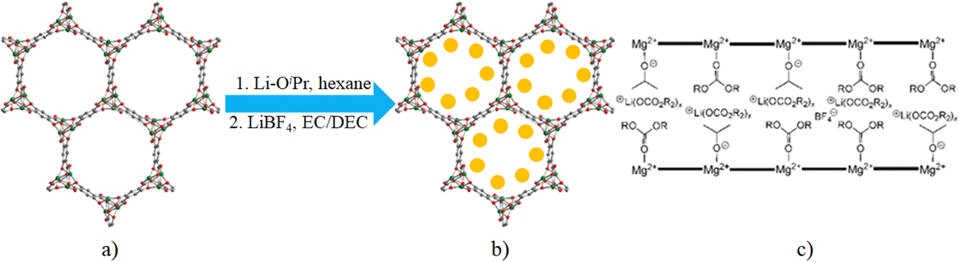 | ||
| Fig. 5 (a) Structure of Mg-MOF-74. (b) Li+ incorporation in Mg-MOF-74 (Li+ = yellow balls). (c) Representation of a cross-sectional view along a channel of the solid [R = CH2–CH2 (EC) or CH2CH3 (DEC)]. Reproduced with permission from ref. 69. Copyright 2011, The American Chemical Society. | ||
Mg-MOF-74 contains coordinatively unsaturated Mg2+ centres upon desolvation. Desolvated Mg-MOF-74 was immersed in a hot hexane solution of LiOiPr for 2 weeks and the obtained material (LiOiPr)0.5@Mg2(dobdc) was immersed in a 1 M solution of LiBF4 in 1:1 EC/DEC to obtain the compound {(LiOiPr)0.35(LiBF4)0.25(EC)(DEC)}@Mg2(dobdc). Electrical conductivity was measured by the two-probe contact method on pressed pellets. This compound shows an electrical conductivity of 3.1 × 10⁻⁴ S cm−1, higher than that of the related compounds {(LiBF4)0.05(EC)x(DEC)x}@Mg2(dobdc) (1.8 × 10⁻⁶ S cm−1) and (LiOiPr)0.6@Mg2(dobdc) (1.2 × 10⁻⁵ S cm−1). Ethylene carbonate molecules and OiPr− anions coordinate to the Mg2+ sites which consequently allow the penetration of charge-compensating Li+ ions within the channels. The Li+ ions can easily move along the channels resulting in the observed conductivity enhancement. These authors have also investigated the conductivity of LiOMe and LiOEt incorporated within Mg-MOF-74 but these are worse conductors than the other compounds.69 The same group has also reported an increase in the electrical conductivity of UiO-66 {[Zr6O4(OH)4(BDC)6]} in a similar way. Dehydration of the framework creates open coordination sites on the Zr4+ ions by forming {Zr6O6}12+ core units. Immersion of the dehydrated UiO-66 in a 1 M LiOtBu solution in THF at 353 K for 7 days leads to compound Li-OtBu@UiO-66 whose AC impedance measurement shows a conductivity of 1.8 × 10⁻⁵ S cm−1 at room temperature.70
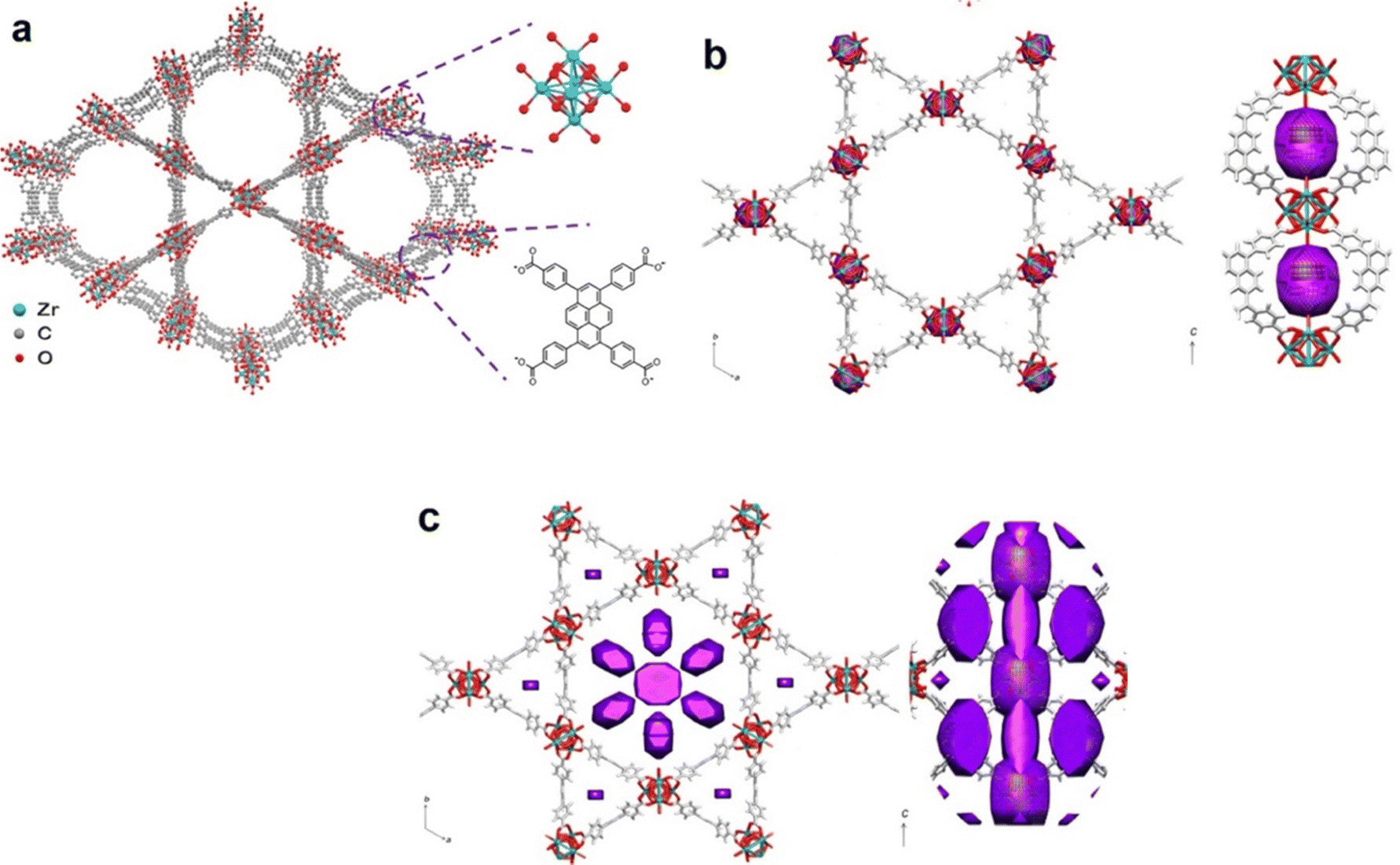
Recently, Saha et al. have prepared a 2D neutral Cu(I)–sulfonate MOF using a NDI ligand functionalized with two sulfonate groups (NDIDS = 4,4′-(1,3,6,8-tetraoxobenzo[lmn][3,8]-phenanthroline-2,7(1H,3H,6H,8H)-diyl)-bis(2-hydroxy benzoic acid)), which can simultaneously bind guest Li+ cations with the carbonyl groups and with the free sulfonate oxygen atoms and the perchlorate anions through anion–π interaction with the π-acidic NDI core. The impedance measurement shows that Li+@MOF has 106 times higher conductivity (2.3 × 10⁻⁶ S cm−1) than the undoped sample (4.65 × 10⁻¹² S cm−1).71
In the same year, the Morsali group showed an interesting case of modulation of the electrical conductivity of a porous framework through Cd2+ adsorption. Following the Cd2+ uptake capacity of the amine-functionalized UiO-66 framework, these authors prepared a MOF formulated as [Zn(OBA)(L)]·DMF (where L = 5,6-di(pyridin-4-yl)-1,2,3,4-tetrahydropyrazine and H2OBA = 4,4′-oxybisbenzoic acid). The basic building block N1,N2-bis(pyridin-4-ylmethylene)ethane-1,2-diamine undergoes a C–C coupling reaction and forms L under the reaction conditions. Structural analysis shows that [Zn2(COO)4] paddle-wheel units are connected by OBA ligands to form coordination layers which are further connected by L to form a 2-fold interpenetrated 3D framework containing channels decorated by amine groups (Fig. 6). The activated framework was soaked in an aqueous solution of Cd(NO3)2 for 10 min and the absorbed amount was determined by ICP analysis. The absorption capacity is 155 mg g−1. Interestingly, the framework shows selective absorption of Cd2+ over Hg2+, Pb2+, Cd2+, Zn2+, Co2+, Cr2+, Fe2+ and Ca2+ under similar conditions. The unusual selective absorption of Cd2+ within the framework is proposed to be based on weak interactions between the absorbed Cd2+ with the amine and pyrazone groups of the ligand. The electrical conductivity of the framework increases from 5.8 × 10⁻⁶ S cm−1 to 1.8 × 10⁻² S cm−1 after Cd2+ incorporation and the electrical conductivity is dependent on the amount of absorbed Cd2+ ions. The enhancement of electrical conductivity arises from the redox hopping between the dopant and the host framework.72
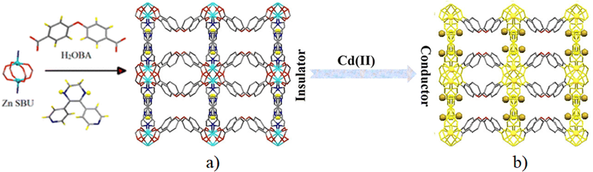 | ||
| Fig. 6 (a) Representation of the 3D framework of MOF [Zn(OBA)(L)]·DMF formed by the interaction of the paddle-wheel Zn2(CH3COO)4 secondary building unit, H2OBA, and L ligand. (b) Possible pathway for electron transfer (yellow) of Cd@MOF. (The golden balls display the Cd2+ ions). Reproduced with permission from ref. 72. Copyright 2019, The American Chemical Society. | ||
The first report, by Han et al., showed an enhancement of the electrical conductivity of an insulator MOF, Rb-CD-MOFs, formed by reacting RbOH with γ-cyclodextrin (γ-CD).73 Single crystals of the MOFs were immersed in an acetonitrile solution of AgNO3. Ag+ ions diffused within the channels of the MOF and were reduced by the –OH groups of the cyclodextrin molecules to form Ag nanoclusters (AgNCs). X-ray powder diffraction (XRPD) studies show that AgNC@Rb-CD-MOF does not lose any crystallinity while TEM analysis indicates that the size of the AgNC is ∼2 nm. N2 adsorption study indicates that compound AgNC@Rb-CD-MOF has a high porosity, similar to the parent MOF. Two-probe electrical conductivity measurements show that the conductivity of this compound varies in the range of 6.8 × 10⁻¹⁰ to 3.1 × 10⁻⁹ S cm−1, whereas the parent Rb-CD-MOF is an insulator. Furthermore, upon illumination, AgNC@Rb-CD-MOF shows a further 104 times enhancement of the electrical conductivity.73 In this case, the charge transport occurs through the hopping mechanism (Fig. 7).
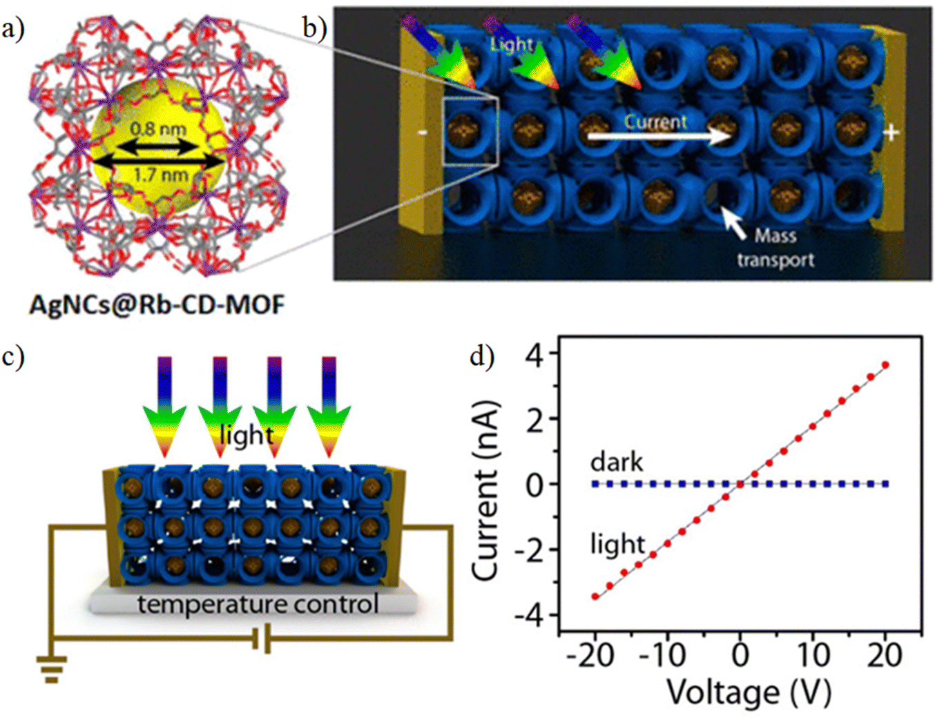 | ||
| Fig. 7 (a) Unit cell content of an Rb-CD-MOF crystal synthesized from γ-CD and RbOH. The yellow sphere indicates a ∼1.7 nm cavity; the channels connecting the cavities are ∼0.8 nm wide. (b) Schematic representation of Ag nanoclusters deposited by immersing Rb-CD-MOF crystals in a CH3CN solution of AgNO3. Not all the cavities contain nanoclusters. (c) Experimental arrangement for measuring photoconductance of MOF crystals. (d) I–V characteristics of AgNC@Rb-CD-MOF crystals under light irradiation (630 mW cm−2) and in the dark. The conductivities are, respectively, 1.8 × 10⁻⁸ and ∼2 × 10⁻¹¹ S cm−1. Reproduced with permission from ref. 73. Copyright 2015, The American Chemical Society. | ||
A similar strategy was used by Ma and co-workers to prepare AgNC@Pb-CD-MOF.100 Pb-CD-MOF, prepared by reacting PbCl2 with β-CD, was taken in ultrapure water and AgNO3 was added to the solution. Ag+ ions diffuse in the channels and are then reduced by the –OH groups of the β-CD moieties to form AgNCs. Impedance analysis shows that AgNC@Pb-CD-MOF shows better conductivity than the parent MOF Pb-CD-MOF, as the incorporation of AgNC has improved the electron transfer ability. AgNC@Pb-CD-MOF was further used for electroluminescent based immune-sensing.100
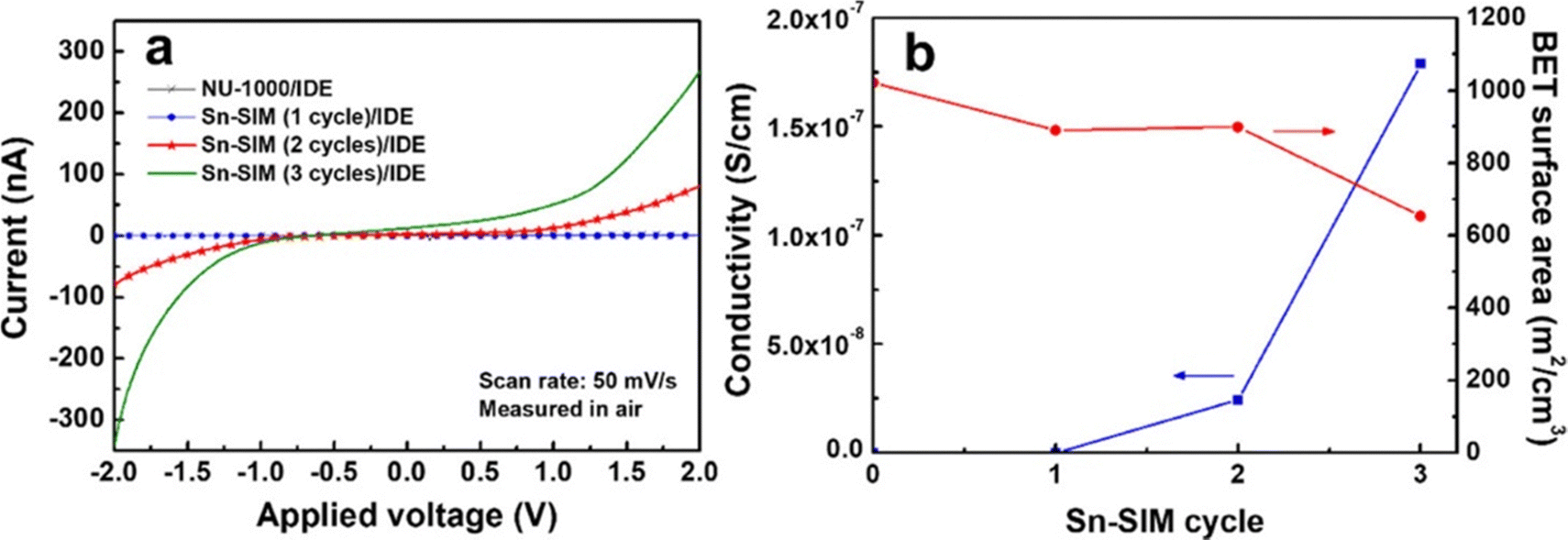
A significant enhancement of the electrical conductivity upon incorporation of AuNP within the pores of NU-1000 MOF has been recently reported by Saha and co-workers.74 For the first time, they have loaded AuNPs within MOF pores by directly immersing NU-1000 MOF crystals in aqueous AuCl3 solution overnight. The consequent reduction of Au3+ to Au-NPS was monitored by the naked eye colour change from bright yellow to orange. The reduction of infiltrated Au3+ ions was carried out by hydroxide groups of the [Zr6(μ3-O)4(μ3-OH)4(OH)4(H2O)4] nodes of the framework (Fig. 8).
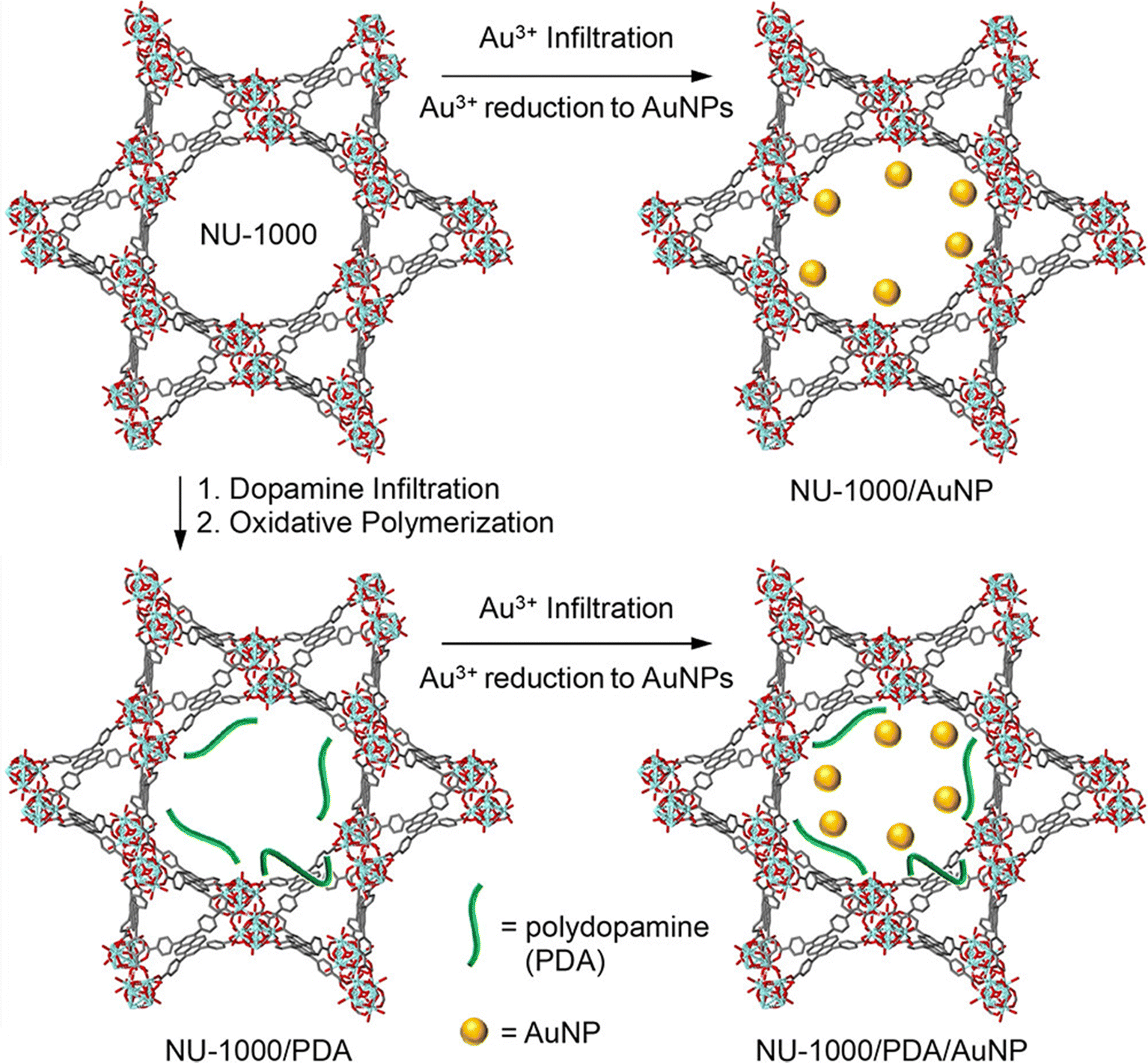 | ||
| Fig. 8 Transformation of NU-1000 to AuNP@NU-1000, PDA@NU-1000 and (AuNP-PDA)@NU-1000 MOFs. Reproduced with permission from ref. 101. Copyright 2018, The American Chemical Society. | ||
The formation of AuNP@MOF was characterized by XRPD analysis. In order to compare the formation of AuNP@MOF, they have also attempted to synthesize AuNP within the pores of NU-1000 MOF using a multi-step method developed by others.101 This method implies (a) incorporation of dopamine monomers within the pores of the MOF, (b) polymerization of the dopamine monomers to obtain PDA within the MOF pore, (c) immersion of PDA@MOF in an aqueous solution of AuCl3 and the consequent reduction of Au3+ by the hydroxide groups of the dopamine moieties to form (AuNP–PDA)@NU-1000 MOF. The XRPD analysis indicates the formation of AuNPs within the pores of the NU-1000 MOF without loss of any crystallinity, resulting in a similar MOF as the one synthesized directly without the help of dopamine. N2 sorption studies indicate that the BET surface area of AuNP@NU-1000 MOF (1527 m2 g−1) is higher than that of AuNP–PDA@NU-1000 MOF (715 m2 g−1) but lower than the parent MOF (2215 m2 g−1). These values clearly probe the loading of AuNPs and PDA within the pores of the framework.
Two-probe electrical conductivity measurements show similar room-temperature conductivities of 1.2 × 10⁻⁷ S cm−1 for AuNP@NU-1000 MOF and 5.2 × 10⁻⁷ S cm−1 for AuNP–PDA@NU-1000 (Fig. 9), both 104 times higher than that of the parent MOF (≤10−12 S cm−1). It is suggested that the charge hopping or tunnelling of electrons across the framework becomes more facile after the incorporation of AuNPs.74
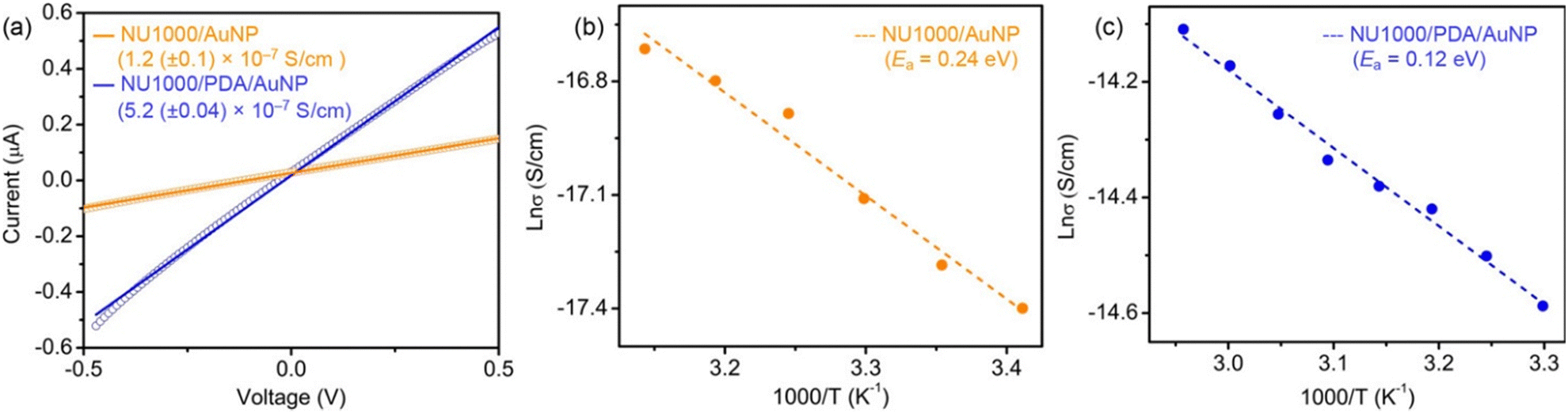 | ||
| Fig. 9 (a) Representative I–V plots of AuNP@NU-1000 (orange) and (AuNP–PDA)@NU-1000 (blue). (b) Arrhenius plots of the temperature dependent conductivities of AuNP@NU-1000 (orange) and (AuNP–PDA)@NU-1000 (blue), showing their respective activation energies. Reproduced with permission from ref. 101. Copyright 2018, The American Chemical Society. | ||
Recently, Vilian et al. have inserted Pd-NPs into MIL-101(Cr) to obtain Pd@MIL-101(Cr), based on the interaction between the uncoordinated amine groups with the loaded Pd centres.102 The synthesized MIL-101(Cr) MOF was soaked in an aqueous solution of PdCl2 at room temperature for 8 h and afterward the solid was collected by centrifugation. Pd nanoparticles were formed by reduction using H2 at 200 °C for 1 hour. Impedance analysis indicates that the charge transfer resistance (Rct) of Pd@MIL-101(Cr) (384 Ω) is much lower than that of the parent MOF (1104 Ω).102
Gold nanoparticles have also been loaded, by Wang et al., into the void space of an imidazole-based framework formulated as [Zn2(mim)4(Hmim)(H2O)3] (ZIF-L) (Hmim = 2-methylimiazole, ZIF = zeolitic-imidazolate framework). The impedance analysis also shows that the charge transfer resistance of Au@ZIF-L is much lower than that of ZIF-L itself.103
Platinum nanoparticles can also be incorporated into three different UiO-MOFs (namely, UiO-66, UiO-67 and UiO-68), as shown by Guo and co-workers.104 The Pt-NPs were incorporated by in situ synthesis and characterized using TEM, XRPD, XPS and N2 adsorption analyses. XRPD analysis shows that the crystallinity of UiO-66 and UiO-68 does not change upon loading with Pt-NPs while the crystallinity of UiO-67 is significantly damaged. Interestingly, Pt-NP@UiO-66 and Pt-NP@UiO-68 show better adsorption behaviours and larger surface areas than their parent frameworks. Impedance analysis indicates that the electron transfer ability increases significantly for all the frameworks after Pt-NP loading. The charge transfer resistance (Rct) value increases as follows: Pt@UiO-66-2/GCE (2396 Ω), Pt@UiO-68-2/GCE (2677 Ω), UiO-66/GCE (3042 Ω), Pt@UiO-67-2/GCE (3379 Ω), UiO-68/GCE (4697 Ω) and UiO-67/GCE (5872 Ω).104
The host–guest structure, AgNC@ZIF-67, has been prepared by incorporating Ag+ ions within the framework and consequent reduction by NaBH4. Impedance spectroscopy shows that AgNC@ZIF-67 is a better conductor than ZIF-67 itself, indicating that the presence of AgNCs is an important factor for improving the conductivity of the material. Furthermore, the material was used for electrochemical glucose sensing.105 Similarly, Dong et al. have developed a silver nanoparticle MOF: Ag@ZIF-67 that is more conductive than the pristine framework.106
Very recently, Ballav and co-workers have shown the possibility of tuning the electrical conductivity of the semiconducting MOFs [Cu3(HHTP)2] and [Cu-TCNQ] through encapsulation of AgNPs.107 Thin films of these MOFs and the corresponding AgNP@MOFs were prepared on fluorine-doped tin oxide (FTO) substrates through the layer-by-layer (LBL) method. The film thickness was monitored by the LBL cycles while the doping of AgNPs was varied with the exposure time in AgOAc solution. The formation of AgNP@MOFs was monitored using XRPD, FESEM, EDXS and XPS studies. The electrical conductivity measurements show that [Cu3(HHTP)2] is a semiconductor with an electrical conductivity value of ∼10−6 S cm−1. The conductivity value increases with the doping of AgNPs. Doping for 5 minutes can enhance the electrical conductivity by ∼2 orders of magnitude, although it still remains semiconducting. In contrast, doping for 10 minutes and above results in AgNP@[Cu3(HHTP)2] that shows a metallic behaviour with a conductivity value of ∼2 × 10⁻¹ S cm−1 at 300 K. On the other hand, the encapsulation of AgNPs within Cu-TCNQ in AgNP@Cu-TCNQ enhances its electrical conductivity by about 1000 times (from ∼7 × 10⁻⁷ to ∼4.7 × 10⁻⁴ S cm−1), although it shows a semiconducting behaviour. These authors have demonstrated that the formation of large amounts of Ag(0)-NPs within [Cu3(HHTP)2] is the main reason for such metallic conductivity of AgNP@[Cu3(HHTP)2] while Ag(I)-TCNQ is formed in the case of Cu-TCNQ.107
 | ||
| Fig. 10 (a) Top-view of the crystal structure of NU-1000. H-atoms are omitted for simplicity. DED maps of (b) SnO2@NU-1000 (1 cycle) and (c) SnO2@NU-1000 (3 cycles). The electron density of SnO2 is presented in purple. Reproduced with permission from ref. 75. Copyright 2018, The American Chemical Society. | ||
 | ||
| Fig. 11 (a) I–V curves of NU-1000/IDE, SnO2@NU-1000 (1 cycle)/IDE, SnO2@NU-1000 (2 cycles)/IDE and SnO2@NU-1000 (3 cycles)/IDE, measured in air at room temperature. (b) Electrical conductivity and BET surface area of NU-1000, SnO2@NU-1000 (1 cycle), SnO2@NU-1000 (2 cycles), and SnO2@NU-1000 (3 cycles). Reproduced with permission from ref. 75. Copyright 2018, The American Chemical Society. | ||
2.2 Molecule-based guests
Different types of electroactive molecules and molecular entities including TCNQ (7,7,8,8-tetracyanoquinodimethane), iodine, polyiodides, ferrocene, fullerene, tetrathiafulvalene and its derivatives, methyl viologen, etc. have been encapsulated within the channels of MOFs to induce and enhance conducting properties of the parent MOFs (Table 2). In most cases, the guest molecules are incorporated by post-synthetic methods within the voids of pre-synthesized MOFs, although, in some cases, guest molecules are used as templates and incorporated by in situ methods. The encapsulated guest species remain either attached to the metal/ligand framework by coordination/covalent linkages or within the voids through non-covalent interactions.| MOF | Guest | Method | σ MOF (S cm−1) | σ Guest@MOF (S cm−1) | σ mechanism | Ref. |
|---|---|---|---|---|---|---|
| L = biphenyl-3,3′′,5,5′′-tetracarboxylate; L1 = dicarbollide; PSM = post-synthetic method; TEMP = template; CT = charge transport; D–A CT = donor–acceptor charge transfer. | ||||||
| HKUST-1 | TCNQ | PSM | 10−8 | 7 × 10⁻² | CT | 89 |
| [Cu2(AcO)4(CuTPyP)1/2]·CHCl3 | TCNQ | PSM | 10−9 | 10−6 | CT | 90 |
| [Cu2(TATAB)3]·7.5H2O | TCNQ | PSM | 9.8 × 10⁻¹² | 10−7 | CT | 113 |
| [Zn3(DL-lac)2(pybz)2]·2.5DMF | I2 | PSM | — | 3.42 × 10⁻³ | D–A CT | 117 |
| [CoII3(lac)2(pybz)2]·2.7 I2 | I2 | PSM | — | 7 × 10⁻⁶ | D–A CT | 118 |
| Cu[Ni(pdt)2] | I2 | PSM | 10−8 | 10−4 | D–A CT | 119 |
| {[Cu6(pybz)8(OH)2]·I5−·I7−}n | I5− + I7− | PSM | — | 8.11 × 10⁻⁷ | D–A CT | 120 |
| [Cu6(pybz)8(OH)2]−(I−)2·3.5CH3OH | I− | PSM | — | 8.04 × 10⁻⁹ | D–A CT | 120 |
| [Co-NDC] | I2 | PSM | — | 1.88 × 10⁻⁶ | D–A CT | 121 |
| [Co1.5(BDC)1.5(H2bpz)]·0.5I2·DMF | I2 | PSM | 2.5 × 10⁻⁹ | 1.56 × 10⁻⁸ | D–A CT | 123 |
| [Tb(Cu4I4)(ina)3(DMF)] | I2 | PSM | 5.7 × 10⁻¹¹ | 2.16 × 10⁻⁴ | D–A CT | 124 |
| [VIII2(OH)2(L)] | I2 + I3− | PSM | 1.7 × 10⁻¹⁰ | 1.16 × 10⁻⁴ | D–A CT | 125 |
| Cu-TCNQ | I2 | PSM | 10−5 | 10−3 | D–A CT | 126 |
| [Cd(NDC)0.5(PCA)]·Gx | I2 | PSM | 10−12 | 10−7 | D–A CT | 190 |
| [Eu4(BPT)4(DMF)2(H2O)8] | In− | PSM | 8.27 × 10⁻⁷ | 2.71 × 10⁻⁵ | D–A CT | 127 |
| [Zn2(TTFTB)(H2O)2] | In− | PSM | 1.6 × 10⁻⁹ | 2.5 × 10⁻¹⁰ | D–A CT | 128 |
| [Zn3(ExTTFTB)2(H2O)4]·6EtOH | I2/I− | PSM | 10−10 | 10−6 | D–A CT | 131 |
| (BEDT-TTF)3[MnCr(ox)3] | BEDT-TTF | TEM | — | 250 | D–A CT | 137 |
| (BEDT-TSF)3[MnCr(ox)3]·CH2Cl2 | BEDT-TSF | TEM | — | 1–23 | D–A CT | 138 |
| (BEDT-TTF)x [MnRh(ox)3]·CH2Cl2 | BEDT-TTF | TEM | — | 13 | D–A CT | 139 |
| (BEDT-TTF)3[CoCr(ox)3] | BEDT-TTF | TEM | — | 1 | D–A CT | 140 |
| (BEDS-TTF)3[MnCr(ox)3] | BEDS-TTF | TEM | — | <10−6 | D–A CT | 140 |
| (BEDS-TTF)3[CoCr(ox)3] | BEDS-TTF | TEM | — | <10−6 | D–A CT | 140 |
| (BET-TTF)3[MnCr(ox)3] | BET-TTF | TEM | — | 4 | D–A CT | 140 |
| (BET-TTF)3[CoCr(ox)3] | BET-TTF | TEM | — | 21 | D–A CT | 140 |
| (BEDT-TSF)3[CoCr(ox)3] | BEDT-TSF | TEM | — | 2.3 | D–A CT | 140 |
| (BMDT-TTF)3[MnCr(ox)3] | BMDT-TTF | TEM | — | 1.5 | D–A CT | 140 |
| (ES(1Se)-TTF)3[MnCr(ox)3] | ES(1Se)-TTF | TEM | — | 0.1 | D–A CT | 140 |
| (BEDO-TTF)3[MnCr(ox)3] | BEDO-TTF | TEM | — | 1.4 | D–A CT | 140 |
| (BEDT-TTF)3[Cu(ox)3]3H2O | BEDT-TTF | TEM | — | 4 | D–A CT | 144 |
| (BEDT-TSF)3[Cu(ox)3]3H2O | BEDT-TSF | TEM | — | 140 | D–A CT | 146 |
| NU-901 | C60 | PSM | 10−3 | 10−14 | D–A CT | 91 |
| (TTFTB)3[(Fe3O)(H2O)2(OH)]2 | C60 | PSM | 3.7 × 10⁻¹¹ | 4.7 × 10⁻⁹ | D–A CT | 151 |
| HKUST-1 | Ferrocene | PSM | 10−14 | 2 × 10⁻⁹ | D–A CT | 166 |
| NU-1000 | [Ni(L1)2] | PSM | Insulator | 2.7 × 10⁻⁷ | D–A CT | 169 |
| [Zn2(TCPB)(BPDPNDI)] | MV2+ | PSM | 6 × 10⁻⁷ | 2.3 × 10⁻⁵ | D–A CT | 92 |
| [Zn2(TCPB)(BPDPNDI)] | DFDNB | PSM | 6 × 10⁻⁷ | 3.5 × 10⁻⁶ | D–A CT | 92 |
| [Zn2(TCPB)(BPDPNDI)] | DNT | PSM | 6 × 10⁻⁷ | 1.5 × 10⁻⁶ | D–A CT | 92 |
| Zn2TTFTB | TCNE | PSM | 10−7 | 120 × 10−7 | D–A CT | 202 |
| Cd2TTFTB | TCNE | PSM | 20 × 10−7 | 80 × 10−7 | D–A CT | 202 |
Such incorporation of electroactive molecules can induce or enhance the electrical conductivity by several mechanisms: (i) by creating a new electron conducting pathway throughout the framework thanks to the formation of covalent/coordination linkages between the metal centres, (ii) by developing a donor–acceptor (D–A) host–guest charge transfer pathway within the framework, and (iii) through guest–guest interactions.
In the first mechanism, the encapsulated guest acts as a bridge between metal centres and provides an alternative electron conduction pathway. It is obvious that the guest should be a good electronic conductor as TCNQ, which is a π-conjugated organic building block that may induce high conductivity through the formation of linkages between different metal centres of the MOFs. Similarly, the formation of polyiodide chains within the channels of MOFs can substantially enhance their electrical conductivity by formation of coordination bonds between metal centres and polyiodides. While the donor–acceptor (D–A) charge transfer interaction is a well-established phenomenon in co-crystals and has been used for applications in optoelectronic devices, it is less studied in MOFs. The formation of MOFs using metal–ligand coordination also reduces the electron density on the ligand backbone through the partial transfer of electron density from ligands to the cationic metal centres that act as electron acceptors. The incorporation of electron-rich guest species (iodides) within the voids/channels of MOFs produces donor–acceptor electron transfer pathways throughout the framework, inducing higher electrical conductivity. Again, the utilization of conjugated organic ligands for the synthesis of MOFs results in electron-rich skeletons, and therefore, the incorporation of electron acceptor molecules can also create D–A charge transfer pathways throughout the framework.
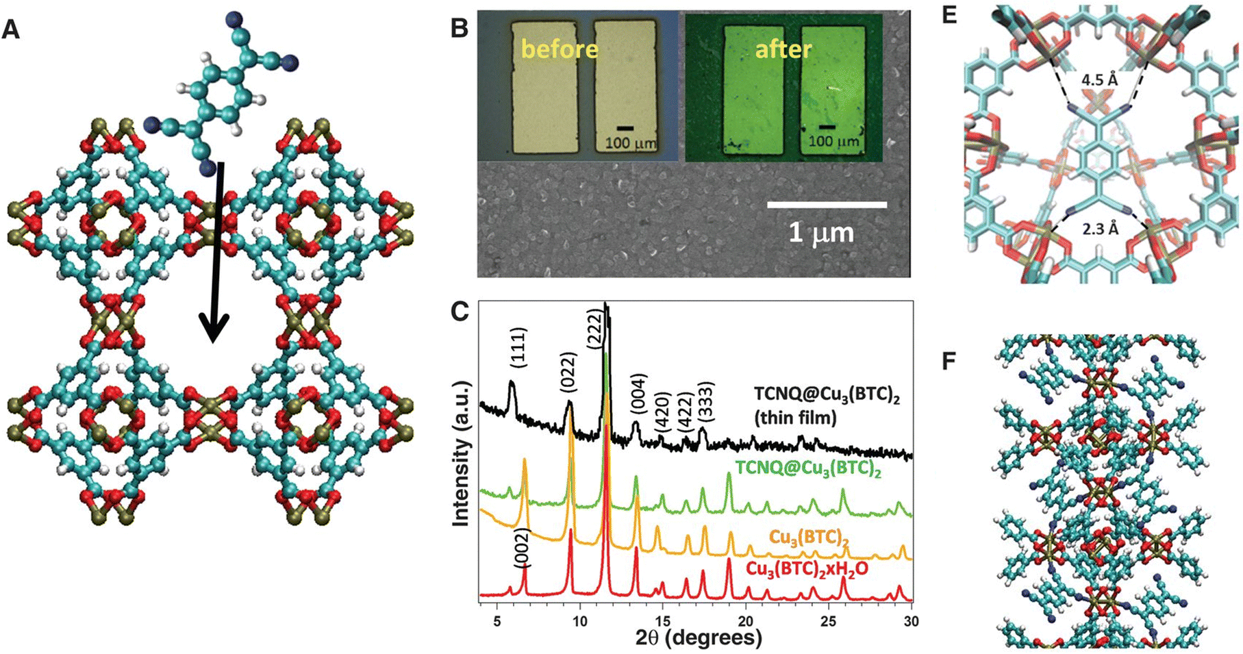 | ||
| Fig. 12 Fabrication of conductive MOF thin-film devices and structural characterization. (a) TCNQ molecule shown above a Cu3(BTC)2 MOF; arrow points into the pore. Colour code: H = white, N = blue, C = cyan, O = red and Cu = light brown. (b) SEM image of a MOF-coated device; insets are optical images of devices before and after TCNQ infiltration. (c) XRD data for powder and grazing incidence XRD for a thin film. (e) Minimum-energy configuration for TCNQ@Cu3(BTC)2 obtained from ab initio calculations. (f) Possible configuration that would provide a conductive channel through the MOF unit cell. Reproduced with permission from ref. 89. Copyright 2014, The American Association for the Advancement of Science. | ||
The presence of metal–ligand coordination-mediated charge transfer interaction increases the conductivity by about six orders of magnitude. HKUST is a poorly conducting MOF having a conductivity of 10−8 S cm−1 at room temperature while the electrical conductivity of TCNQ@HKUST-1 reached a value of 7 × 10⁻² S cm−1 with an activation energy of 41 meV. Ab initio calculations indicate that TCNQ guest molecules cross linked the dimeric Cu paddlewheels within the MOF leading to strong electronic coupling between the dimeric Cu subunits.
Through-bond charge transport might be the cause of the increase in the conductivity of TCNQ@HKUST-1 (Fig. 13). This charge transport was confirmed by substituting TCNQ with its saturated analogue H4TCNQ. H4TCNQ@HKUST-1 shows a similar conductivity to HKUST-1 itself. This H4TCNQ was unable to delocalize the carriers (Fig. 13). Later, Allendorf, Fischer and co-workers synthesized TCNQ incorporated HKUST-1 with the precise molecular formula TCNQ1.0@Cu3BTC2 that shows an electrical conductivity value of 1.5 × 10⁻⁴ S cm−1. They have also tried to provide insight on the location and binding of TCNQ within the MOF.109 Thürmer et al. have encapsulated TCNQ within pre-deposited thin films of HKUST-1 on ITO. These TCNQ loaded HKUST-1 thin films show 1010 times higher electrical conductivity (10−1 S cm−1) than the parent MOF (10−11 S cm−1).110 A similar study performed by Deep et al. showed that encapsulated TCNQ within the thin film of HKUST-1 on a gold-screen printed electrode has 109 times more conductivity than the host MOF.111 In a third related study, Jung and co-workers showed a 107 times enhancement of the electrical conductivity (2.42 × 10⁻⁴ S cm−1) through impregnation of TCNQ within thin films of HKSUT-1 obtained by solution shearing process.112
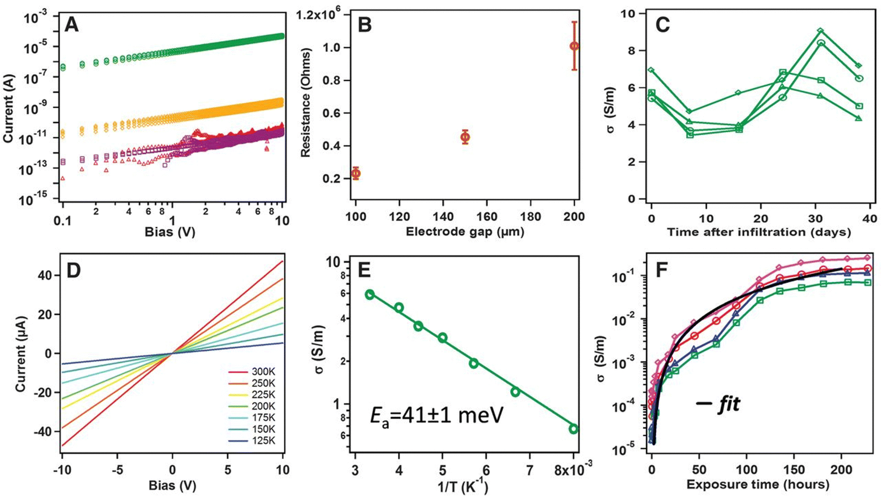 | ||
| Fig. 13 Electronic transport characteristics of MOF thin film devices. (a) I–V curves before (red) and after insertion of TCNQ (green), F4-TCNQ (gold), or H4-TCNQ (purple). (b) Channel-length dependence of conductivity for TCNQ-infiltrated devices; error bars denote standard deviations. (c) Stability of conductivity over time for several devices. (d) I–V curve temperature dependence. (e) Arrhenius plot of the conductivity. (f) Conductivity versus exposure time for several devices. The black line is a fit to percolation theory, σ = 4 × 10⁻⁶ (t − 0.5)2, where t is exposure time. Reproduced with permission from ref. 82. Copyright 2014, The American Association for the Advancement of Science. | ||
Vittal, Loh and co-workers have developed a conductive thin film of a MOF with inserted TCNQ. By changing the reaction conditions from simple mixing to slow solvent diffusion, they have synthesized nano-sheets of the 2D MOF [Cu2(AcO)4(CuTPyP)1/2]·CHCl3 (H2TPyP = 5,10,15,20-tetra-4-pyridyl-21H,23H-porphine) and transfer them to the substrate. The atomic force microscopy (AFM) study indicates the average thickness of the nano-sheets is about 70 nm. For electrical conductivity measurements, they also prepared thin films of the 2D MOF on silicon wafers and then TCNQ was incorporated within the thin films. The resultant TCNQ@2D-MOF shows 103 times higher conductivity than the parent MOF (10−9 S cm−1). They have demonstrated that the charge transfer interaction between the host and TCNQ guest molecules is the main reason behind such an increment in the electrical conductivity.90
Recently, Shiozawa et al. have prepared thin films of TCNQ@Co-MOF-74 on glass substrates following the previous results. They observed that thin films of TCNQ@Co-MOF-74 are more conductive than the parent Co-MOF-74 (insulating in nature), although they are less conductors than TCNQ@HKUST-1 since TCNQ cannot build a conductive pathway within the honeycomb structure of Co-MOF-74 in contrast to HKUST-1.113
TCNQ has also been incorporated within the voids of the 3D MOF [Cu2(TATAB)3]·7.5H2O (where H3TATAB = 4,4′,4′′-((1,3,5-triazine-2,4,6-triyl)tris(azanediyl))tribenzoic acid) by Xu et al.114 The TCNQ@MOF has 104 times higher conductivity than the parent MOF. These authors have demonstrated that the insertion of the unoccupied molecular orbitals of TCNQ molecules into the HOMO–LUMO gap of the MOF formed a charge transport channel within the 3D MOF, facilitating the conduction of electrons.114
A significant enhancement of the electrical conductivity has been recently reported by Sindhu and Ballav by depositing HKUST-1 on TCNQ-doped HKUST-1.115 Pure MOF HKUST-1 thin film shows an electrical conductivity of 10−8 S cm−1 and the encapsulation of TCNQ increases the conductivity to 10−3 S cm−1. The deposition of HKUST-1 on TCNQ@HKUST-1 shows a further enhancement of the conductivity.115
Zeng et al. have shown the possibility of tuning the electrical conductivity of [Zn3(DL-lac)2(pybz)2]·2.5DMF (where DL-lac = lactate and pybz = 4-pyridine benzoate) through I2 loading within the 1D channels (∼11 × 10 Å) by soaking the MOF in a cyclohexane solution of I2 (Fig. 14). The electrical conductivity of I2@MOF is 3.42 × 10⁻³ S cm−1 along the channels and 1.65 × 10⁻⁴ S cm−1 in the direction perpendicular to the channels. Both values are much higher than those of the pristine MOF (7 × 10⁻⁶ S cm−1). The authors demonstrated that the donor–acceptor interaction between the loaded I2 and the aromatic pore walls is the reason for conductivity enhancement.117 They have also tuned both the electrical and magnetic properties through the incorporation of I2 within the channels of [CoII3(lac)2(pybz)2]·3DMF (where pybz = 4-pyridyl benzoate and lac = D- and L-lactate). Iodine incorporation has been done by soaking single crystals of the desolvated framework within a saturated solution of I2 in DMSO/H2O (v/v = 1:1) or in cyclohexane. The DMSO:water solution leads to the partially oxidized framework [CoIIICoII2(pybz)2(lac)2(H2O)2](I−)·2H2O·1.5DMSO, which is ferromagnetic, in contrast to the antiferromagnetic parent MOF. In contrast, when the insertion is performed in cyclohexane, the crystals form a framework with the formula {[CoII3(pybz)2(lac)2]·2.7I2} and a conductivity of 7 × 10⁻⁶ S cm−1.118
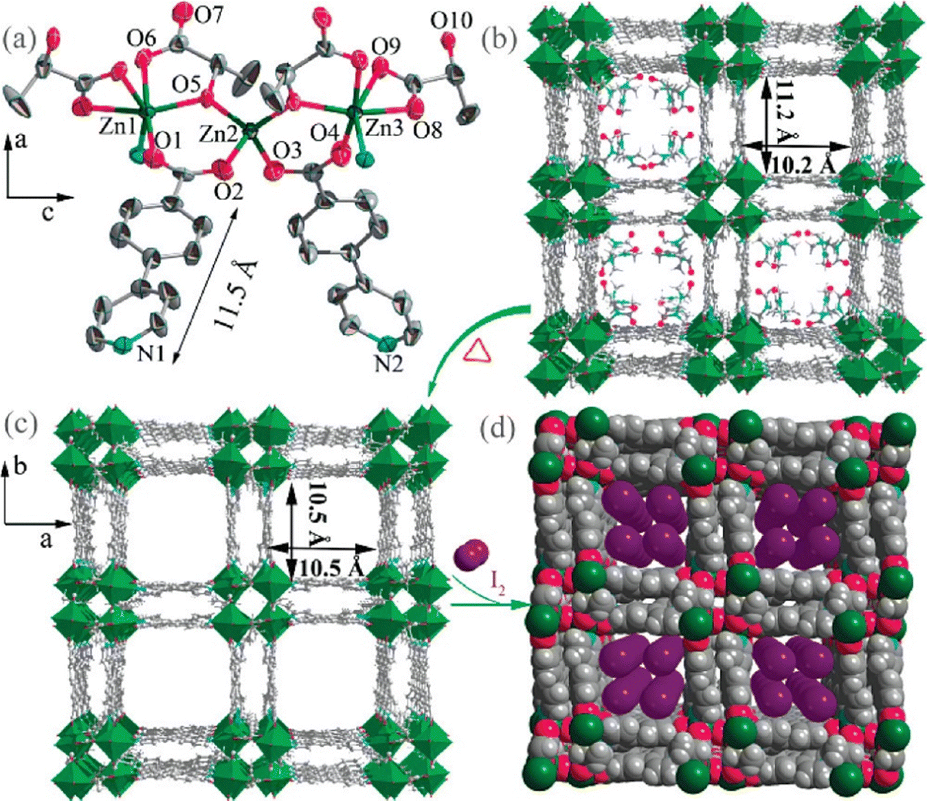 | ||
| Fig. 14 (a) Coordination environment of Zn atoms in [Zn3(DL-lac)2(pybz)2]·2.5DMF (H-atoms are omitted for clarity). (b) Perspective views of the 3D open framework with 1D channels in [Zn3(DL-lac)2(pybz)2]·2.5DMF with the guest DMF molecules. General colour code: Zn, green; N, blue; O, red; C, gray. (c) The completely desolvated framework of [Zn3(DL-lac)2(pybz)2]·2.5DMF, showing the empty channels. (d) Location of the I2 molecules in the channels of the desolvated framework of [Zn3(DL-lac)2(pybz)2]·2.5DMF. The PLATON calculated void space in the desolvated framework of [Zn3(DL-lac)2(pybz)2]·2.5DMF is 43.8%. Reproduced with permission from ref. 117. Copyright 2010, The American Chemical Society. | ||
Kobayashi et al. have developed a redox-active dithiolate-based MOF Cu[Ni(pdt)2] (CuNi) (pdt2− = pyrazine-2,3-dithiolate), which is isostructural to Cu[Cu(pdt)2] (CuCu). In contrast to CuCu, whose framework collapses upon desolvation, CuNi retains its structure upon desolvation, allowing the incorporation of I2 vapour within the channels of the framework. The resultant I2@CuNi shows 104 times higher conductivity (10−4 S cm−1 with an activation energy of 490 meV) than the parent CuNi MOF (10−8 S cm−1). This might be due to the partial oxidation of the [NiII(pdt)2] centres that results in an increase in the charge carriers responsible for the improved conductivity.119
The I2 doped MOF [Cu6(pybz)8(OH)2]·(I5)·(I7) has been synthesized using the in situ template method by Yin et al.120 Structural studies show that the resulting framework contains I5− and I7− polyiodides within the channels anchored by weak interactions between the polyiodides and the aromatic pore-walls (Fig. 15). Keeping the compound in dry methanol leads to the removal of the polyiodides, leading to the I−-containing framework [Cu6(pybz)8(OH)2](I)2·3.5CH3OH. The polyiodide-encapsulated MOF shows 102 times higher electrical conductivity (8.11 × 10⁻⁷ S cm−1) than the iodide: I-@MOF (8.04 × 10⁻⁹ S cm−1). These data indicate that the conductivity decreases with decreasing the amount of iodide in the channels. The non-covalent interactions between the polyiodides and the aromatic walls of the MOF provide the charge transport pathway.120
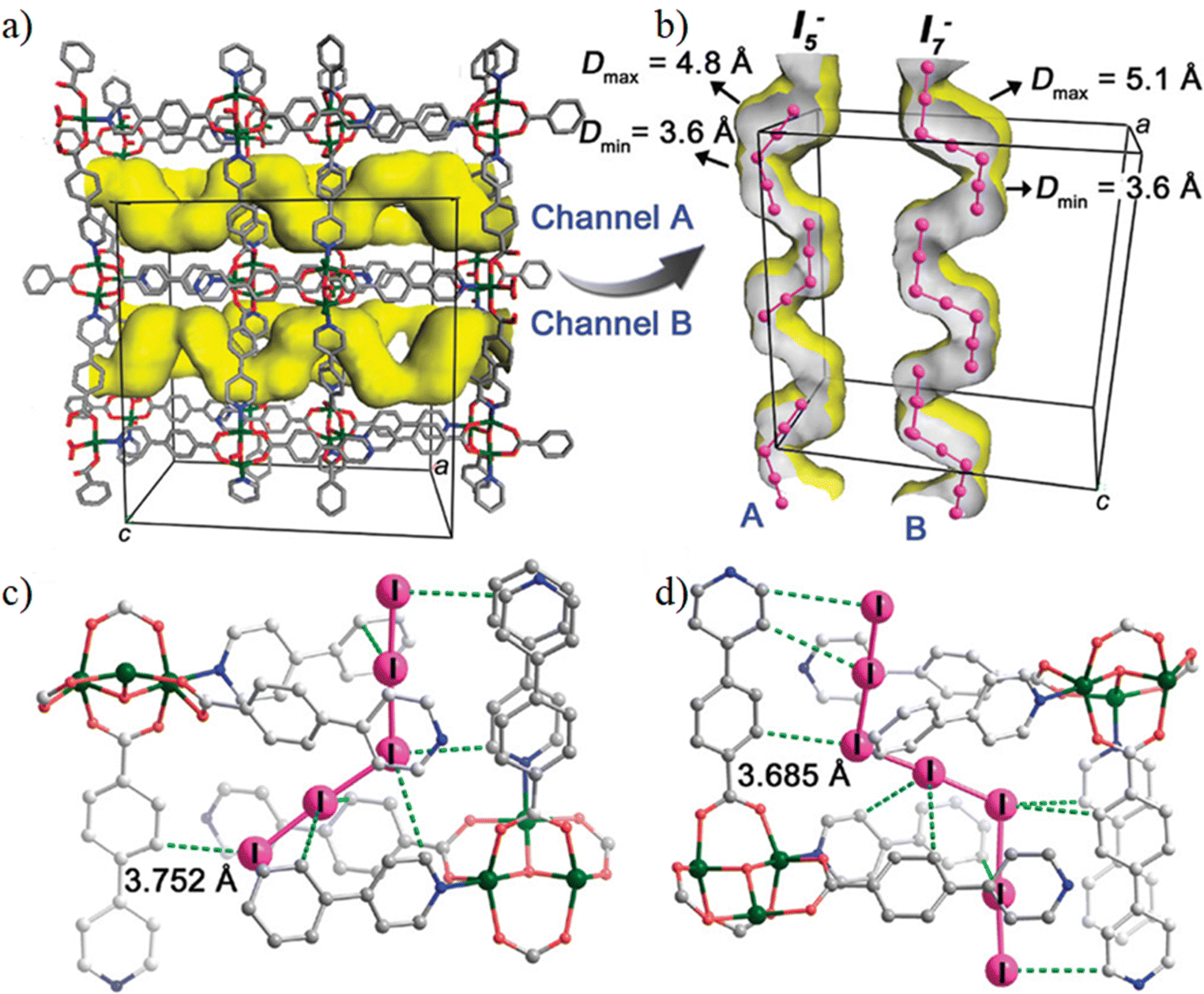 | ||
| Fig. 15 (a) Perspective view of the S-shaped channels along the a-axis in [Cu6(pybz)8(OH)2]·(I5)·(I7). (b) Section drawing of the A and B channels in each cell lattice. (c) The environment of I5− in channel A; the distances from I atoms to C atoms of phenyl or pyridyl rings are in the range 3.732–3.999 Å. (d) The environment of I7− in channel B; the distances from I atoms to C atoms of phenyl or pyridyl rings are in the range of 3.685–4.281 Å. Reproduced with permission from ref. 120. Copyright 2012, The American Chemical Society. | ||
Iodine has also been incorporated by Han and co-workers within the thin films of two different Co-MOFs: [Co-NDC] and [Co-BDC], by using two different ligands (NDC = 2,6-napthalenedicarboxylic acid and BDC = 1,4-benzene dicarboxylic acid).121 Layer-by-layer thin films of the MOFs were prepared on TiO2 films and iodine incorporation was done by dipping the thin films in a saturated acetonitrile solution of I2. Both parent MOFs are insulating and iodine incorporation increases both the carrier concentration (+1.14 × 10¹¹ and +5.48 × 1011 cm−3) and mobility (21.2 and 87.6 cm2 V−1 s−1) for both MOF thin-films, respectively. The insulating [Co-NDC] MOF becomes semiconducting with a conductivity value of 1.88 × 10⁻⁶ S cm−1.121 In this case, the enhancement of the conductivity is due to ligand oxidation by I2 that was confirmed by XPS analysis and by absorption spectroscopy.122
The crystal structure of the iodine encapsulated MOF [Co3(BDC)3(H2bpz)2]·2DMF·8H2O (H2BDC = 1,4-benzenedicarboxylic acid, H2bpz = 3,3′,5,5′-tetra methyl-4,4′-bipyrazole) has been established by Li et al. after post-synthetic iodine loading.123 The parent MOF undergoes a single crystal to single crystal (SCSC) transformation to form the I2-containing MOF [Co3(BDC)3(H2bpz)2]·I2·2DMF. The I2 molecules interact with the host framework through C–H⋯I hydrogen bonding interactions. I2@MOF shows 103 times higher conductivity (1.56 × 10⁻⁸ S cm−1) than the parent MOF (2.5 × 10⁻¹¹ S cm−1). The authors propose that the n–σ* host–guest charge transfer is the main reason for conductivity enhancement.123
Hu et al. have measured the electrical conductivity of the MOF [Tb(Cu4I4)(ina)3(DMF)] (ina = isonicotinate) that has two different types of channels (A and B), upon iodine uptake and release. I2 uptake is carried out by soaking the parent MOF in a saturated I2 cyclohexane solution for 2 hours while I2 can be released by heating the I2@MOF. The parent MOF has a conductivity of 5.72 × 10⁻¹¹ S cm−1 that increases by a factor of 107 to a value of 2.16 × 10⁻⁴ S cm−1 after I2 uptake. The release of I2 again decreases the conductivity to 10−10 S cm−1. A structural study of the I2-loaded MOF shows that channel A contains half an I2 molecule per formula unit whereas channel B contains one I2 molecule. In channel A, the I2 molecules interact with the aromatic ligands and with the iodides of the Cu4I4 moieties to form I−⋯I2⋯I− polyiodide chains. On the other hand, the I2 molecules of channel B interact with the aromatic pore walls only. So, the interaction of [Cu4I4] with the guest I2 molecules forms [Cu4I5]n layers, which is the conducting pathway for the MOF.124
The important role of iodine on the conductivity of MOFs was further confirmed by Schröder and co-workers125 on two different MOFs, [VIII2(OH)2(L)] and [VIV2(O)2(L)] (H4L = biphenyl-3,3′,5,5′-tetracarboxylic acid), where iodine was incorporated by iodine vapour diffusion after desolvation of the MOF. The crystal structures of the I2@MOFs were determined by high-resolution synchrotron powder X-ray diffraction. Structural analysis of I2@[V2(OH)2(L)] shows the presence of three I2 molecules and one I3− ion within the channels. The formation of I3− implies the oxidation of VIII centres. BVS calculation shows that the overall valence is 3.28 for the V centre and the complex is denoted by I2@[VIIIVIV(OH)2(L)]. The I3− ions are located close to the –OH groups, and there is a strong hydrogen bond between the I3− and –OH groups, although the H atom cannot be located from the XRPD data. The I2 molecules are located near the phenyl rings and are stabilized by intermolecular interactions. In [VIV2(O)2(L)], the incorporation of I2 does not lead to oxidation of the framework and the I2 molecules interact with each other to form helical chains within the channels of the MOF to form an overall complex formulated as I2@[VIV2(O)2(L)]. Electrical conductivity measurements show that the conductivity increases 107 times for [VIII2(OH)2(L)] upon iodine incorporation while it remains almost the same for [VIV2(O)2(L)]. These data indicate that the host–guest charge transfer interaction enhances the electrical conductivity of the material.125
Ballav et al. have reported the enhancement of the electrical conductivity of SURMOF (surface-mounted metal–organic framework) thin films of Cu-TCNQ through iodine incorporation. Mercaptoundecanoic acid (MUDA), bearing polar –COOH and –SH head-groups linked together via a –(CH2)10– moiety, was used to form self-assembled monolayers (SAMs) on semiconducting FTO coated on glass and metallic gold. Cu-TCNQ SURMOF thin films were deposited by sinking the SAMs in the solution of copper acetate in EtOH and TCNQ in EtOH. I2 was incorporated within the channels of the MOF by using iodine vapour. Electrical conductivity measurements show that the iodine-incorporated SURMOF shows 100 times higher conductivity (10−3 S cm−1) than the parent MOF itself (10−5 S cm−1). In the parent SURMOF, copper is present in its +1 oxidation state while the TCNQ is present as a TCNQ radical anion as suggested by the Raman spectroscopy and EPR studies. The coordination of the TCNQ radical anion with Cu+ within the parent SURMOF is the reason behind its high conductivity, although a certain amount of the TCNQ radical anion undergoes disproportionation into the TCNQ molecule and the TCNQ dianion. I2 oxidizes the TCNQ radical anion to the neutral TCNQ molecule with consequent formation of the I3− ion but Cu+ remains unaltered. So, this charge transfer is only ligand oriented and this is the main reason for the enhancement of conductivity.126
In a similar manner, the enhancement of the electrical conductivity of the MOF [Eu4(BPT)4(DMF)2(H2O)8] (where H3BPT = biphenyl-3,4′,5-tricarboxylate) through incorporation of iodine was studied by Zhang et al. They have observed that the electrical conductivity of the I2-doped MOF increases with increasing temperature from 25 to 80 °C under anhydrous conditions. Although the MOF loses some amount of doped I2 on heating, the conductivity increases from 8.27 × 10⁻⁷ S cm−1 to 2.71 × 10⁻⁵ S cm−1. Polyiodide ions, formed within the channels of the MOF, promote the n to σ* transition with high efficiency and this is the reason for the observed conductivity enhancement.127
In some cases, the loading of iodine enhances the electrical conductivity of the host MOF only marginally. D’Alessandro and co-workers have reported the enhancement of the electrical conductivity of [Zn2(TTFTB)(H2O)2] (where TTFTB = tetrathiafulvalene tetrabenzoate) through iodine loading by using iodine vapour. Iodine oxidizes the ligand to TTFTB˙+ with formation of iodide and polyiodides. Such a host–guest charge transfer phenomenon increases the electrical conductivity of the parent MOF from 2.5 × 10⁻¹⁰ S cm−1 to 1.6 × 10⁻⁹ S cm−1.128
In another example, Zuo et al. have reported a small improvement in the electrical conductivity of lanthanoid-tetrathiafulvalene-based MOFs through incorporation of iodine within the MOFs. Iodine oxidizes the ligand tetrathiofulvalene (TTF) to TTF˙+ but the weak enhancement of the conductivity is due to a lack of band formation.129 In another article, the same group has reported the enhancement in the electrical conductivity of two different 3D MOFs [Fe(dca)2]2[TTF(py)4]·CH2Cl2 and [Fe(dca)][TTF(py)4]·ClO4·CH2Cl2·2CH3OH having the redox active ligand tetra(4-pyridyl)tetrathiafulvalene (TTF-(py)4) and spin-crossover FeII centres (dca = dicyanamide). Iodine loading was done by immersing the crystals of the complexes in an I2 saturated solution in cyclohexane. Single crystal X-ray structural studies of the I2@MOFs indicate the formation of TTF˙+ radical cations with consequent reduction of iodine to I3− which is also confirmed by XPS and EPR studies. Electrical conductivity measurement shows a 103 times increment of conductivity for both cases.130
Gordillo et al. have developed a semiconducting MOF [Zn3(ExTTFTB)2(H2O)4·6EtOH] (where ExTTFTB is an electron-rich π-extended tetrathiafulvalene ligand equipped with four benzoic acid units). The ExTTFTB ligand has a butterfly-like shape and is decorated with four benzoic acid units and forms a porous 3D double-helical MOF by reacting with Zn(NO3)2. Structural analysis shows that the ExTTFTB ligand is highly constrained with unsymmetrical electron distribution due to the different binding modes of the four carboxylate groups. These distortions critically change the redox behaviour of the ligand. The free ligand shows one two-electron oxidation step to form the planar ExTTFTB2+ dication, while the ligand within the MOF undergoes a one-electron oxidation to form the radical cation ExTTFTB˙+. Iodine was incorporated within the pores of the MOF by placing it in iodine vapour. Electrical conductivity measurement shows that I2@MOF has 104 times higher conductivity (10−6 S cm−1) than the parent MOF (10−10 S cm−1). EPR studies show that a large amount of ExTTFTB ligand was oxidized to form ExTTFTB˙+ radical cation upon I2 loading. The charge transfer interaction between ExTTFTB˙+ and ExTTFTB forms donor–acceptor chains which act as the charge transport pathway.131 In another article, the same group demonstrated a 100 times enhancement of the electrical conductivity of the Tb-containing parent MOF (Tb-ExTTFTB) with the same ligand, upon I2 loading.132 Similarly, Valente et al. have reported a 103 times enhancement of the electrical conductivity of a perylene-based MOF through encapsulation of iodine. The perylene-based MOF shows weak electron conduction (10−8 S cm−1) while the encapsulation of iodine leads to the formation of I3− with consequent oxidation of perylene. Two-probe electrical conductivity measurements on single crystals of the host–guest show an enhanced electrical conductivity value of ∼10−5 S cm−1.133
One of us has performed extensive research on the incorporation of TTF within the channels of MOFs/PCPs to design conductive materials. In 2000, Coronado, Gómez-García et al. showed the presence of magnetoresistance in a host–guest system formed by the in situ encapsulation of BEDT-TTF within the interlamellar space of a 2D magnetically ordered framework. The host–guest (BEDT-TTF)3[MnCr(C2O4)3] (C2O42− = oxalate dianion) was synthesized by electro-crystallization using tris(oxalate)chromate(III) and MnII salt in a 2:3 ratio in the presence of BEDT-TTF. Structural analysis shows that BEDT-TTF cations form pure pseudohexagonal β-type supramolecular layers within the honeycomb 2D coordination layers of [MnCr(C2O4)3]−. The accumulated charge per BEDT-TTF moiety is +1/3. The material shows magnetic long-range order below 5.5 K with the presence of magnetic hysteresis at 2 K. In plane, four-probe electrical conductivity measurements show the largest room temperature conductivity found in a conductive ec-MOF (∼250 S cm−1). Furthermore, this compound shows a metallic conductivity within the temperature range of 2–300 K.137 Application of a magnetic field perpendicular to the layers shows the presence of negative magnetoresistance below 10 K. The same authors reported a similar host–guest framework with the Selenium-substituted organic donor bis(ethylenedithio)-tetraselanafulvalene (BEDT-TSF): (BEDT-TSF)3[MnCr(C2O4)3] (Fig. 16).138 As observed in the previous structure, the (BEDT-TSF) moieties are located within the interlamellar space of the 2D honeycomb layers of [MnCr(C2O4)3]−, and similarly, the average charge on each (BEDT-TSF) moiety is +1/3. The magnetic framework also shows a high room temperature electrical conductivity of 1 S cm−1 and a metallic conductivity within the range of 150–300 K. The difference in conductivity is due to the effective distance between the donor moieties.
 | ||
| Fig. 16 Representation of the structure of [BETS]x[MnCr(ox)3]·(CH2Cl2): idealized side view of the alternating layers (up) and top view of the organic layer (down). Reproduced with permission from ref. 138. Copyright 2003, The American Chemical Society. | ||
The same group also prepared the host–guest charge transfer complex formulated as (BEDT-TTF)x[MnRh(C2O4)3]·CH2Cl2 (where x = 2.526(1)) by replacing Cr with Rh. The room-temperature electrical conductivity of this compound is 13 S cm−1 and shows a metallic behaviour, reaching a very high value of 28 S cm−1 at 103 K. The difference in the conductivity value was attributed to small structural differences.139 The use of other trivalent and divalent metal ions and other TTF-type organic donors gave rise to more than a dozen examples of compounds with magnetic ordering and high electrical conductivities in the range of 0.1–21 S cm−1, which were reported in a series of articles published by Coronado, Gómez-García et al.140–143
Later Zhang and co-workers encapsulated BEDT-TTF within the interlamellar space of homometallic 2D coordination polymers. An electro-crystallization method was employed to synthesize the framework (BEDT-TTF)3[Cu2(C2O4)3]·3H2O. Structural analysis shows that each asymmetric unit contains three BEDT-TTF moieties, and they are stacked face-to-face to form 1D stacks along the a-axis. These columns are further packed through S⋯S interactions to form 2D supramolecular layers known as θ21-phase.144 The donor 2D supramolecular layers are located between the anionic honey-comb coordination layers of [Cu2(C2O4)3]2−. The average formal average charge on each BEDT-TTF molecule is +2/3, although there is an inhomogeneous charge distribution, as confirmed by Raman spectra. Four-probe electrical conductivity measurements show a high room temperature conductivity of ∼4 S cm−1, although it shows a semiconducting behaviour and becomes insulating at low temperatures, due to an inhomogeneous charge distribution.145
The same authors prepared another charge transfer complex by incorporating the Se-containing donor BEDT-TSF within the interlayer space of the same 2D homometallic anionic coordination layers using a similar electro-crystallization method. Similarly, each asymmetric unit contains three BEDT-TSF moieties and they form 2D donor layers through S⋯S, S⋯Se and Se⋯Se interactions. The average formal charge is also +2/3, as confirmed by Raman and EPR spectral analyses. Four probe electrical conductivity measurements show a very high room temperature conductivity of 140 S cm−1 and a metallic behaviour from 300 K to 180 K. The conductivity remains approximately constant within the temperature range of 180 to 150 K and below 150 K decreases to a value of 10 S cm−1 at 17 K to become insulating below 12 K. The large difference in conductivity value of the BEDT-TTF and BEDT-TSF based structures is due to the larger size and diffused electron density of Se compared to S. Theoretical analysis reveals that overlap integral for BEDT-TSF based structure is twice that of the BEDT-TTF containing material and band dispersion is stronger for the Se-containing compound.146
Using a solvothermal synthetic method, Saha et al. have very recently prepared another conducting framework by encapsulating TTF within the interlamellar spaces of a 2D framework.147 Thus, a structure similar to MOF-74, could be prepared by the reaction of the electron acceptor DSNDI (DSNDI = 4,4′-(1,3,6,8-tetraoxobenzo[lmn][3,8]phenanthroline-2,7(1H,3H,6H,8H)-diyl)bis(2-hydroxy benzoic acid), prepared by reaction between naphthalene dianhydride (NDA) with 4-aminosalicylic acid with zinc salts at 90 °C). The framework contains large hexagonal channels with an average pore size of ∼3.1 nm. The optical bandgap of the host MOF is calculated to be 2.1 eV. The TTF loading was done by soaking the activated material in a TTF solution for 2 days, and the loading was identified by the colour change to brownish. The optical bandgap of the TTF@MOF becomes ∼1 eV. The formation of charge transfer between TTF and MOF was confirmed by the appearance of a new band at 900 nm, and this was also further confirmed by EPR spectroscopy. Such a decrease in the bandgap is due to the intercalation of TTF moieties between electron-deficient DSNDI ligands.147
Corma et al. showed that the intercalation of TTF in the delaminated 2D zeolite framework ITQ-2 generates stable TTF+ radicals within the open cups of the external surface, as demonstrated by EPR measurements.148
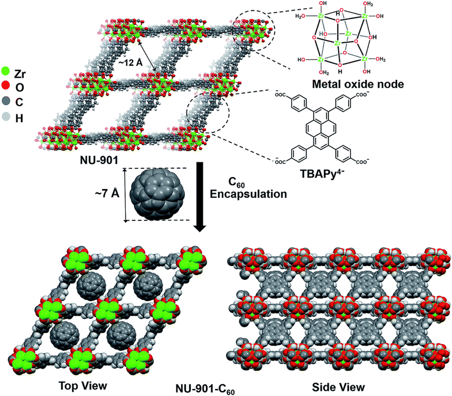 | ||
| Fig. 17 Immobilization of C60 within the rhombus-shaped channels of NU-901. The chemical structures of the individual components of NU-901 are shown. The diameter of C60 (7 Å) is well suited for encapsulation in NU-901 with a pore aperture of 12 Å. The top and side views of the composite NU-901-C60 are shown. The top and side views are DFT-optimized structures in the limit of full occupancy of the diamond pores by the fullerene guest, i.e., 1:1 occupancy. Reproduced with permission from ref. 91. Copyright 2018, The Royal Society of Chemistry. | ||
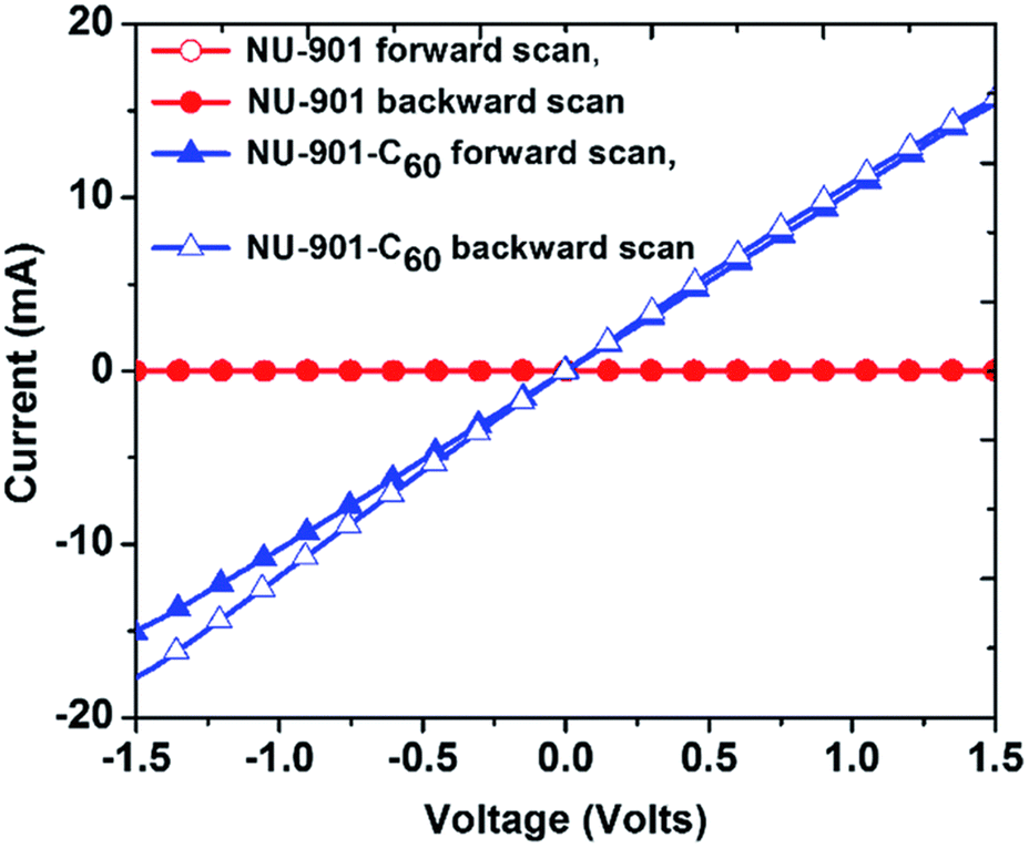 | ||
| Fig. 18 I–V plot for pressed pellets of NU-901 and C60@NU-901. The scan was performed from −2 V to 2 V, and the scan rate was 50 mV s−1. Reproduced with permission from ref. 91. Copyright 2018, The Royal Society of Chemistry. | ||
The authors of this study proposed that the charge transfer interaction between the fullerene and the ligand (TBAPy)4− of the framework is responsible for the enhancement of the electrical conductivity. In order to further strengthen it, they also used the electron-rich tetra-amino(phenyl-substituted) based ligand replacing the original TBAPy4− ligand. The synthesized NU-901-amino MOF has a similar structure than the original (TBAPy)4−-containing MOF. Intercalation of fullerene in this new MOF NU-901-amino results in a higher conductivity than that observed in C60@NU-901 due to enhanced charge transfer interaction between fullerene and the ligand in NU-901-amino. DFT calculations also show that for the host frameworks, both the valence band maxima and conduction band minima contain contributions from the π-orbitals of the ligand while upon encapsulation of fullerene, the minima of the conduction band is predominantly composed of fullerene molecules. Additionally, the fullerene encapsulation reduces the band gap by 1.2 eV in both cases. Ray and co-workers have shown, theoretically, that the incorporation of hetero-fullerenes within the void space of MOFs may have more impact on the electrical conductivity of MOFs than fullerenes.150
A significant conductivity enhancement through encapsulation of C60 within a mesoporous tetrathiafulvalene (TTF)-based MOF: [(TTFTB)3[(Fe3O)(H2O)2(OH)]2] (where H4TTFTB = tetrathiafulvalene tetrabenzoic acid) was reported by Mínguez and co-workers.151 Fullerene loading was done by soaking the activated MOF within an o-dichlorobenzene solution of fullerene for 3 days at 60 °C. C60@MOF shows a 100 times higher conductivity (4.7 × 10⁻⁹ S cm−1) than the parent MOF (3.7 × 10⁻¹¹ S cm−1). The authors proposed that the donor–acceptor charge transfer interaction between the C60 molecules and TTF-based linkers is the reason behind the enhancement of the electrical conductivity.151
Liu et al. incorporated C60 into two different porous MOFs: [Zn(TPP)] and [Cu(BPDC)] (where TPP = 5,15-bis-(3,4,5-trimethoxyphenyl)-10,20-bis-(4-carboxyphenyl) porphyrinato and BPDC = 4,4′-biphenyl-dicarboxylate). Fullerene-encapsulated MOFs show higher electrical conductivity than the unloaded frameworks. Thus, C60@Zn(TPP) and C60@Cu(BPDC) show conductivities two and four orders of magnitude higher than their parent structures, respectively. This difference is obviously due to different host–guest charge transfer interactions based on the ligand architecture and pore dimensions. Nevertheless, the photo-conducting response of C60@Zn(TPP) is much better than that of C60@Cu(BPDC).152
In 1997, Coronado, Gómez-García et al. prepared a series of layered magnets with the decamethylferrocenium cation (FeCp*2)+ inserted into the interlayer space of oxalate-based 2D honeycomb heterometallic magnets of the type [MIIMIII(C2O4)3]− with MII = Mn, Fe, Co, Cr, Ni and Cu and MIII = Cr and Fe.155 The same authors extended the initial work with decamethyl–cobaltocenium (CoCp*2)+ and decamethyl–manganocenium (MnCp*2)+ with different MII and MIII ions, including solid solutions of CrIII and FeIII in different proportions.156–162
In 2006, Fischer et al. successfully synthesized a Fc-containing MOF where the guest Fc molecules are interpenetrated within the host framework through van der Waals interactions without altering the structure.163 Later, Fischer and co-workers incorporated Fc within the structure of MIL-53(Al) by grafting 1,1′-ferrocenediyl-dimethylsilane.164 Heck et al. have studied the ferrocene loading within the pores of two different MOFs: [Cu2(BDC)2(dabco)] and [Cu2(ndc)2(dabco)] (where H2BDC = 1,4-benzene dicarboxylic acid, ndc = 1,4-naphthalene-dicarboxylate and dabco = 1,4-diazabicyclo-[2.2.2]-octane) by exposing the MOFs to ferrocene vapour. Mössbauer spectroscopic studies indicate that the redox behaviour does not alter after ferrocene loading.165
Ferrocene incorporation was also performed by Dragässer et al. to enhance the electrical conductivity of thin films of HKUST-1 MOF (Fig. 19 and 20). Self-assembled monolayers (SAM) of mercaptohexadecanoic acid were prepared on a gold electrode over Si, and thin films of HKUST-1 were prepared by sinking the SAM in solutions of copper(II) acetate and trimesic acid, respectively. Ferrocene loading was done by exposing the thin films in ferrocene vapour. Electrical conductivity measurement shows that the ferrocene@MOF has a conductivity of 2 × 10⁻⁹ S cm−1, 50000 times higher than that of ferrocene (10−14 S cm−1). Within the pores of HKUST-1, ferrocene undergoes oxidation to ferrocenium (Fc)+ and such charge transfer is the prime reason behind the increment of conductivity.166 In another article, the same group developed a tunnelling junction by depositing a Hg droplet with passivated hexadecanethiol and observed that the Fc@MOF shows 2.5 times higher conductivity than the parent HKUST-1 MOF (Fig. 19).167
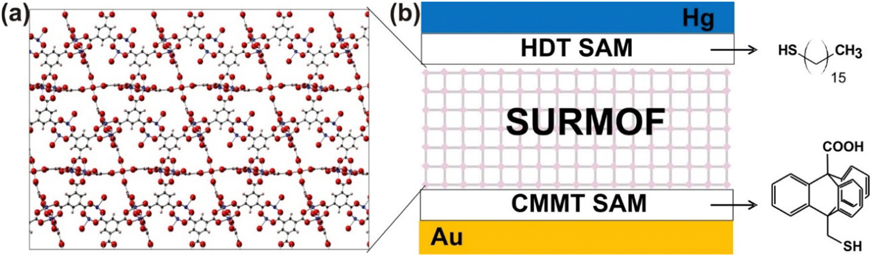 | ||
| Fig. 19 Scheme of the Hg-based tunnelling junction. (a) Crystal structure of HKUST-1 with [111] orientation with respect to the Au surface. O, C and Cu atoms are coded in red, blue, and black colours, respectively. (b) Contact area between the two electrodes: Hg as the top electrode is passivated with a SAM made of hexadecanethiol (C16H33-SH, HDT), whereas the SURMOF grown on a 9-carboxy-10-(mercaptomethyl) triptycene (CMMT) modified Au substrate serves as the bottom electrode. The molecular formulas of HDT and CMMT are presented on the right side. Reproduced with permission from ref. 166. Copyright 2012, The Royal Society of Chemistry. | ||
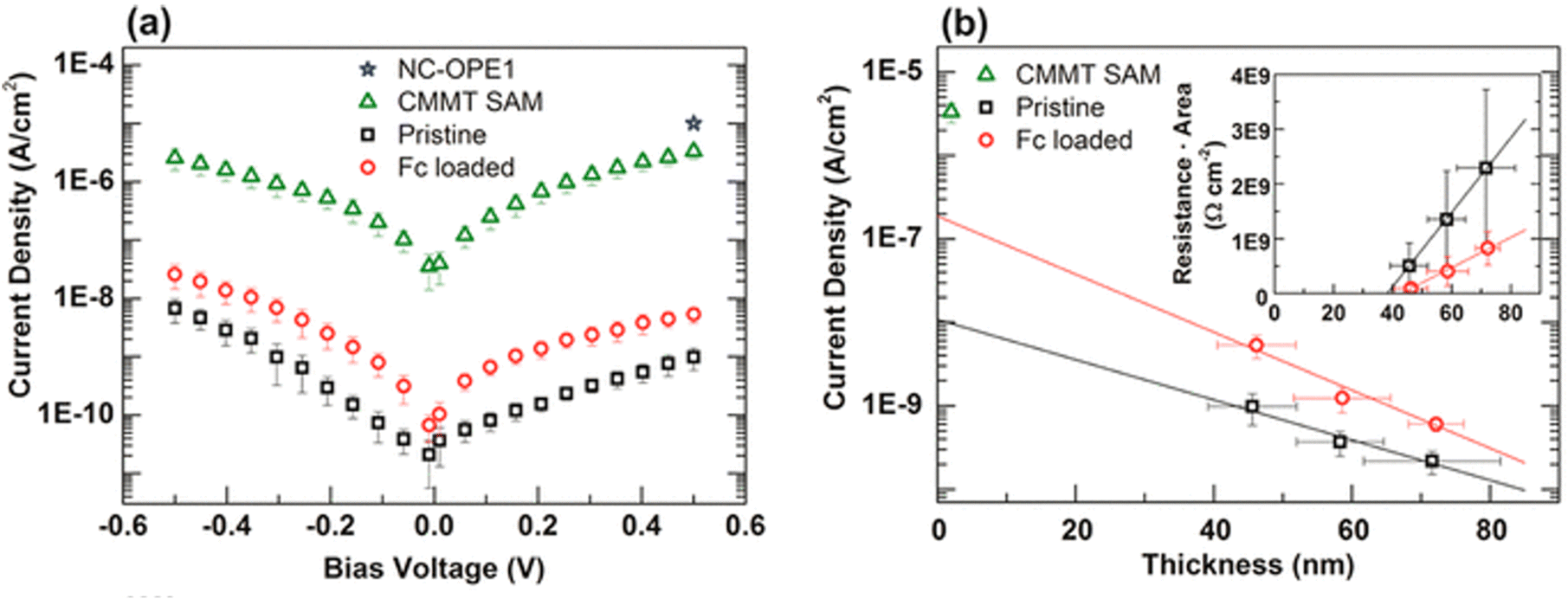 | ||
| Fig. 20 (a) Current density (logarithmic scale) vs. V plot for HKUST-1 SURMOF, prepared by 5 spraying cycles, before (black empty squares) and after (red empty circles) ferrocene loading. Green empty triangles correspond to the CMMT SAM. The blue star represents the current density at a bias voltage of 0.5 V for a nitrile-substituted phenylthiol (NC-OPE1) SAM, which has a comparable thickness to the CMMT SAM and is given for comparison. (b) Current density (logarithmic scale) at 0.5 V vs. thickness of HKUST-1 SURMOFs, pristine (black empty squares) and after ferrocene loading (red empty circles). From the slope, the decay factor β has been calculated. A green triangle marks the current density for the CMMT SAM. The inset displays resistance times area vs. thickness of HKUST-1 SURMOFs, pristine (empty black squares) and after ferrocene loading (empty red circles). The data are obtained as V J−1 at V = 0.5 V. Straight lines show linear fits, corresponding to an ohmic, linear increase in resistance with length. Reproduced with permission from ref. 166. Copyright 2012, The Royal Society of Chemistry. | ||
Recently, Hupp and co-workers have shown the modulation of the charge transport properties of ferrocene-grafted MOF NU-1000.168 The carboxylate functionalized ferrocene moieties were grafted at the Zr6 nodes through coordination of the carboxylate groups to the Zr centres by replacing hydroxide groups and/or water molecules from the node. The Fc-loaded NU-1000 shows efficient charge transport behaviour through oxidation of Fc to Fc+. In order to control the charge transport properties, the authors introduced β-cyclodextrin (β-CD) molecules within the void spaces of the framework. β-CD has a strong affinity for neutral Fc while very little for Fc+. They found that with increasing the amount of β-CD, the charge transport efficiency decreases. It is supposed that β-CD molecules encapsulate the grafted Fc moieties and block the charge transport throughout the framework.168
Kung et al. have reported the enhancement in electrical conductivity of the porous NU-1000 MOF [Zr6(μ3-OH)8(OH)8(TBAPy)2] (where H4TBAPy = 1,3,6,8-tetrakis(p-benzoic acid)pyrene) by the encapsulation of electron-deficient [Ni(dicarbollide)2] (NiCB) (Fig. 21). Theoretical calculations show that the LUMO of NiCB is located in between the valence and conduction bands of NU-1000, and so, they hypothesized that the encapsulation of NiCB can create a charge transfer interaction between NiCB and the pyrene core. Single crystals of NU-1000 were immersed in a DMF solution of NiCB for 3 days with subsequent washing and drying. Structural analysis shows that NiCB molecules are loaded only within the narrow triangular channels while the large hexagonal channels remain empty. Both the XRPD and SEM analyses show that the encapsulation of NiCB does not alter the crystallinity and morphology of NU-1000 MOF. ICP-OES shows that 0.74 ± 0.07 NiCB molecules are loaded per Zr6 unit. BET measurements show the partial reduction of porosity after guest loading. Electrical conductivity measurements have been done by forming thin films on interdigitated electrodes (IDE). Both parent MOF and NiCB are electrical insulators, but the conductivity of NiCB@MOF is 2.7 × 10⁻⁷ S cm−1 (Fig. 22). Based on the appearance of the charge transfer band in the UV-vis spectra, the authors suggest that the charge transfer interaction between donor pyrenes and acceptor NiCB is responsible for the enhancement in the electrical conductivity.169
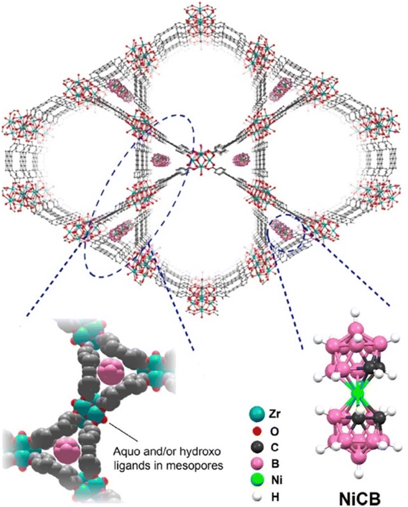 | ||
| Fig. 21 The crystal structure of NiCB@NU-1000 (100 K; only one orientation of NiCB in the triangular channels is shown for clarity). Triangular channels of NiCB@NU-1000 are also shown in the space-filling model to present the close interaction between NiCB and three surrounding pyrenes. H-atoms have been omitted for clarity. The structure of NiCB is also presented. Reproduced with permission from ref. 169. Copyright 2018, The American Chemical Society. | ||
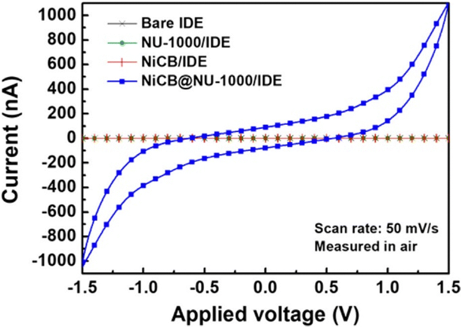 | ||
| Fig. 22 I–V curves of the bare IDE, NU-1000/IDE, NiCB/IDE, and NiCB@NU-1000/IDE. Reproduced with permission from ref. 169. Copyright 2018, The American Chemical Society. | ||
The enhancement of electrical conductivity of host MOFs through encapsulation of π-conjugated guest species was also studied by Guo et al.,92 who attempted to modulate the electrical conductivity of the porous BMOF [Zn2(TCPB)(BPDPNDI)] (BPDPNDI = N,N′-bis(4-pyridyl)-2,6-dipyrrolidyl naphthalenediimide and TCPB = 1,2,4,5-tetrakis-(4-carboxy-phenyl)benzene) through encapsulation of multiple organic moieties. (Fig. 23).
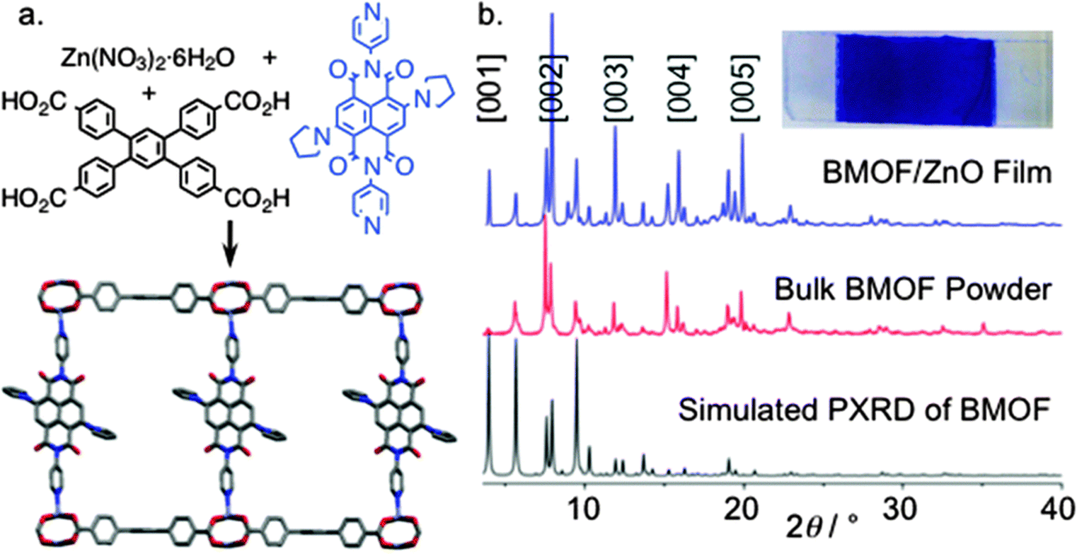 | ||
| Fig. 23 (a) Solvothermal synthesis and crystal structure of BMOF [Zn2(TCPB)(BPDPNDI)]. (b) XRPD profiles of BMOF. Inset: Photograph of a blue BMOF/ZnO film. Reproduced with permission from ref. 92. Copyright 2016, The Royal Society of Chemistry. | ||
In order to measure the electrical conductivity, thin films of the MOF have been prepared on ZnO-coated substrates prepared by spin-coating an EtOH solution of ZnO on FTO and glass slides. The authors observed that during thin-film fabrication, the MOF is selectively deposited on ZnO-coated areas but not on the FTO or glass surfaces. This fact is attributed to the covalent interaction of the tetracarboxylate moieties with the oxide surface. The electrical conductivity was measured by the four-contact method using Au-electrodes. In order to enhance the electrical conductivity, the thin films were immersed in different solutions containing MV2+, 1,5-difluoro-2,4-dinitrobenzene (DFDNB), dinitrotoluene (DNT) or C60. Interestingly, MV2+@BMOF shows a 35 times enhancement of the electrical conductivity (2.3 × 10⁻⁵ S cm−1) compared to the parent BMOF (6 × 10⁻⁷ S cm−1) (Fig. 24).
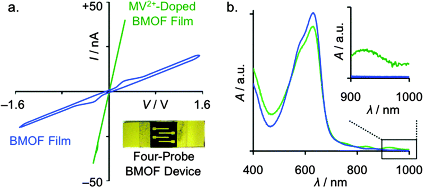 | ||
| Fig. 24 (a) I–V plot of BMOF/ZnO-glass devices (inset) before (blue line) and after (green line) doping with MV2+ for 70 h. (b) Vis-NIR spectra of a BMOF/ZnO film before (blue) and after (green) doping with MV2+. The latter shows new CT bands in the NIR region indicating π-donor/acceptor CT interactions between BPDPNDI ligands and MV2+ guests. Reproduced with permission from ref. 92. Copyright 2016, The Royal Society of Chemistry. | ||
For DFDNB@BMOF (3.5 × 10⁻⁶ S cm−1) and DNT@BMOF (1.5 × 10⁻⁶ S cm−1), there is significant enhancement of the electrical conductivity values but, in contrast, for C60@BMOF, it remains almost constant (4 × 10⁻⁷ S cm−1). The authors have proposed that increasing the π-acidity of the guest molecules (MV2+ > DFDNB > DNT) increases the donor–acceptor interaction between the host and guest moieties, contributing to the enhancement of the electrical conductivity.92 The appearance of a charge transfer band in the NIR region confirmed the presence of charge transfer interaction between the BPDPNDI pillars and the intercalated MV2+ guests (Fig. 24).
Fischer and co-workers have studied the impact of donor–acceptor charge transfer interactions on the electrical conductivity of two isostructural MOFs: M2TTFTB, (TTFTB4− = tetrathiafulvalene tetrabenzoate and M = Zn2+ and Cd2+) through encapsulation of redox-active tetracyanoethylene (TCNE) (Fig. 25). Both MOFs possess a 3D coordination network with π-stacking interactions among the TTFTB4− moieties forming 1D channels. During the formation of the MOF through metal–ligand self-assembly, the ligand oxidizes and the resultant MOF shows a semiconducting behaviour. Due to the loss of single crystalline nature during activation, the TCNE loading was done by using a powder sample. A number of TCNE@MOFs for both frameworks were prepared by heating homogeneous mixtures of TCNE and MOF samples in different ratios varying both the temperature and the heating period. The loading of TCNE within the MOFs was initially confirmed by the colour change from dark red to black. XRPD and SEM analyses indicate that the incorporation of TCNE does not alter the crystallinity and morphology of the MOFs. Pawley fitting shows that the incorporation of guest TCNE reduces the intensity of the peaks belonging to the π-stacked TTFTB linkers and such a decrease in intensity with increasing the amount of TCNE also clearly dictates the partial oxidation of TTFTB4− moieties. Such encapsulation also reduces the porosity of both frameworks. IR and Raman spectral analyses of TCNE@MOFs clearly show a charge transfer interaction with the formation of TCNE˙ and TCNE− as well as TTFTB+ and TTFTB2+. The appearance of such charge transfer is responsible for the increase in the electrical conductivities of TCNE@MOFs when compared with the parent frameworks.170
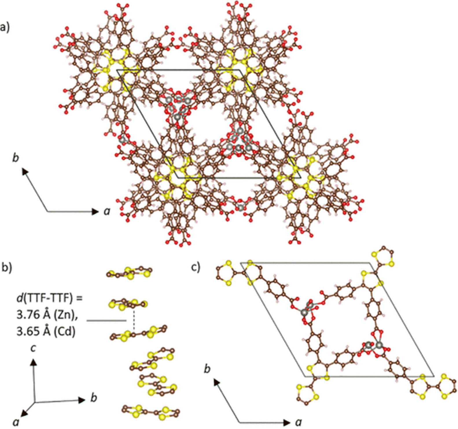 | ||
| Fig. 25 (a) The crystal structure of isostructural M2TTFTB (M = Zn, Cd) MOFs along the c axis. (b) Infinite helical π-stacks of TTFTB units within M2TTFTB aligned along the c-axis. (c) Illustration of the coordination of TTFTB linkers to the rod-shaped SBUs of corner-sharing ZnO6 octahedra. Noncoordinating TTFTB benzoate groups are omitted for clarity. Colour code: C = brown, H = white, O = red, S = yellow and M (here Zn) = silver spheres. Reproduced with permission from ref. 170. Copyright 2005, Elsevier. | ||
Halogens have also a significant impact on the electrical conductivity of the host MOF structure. Thus, Gupta and co-workers have shown an enhancement of the electrical conductivity of Cu[Cu(pdt)] (pdt = pyrazine-2,3-dithiolate) through encapsulation of bromine. Bromine encapsulation was performed in the vapour phase and caused a simultaneous change in cell dimension as well as oxidation of CuII to CuIII with formation of Brx−@CuII[CuII(pdt)2]1−x [CuIII(pdt)2]x. The combination of bromine doping as well as redox hopping between CuII and CuIII centres promotes a 10 times enhancement of the electrical conductivity (measured with the two probe method on pressed pellets) from 1.4 × 10⁻⁴ S cm−1.171
In another case, Zhang et al. have encapsulated Ru(bpydc)34− (H2bpydc = 2,2′-bipyridine-4,4′-dicarboxylic acid) within the channels of three isostructural MOFs M3(HITP)2 (where M = Co, Ni and Cu; HITP = 2,3,6,7,10,11-hexaiminotriphenylene) by the grafting method. Ru(bpydc)34− moieties are bonded to the metal nodes within the host MOFs. Such grafting of the guest coordination complexes enhances the electrical conductivity of the frameworks. The electrochemical impedance analysis shows that the resistance value of Ru@Ni3(HITP)2/GCE (136.8 Ω) is lower than that of Ru@Cu3(HITP)2/GCE (346.1 Ω) and Ru@Co3(HITP)2/GCE (423.9 Ω). Similarly, the electroluminescence of Ru@Ni3(HITP)2/GCE is higher than that of the other two MOFs.172
2.3 Organic polymer-based guests
Following their discovery in 1920,173 the synthesis of organic polymers, bearing repetitive building blocks, has experienced extraordinary development thanks to their countless applications in many different fields. Since the mid-1990s, controlled polymer synthesis in terms of size, dimension, molecular weight, etc. has gained much attention. In this regard, the combination of polymer chemistry with coordination chemistry may create a new generation of novel functional materials. Thus, the integration of polymers within the channels of MOFs has become a major focus in order to combine the novel functionalities of MOFs with the useful properties of polymers.The encapsulation of polymers within the nano-porous channels of MOFs provides an emerging category of materials with a wide variety of applications. The confined polymer chains are affected by their orientation, conformational arrangement, molecular weight, regularity, polymer composition, etc. This host–guest effect is double since, on one side, within the confinement space, polymers show properties different from those of their bulk phases. On the other side, the encapsulation of polymers within the nano-channels of frameworks may have a significant effect on the physical and chemical properties of the host MOF.
Encapsulation of organic conducting polymers has been done using several methods. In most cases, monomers are loaded within the channels of the MOF using an in situ synthetic method like a ‘ship-in-a-bottle’ approach. The small monomers can be easily loaded within the channels of the framework and then different types of polymerization methods like radical, electrochemical, ionic, ring opening methods, etc. are applied to form the extended polymeric chains within the channels of the MOF. The so-formed polymeric chains are trapped within the channels and thus cannot be easily released. In some cases, the monomers are loaded by soaking the MOF in the monomers or in a solution of the monomers in different solvents. Subsequently, the loaded guest monomers are converted to polymers. Recently, grafting has emerged as a new method to load the monomers in the MOF. In this case, pre-functionalized MOFs, in both, ligand and metal nodes, interact with a monomer or oligomer having a counter-functional site, facilitating the incorporation of the guest species through strong host–guest interaction within the channels of the framework. The loaded guests can attach to the ligand site by covalent bonding or to the metal site by coordination bonds. These grafted monomers/oligomers can be afterward polymerized within the channels. In a few cases, the polymer chains are directly loaded within the channels of the MOFs. MOFs are soaked in a solution of the polymer or in a melted polymer leading to the direct insertion of the polymer chains within the channels. Such direct insertion becomes feasible due to strong interactions between the polymer chains and the pore walls.
As expected, most of the attempts to increase the electrical conductivity of polymer-doped MOFs have been performed with π-conjugated organic polymers since they are well-known for their electrical conducting properties174 and their applications in many different electronic devices. Therefore, the incorporation of conducting polymers like PEDOT (polymer of 3,4-ethylenedioxythiophene),175 polyaniline (PANI),176 polypyrrole (PPy),177 polythiophene (PTh),178 polyacetylene (PA),179etc. into different MOFs, is expected to increase their carrier density leading to higher conductivities for the guest@MOF materials.
Later, Kitagawa et al. encapsulated PEDOT within the void space of MIL-101(Cr) in a two-step synthesis: adsorption of the monomer 3,4-ethylenedioxythiophene (EDOT) and then I2-mediated oxidative polymerization (Fig. 26). The polymerization within the cavities of the parent MOF was characterized by ATR-FTIR, XRPD, MALDI-TOF, X-ray fluorescence (XRF) and adsorption studies. These authors showed that PEDOT@MIL-101(Cr) has 108 times higher electrical conductivity (1.1 × 10⁻³ S cm−1) than the parent MOF (∼10−11 S cm−1) and, furthermore, that the conductivity of PEDOT@MIL-101(Cr) varies with the amount of loaded polymer. The conductivity of PEDOT@MIL-101(Cr) is also higher than that observed with other polymers, such as polypyrrole and polyaniline, encapsulated within MIL-101(Cr). The authors also showed that PEDOT@MIL-101(Cr) is more conducting than PEDOT encapsulated within La(1,3,5-benzenetricarboxylate). These results demonstrate that the interaction between the polymer and the framework is a key parameter for the enhancement of the electrical conductivity.180
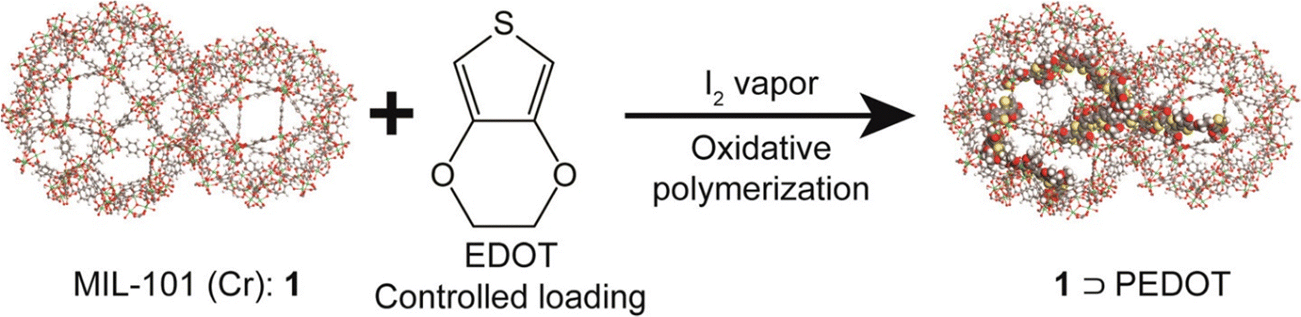 | ||
| Fig. 26 Schematic image for the preparation of PEDOT@MOF. Reproduced with permission from ref. 180. Copyright 2016, The American Chemical Society. | ||
Ballav and co-workers have attempted to modulate the charge transport behaviour of the bi-porous insulator UiO-66 MOF through encapsulation of PEDOT and PPy. UiO-66 MOF was immersed in two different solutions of the monomers and the polymerizations were carried out with I2 and FeCl3 to form UiO-66-PEDOT and UiO-66-PPy, respectively (Fig. 27).181
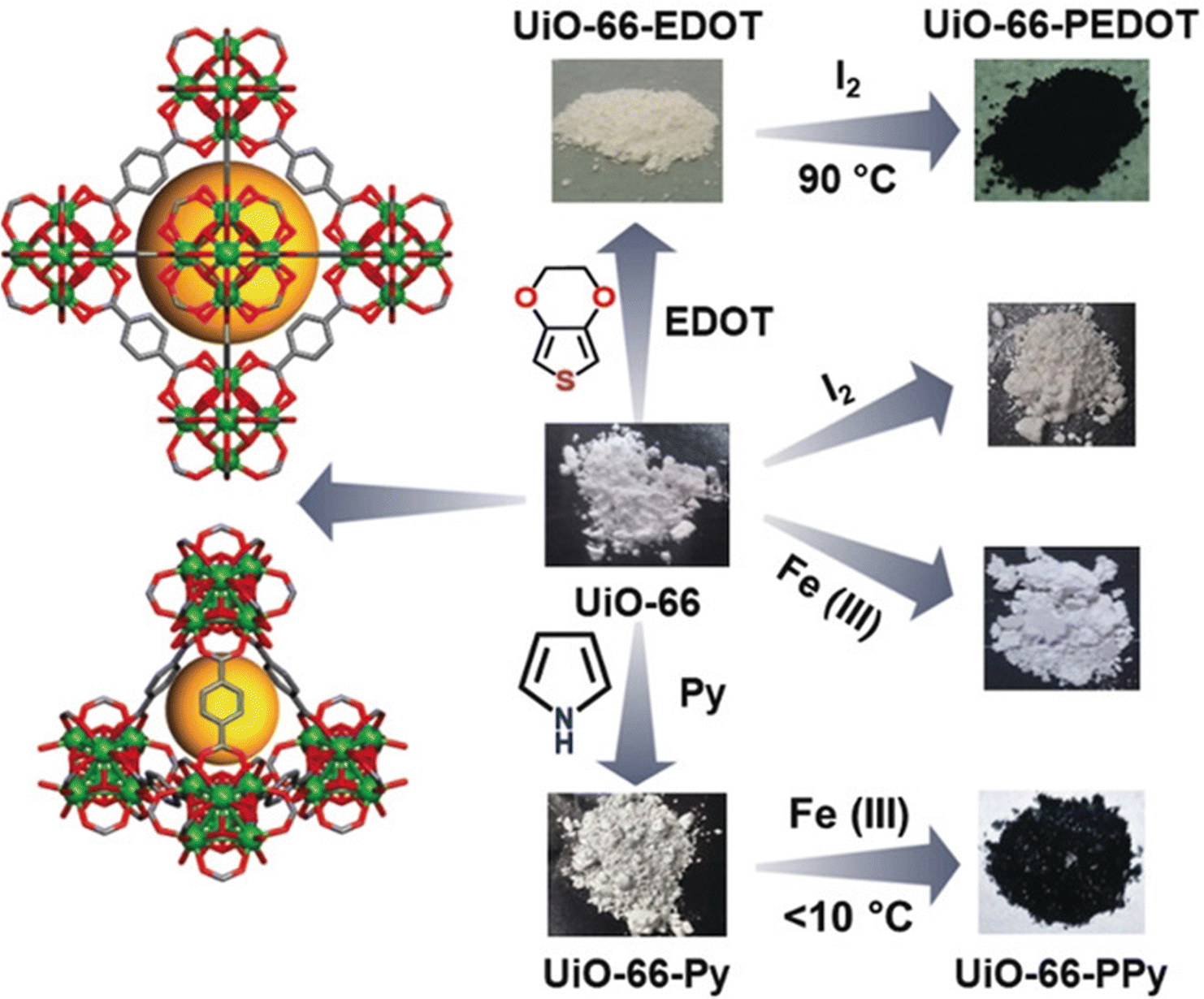 | ||
| Fig. 27 Reaction scheme for the synthesis of UiO-66-PEDOT and UiO-66-PPy. Left panel: Visualizing two different pores in UiO-66 (colour code: green, zirconium; red, oxygen; gray, carbon; hydrogen is omitted for clarity). Right panel: Optical images of products obtained after each step. Reproduced with permission from ref. 181. Copyright 2019, Wiley and VCH. | ||
Incorporation of the polymers within the pores of the framework was confirmed by naked eye colour change, absorption spectra, XRPD analysis, TGA, field emission-SEM, energy dispersive X-ray spectroscopy and gas adsorption analysis. XRPD studies show the retention of crystallinity after polymer formation while N2 sorption analyses indicate that the BET surface area decreases from 1670 m2 g−1 (in UiO-66) to 1150 m2 g−1 (in UiO-66-PPy) and 960 m2 g−1 (in UiO-66-PEDOT). Four-probe electrical conductivity studies show room-temperature conductivity values of 2 × 10⁻² S cm−1 and 10−3 S cm−1 for UiO-66-PPy and UiO-66-PEDOT, respectively (Fig. 28).
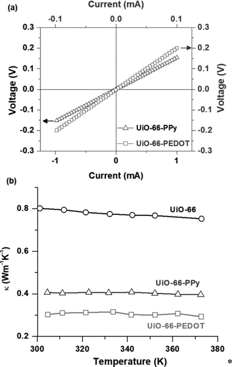 | ||
| Fig. 28 (a) I–V plots of UiO-66-PPy (triangles) and UiO-66-PEDOT (squares) recorded with the four-probe configuration. (b) Thermal conductivity as a function of temperature for UiO-66 (circles), UiO-66-PPy (triangles), and UiO-66-PEDOT (squares). Reproduced with permission from ref. 181. Copyright 2019, Wiley and VCH. | ||
The authors also measured the electrical conductivity of a physical mixture of UiO-66 with the bulk polymers and observed that their conductivities vary between 10−6 and 10−7 S cm−1. These conductivity values are also different from bulk PPy and PEDOT polymers. The authors suggested that the enhancement of the electrical conductivity is due to the synergistic interactions between the conjugated polymer and the host framework.181
Polymeric chains of PEDOT have also been obtained by Wang et al. within the channels of the MOF [Zn2(1,4-ndc)2(dabco)], (where H2-1,4-ndc = 1,4-napthalenedicarboxylic acid and dabco = 1,4-diazabicyclo[2.2.2]octane). Electrical conductivity measurements show that PEDOT@MOF is a better electrical conductor than the pristine MOF, and similar to bulk PEDOT.182
Saha and co-workers have loaded two different types of conducting polymers (PPy and PEDOT) in the channels of an insulating Zn-dpzNDI MOF (dpzNDI = dipyrazolate-naphthalenediimide) to modulate their electrical conductivities.183 The MOF contains large pores in the activated form and π-acidic NDI ligands hard to oxidize. A microcrystalline sample of the framework was immersed in a diethyl ether solution of EDOT and then polymerized in the presence of I2. The polymerization is verified by the naked eye colour change from orange to black. In a similar manner, PPy was loaded into the pores of the same MOF. XRPD studies indicate the retention of crystallinity after polymerization and N2 adsorption studies indicate that the porosity of PEDOT@MOF (28 m2 g−1) and PPy@MOF (283 m2 g−1) is much smaller than that of the parent MOF (1528 m2 g−1). TGA shows that the polymer-loaded MOFs are stable above 300 °C, in contrast with the bulk polymers that degrade at around 100 °C. Two-probe conductivity measurements show that both PEDOT@MOF and PPy@MOF are semiconductors with room-temperature conductivities of 1.8 × 10⁻⁷ and 2.5 × 10⁻⁵ S cm−1, respectively. The conductivity of physical mixtures of the MOF with the polymers is lower. This result strongly demonstrates that a co-operative interaction between the MOF and the polymers is responsible for the enhancement of the electrical conductivity.183
Recently, Salcedo-Abraira et al. synthesized PEDOT@MIL-100(Fe) using a two-step method: adsorption and oxidative polymerization in the presence of FeCl3. They have shown a 100 times increment of the electrical conductivity of the parent MOF upon polymerization of EDOT.184
PEDOT has also been prepared by Mohmeyer et al. on the surface of a Zr-based framework [Zr(bzpdc)]n (where H2bzpdc = benzophenone-4,4′-dicarboxylic acid) with a two-dimensional structure and photoreactive free keto-groups. Zr-bzpdc MOF was immersed in EDOT and irradiated by UV LED at a wavelength of 365 nm under Ar to initiate the ketyl radical formation at the keto-group of the bzpdc moiety of the framework. The ketyl radical reacts with the ethylene moiety of EDOT, resulting in the covalent attachment of EDOT to the MOF, leading to the desired polymerization. Polymer formation was identified with the colour change from colourless to dark brownish. XRPD study shows that such grafting does not change the crystalline nature of the framework. Gas adsorption studies indicate a decrease in porosity after polymerization. Electrical conductivity measurements, carried out by the van der Pauw method, indicate that the conductivity increases from 10−6 S cm−1 in the pristine Zr-bzpdc MOF to 10−3 S cm−1 after 24 h.185
Interestingly, simultaneous enhancement in both electrical conductivity and stability of an insulating and unstable MOF through encapsulation of PEDOT has been reported by Zhang and co-workers. The MOF Ni2(NDISA) (NDISA = naphthalenediimide N,N-disalicylate) is insulating in nature (σ = 10−10 S cm−1) and undergoes structural decomposition upon desolvation. The encapsulation of PEDOT enhances both the stability and the electrical conductivity. The conductivity value becomes ∼1.1 × 10⁻⁵ S cm−1 with 22% wt encapsulation and ∼10−4 S cm−1 with ≥ 33% wt encapsulation of PEDOT.186
A huge enhancement of the electrical conductivity through encapsulation of PPy chains within the 1D channels of the MOF [Zn3(D,L-lactate)2(4-pyridylbenzoate)2] has been reported by Wang et al. (Fig. 29).189 This MOF was immersed in neat Py resulting in the uptake of Py within the channels of the framework. The oxidative polymerization was carried out in the presence of 0.05 M I2 at −16 °C over 72 hours in hexane solution. The polymerization was monitored by visual colour change and absorption spectroscopy, IR spectra, XRPD and SEM analyses. SEM micrographs of the isolated PPy chains from the MOF show that the chain length of PPy moieties is within the range of 20–30 nm. PPy@MOF shows 105 times higher electrical conductivity (10−2 S cm−1) than bulk PPy (10−7 S cm−1) and 10 times higher than I2@MOF. Furthermore, these authors have also reported that isolated PPy chains have five times higher electrical conductivity than PPy layers. The improved conductivity in PPy@MOF might be attributed to the cooperative electrical conductivity resulting from the confined PPy molecule chains surrounded by a π-donor type environment189
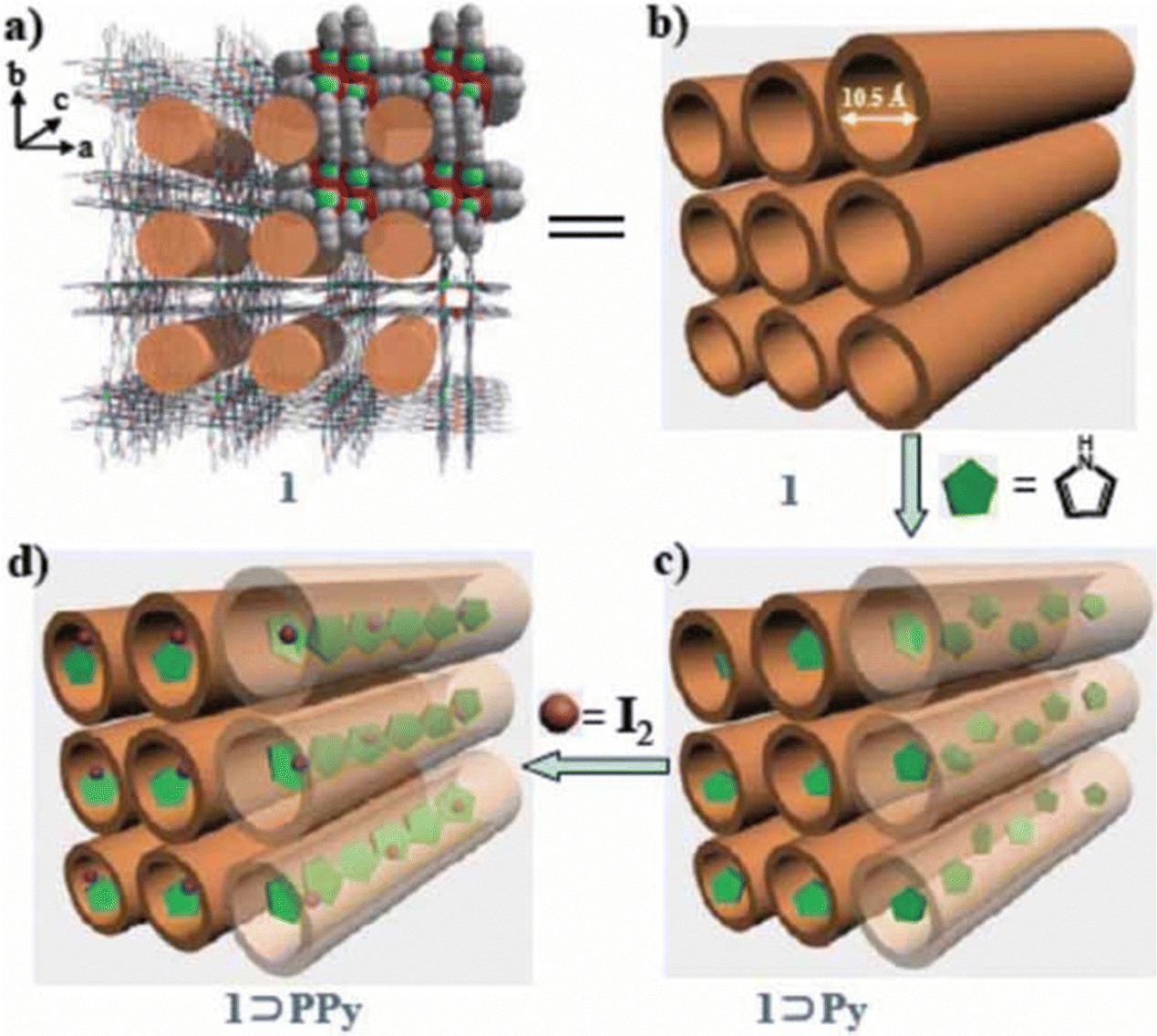 | ||
| Fig. 29 Schematic illustration for the formation of PPy in the channels of [Zn3(D,L-lactate)2(4-pyridylbenzoate)2] (1). (a) 3-D open framework of the MOF with 1-nm nanochannels. (b) Framework of the MOF. (c) Encapsulation of Py in the channels of the MOF. (d) Polymerization of Py with iodine. Reproduced with permission from ref. 189. Copyright 2011, Wiley and VCH. | ||
Later, Dhara et al. encapsulated PPy within the porous channels of a Cd-MOF (Cd-MOF = [Cd2(NDC)(PCA)2]·Gx with H2NDC = 2,6-naphthalenedicarboxylicacid, HPCA = 4-pyridinecarboxylic acid and G = guest molecules, Fig. 30) through a two-step method.190 Guest pyrrole (Py) monomer was incorporated into the 1D nanochannels of Cd-MOF and was polymerized to polypyrrole (PPy) with I2 as an oxidant. The host–guest PPy@Cd-MOF shows 109 times higher conductivity (10−3 S cm−1) than the Cd-MOF (10−12 S cm−1) and 104 times higher than I2@Cd-MOF (10−7 S cm−1). Variation of the conductivity with temperature showed a variable range hopping transport mechanism (Fig. 30). The calculated activation energy was ∼0.2 eV. This huge increase in conductivity could be mainly due to non-covalent interaction of guest PPy chains with the host that results in an increase in the electron current across the framework. Hall effect measurement shows n-type semiconductor behaviour of the MOF with high carrier density (∼ 1.5 × 1017 cm−3) and mobility (∼ 8.15 cm2 V−1 s−1).190
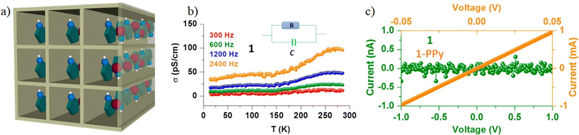 | ||
| Fig. 30 (a) Schematic incorporation of PPy guest inside the Cd-MOF host, (b) Conductivity versus temperature plots obtained from frequency-dependent dielectric measurements of PPy@Cd-MOF (inset: scheme of resistance). (c) Room-temperature I–V plots of Cd-MOF (green) and PPy@Cd-MOF (orange). Reproduced with permission from ref. 190. Copyright 2016, The American Chemical Society. | ||
Ppy has also been inserted in zeolitic-imidazolate frameworks in order to prepare conducting ZIF materials. Thus, Jiao and co-workers reported the polymerization of pyrrole in the void space of ZIF-67.191 Pyrrole monomers are loaded within the pores of the framework by the solvent evaporation method and then polymerization was carried out in the presence of Fe3+. Three different composites were prepared: PZ-1, PZ-2 and PZ-3 with a pyrrole/ZIF mass ratio of 1, 2 and 5, respectively. Unfortunately, the loading of PPy decreases the crystallinity and morphology of the frameworks. Electrical conductivity measurement shows that the conductivity of PZ-3 is 1.5 S cm−1.191
PPy has also been inserted in ZIF-67 using a templated synthetic method by Yuan et al.192 Interestingly, the morphology of the pyrrole-loaded ZIFs is dependent on the amount of pyrrole used during the synthesis. When the pyrrole:2-MIM ratio is 1:1 (2-MIM = 2-methylimidazole), the crystal morphology of the synthesized PZ-1 is dodecahedral, similar to pristine ZIF-67. When this ratio is 5:1, the morphology of PZ-5 changes to truncated dodecahedra with a total of 18 facets (Fig. 31). The number of newly emerged facets increases continuously with increasing the pyrrole:2-MIM ratio, and finally, for a 1:20 ratio, the morphology becomes cubic and remains cubic for any ratio above 1:20.
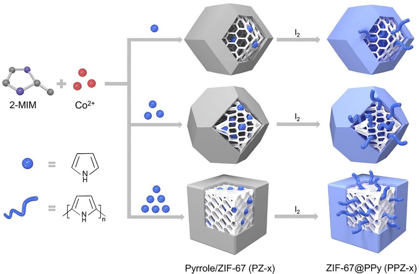 | ||
| Fig. 31 Schematic illustration of the modulation of ZIF-67 crystal morphology by pyrrole and the formation of polymer-reinforced ZIF-67 using I2 as the polymerization initiator. Reproduced with permission from ref. 192. Copyright 2021, Elsevier. | ||
The as-obtained samples of PZ-x were then re-dispersed into an I2-containing methanol solution to polymerize the pyrrole monomers (PPZ-x). Polymerization was monitored using absorption spectroscopy, XRPD analysis and gas adsorption studies. The specific surface area and pore volume of the activated ZIF-67 (1555.5 m2 g−1 and 0.797 cm3 g−1) decrease to 992.1 m2 g−1 and 0.510 cm3 g−1, respectively, for PPZ-20. Four probe conductivity measurements (Fig. 32) show that PPZ-20 has a conductivity value of 0.51 S cm−1, nine orders of magnitude higher than that of the pristine ZIF-67 MOF (4.5 × 10⁻¹⁰ S cm−1) but one order of magnitude lower than pure PPy (6.2 S cm−1).192
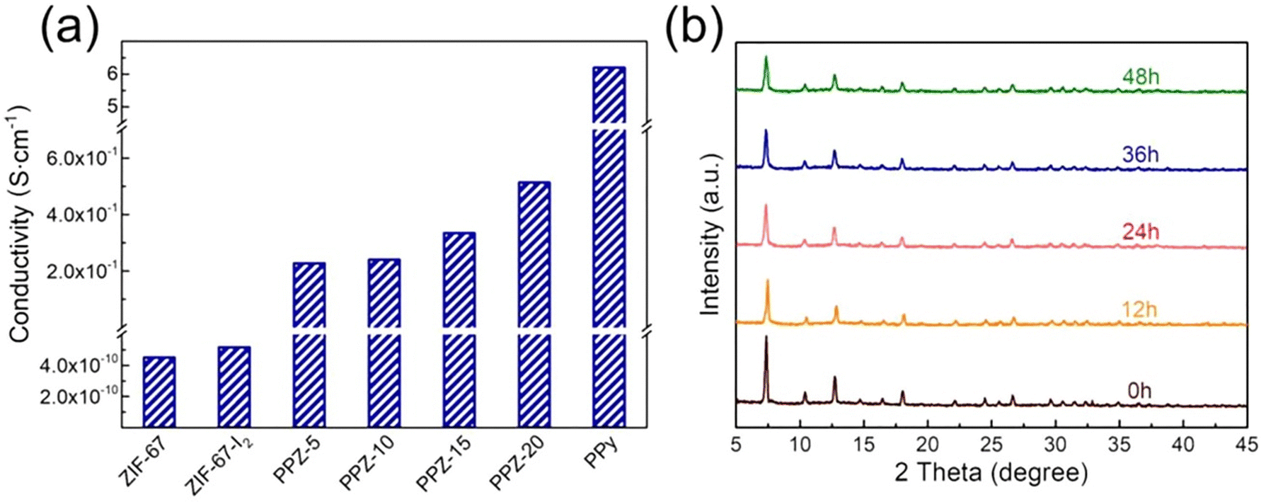 | ||
| Fig. 32 (a) Electrical conductivity of PPZ-x and comparison with ZIF-67, ZIF-67-I2 and PPy. (b) Time-lapse XRD patterns of PPZ-20 immersed in water from 0 to 48 h. Reproduced with permission from ref. 192. Copyright 2021, Elsevier. | ||
Xin and co-workers showed that PPy@MOF (where MOF = [Zr6O16H18][TCPP-Co]2 and H2-TCPP = tetrakis(4-carboxyphenyl)porphyrin) has a higher conductivity (1.08 × 10⁻⁹ S cm−1) than the parent MOF (3.9 × 10⁻¹⁰ S cm−1).93 In some cases, conductive PPy-loaded MOFs have also been used for electrocatalytic applications. Thus, Fang and co-workers reported the enhancement of the electrical conductivity of a 3D porous MOF: {H2TCPP[AlOH]2(DMF3(H2O)2)} (where H2TCPP = 5,10,15,20-tetrakis(4-carboxyphenyl)porphyrin) through incorporation of PPy within the pores of the framework. Furthermore, the resultant PPy@MOF shows an excellent CO2 reduction capacity.193
Very recently, Vello and co-workers have encapsulated PPy within thin films of HKUST-1. The SURMOF of HKUST-1 was fabricated on SiO2/Au electrodes through nanomembrane origami technology. The monomers of Py were encapsulated in the vapour phase within the porous channel of HKUST-1 in the SiO2/Au/HKUST-1/Au devices followed by in situ polymerization to obtain PPy@HKUST-1. The successful encapsulation was monitored by XRPD analysis, Raman spectroscopy, AFM and elemental characterizations. I–V measurement clearly indicates the enhancement of electrical conductivity of the heterojunctions. The conductivity value varies from 2 × 10⁻⁸ to 5 × 10⁻⁸ S cm−1 with the temperature increasing from 180 to 300 K.194
Shao et al. have developed a composite PANI@MIL-101(Cr) by two-step methods: adsorption of aniline within the MOF and then polymerization (Fig. 33). At lower concentrations, the polymers are encapsulated within the pores of the MOF; at higher concentrations, the polymer grows on the surface of MOF particles. IR spectra clearly indicate that N–H groups on the polymeric chains are coordinated with the coordinatively unsaturated Cr(III) centres in addition to the presence of π⋯π/N–H⋯π interactions. SEM and XRPD studies indicate that the morphology and XRD patterns do not change significantly at low polymer loadings although, upon high loadings, substantial changes occur. N2 adsorption analysis indicates that the BET surface area of PANI@MIL-101(Cr) is much smaller than the pristine MIL-101(Cr) due to the filling of the pores of the MOF with PANI. These authors have also shown the continuous enhancement of electrical conductivity by increasing the amount of encapsulated PANI within the pores, with a maximum value of 0.55 S cm−1 for 20% loading.94
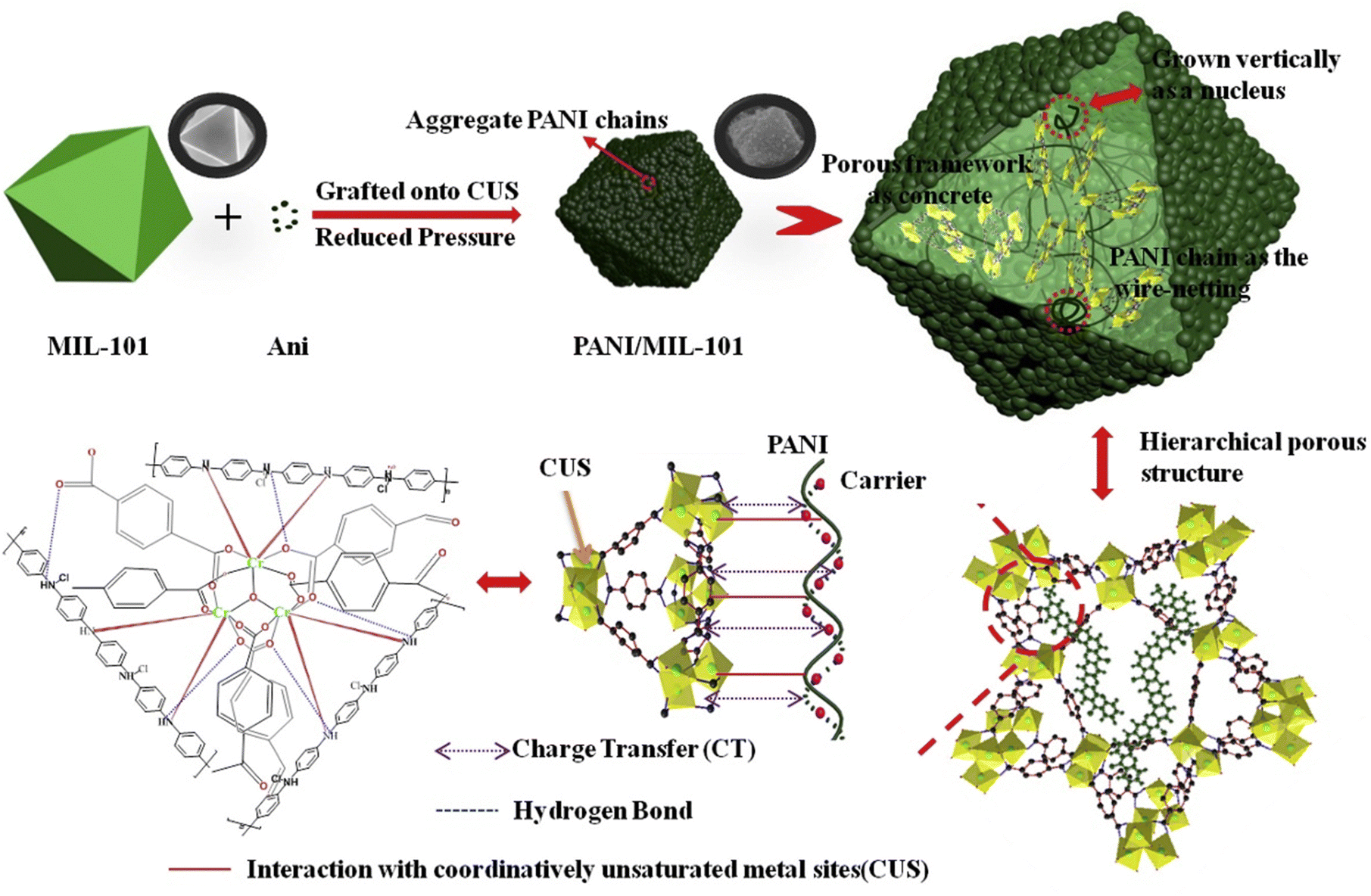 | ||
| Fig. 33 Schematic illustration of the fabrication process and the interaction between PANI and MIL-101(Cr). Reproduced with permission from ref. 94. Copyright 2018, Elsevier. | ||
Later, they prepared another ec-MOF by encapsulating PANI within a UiO-66 MOF under similar conditions. The electrical conductivity of PANI@UiO-66 is higher than that of PANI itself while the MOF acts as an insulator.195 Lin et al. also prepared a composite material of PANI and UiO-66 with the PANI chains located within the channels as well as on the surface of the material. Conductivity measurements show that the resultant PANI@UiO-66 compound has an electrical conductivity of 2.17 × 10⁻⁴ S cm−1.196
In another example, Xu et al. incorporated doped PANI within the hexagonal channels of three different Co-based MOFs: Co-MOF, Co-MOF-Br and Co-MOF-Ag.197 Co-MOF was synthesized by reacting CoCl2 with 5,5′-(1H-2,3,5-triazole-1,4-diyl)diisophthalic acid (H4L) and pyrazin-2-amine (Pz-NH2). The structural study shows that the MOF contains two different types of channels: hexagonal and triangular (Fig. 34). The hexagonal channels are filled with free Co2+ ions and deprotonated anionic ligands. Single-crystal to single-crystal transformations have been observed for Co-MOF by using two different salts, 1-ethylpyridinium bromide (EtpyBr) or AgNO3, replacing the Co2+ ions and the anionic ligands in the pores.
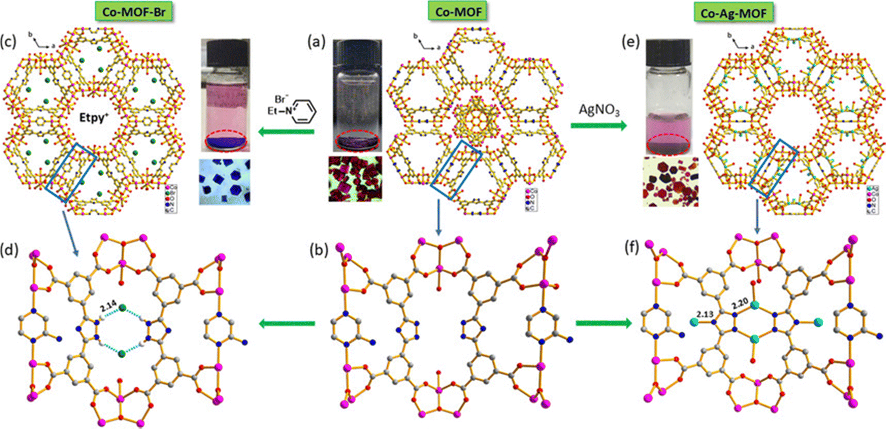 | ||
| Fig. 34 (a), (c) and (e) Crystal structures of Co-MOF, Co-MOF-Br and Co-Ag-MOF and photographs of solutions and crystals before and after metathesis with EtpyBr and AgNO3. (b), (d) and (f) The change of connection mode of L4@, Pz-NH2, SBU1 and SBU2 in MOFs through SC–SC transformation. All H atoms are omitted for clarity. Reproduced with permission from ref. 197. Copyright 2021, Wiley & VCH. | ||
All three MOFs were loaded with doped PANI by immersion in DMF solutions. Four probe electrical conductivity measurements show very high similar conductivity values for PANI@Co-MOF, PANI@Co-MOF-Br and PANI@Co-MOF-Ag (5.9 × 10⁻², 4.8 × 10⁻² and 4.2 × 10⁻² S cm−1 at 300 K, respectively, Fig. 35).197
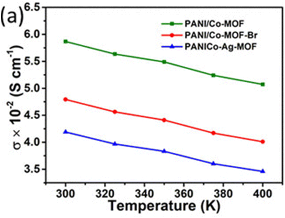 | ||
| Fig. 35 Variable-temperature conductivity of PANI@CoMOF, PANI@CoMOF-Br and PANI@Co-Ag-MOF. Reproduced with permission from ref. 197. Copyright 2021, Wiley & VCH. | ||
:MOF ratio. XRPD study shows that there is no substantial change of peak positions upon polymerization but the intensity of the peaks is reduced. Both the SEM and energy dispersive spectroscopy indicate that the polymers are present within the channels of the MOF and the adsorption analysis shows that the PTTh@MOF has very low void space compared to the parent MOF. Molecular dynamics (MD) simulations show that single and double chains are formed within the channels at low concentrations while at higher concentrations, tri- and tetra-chains are also formed. The polymeric chains within PTTh@MOF·30 (formed by using a w/w TTh:MOF ratio of 30) are assembled by interchain π⋯π interactions. Electrical conductivities of the polyterthiophene-loaded MOFs and of the pristine framework have been measured by flash-photolysis time-resolved microwave conductivity (FP-TRMC) which allows evaluation of the intrinsic charge transport of PTTh chains. Upon excitation by a laser pulse of wavelength of 355 nm, the conductivity of the PTTh@MOF samples increases rapidly compared to the parent MOF. The charge carrier mobility of PTTh@MOF·15 (formed by using w/w Th:MOF ratio of 15) is 0.04 cm2 V−1 s−1. The mobility reaches a maximum of 0.3 cm2 V−1 s−1 for PTTh@MOF·30. The authors suggested that the π-orbital overlap has a key effect for such enhancement of conductivity.198
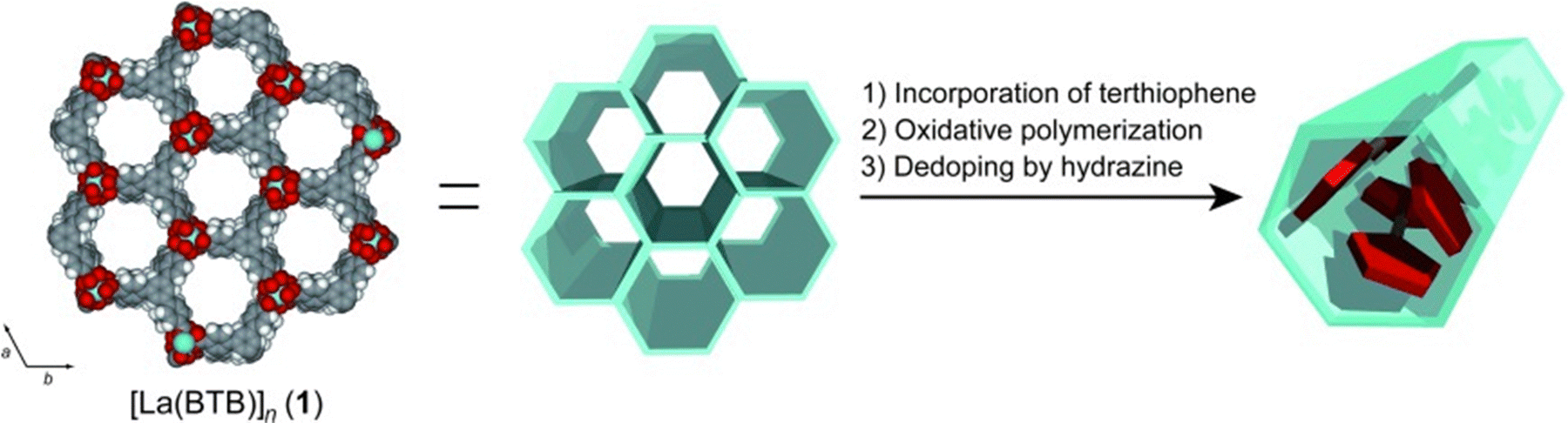 | ||
| Fig. 36 Synthetic strategy for the confinement of unsubstituted polythiophene (PTh) within the 1D channels of the MOF. Reproduced with permission from ref. 198. Copyright 2016, Wiley & VCH. | ||
Polythiophene chains have been prepared by Hupp and co-workers within the porous channels of NU-1000 MOF by using p-thio acid, a building block synthesized by multi-step organic synthesis, composed of five thiophene molecules and a carboxylic acid group connected by an aliphatic chain.199 The p-thio acid precursor was inserted within the channels of the NU-1000 MOF by a post-synthetic method thanks to the interaction of the carboxylate groups that coordinate the metal ions of the Zr6 unit by replacing coordinated water molecules and hydroxide groups (Fig. 37). The incorporation of p-thio-acid within the MOF was characterized by XRPD and adsorption analyses. Polymerization of the coordinated pentathiophene moieties within the channels was performed by electro-polymerization with a concomitant change of colour to green. The change in electrical conductivity was measured by AC impedance analysis. NU-1000 MOF having pentathiophene moieties shows a low conductivity of ∼10−9 S cm−1, while after polymerization, the conductivity increases two orders of magnitude, up to 1.3 × 10⁻⁷ S cm−1.199
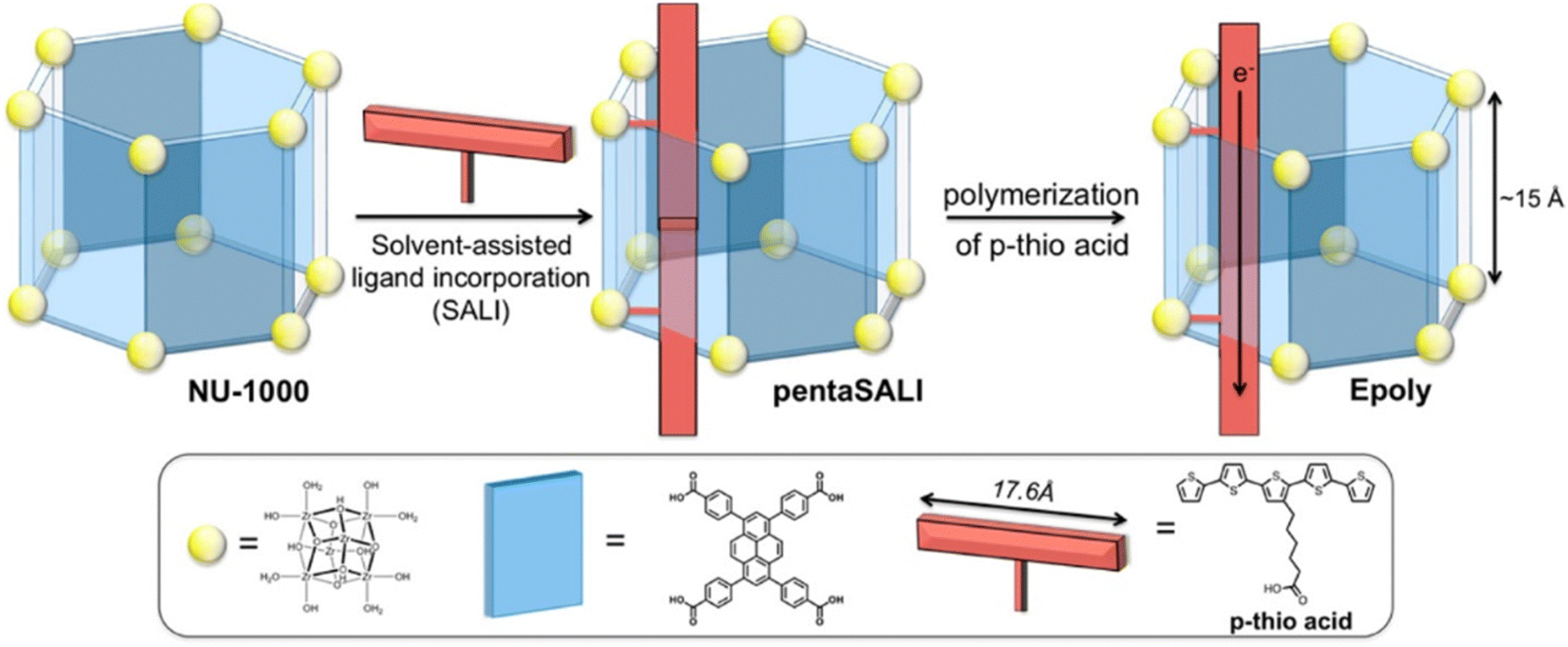 | ||
| Fig. 37 Schematic representation of the synthesis of the PTh@NU-1000 MOF. Reproduced with permission from ref. 199. Copyright 2017, The American Chemical Society. | ||
To date, only Ruben and co-workers have attempted to incorporate PA within the pores of MOFs via potentiostatic electro-polymerization (EP) (Fig. 38 and 39). They electro-polymerized PA using 1-hexyne within the 1D channels of SURMOF [Cu2(BDC)2] (where H2BDC = benzene-1,4-dicarboxylic acid and SURMOF = surface-mounted metal–organic framework). Initially, SURMOF of Cu-BDC has been deposited on Au@SiO2 substrates functionalized by MHDA-SAM (mercaptohexadecanoic acid self-assembled monolayer). A layer-by-layer (LBL) technique is used to obtain monolithic, oriented films with channels within the MOF layer running parallel to the surface. After complete deposition, the thin films were immersed in a dry dichloromethane solution of 1-hexyne. The guest loading was monitored by Raman spectroscopy as the loading generated two characteristic Raman peaks at 2930 cm−1 (assigned to the C–H bond of butyl chains) and 2330 cm−1 (assigned to the C–C triple bond stretches). After loading, the electro-polymerization was performed by keeping 1-hexyne-loaded thin films in a dry dichloromethane solution of 0.1 M tetrabutylammonium hexafluorophosphate (TBAHFP) as a supporting electrolyte.
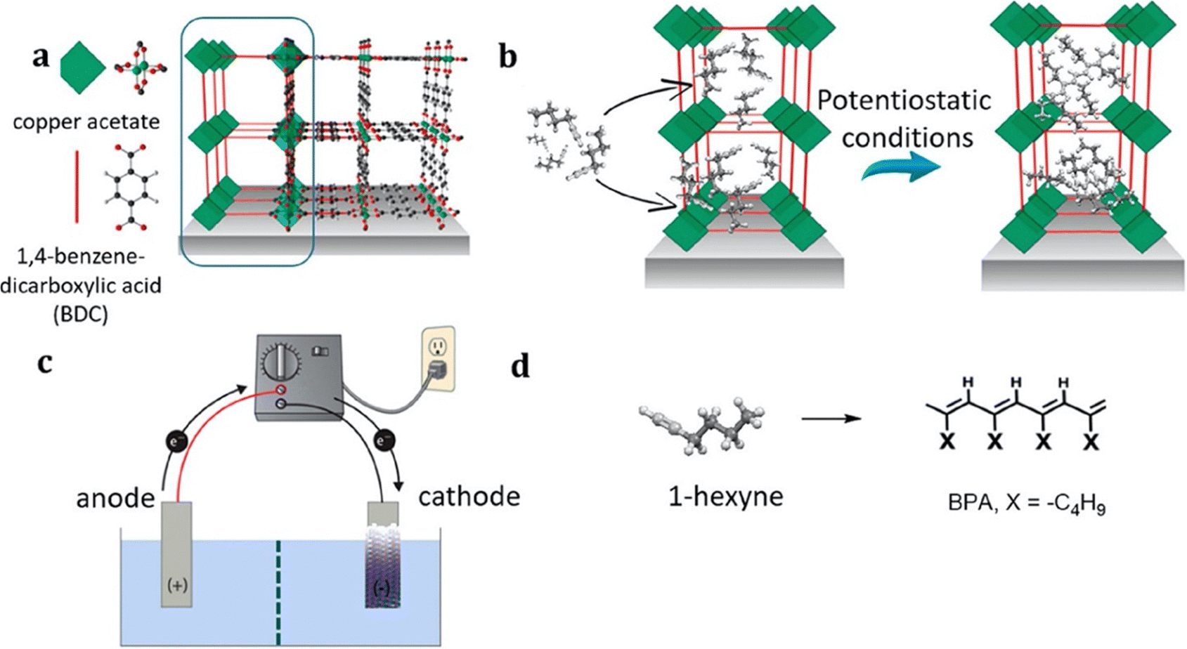 | ||
| Fig. 38 Schematic presentation of the use of Cu(BDC) SURMOF-2 as working electrodes in an electrochemical cell. (a) Side view of Cu(BDC) crystal structure grown along the [001] direction on an MHDA SAM. O = red, Cu = green and C = black. (b) Scheme showing the encapsulation of alkyne monomer and the polymer formation inside the nanochannels of SURMOF-2. (c) Schematic representation of the electrochemical cell. (d) Scheme of polymerization of monosubstituted alkyne (1-hexyne, C6H10). Reproduced with permission from ref. 201. Copyright 2020, The American Chemical Society. | ||
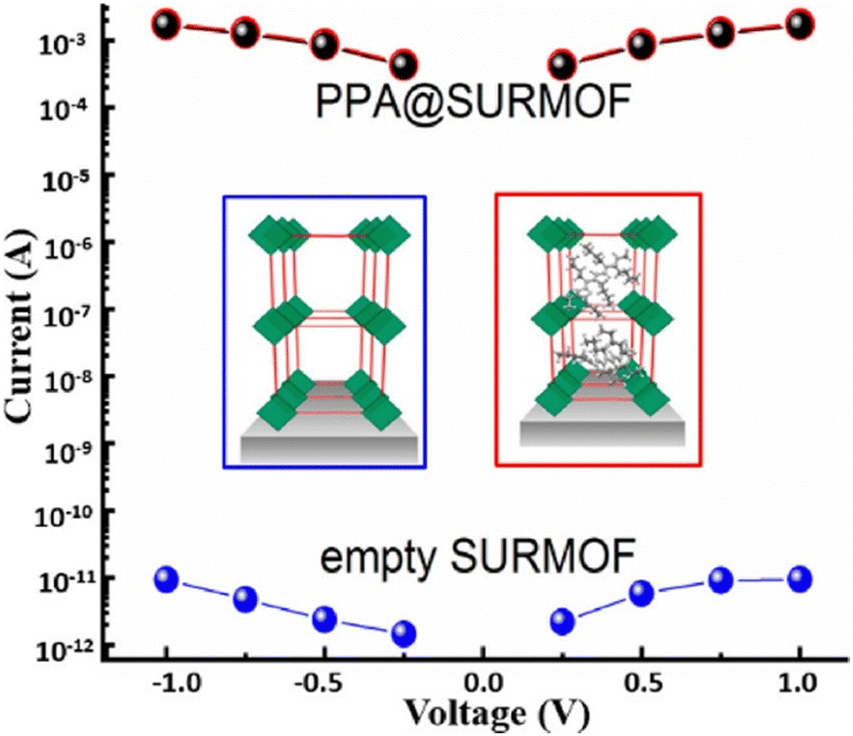 | ||
| Fig. 39 Current–voltage curves before (blue) and after (black) infiltration with 1-hexyne and potentiostatic electro-polymerization (EP). The red data points, virtually identical with the black points, were measured after 3 months after EP where the sample was stored in pure argon at room temperature. Reproduced with permission from ref. 201. Copyright 2020, The American Chemical Society. | ||
The IR peak at 1631 cm−1 is characteristic of the conjugated C![[double bond, length as m-dash]](https://www.rsc.org/images/entities/char_e001.gif) C units within PA and is attributed to the formation of polymeric chains. Raman bands between 1260 and 1600 cm−1 are due to trans-polyacetylene (CC stretching). XRPD, focused ion beam (FIB), SEM, energy dispersive X-ray spectroscopy (EDX) and matrix-assisted laser desorption/ionization (MALDI) analyses clearly demonstrate the polymerization of 1-hexyne molecules to form polyacetylene chains within the pores of the framework. Electrical conductivity measurements show that the conductivity of PA@SURMOF is 9.8 × 10⁻⁴ S cm−1 whereas for the SURMOF, it is only 6 × 10⁻¹² S cm−1. So, the polymerization in the pores has increased the electrical conductivity by 8 orders of magnitude due to both intrachain and interchain charge transport.201
C units within PA and is attributed to the formation of polymeric chains. Raman bands between 1260 and 1600 cm−1 are due to trans-polyacetylene (CC stretching). XRPD, focused ion beam (FIB), SEM, energy dispersive X-ray spectroscopy (EDX) and matrix-assisted laser desorption/ionization (MALDI) analyses clearly demonstrate the polymerization of 1-hexyne molecules to form polyacetylene chains within the pores of the framework. Electrical conductivity measurements show that the conductivity of PA@SURMOF is 9.8 × 10⁻⁴ S cm−1 whereas for the SURMOF, it is only 6 × 10⁻¹² S cm−1. So, the polymerization in the pores has increased the electrical conductivity by 8 orders of magnitude due to both intrachain and interchain charge transport.201
The above-mentioned examples of modification of the conductivity of MOFs by insertion of different types of guests are summarized in Tables 1–3.
| MOF | Guest | Method | σ MOF (S cm−1) | σ Guest@MOF (S cm−1) | σ mechanism | Ref. |
|---|---|---|---|---|---|---|
| PSM = post-synthetic method; GRAF = grafting; CP = conduction pathway. | ||||||
| MIL-101(Cr) | PEDOT + I2 | PSM | 10−11 | 1.1 × 10⁻³ | CP | 180 |
| UiO-66 | PEDOT | PSM | Insulator | 2 × 10⁻² | CP | 181 |
| Zn-dpzNDI | PEDOT | PSM | 10−14 | 1.8 × 10⁻⁷ | CP | 183 |
| [Zr(bzpdc)]n | PEDOT | PSM | 10−6 | 10−3 | CP | 185 |
| ({Zn3(D,L-lactate)2(4-pyridylbenzoate)2}n) | PPy | PSM | — | 10−2 | CP | 189 |
| [Cd(NDC)0.5(PCA)]·Gx | PPy | PSM | 10−12 | 10−3 | CP | 190 |
| ZIF-67 | PPy | PSM | — | 1.5 | CP | 191 |
| [Zr6O16H18][TCPP-Co]2 | PPy | PSM | 3.9 × 10⁻¹⁰ | 1.08 × 10⁻⁹ | CP | 93 |
| ZIF-67 | 20% PPy | PSM | 4.5 × 10⁻¹⁰ | 0.51 | CP | 192 |
| UiO-66 | PPy | PSM | Insulator | 10−3 | CP | 181 |
| Zn-dpzNDI | PPy | PSM | 10−14 | 2.5 × 10⁻³ | CP | 183 |
| UiO-66 | 20% PANI | PSM | Insulator | 0.55 | CP | 195 |
| Co-MOF | PANI | PSM | — | 5.9 × 10⁻² | CP | 197 |
| Co-MOF-Br | PANI | PSM | — | 4.8 × 10⁻² | CP | 197 |
| Co-MOF-Ag | PANI | PSM | — | 4.2 × 10⁻² | CP | 197 |
| NU-1000 | PTh | GRAF | 10−9 | 1.3 × 10⁻⁷ | CP | 199 |
| [Cu2(BDC)2]n | PA | PSM | 6 × 10⁻¹² | 9.8 × 10⁻⁴ | CP | 201 |
3. Fabrication of MOF thin films
For the applications of MOFs in electronic and optoelectronic devices, the fabrication of MOF thin films on conducting substrates is highly desirable.203,204 The fruitful integration can be achieved by establishing strong contacts between the MOFs and the substrates. However, most of the MOFs are synthesized as crystalline powders, hindering their use in device fabrication. Most of the inorganic–organic hybrid MOFs are not as thermally stable as inorganic materials and are not soluble in organic solvents, in contrast to organic compounds. These differences preclude the use of well-established techniques for thin film fabrication.205,206 It is highly important to understand the interfacial interactions and the charge transport mechanism between the substrate and the thin film.206 In order to do so, the first step involves the deposition of thin films on the surface of the substrate. The most important parameters of the deposited thin films are thickness, composition, morphology, crystallinity, homogeneity, robustness, orientation, etc. for their real-world applications.207 Since the properties of thin films may be different from those of the bulk MOFs, the complete characterization of the thin film is also required.206,207 However, the quality of the thin films may vary with the method of deposition.208,209 Thus, it is necessary to gain proper knowledge of the thin film fabrication method. Another important criterion for developing thin films is the proper choice of the substrate. Different materials like silicon, silica, silicon nitride, gold, aluminium, graphite, copper, indium tin oxide (ITO), fluorine-doped indium tin oxide (FTO), etc. have been chosen for this purpose. In some cases, functionalization of substrates like self-assembled monolayer (SAM) formation or polymer coating has been performed to form uniform thin films. There are also a few reports of thin film fabrication using extrinsically conducting MOFs, and, therefore, we describe examples of thin film fabrication of MOFs using both intrinsically and extrinsically conducting MOFs.To date, different methods have been developed for depositing MOF thin films on solid substrates, but it is difficult to use only a particular method for all types of MOFs. Several review articles have highlighted this topic.203–209 Here, we attempt to provide a better understanding of thin film methods to find out the most suitable ones applicable for extrinsically conducting MOFs. We have classified all the methods to fabricate thin films of MOFs into two categories: (a) liquid phase and (b) gas phase.
3.1 Liquid phase processing
Here, the solutions of either pre-synthesized MOF or MOF precursors are used for the thin film fabrication.3.1.1.1 (a) Exfoliation. Liquid phase exfoliation has been done by ultrasonication or ball milling to prepare dispersed thin layers of 2D metal–organic frameworks and coordination polymers very easily, and thus, it is well-accepted to delaminate many types of layered frameworks.210 In this method, a very small amount of sample (∼1–2 mg) is dispersed in a solvent and then delaminated through exfoliation using ultrasonication. The obtained delaminated nano-/micro-flakes are dried by solvent evaporation from the suspension and collected. For the thin film fabrication, the suspension can be drop-cast or spin-coated on the substrate or the obtained dried thin flakes re-disperse in the same or a different solvent and drop-cast on the substrate. The thin films can then be characterized using AFM to analyse the thickness, surface roughness and side flake dimensions. Despite the easy synthesis of nano-flakes and thin film fabrication, this method does not lead to the formation of uniform flakes. Although this method allows the preparation of thin flakes of 2D MOFs, device fabrication with these exfoliated 2D flakes remains a challenge, probably due to the difficulty of transferring and attaching the flakes onto different substrates. Suárez-García et al. have reported the delamination of the spin crossover (SCO) 2D metal–organic framework [Fe(L1)2](ClO4)2 (where L1 = tris(2-(1H-tetrazol-1-yl)ethyl)-amine ligand) (Fig. 40).211
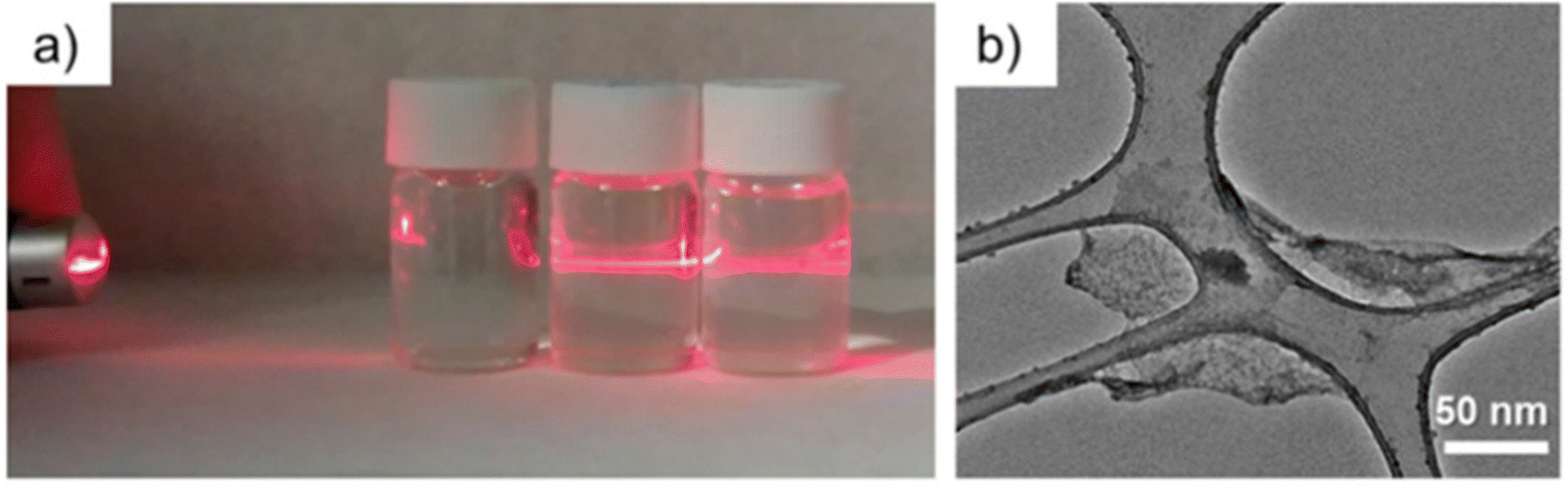 | ||
| Fig. 40 Morphological characterization of the flakes of the SCO MOF [Fe(L1)2](ClO4)2. (a) Tyndall effect demonstration of the colloidal suspension in water. From left to right: the red laser beam remains invisible through the first vial, which contains [Fe(L1)2](ClO4)2 before exfoliation. The scattered laser beam can be observed through the colloidal suspension of flakes immediately (in water, second vial) and a few weeks (in water/ethanol mixture, third vial) after exfoliation; (b) transmission electron microscopy (TEM) image of a single flake, a few hundred nanometres width, obtained after transferring a drop of the same colloidal suspension to the grid. Reproduced with permission from ref. 211. Copyright 2018, the American Chemical Society. | ||
Very good-shaped crystals of this 2D MOF were chosen for the exfoliation and dispersed in different solvents such as water, methanol (MeOH), ethanol (EtOH), dimethylformamide (DMF), acetone ((CH3)2CO), chloroform (CHCl3), toluene (Tol) and tetrahydrofuran (THF) for sonication at room temperature in an ultrasound bath for 4, 6 and 12 h. The exfoliation is monitored by the Tyndall effect. The samples are monitored by dynamic light scattering (DLS) analysis. After 12 h, only the vial containing water showed successful delamination of the layered crystal. Afterwards, the vial was placed in an orbital shaker for 24 h for the correct separation and to increase the exfoliation yield obtaining a final colloidal suspension that is stable for at least one week without any precipitation and/or colour change. The delaminated thin film of the MOF can be deposited on the Si-wafer by drop casting or spin coating of the colloidal solution on the Si-wafer and dried under an argon flow. The dried 2D flakes were further used to measure the spin-crossover behaviour which is similar to the bulk compound.211
Zeng et al. have exfoliated the anionic 2D MOF Eu(dfdmt)2 (where dfdmt = 2,5-difluoro-3,6-dimercaptoterephthalate) into ultrathin and few-layer nanosheets by simple ball-milling. An AFM study indicates that the thickness of the delaminated 2D films is about 0.84 nm for each layer and the lateral dimensions are 324 and 476 nm. HRTEM images reveal the crystalline thin morphology of the flakes with distinct lattice fringes of the thin films. The stability of the delaminated thin films was characterized using XRPD analysis and FT-IR spectroscopy.212
Using ultrasounds with different solvents, Benmansour et al. have shown that it is possible to exfoliate anilato-based mixed-valent FeII/FeIII highly conducting 2D MOFs into nanosheets of a few monolayers (∼7 nm).213
3.1.1.2 (b) Bottom-up deposition. In this method, a substrate is dip-coated into colloidal solutions/suspensions of micro-/nano-sized MOF particles to deposit the thin films on the surface of the substrate. This method is also known as chemical solution deposition (CSD) as the solution contains meta-stabilized MOF particles. The obtained thin films are characterized using XRPD analysis to check their homogeneity and surface topography by AFM and TEM studies. Interestingly, this method leads to the formation of a homogeneous thin film fabrication and also the thickness of the thin films can be controlled by repetition of the coating process. One of the major obstacles is the formation of a metastable state of the MOFs in solution, and thus, it has been used in rare cases. Horcajada and co-workers have deposited the thin film of MIL-89 {[Fe3OCl(muconate)3]·nSolv} on a silicon wafer by this method.214 Initially, they prepared a colloidal solution of MIL-89 NPs by heating the orange mixture of iron(III) acetate and trans-muconic acid in ethanol at 60 °C for 10 min which led to a rapid increase of viscosity and cloudiness of the solution. Afterwards, the side-polished silicon wafer was dip-coated within the cooled colloidal solution for 2 min and then dried at room temperature. The film thickness can be improved through multiple deposition under the same conditions.214 These authors have also obtained thin films of other MOFs such as MIL-101 [Cr3OF(BDC)2(H2O)2]2 and ZIF-8 [Zn(Cu4H5N2)2] with this method. This method allows for the preparation of thin films with controlled size of the MOF particles.215,216
3.1.1.3 (c) Spin coating. The solvothermally synthesized MOF particles can be directly deposited by spin coating a suspension of a MOF in a volatile solvent on the surface of a substrate. The MOF powder is dispersed in a highly volatile solvent, homogenized by sonication and then the suspension is drop-cast on the substrate through the spin coating method. In most cases, a binder is mixed with the MOF particles before drop-casting to improve the adhesion of the MOF particles to the surface. This is one of the oldest methods for the fabrication of thin films and has attracted significant attention for the low cost and simplicity but the formation of a uniform distribution on the surface is questionable. Wong and co-workers have studied the photocatalytic water splitting behaviour of the MOF [La(TTCA)(H2O)]·DMF·H2O (TTCA3− = triphenylene-2,6,10-tricarboxylate, DMF = N,N-dimethyl formamide) by depositing thin films of it on an ITO substrate using Nafion as the binder.217 Similarly, Horiuchi et al. have also deposited thin films of MIL-101(Fe) on FTO glass substrates with Nafion as a binder and studied the photocatalytic activity.218 In some cases, other additives like polymeric binders are used for this purpose. Campbell and co-workers have fabricated HKUST-1 membranes with polyimide P84 by mixing HKUST-1 microcrystals with a solution of the polymer with polymer
:HKUST ratio of 5:1 and then this mixture was cast on the polypropylene non-woven sheets to obtain thin films of thickness ∼250 μm.219
Ho and co-workers have synthesized thin films of MOF-525 by immersing an FTO doped glass substrate in a solution of precursors H4TCPP, benzoic acid, and zirconyl chloride, octahydrate in a two-step method (Fig. 41).220
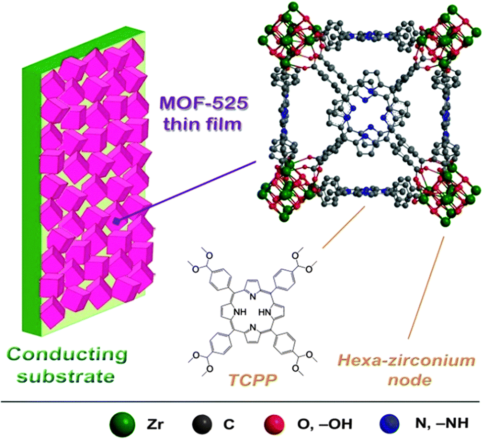 | ||
| Fig. 41 MOF-525 crystal structure and schematic representation of its solvothermally grown thin film. For simplicity, hydrogen atoms are not shown. Reproduced with permission from ref. 220. Copyright 2015, the Royal Society of Chemistry. | ||
The synthesis of the thin film was monitored by XRPD analysis. SEM images reveal that the cubic MOF particles are very uniform, with sizes in the range of 500–1000 nm and that there is a strong adhesion between the MOF particles and the substrate. These authors have demonstrated that the MOF particles remain identical after post-metalation by immersing the thin films into solutions of Co and Zn salts. Energy dispersive X-ray (EDX) spectroscopic analysis clearly identifies the uniform distribution of Zn or Co ions within the particles. They have also demonstrated that the charge diffusion is easier in the parent MOF than post-metalated MOFs as evidenced by cyclic voltamperometry (CV) analysis.220
Thin films of MOF-5 on ZnO-coated FTO glass substrates have been prepared by Wang et al. using a solvothermal method by soaking the substrate in a DMF solution of Zn(NO3)2 and terephthalic acid.221 An attempt with bare FTO was unsuccessful. The formation of a thin film was characterized by XRD and SEM analyses. Tb3+ doping was done by soaking the thin films in DMF solutions of Tb(NO3)3 for 3 days and was characterized by XRD, SEM, EDS and ICP analyses. SEM micrographs clearly show the strong attachment between the MOF particles and the substrate. These doped MOF-5 thin films act as a good luminescent material.221
Recently, Saha and co-workers have developed thin films of a porphyrin-based MOF, namely ZnTCPP (TCPP = tetrakis(4-carboxyphenyl)porphyrin) on ZnO-coated FTO glass slides. DMF:ethanol solution of Zn(NO3)2, TCPP and DMBPY were solvothermally treated at 80 °C for 2 h for initial nucleation, and then, the substrate was immersed in the solution and consequently solvothermally treated at 80 °C for another 30 min. An XRD study shows that the thin films were grown in the [100] direction in contrast to the [001] direction of bulk crystallization. These authors have suggested that the ZnO surface facilitates the thin film fabrication by capturing TCPP struts through –COOH groups and thus directing the film growth vertically on the surface. SEM images revealed that the densely packed rectangular slab-like crystals are vertically oriented on the surface and the thickness is ∼10 μm (Fig. 42). Afterwards, these authors encapsulated C60 within the void space of the MOF by soaking the thin films in a saturated solution of C60 in toluene for seven days. The fullerene-doped ZnTCPP thin films show weaker solar cell photoconversion activity than that of the undoped MOF.222
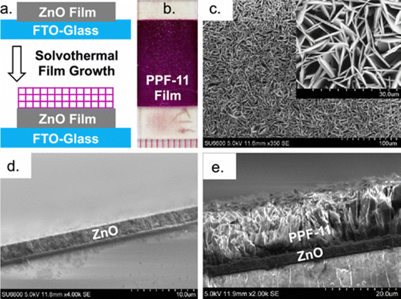 | ||
| Fig. 42 (a) Schematic diagram outlining the solvothermal growth of the PPF-11 film. (b) A photograph of a solvothermally grown PPF-11/ZnO film. (c) Scanning electron microscopy (SEM) images of a PPF-11/ZnO film showing densely packed crystals aligned uniformly on the surface. Cross-sectional-SEM images of (d) a 2.5 μm thick annealed ZnO film and (e) a solvothermally grown 10 μm thick PPF-11 film on the ZnO layer. Reproduced with permission from ref. 222. Copyright 2019, The American Chemical Society. | ||
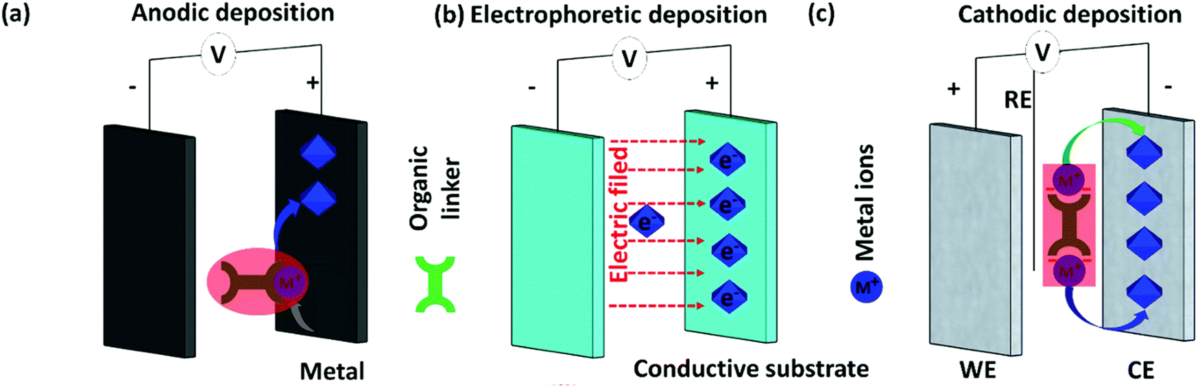 | ||
| Fig. 43 Schematic representation of the electrochemical fabrication of MOF thin films with (a) anodic deposition, (b) electrophoretic deposition and (c) cathodic deposition. Reproduced with permission from ref. 204. Copyright 2017, the Royal Society of Chemistry. | ||
3.1.3.1 (a) Electrophoretic method (EPD). The underlying principle of this method is to use the partial charge present on the surface of the MOFs. The defects at the surface of the MOF crystallites due to missing metal ions or linkers create partial charges at the surface. Under an applied voltage, the MOF particles move towards the electrodes following the charge at the surface. In the electrophoretic method, two electrodes are immersed in a solution containing the MOF as a colloidal suspension. On applying a fixed voltage between the two electrodes, the partial charge on the surface drives the MOF particles towards the oppositely charged electrodes, where they deposit and form thin films. Hupp and co-workers have employed this method to deposit thin films of four different MOFs: NU-1000, UiO-66, HKUST-1 and MIL-53.223 Two FTO electrodes were immersed in toluene solutions of UiO-66 and NU-1000 MOF particles, and then a fixed voltage was applied with different time periods. SEM micrographs indicate that the accumulation on the electrode surface by the MOF particles increases with time of electrophoresis, forming a film of 4–5 μm thickness after 3 h (Fig. 44). The authors have established that the thin films of NU-1000 MOF obtained by this method act as a reversible redox couple similar to NU-901 containing a redox pyrene core. These authors have also developed a micropatterned MOF thin film by combining photolithography with EPD through the consecutive formation of layers of insulating photoresist material, then patterning the photoresist layer by photolithography, later EPD on the bare FTO part and finally removal of the photoresist material.223 Hupp et al. have also prepared thin films of ferrocene derivatized NU-1000 MOF using a similar method and measured their redox behaviour.224
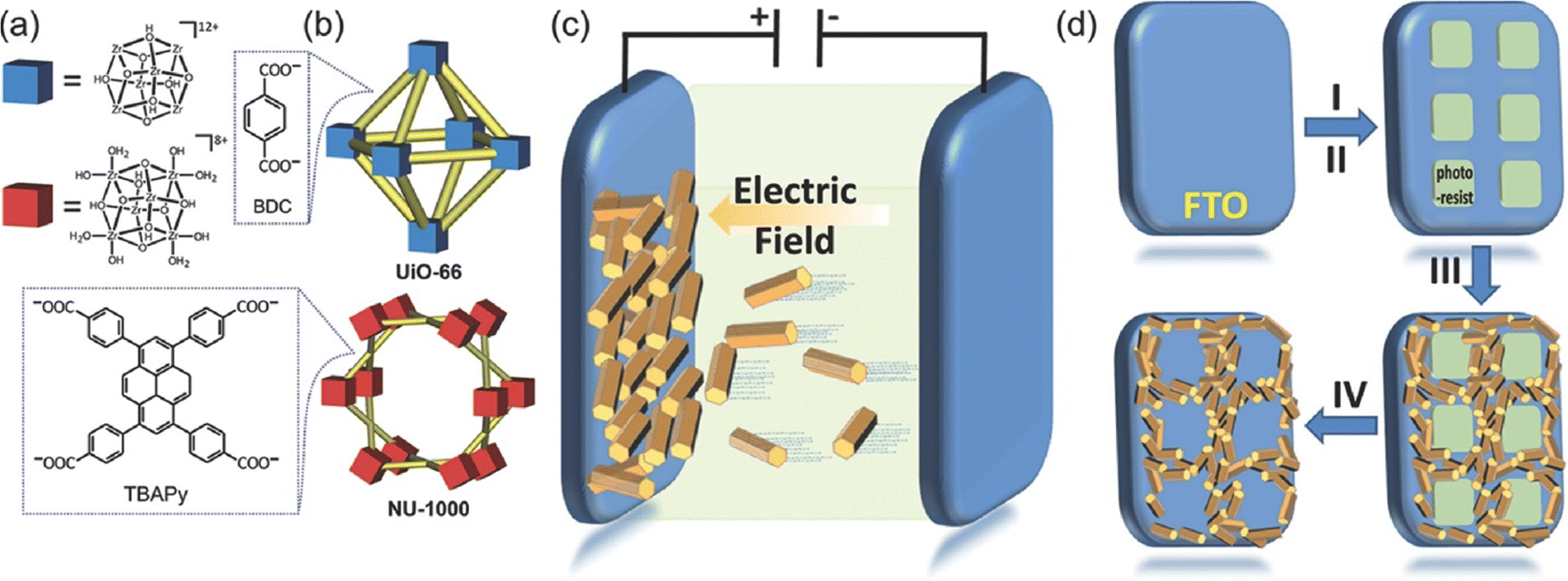 | ||
| Fig. 44 (a) Components of UiO-66 and NU-1000: Zr-containing nodes (blue for UiO-66 and red for NU-1000) and organic linkers. (b) Illustration of the crystal structures of UiO-66 and NU-1000 MOFs. (c) A scheme illustrating the MOF EPD film growth, showing the attraction of charged MOF particles towards an oppositely charged electrode using an applied electric field. (d) Illustration of the patterning of the MOF EPD film procedure: (I) spin coating a layer of photoresist on a bare FTO substrate, (II) using photolithography to create patterned squares of photoresist, (III) deposition of MOF particles on the conductive exposed FTO areas using EPD, and (IV) removal of the remaining photoresist squares to obtain the desired pattern. Reproduced with permission from ref. 223. Copyright 2014, Wiley & VCH. | ||
Zhang and co-workers have developed thin films of ZIF-67 using a similar electrophoretic method by varying the applied voltage from 20 to 60 V to prepare thin films of 1–7 μm thickness within one minute. Later, they converted these MOF thin films into Co9S8 thin films which are further utilized for the degradation of vanillin.225 Recently, Hupp and co-workers have studied the diffusion behaviour of different alkanes with chain length C5–C16 using thin films of ZIF-8 obtained by this method. They have established that the thin films obtained using the EPD method are more porous and allow faster diffusion of alkanes than the thin films obtained using in situ solvothermal methods.226 Nevertheless, there is no report on guest encapsulation within the void space of MOF thin films obtained by this method. Cao and co-workers have developed thin films of Ln3+-doped UiO-66 MOF and have shown their temperature-sensing behaviour.227 In another article, Cao and co-workers have developed thin films of Tb-BTC, Eu-BTC and Eu0.5Tb0.5-BTC MOF (where H3BTC = trimesic acid) by EPD method. In these frameworks, BTC ligands show three different binding modes: bidentate, monodentate and free carboxylate groups that create some charges on the surface that have been utilized for EPD. The thin films were used for detection of Cr3+ and nitrobenzene in the solution phase as well as nitrobenzene in the gas phase.228
3.1.3.2 (b) Anodic deposition. In anodic deposition, a metal electrode is used as the source of the cations and immersed in the solution containing the organic ligand. On applying voltage, the metal oxidizes, generating cations that react with the ligands to generate small MOF particles that grow on the surface of the anode. In some cases, the metal is coated on the surface of non-metallic substrates to be used as an anode. The size of the synthesized MOF particles is dependent on the applied voltage. Increasing the voltage increases the release of cations from the anode, reducing the thickness of the coating. In 2006, Muller and co-workers synthesized a series of MOFs by an electrochemical method using bulk powders.229 Ameloot and co-workers have developed thin films of HKUST-1 by the same method with varying voltages on a copper electrode by immersing two different electrodes in a solution of trimesic acid and methyltributylammonium methyl sulphate (MTBS) as the electrolyte (Fig. 45). The film growth was monitored by XRD and SEM analyses. The SEM micrographs reveal that the size of the synthesized particles can be tuned by modifying the synthetic conditions.230 Later, they have patterned thin film fabrication on the substrate during electrochemical deposition of HKUST-1.231
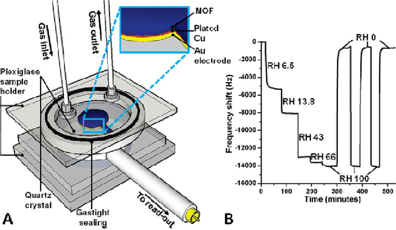 | ||
| Fig. 45 Electrochemically grown [Cu3(BTC)2] coatings in QCMB measurement of water adsorption. (A) Schematic representation of the setup. (B) Signal upon adsorption of water from nitrogen streams at different RH values illustrating reversibility and reproducibility. Reproduced with permission from ref. 230. Copyright 2009, The American Chemical Society. | ||
Campagnol et al. have deposited thin films of MIL-100(Fe) and HKUST-1 by anodic deposition method at high temperatures (110–190 °C) and pressures. They have found that the HKUST-1 particles are formed with an unusual cubic morphology. They have also synthesized MIL-100(Fe) without using any harsh chemicals like strong acid (HF) and conductive salts.232 Schäfer et al. have studied the mechanism of thin film formation for HKUST-1 with the anodic deposition method. They have established that the thin film formation proceeds in two steps: (a) Cu is first oxidized to Cu2O in the presence of O2 and then Cu2O is further oxidized to CuII-BTC in the presence of the linker at the cuprite–electrolyte interface.233 Several other research groups have attempted to synthesize a number of MOFs like ZIF-8, MIL-100(Al) and so on. Stassen and co-workers observed the thin film deposition of UiO-66 MOFs on both the anode and cathode.234 Recently, Hauser and co-workers have synthesized thin films of four different Cu and Zn MOFs, both 2D and 3D, by immersing metal-coated ITO electrodes in the ligand solutions (Fig. 46).235
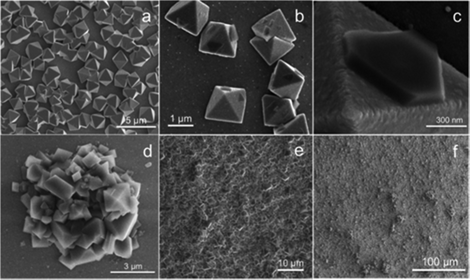 | ||
| Fig. 46 SEMs of HKUST-1 grown on Cu-ITO at 0.75 V: (a) copper octahedra grown by electrodeposition on ITO (−1.0 V for 90 s). (b) and (c) the beginning of HKUST-1 growth on Cu octahedra after 2 min. (d) An isolated copper octahedron covered by MOF crystals after 50 min of growth. (e) Typical film coverage after 50 min of growth. (f) A 0.1 mm2 section of film illustrating the relative smoothness and continuity of the HKUST-1 film after 50 min of growth. Reproduced with permission from ref. 235. Copyright 2010, The American Chemical Society. | ||
3.1.3.3 (c) Cathodic deposition. The cathodic deposition method was first developed by Dinca and co-workers for the thin film fabrication of MOF-5. They used a three-electrode cell where both the working and counter electrodes are used as chemical separators and electron pools but do not participate in the MOF formation. The basic principle of this deposition method is the deprotonation of the organic ligands by reaction with the metal ions near the cathode and this can be done by the electrochemical reduction of oxo-anions like nitrate, perchlorate etc. which consequently produces large amounts of hydroxide ions near the cathode. These hydroxide ions deprotonate the organic ligands for the synthesis of the MOF. For the electrochemical synthesis, Zn(NO3)2, H2BDC (1,4-benzenedicarboxylic acid), (NBu4)PF6 electrolyte was dissolved in 100
:1 DMF–water mixture and a flexible transparent polymer (FTP) electrode was immersed in the solution. A constant potential of 1.6 V was applied for 15 min for the deposition of MOF-5 on the electrode. During the electrochemical reaction, NO3− was reduced to NO2− with subsequent deprotonation of the H2BDC ligands with formation of hydroxide ligands through deprotonation of water in the solution.236 Later, Liu and co-workers prepared thin films of [Eu(HBPTC)(H2O)2]·2DMF (BPTC = benzophenone-3,3′,4,4′-tetracarboxylate) by a cathodic deposition method.227 In this case, they used anhydrides or esters of the ligand with the assumption that increasing hydroxide ion concentration may hydrolyse esters into acids. In the electrochemical cell, enzophenone-3,3′,4,4′-tetracarboxylic dianhydride (BTDA) and Eu(NO3)3 were dissolved in DMF with graphite rod (anode) and FTO (cathode). Applying a current density of 0.4 mA cm−2 for 10 minutes leads to the deposition of thin films on the cathode. They have used these thin films for the luminescence-based detection of carbonate anions in aqueous solution.237 They have also developed thin films of a number of Ln-MOFs by this method and studied their light-emitting behaviour.238 Wang and co-workers have synthesized thin films of terbium succinate by this approach and used them for sensing copper ions in aqueous solution.239
3.1.4.1 (a) Liquid–liquid interfacial method. In this method, two different immiscible liquids are used to dissolve both the metal ions and organic ligands, respectively. Then, one solution is layered over the other and the thin film is formed at the interface of the two solutions. The interface between the two immiscible liquids has been used as a template for thin film formation. Ameloot and co-workers have introduced this technique for the formation of a thin film of HKUST-1.240 Classical HKUST-1 synthesis is done by using two different solvents such as water and ethanol. They have replaced ethanol with octanol to dissolve trimesic acid (H3BTC) and used water to dissolve the copper salt. Both solutions were layered to obtain thin films at the interface. They have also synthesized thin films of ZIF-8 using a similar method. In the same report, they also prepared hollow spheres of HKUST-1 by dispersing the aqueous phase/solution as droplets in an octanol solution. To obtain monodisperse droplets, the aqueous phase was transported through a tapered capillary tube into the co-flowing organic phase. The hollow spheres are formed at the interface when these droplets are moved through the hydrophobic tube and then collected in ethanol. SEM micrographs show that the diameter of such hollow spheres is ∼375 μm.240
Kambe and co-workers have developed thin films of Ni3(BHT) (BHT = benzenehexathiolate) following a similar liquid–liquid interfacial method by using Ni(OAc)2 with NaBr (Na+ acts as a charge compensating counter ion) in the aqueous layer with BHT in DCM. SEM analysis shows that the layers are monolithic in nature with a size of ∼100 μm and a thickness of 1–2 μm (Fig. 47).241 In another example, Huang et al. have developed thin films of Cu-BHT 2D MOF with the same method.242 They observed that, during growth, the thin films change from transparent to opaque. SEM micrographs indicate that the thin films have different morphology on both sides. The upper side is flat and shows no cracks while the other side is highly rough due to the random orientation of the platelike nanosheets. SEM images also show that the thickness of the films is ∼200 nm.242 Recently, Chen and co-workers have synthesized thin films of 2D MOFs, Ag3(BHT) and Au3(BHT), using a similar liquid–liquid interface method.243 Several other research groups have utilized this method to develop thin films of different MOFs.
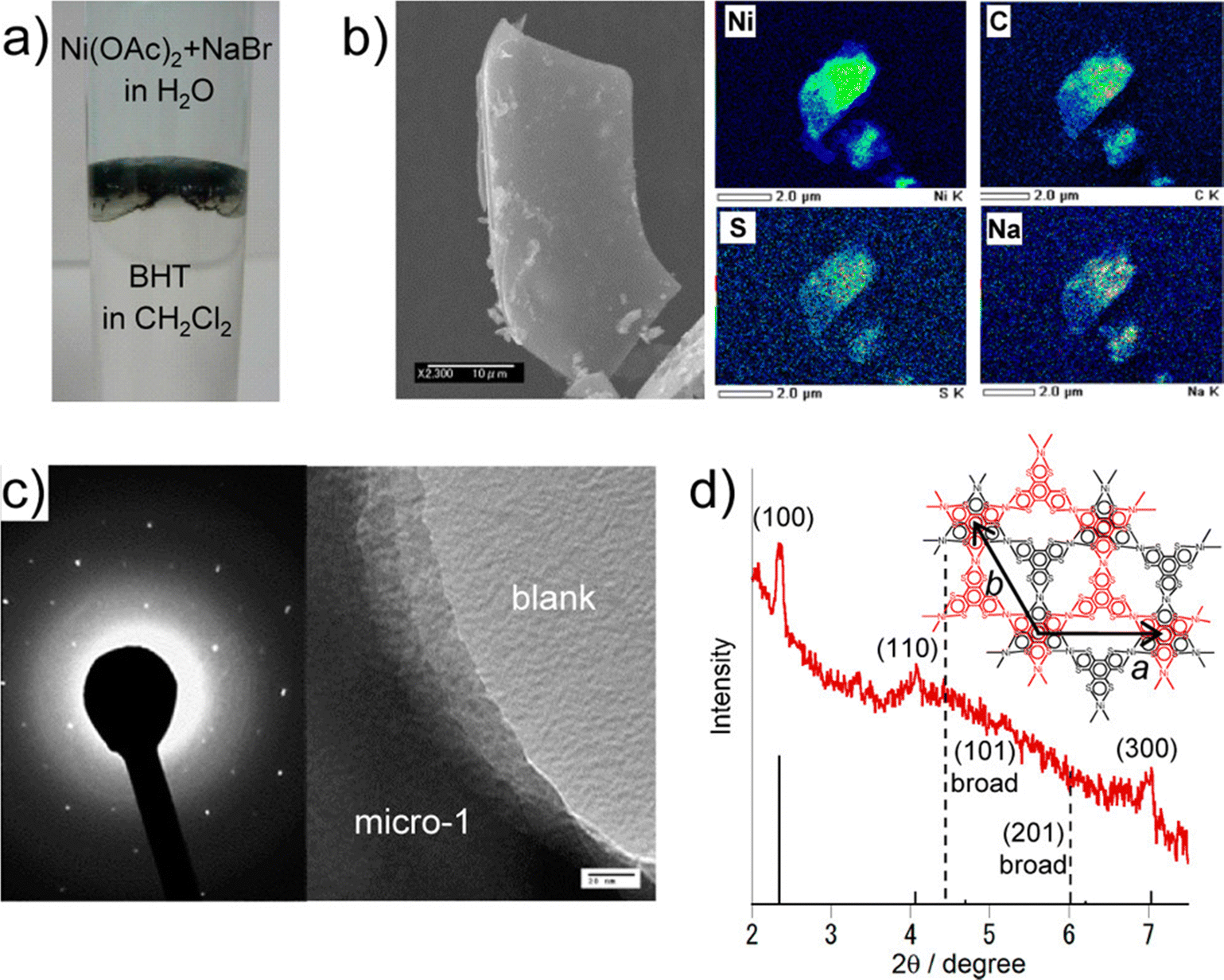 | ||
| Fig. 47 Synthesis and characterization of micro-1. (a) Photograph focusing on the water–CH2Cl2 interface holding micro-1. (b) (left) FE-SEM image and (right) elemental mapping of Ni, S, C, and Na performed using SEM–EDS. (c) (left) SAED pattern and (right) HRTEM image. (d) Experimental (red curve) and simulated (black sticks) XRPD patterns. Reproduced with permission from ref. 241. Copyright 2013, The American Chemical Society. | ||
Bai and co-workers have developed a spray assisted liquid–liquid interface method to prepare a 2D thin film of Cu(BDC) (BDC = 1,4-benzenedicarboxylic acid) MOF by spraying a DMF–acetonitrile solution (1:2) of copper salt on the surface of a DMF–acetonitrile (2:1) solution of H2BDC with a flow rate of 1 μL s−1. The thin film formation was completed after spraying 50 μL. SEM images show that the size of the obtained thin films is ∼200 nm, and the thickness is 0.25–5.55 μm. They have studied the catalytic performance of the thin films for the reduction of 4-nitrophenol to 4-aminophenol.244
3.1.4.2 (b) Gas–liquid interfacial method. In this method, the thin films are synthesized at the gas–liquid interface. In 2013, Kambe and co-workers attempted to synthesize thin films of Ni3(BHT) by a gas–liquid interfacial reaction for the first time.241 They sparged an ethyl acetate solution of benzenehexathiol on the surface (77.5 cm2) of an aqueous solution of Ni(OAc)2 (50 mM) and NaBr (10 mM) using a micro-syringe. The thin film formation was continued for two hours. Scanning probe microscopy (SPM) measurements were used to determine the structure. An AFM study reveals that the thickness of the layer is ∼0.6 nm which is equivalent to the graphene layer on the substrate. The SPM study revealed that the Ni-BHT thin film has a hexagonally ordered monolayer structure.241
In 2013, Makiura et al. synthesized a crystalline, uniform and large-scale thin film of NAFS-13 using a gas–liquid interfacial reaction. In the first step, they spread the molecular building block 15,10,15,20-tetrakis(4-carboxyphenyl)-porphyrinato-palladium(II) (PdTCPP) in ethanol medium on the surface of an aqueous layer and then an aqueous solution of Cu(NO3)2 was slowly injected in the aqueous solution. The chemical reaction between the metal nodes with the carboxylate groups of the PdTCPP building blocks forms a thin layer of the 2D MOF NAFS-13. The slow injection of metal ions makes it feasible to grow the flakes in a microscopic level with a very smooth surface.245
Later, Wu and co-workers developed thin films of semiconductive 2D MOF Ni3(HITP)2 (HATP = 2,3,6,7,10,11-hexaaminotriphenylene) and fabricated an electronic device as a field effect transistor. They observed the formation of thin layers of the 2D MOF on the water surface on heating the aqueous solution of the precursors with trimethylamine to 60 °C. The hydrophobic metal–organic layers float on the water surface. Within 3 min, the film thickness reached 100 nm and the colour of the thin film deepened with increasing thickness to dark violet blue (Fig. 48).246 They have transferred the thin films on SiO2/Si wafer substrates and then patterned Au electrodes are deposited on the top to form the porous FET.
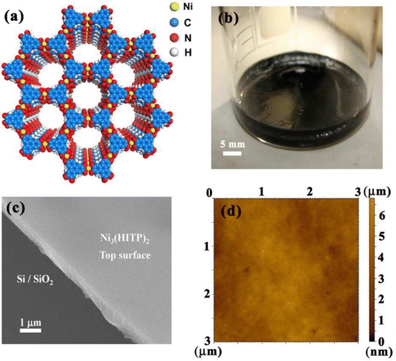 | ||
| Fig. 48 (a) Crystal structure of Ni3(HITP)2. (b) Photograph of a Ni3(HITP)2 membrane formed at the air–liquid interface. (c) SEM and (d) AFM images of the top surface of a Ni3(HITP)2 membrane. Reproduced with permission from ref. 246. Copyright 2017, The American Chemical Society. | ||
3.1.4.3 (c) Langmuir–Blodgett deposition. In 2010, H. Kitagawa and co-workers developed thin films of the 2D MOF NFAS-1 using the Langmuir–Blodgett technique.247 This technique allows the growth of a monolayer at the liquid–air interface and to transfer it easily to a substrate. These authors prepared a chloroform/methanol solution of [Co(TCPP)] (TCPP = 5,10,15,20-tetrakis(4-carboxyphenyl)porphyrin) and pyridine that was spread on CuCl2·2H2O in water medium to form a Langmuir film on the surface. The chemical reaction between CoTCPP and copper leads to the formation of a paddle-wheel-based 2D coordination polymer with the apical positions occupied by pyridyne moieties which allow the 2D layers to assemble by interlayer π⋯π interactions. The 2D metal–organic thin films were then transferred onto Si substrates and stacked by a sequential layer-by-layer growth procedure to form thin films of any desired thickness. Growth of thin films was monitored by absorption and X-ray photoelectron spectroscopy while detailed crystallinity, homogeneity and orientation were studied by XRD analysis. The thickness of the thin film is 20 nm after 20 cycles of deposition on the substrate. θ-Scan shows that the 2D layers are parallel to each other but they are tilted at an angle of 0.3°.247
Kitagawa et al. have also prepared thin films of another 2D MOF: NAFS-2, with a similar method using a non-metalated porphyrin: 5,10,15,20-tetrakis(4-carboxyphenyl)porphyrin (H2TCPP) as a building to form the 2D layered MOF in the absence of pyridine (Fig. 49). The water molecules coordinate to the copper centres within the dinuclear paddle-wheel units. Here, the tilting angle is 3° and the authors suggested that this is due to the absence of stacking interactions between the layers.248
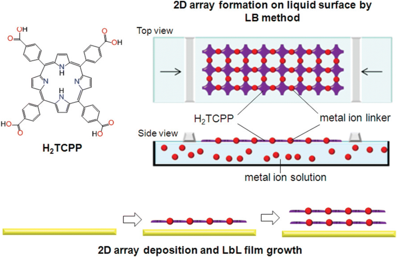 | ||
| Fig. 49 Schematic illustration of the representative assembly processes of NAFS-2 by combined Langmuir–Blodgett/layer-by-layer (LB-LbL) nanofilm growth technique. Reproduced with permission from ref. 248. Copyright 2011, The American Chemical Society. | ||
3.1.5.1 (a) Solvothermal synthesis. In this method, the SAM-functionalized substrates are immersed in a solution of the reactants for the growth of MOF thin films by solvothermal treatment. However, the relatively lower thermal stability of most SAMs on the substrates makes it difficult for practical use.249 In this regard, thermally stable robust alkylsiloxane-based SAMs can be used to functionalize the substrate. Zacher et al. modified SiO2 substrates by reacting them with 10-undecenyltrichlorosilane and oxidizing the ending group to form carboxylic acids which have been further used to form thin films of HKUST-1 and [Zn2(BDC)2(DABCO)] (dabco = 1,4-diazabicyclo[2.2.2]) by directly immersing the SAM functionalized substrate into reactant solutions for solvothermal treatment (Fig. 50).250
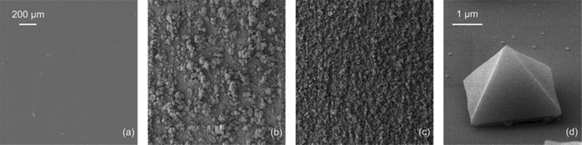 | ||
| Fig. 50 SEM images of [Cu3(btc)2] coatings on (a) bare SiO2, (b) Al2O3 (sapphire) and (c) ALD-Al2O3. (d) Single pyramidal crystal of [Cu3(btc)2] grown on c-plane sapphire. No crystal growth takes place on the SiO2 surface whereas densely packed obviously polycrystalline agglomerated [Cu3(btc)2] microcrystals were formed on sapphire and ALD-Al2O3. Reproduced with permission from ref. 250. Copyright 2007, Royal Society of Chemistry. | ||
3.1.5.2 (b) Crystallization from aged mother solution. In this method, the mother solution, after almost complete crystallization by the solvothermal method, is used for further thin film fabrication with the idea that the solution can form new crystallites. Hermes and co-workers have prepared a thin film of MOF-5 by this method on SAM-functionalized substrates.251
3.1.5.3 (c) Layer by layer (LBL) growth. In this method, as the first step, the substrate is functionalized with SAMs and the ending group of the SAMs is exposed to metal and ligand solutions alternatively. Such external control over the reaction process allows thickness-control of the thin films which is almost impossible for other processes mentioned here.
Shekhah et al. attempted to synthesize thin films of MOF for the first time using this LBL method.252 As the first step, the Au substrate was reacted with 16-mercaptohexadecanoic acid (MHDA) to functionalize the substrate. Then, the SAM-functionalized substrate with carboxylic ending groups was allowed to react with a zinc(II) acetate solution, removed from the solution and washed. Afterwards, it was reacted with a solution of the BTC ligand. XPS, Infrared reflection Absorption Spectroscopy (IRRAS) and Near edge X-ray absorption fine structure spectroscopy (NEXAFS) indicate the absorption of BTC ligands on the surface. When functionalized SAM was reacted with BTC in the absence of Zn(II) ions, there was no absorption of BTC. AFM micrographs show that the thickness of the metal–organic layer is ∼1.6 nm. The thickness of the deposited layer increases with the number of cycles (Fig. 51).252
 | ||
| Fig. 51 (a) Proposed model (front view) for the layer-by-layer growth of the BTC ligand on the MHDA SAM obtained by repeated immersion cycles in solutions of Zn(OAc)2 and BTC. (b) Side view showing that the layers are tilted with respect to the surface normal. For clarity, the model simplifies the assumed structural complexity of the carboxylic acid coordination modes (i.e., mono and bidentate) and the likely presence of additional species such as water molecules at the Zn(II) centre of the MOF layers. Reproduced with permission from ref. 252. Copyright 2007, American Chemical Society. | ||
These authors also formed a thin film of HKUST-1.253 In this case, they functionalized a gold substrate with 16-mercaptohexadecanoic acid (MHDA) and 11-mercaptoundecanol (MUD). The SAM-functionalized substrate with carboxylic groups was reacted sequentially with copper(II) acetate and H3BTC and monitored by in situ surface plasmon resonance (SPR) spectroscopy. Both, the SPR and IR spectral analyses show that the deposition of the HKUST-1 MOF from the sub-monolayer to the multilayer proceeds with a sequential reaction of metal ions and ligands. XRPD data collected for the thin films obtained after 40 cycles of sequential deposition showed the formation of highly crystalline oriented thin films with crystal growth along the [100] direction. These authors also observed that the thin film formation was unsuccessful in the presence of copper(II) nitrate and suggested that the presence of a paddle wheel cluster in copper(II) acetate is a primary requirement for the formation of a HKUST-1 thin film by this process.
 | ||
| Fig. 52 Schematic diagram of synthesized MOF thin films on Ag-NC. Reproduced with permission from ref. 254. Copyright 2017, The American Chemical Society. | ||
Falcaro and co-workers have utilized Cu(OH)2 nanobelts as a sacrificial layer to form thin films of the Cu(BDC) MOF and of the 3D MOF [Cu2(BDC)2(DABCO)]. Initially, they synthesized Cu(OH)2 nanotubes on the surface of Si wafers and observed that the nano-tubes were located perpendicular to the Si-wafer. Then, these nano-tubes were reacted with a saturated ethanolic solution of H2BDC at room temperature. SEM micrographs show that triangular crystals of Cu(BDC) were grown orthogonally to the nano-tubes. Then, they used 2D nano-belts of Cu(OH)2 and similarly reacted with BDC and form 2D layers of Cu-BDC MOF on the surface. Finally, they reacted Cu(OH)2 nano-belts with BDC and DABCO at 60 °C to form thin films of the porous 3D MOF [Cu2(BDC)2(DABCO)]. The formation of thin films was proven by XRD and SEM analyses and the porosity of the thin film of 3D MOF was measured by N2 adsorption analysis.255
3.2 Gas phase processing
In order to avoid solvent interference in the morphology and/or quality of thin films; recently, gas phase thin film fabrication has become a major research focus in conductive MOFs. Gas phase fabrication proceeds through three different steps: (a) vaporization of the metal ions and ligands, (b) transport of the vapours and (c) deposition.256 To date, three different types of gas phase processing have been developed: (i) physical vapour deposition (PVD), (ii) chemical vapour deposition (CVD), and (iii) atomic layer deposition (ALD). These processes are very new in the field of thin film fabrication of MOFs and will require further studies for the development of optimal conditions. | ||
| Fig. 53 Scheme of the steps used for the ZIF-8 film preparation via the femtosecond pulsed-laser-deposition technique. Reproduced with permission from ref. 258. Copyright 2017, The American Chemical Society. | ||
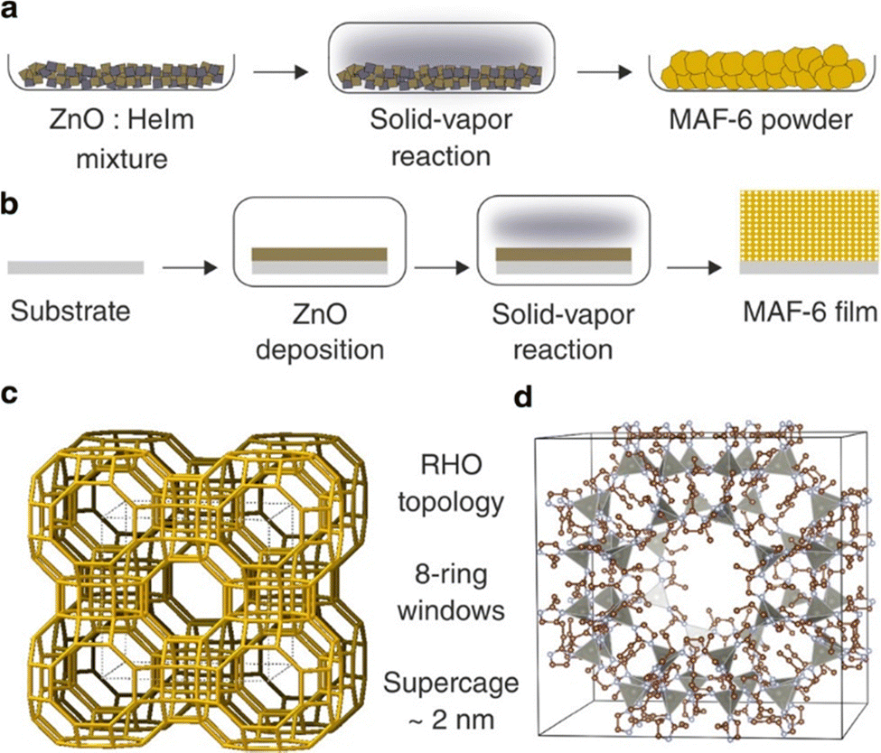 | ||
| Fig. 54 Large-pore MAF-6 from the reaction between ZnO and 2-ethylimidazole vapour. (a) Schematic representation of the CVD powder synthesis. (b) Schematic representation of the film CVD. (c) MAF-6 RHO topology, showing the super-cages connected through octagonal prisms and (d) cubic unit cell of MAF-6. Reproduced with permission from ref. 261. Copyright 2020, The American Chemical Society. | ||
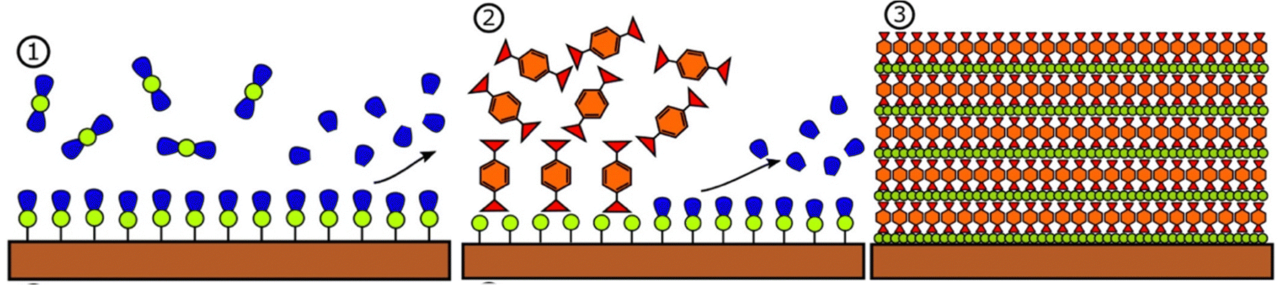 | ||
| Fig. 55 Schematics of the ALD/MLD process for inorganic–organic coordination network thin films, where the process consists of inert-gas-separated pulses of (1) metal (here Ca(thd)2) and (2) organic (here TPA) precursors to yield (3) a monolayer of the hybrid material (here Ca-TP). The film thickness is solely determined by the selected number of repetitions of steps (1) and (2). Reproduced with permission from ref. 265. Copyright 2016, The American Chemical Society. | ||
3.3 Other methods
There are several other methods reported for the synthesis of thin films of MOFs which include seed-assisted growth, sono-chemical, ultrasonic, microwave, electrospray, hot pressing, etc.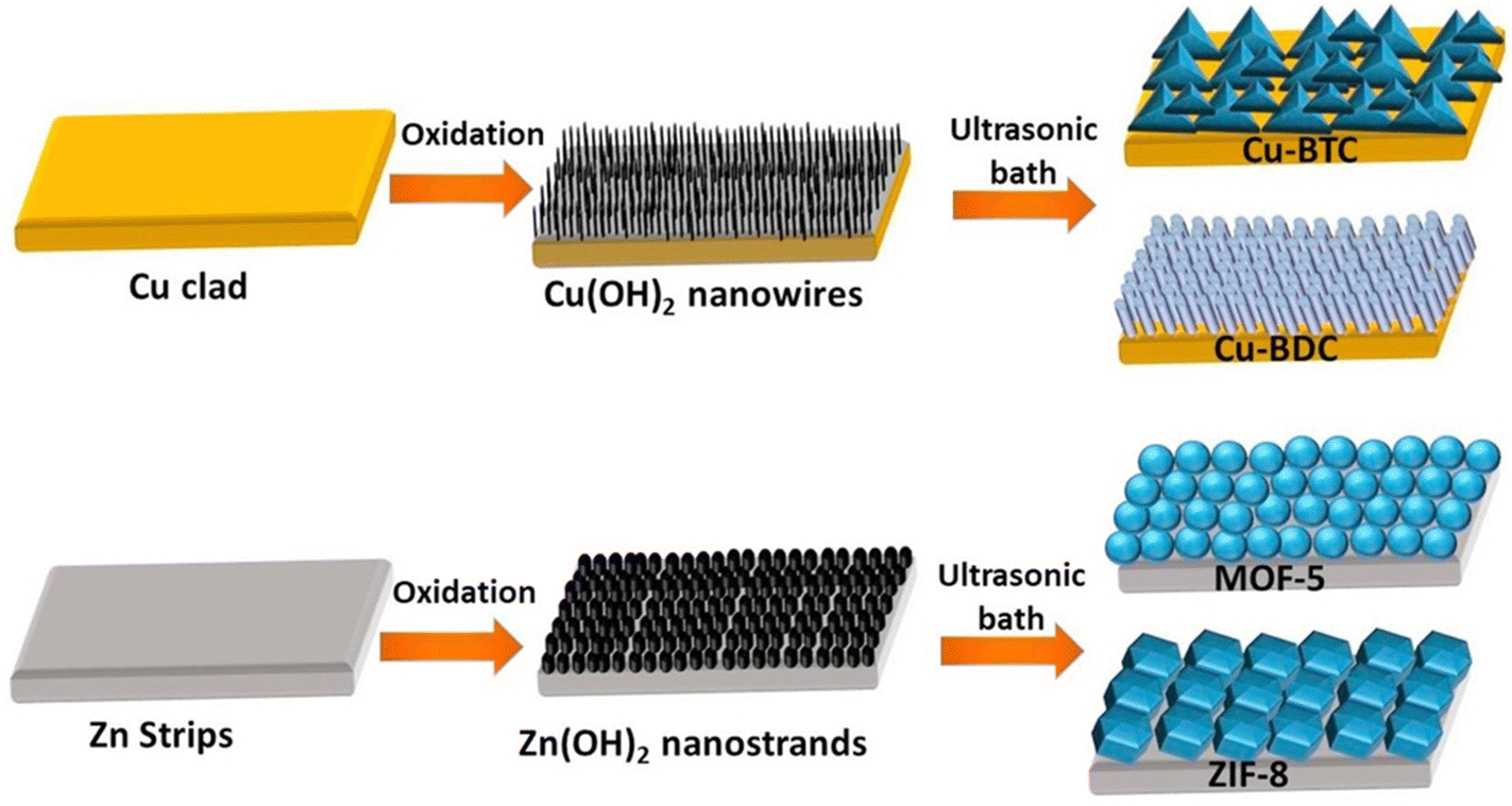 | ||
| Fig. 56 Schematic illustration of the two-step method for the different thin MOF film fabrication. Reproduced with permission from ref. 268. Copyright 2018, Elsevier. | ||
In this case, initially, they oxidized the Cu and Zn metal substrates in the presence of NaOH to form Cu(OH)2 nanotubes and Zn(OH)2 nanostrands after 30 min and 60 min of oxidation, respectively. Then, these oxidized substrates are further reacted with the ligand in an ultrasonic bath with a frequency of 40 kHz and a power of 100 W for different time periods. The temperature of the reaction solution increases with the time of sonication. The synthesized MOF films were further characterized by XRPD, IR and SEM analyses which clearly demonstrate the formation of thin films of the MOFs.
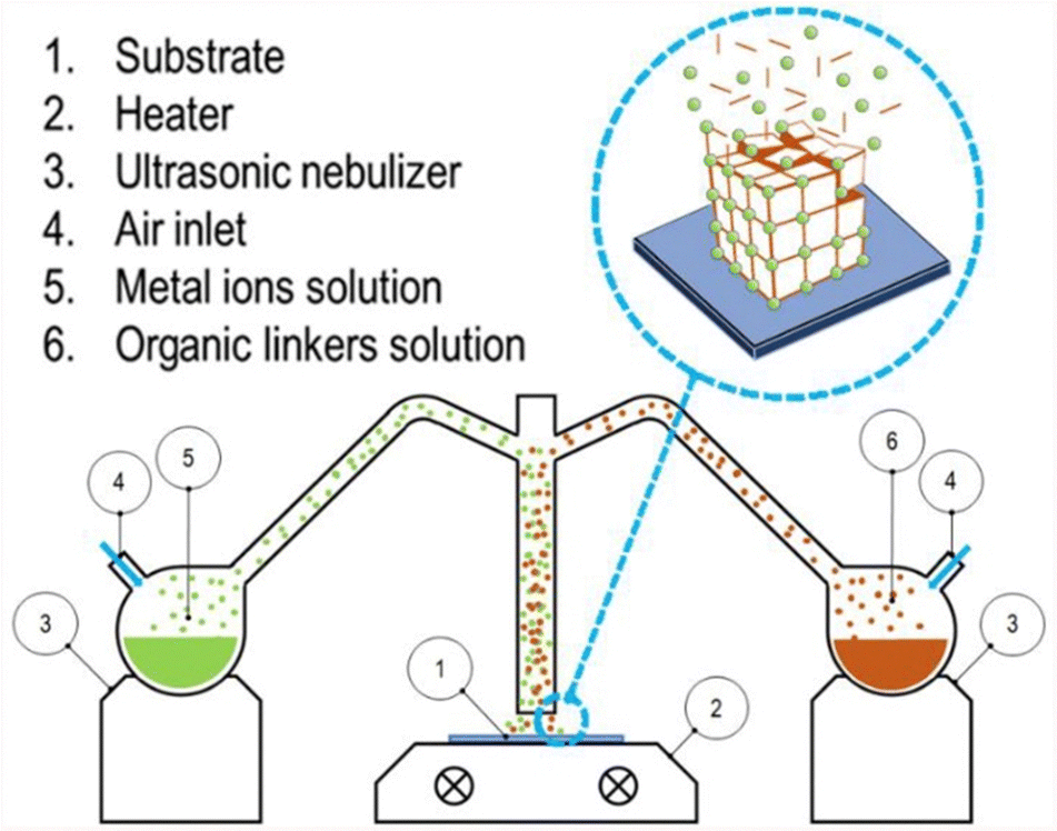 | ||
| Fig. 57 Scheme of the ultrasonic spray deposition system. Reproduced with permission from ref. 269. Copyright 2019, Elsevier. | ||
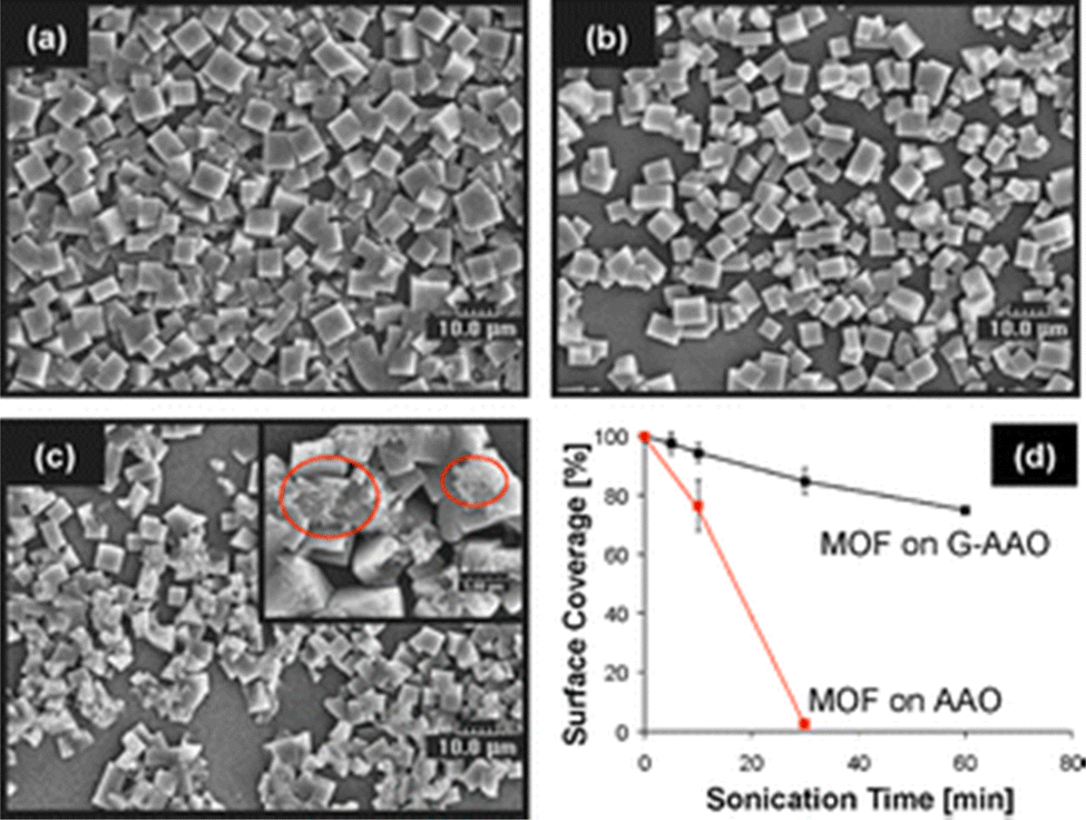 | ||
| Fig. 58 Binding strength of MOF-5 crystals on G-AAO and AAO under sonication: SEM images of MOF-5 films on G-AAO treated under sonication for (a) 0 min (as-prepared), (b) 10 min and (c) 60 min and time-dependent surface coverages (d). The coverage data were obtained by examining the image contrast between MOF crystals and substrates using Adobe Photoshop. The data were normalized to the initial coverages. Reproduced with permission from ref. 270. Copyright 2008, The Royal Society of Chemistry. | ||
 | ||
| Fig. 59 Schematic presentation of the hot-pressing (HoP) method for MOF coating. SBU = secondary building unit. Reproduced with permission from ref. 273. Copyright 2016, The Royal Society of Chemistry. | ||
4. Applications of extrinsically conducting MOFs
Conductive MOFs, at the conjunction of organic semiconductors and inorganic metallic conductors, have aroused much attention as multifunctional materials due to their large surface area, tuneable structure and moderate-to-high charge transport properties. To date, conductive MOFs are used for different applications such as sensing, electrocatalysis, photoconductivity, charge storage, etc. Here, we briefly summarize the applications of ec-MOFs in these relevant fields.4.1 Electrocatalysis
Large surface area and high porosity with an easily accessible large number of transition metal sites with labile exchangeable coordination sites make these conductive MOFs high potential electrocatalysts. Several review articles have covered this topic.30,31,68,274,275 Herein, we only focus on the electrocatalytic applications of guest@MOFs.Dai and co-workers studied the electrochemical HER activity of a MoSx encapsulated UiO-66-NH2 MOF [Zr6(O)4(OH)4(ATP)6] (ATP = 2-aminoterephthalate).281In situ reaction between the MOF ingredients with (NH4)2MoS4 leads to the formation of the MoSx@UiO-66 structure. TEM micrographs clearly demonstrate the formation of NPs of MoSx (with an average size of 0.64 nm) within the UiO-66 nanocrystals of size ∼33 nm. Porosity measurements using N2 adsorption reveal that such encapsulation reduces both the void space and pore diameter which clearly demonstrates the incorporation of MoSx NPs within the void space of the MOF. An IR study shows the presence of p⋯π interaction between the sulphur atoms of the MoSx NPs with the benzene ring of the ligands in the MOF. MoSx@UiO-66 shows excellent HER activity with an onset potential of ∼125 mV and a cathodic current of 10 mA cm−2 at an overpotential of 200 mV with excellent durability (Fig. 60). Theoretical mechanistic analysis reveals that the MoSx NPs act as an electron pool for the reduction of protons on the electrode surface.281
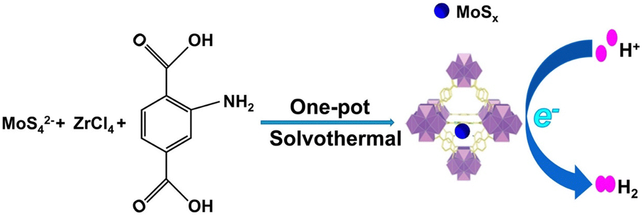 | ||
| Fig. 60 Schematic presentation on the encapsulation of MoSx within the void space of Zr-MOF. Reproduced with permission from ref. 281. Copyright 2016, The American Chemical Society. | ||
In another article, Peng and co-workers have shown the electrochemical HER activity of noble metal nanoparticles (Ru, Ir and Pd) encapsulated MOFs.282 The spontaneous reduction reaction between Ru3+ and the Ni atoms of the Ni-foam produces Ru-NPs and Ni2+, and these Ni2+ ions react with terephthalates to form the MOF architecture. Both SEM and HRTEM micrographs directly demonstrate the formation of Ru-NPs@Ni-MOF, and the ICP study shows that the content or Ru is 2.3% wt; XPS and XAFS analyses identify the presence of interactions between the metal atoms of the NPs with the oxygen atoms of the terephthalate ligands present in the Ni-MOF. Ru-NPs@Ni-MOF shows excellent HER activity with an overpotential of 22 mV to reach 10 mA cm−2 current density in 1 M KOH with very high durability over 24 h. Theoretical calculations reveal that the optimized adsorption-free energy of water and hydrogen due to interfacial bond-induced electron redistribution is responsible for such excellent HER activity.282
Gao and co-workers reported the OER activity of a post-metalated 3D MOF [Th-BPYDC] (BPYDC = [2,2′-bipyridine]-5,5′-dicarboxylate) with metal(II) chlorides. The free bipyridyl groups can react and bind with different metal chlorides (CoCl2, NiCl2 and CuCl2) to encapsulate the metal salts within its architecture. Simulated structural analysis shows that the Co/Ni/Cu metal centres are in 4-coordinated square planar conformation with MN2Cl2 coordination sphere (Fig. 61(a) and (b)). XANES (X-ray absorption near edge structure) spectroscopy reveals the +2 oxidation state of the guest metal ions within the exceptionally stable Th(VI)-BPYDC MOF. The CoCl2@Th-BPYDC MOF structure shows excellent OER activity with an overpotential of 388 mV at 10 mA cm−2 current density in 0.1 M HClO4 electrolyte, which is much lower than NiCl2@Th-BPYDC (482 mV) and CuCl2@Th-BPYDC (646 mV) and comparable to IrO2 (Fig. 61(c) and (d)). This catalyst also shows excellent stability for this electrochemical reaction. Theoretical analysis reveals that during acidic HER, the coordinated chloride atoms rotate and facilitate the binding and activation of the substrate.286
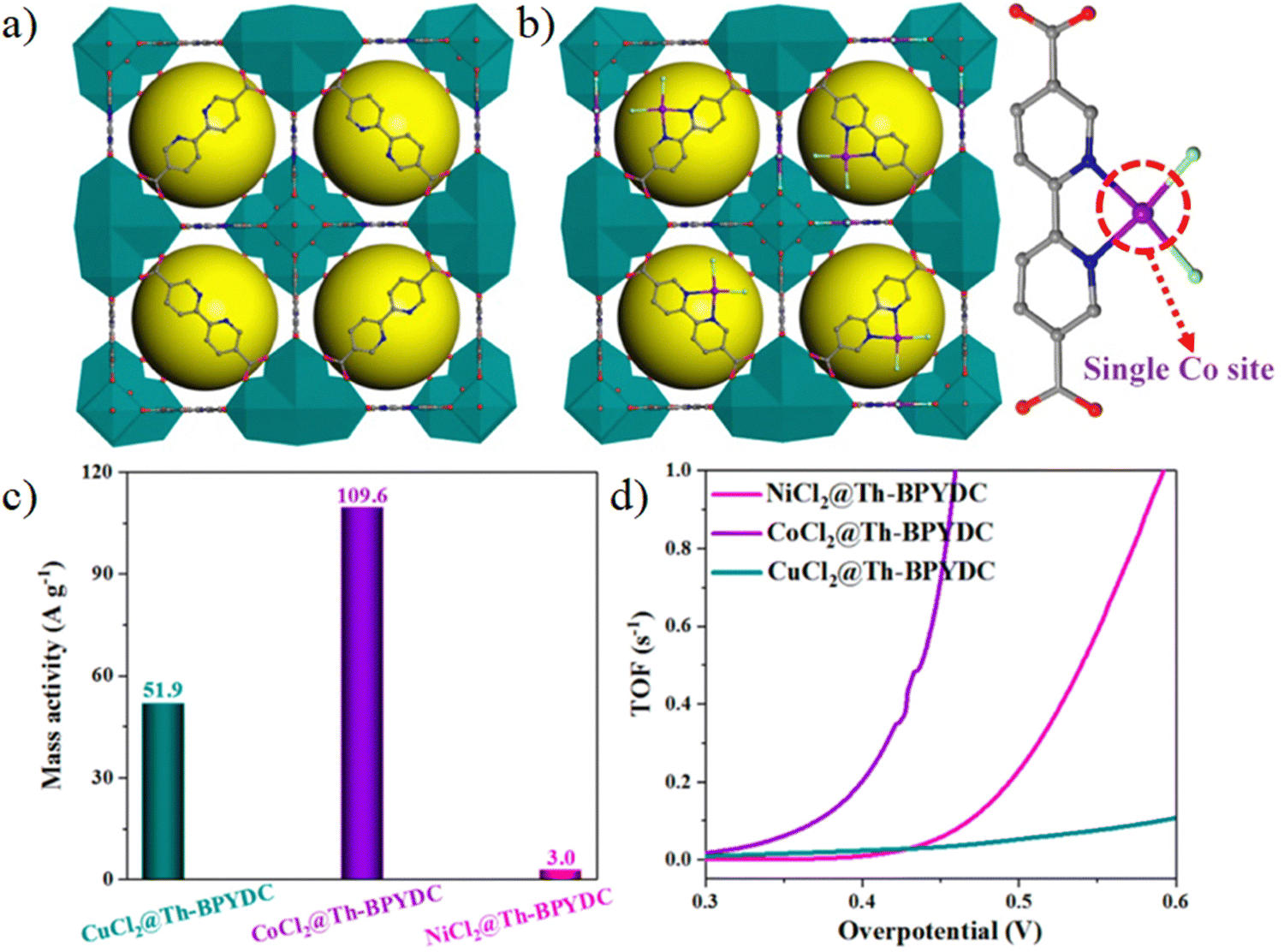 | ||
| Fig. 61 Crystal structure of (a) Th-BPYDC and (b) CoCl2@Th-BPYDC. (c) Mass activities normalized to the metal mass of catalysts (d) TOF plot. Reproduced with permission from ref. 286. Copyright 2016, The American Chemical Society. | ||
In another work, Zhang and co-workers embedded CoFeOx nanoparticles within the 2D layers of a Co–imidazolate framework using an in situ method.287 The formation of CoFeOx nanoparticles within the structure of the Co–Im framework was demonstrated using XRPD, FE-SEM and TEM analyses. These metal-oxide NP-embedded 2D MOFs can be easily exfoliated by ultrasonication while the parent MOF is inert towards ultrasonication. ICP-OES study shows that the amount of Fe within the MOF is 4.14%. An XRPD study reveals that the inter-layer gap between the 2D layers increases during exfoliation and as a result, the porosity also increases from 11.2 m2 g−1 to 98.6 m2 g−1. A TEM study shows that the thickness of the exfoliated 2D layers is about 3 nm. Such metal oxide-embedded 2D MOF has shown excellent OER activity with a very low overpotential of 232 mV at 10 mA cm−2 current density with good stability.287
Luo et al. have shown a significant enhancement of the electrocatalytic OER activity of Ni-HHTP by encapsulation of ferrocene methylamine (Fc-NH2).288 Given the pore diameter of the Ni-HHTP framework, they attempted to encapsulate different types of ferrocene derivatives like Fc, Fc-COOH, Fc-(COOH)2 and Fc-NH2 but successful encapsulation was only achieved for Fc-NH2, through protonation, based on electrostatic host–guest interactions. Several samples were prepared by varying the amount of Fc-NH2 concentration and the reaction time. The encapsulation was characterized using XRPD, HRTEM, XPS and EDXS analyses. The electrocatalytic OER activity reveals that the Fc-NH3+@Ni-HHTP (Fc content ∼0.011 mmol mL−1) shows better electrocatalytic OER activity with an overpotential of 482 mV at 10 mA cm−2.288
Miao and co-workers have reported the ORR activity of Co–salen encapsulated MOF MIL-100(Cr).291 The encapsulation of the cobalt–salen complex was done by a multistep method in which the pre-synthesized MOF particles are dispersed in a solution of cobalt acetate for immobilization of metal ions within the MOF and then reacted with the H2 salen ligand. The encapsulation was monitored by XRPD, IR and UV analyses. N2 adsorption studies reveal that the overall porosity of the parent MOF decreases from 1293 m2 g−1 to 820 m2 g−1 due to encapsulation. This cobalt–salen@MIL-100(Cr) has shown electrocatalytic ORR activity at a potential of −0.21 V at a pH of 6.84. It also shows excellent durability for the four-electron reduction from oxygen to water as evidenced by chrono-coulometry.291
Patra et al. immobilized both laccase and ABTS (2,2′-azino-bis(3-ethylbenzothiazoline-6-sulfonic acid)) within the MIL-100(Fe). This material also shows electrocatalytic ORR activity with high current density and excellent stability over a long period.292
Cho et al. modified Cu-BTC MOF with CuS-NPs both on the surface and in the void space. Several samples were prepared by varying the amount of CuS. The presence of CuS within and on the Cu-BTC MOF particles enhances its electrical conductivity over 109 times. The CuS@Cu-BTC MOF (28% wt) shows significant electrocatalytic ORR activity with an onset potential of 0.91 V and a kinetic current density of 11.3 mA cm−2 at 0.55 V vs. RHE via a four electron reduction pathway.293 In another article, Si et al. encapsulated Pt-NPs within the porous conducting [Ni3(HITP)2] framework and the obtained Pt@[Ni3(HITP)2] shows excellent ORR activity.294
Kung and co-workers have studied the electrochemical CO2 reduction capacity of CuNPs-loaded MOF NU-1000.299 Thin films of the MOF were prepared by soaking FTO-coated glass substrates within the reagents via a solvothermal method (Fig. 62). The obtained thin films were further soaked in a solution of Cu(dmap) (dmap = dimethylamino-2-propoxide) to incorporate them within the void space of the MOF and were then reduced with hydrogen gas. Such encapsulation changes the colour of the films to green and reduces the porosity substantially. ICP-OES indicates that 4.0 Cu atoms are deposited per Zr6 unit of the MOF and they are located between each Zr6 cluster of the framework. The CuNP-loaded NU-1000 MOF shows electrochemical CO2 reduction to CO with an onset potential of −0.82 V with a faradaic efficiency (FE) of ∼31%.299
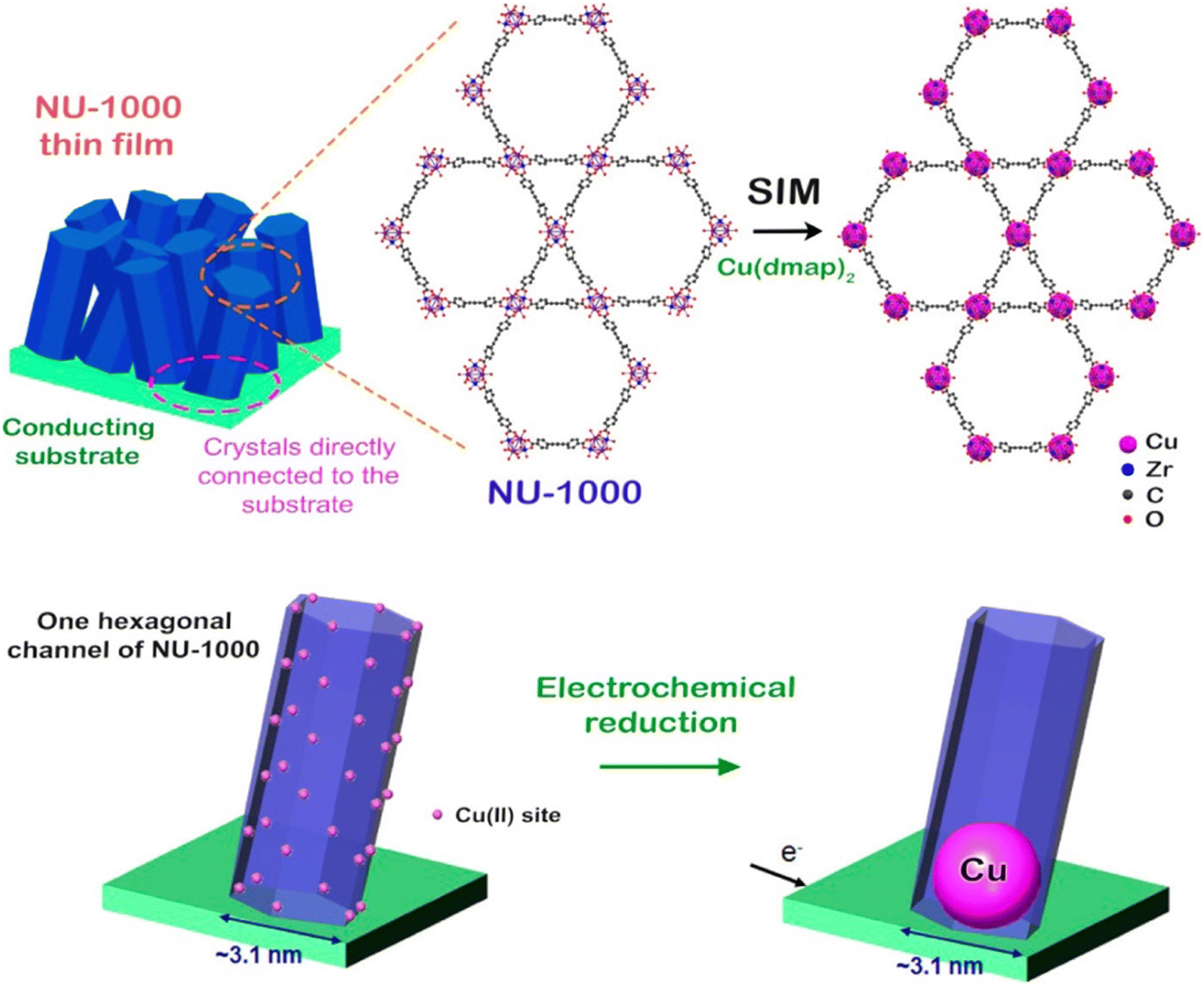 | ||
| Fig. 62 Schematic representation of the solvothermal deposition in MOF (SIM) to install single-site Cu(II) into the NU-1000 thin film and the electrochemical reduction of Cu(II) to generate metallic Cu nanoparticles. For simplicity, hydrogen atoms are not shown in the structure. Reproduced with permission from ref. 299. Copyright 2017, The American Chemical Society. | ||
Yan et al. reported the enhancement of electrochemical CO2 reduction to ethylene by encapsulation of metal-porphyrins (M-TCPP where M = Fe, Co and Ni; and TCPP = tetrakis(4-carboxyphenyl)porphyrin) within HKUST-1.300 The successful one-step encapsulation was characterized by XRPD, IR, SEM, TEM, XPS and elemental analyses. The electrochemical CO2 reduction by HKUST-1 results in the production of ethylene with FE of 16.85% at a potential of −1.27 V while for the Fe-TCPP@HKUST-1 the FE is 33.42% at a potential of −1.17 V. The other two materials Ni-TCPP@HKUST-1 and Co-TCPP@HKUST-1 show almost similar activity as the Fe-TCPP-encapsulated MOF. These authors proposed that the encapsulated M-TCPP moieties supply the intermediate CO towards the Cu-centres of HKUST-1 to promote C–C coupling for ethylene production.300
In another article, Xin and co-workers have shown the electrocatalytic CO2 reduction by a polypyrrole-loaded MOF-545-Co. PPy@MOF-545-Co shows a large current density of 32 mA cm−2 at −1.1 V, a much higher current density than that of PPy@MOF-545 and MOF-545-Co. The faradaic efficiency for CO production is 98% at −0.8 V. These authors propose that the PPy moieties within the MOF facilitate the electron transfer during CO2 reduction.301


Cyclic voltammetry was used by Wang and co-workers for the electrochemical oxidation of acetaminophen (AP) by a Au-NP-loaded ZIF-L.306 Au-NP@ZIF-L/GCE shows an increase in oxidation current compared to bare GCE and ZIF-L/GCE. The synergy between high electrical conductivity and porosity of ZIF is the main driving force for such oxidation. AuNP@ZIF provides a favourable environment for transferring species in solution and is beneficial for accelerating electron transfer between the electrode and AP. The oxidation peak current also increases with increasing the scan rate, suggesting a diffusion-controlled process. The oxidation peak shifts to negative values with increasing pH which clearly indicates that protons take part in the electrochemical oxidation of AP.306
4.2 Electronic sensing
Electronic sensors are analytical devices that show the presence of a particular analyte or their existence above a certain concentration by transducing different electronic parameters like resistivity, capacitance, etc.307 Several important parameters like technical simplicity, easy fabrication, cost-effectiveness, sensitivity and selectivity make these electronic sensors highly attractive in analytical research.308 The chemical tuneability of MOFs provides an enormous opportunity to tune the electrochemical performance and recognition behaviour of the fabricated devices. The inherent void space can also accommodate different analytes, and the large surface area of MOFs facilitates their interaction with the metal centres or with the organic building blocks. Again, the easy fabrication of MOF thin films in electronic devices also boosts their application in sensing devices.309 To date, different methods like chemiresistive, chemicapacitive, impedance, Kelvin probe, FET, etc. have been adopted for this purpose.310–312 A number of MOFs and MOF composites with other conducting substances have been developed for sensing various types of analytes: gases, ions, toxic molecules and biomolecules. Several reviews have already been published on this topic which include either pristine MOF or MOF composite as the sensing electronic platform but there is no review that highlights the sensing properties of extrinsically conducting MOFs. Here, we discuss some sensing behaviour of extrinsically conducting MOFs by classifying analytes into different categories.Shiozawa et al. have shown the chemiresistive sensing of Ar by TCNQ-doped Co-MOF-74. Co-MOF is insulating in nature and the encapsulation of TCNQ increases its conductivity. This porous TCNQ@MOF-74 shows Ar absorption behaviour and a decrease of the resistance of the framework with increasing the amount of Ar.313 Kim and co-workers reported the highly selective sensing of NO2 by Pt@Cu3(HHTP)2 MOF thin-film.314 Also Koo et al. developed Pt@Cu3(HHTP)2 and Pd@Cu3(HHTP)2 for NO2 sensing.315
Zheng and co-workers developed thin films of [Cu3(HHTP)2] by the vapour phase layer-by-layer method. The obtained thin films were used for the detection of H2 and NH3.316 Very recently, Lim et al. have developed nanoparticles of HKUST-1 on Laser-Induced Graphene (LIG) sheets. The obtained HKUST-1@LIG has shown chemresistive sensing towards NO2.317
Vilian et al. have shown electrochemical nitrite ion detection by PdNPs@MIL-101(Cr) due to the electro-oxidation of nitrite ions. In the presence of nitrite ions, the CV of the electrochemical device shows an irreversible anodic peak at 0.904 V with a peak current of 120 nA which indicates the oxidation of nitrite. Under optimal conditions, the oxidation current increases linearly with increasing nitrite concentration from 5 to 150 nM and the detection limit is 1.3 nM. A pH-dependent electrocatalytic study also reveals that pH = 7 is the most suitable condition for electro-oxidation. The peak current also increases with the scan rate in the range of 0.01–0.1 V s−1 and the anodic peak potential shifts to more positive values. These authors have further used PdNPs@MIL-101(Cr) for nitrite ion detection in sausage and pickle samples.102
Bhardwaj et al. have studied the conductometric detection of prostate cancer antigen by TCNQ-doped HKUST-1 MOF. The slow diffusion of TCNQ into the pores of HKUST-1 MOF increases its electrical conductivity from 10−14 S cm−1 to 7.3 × 10⁻⁴ S cm−1. The physical absorption of antibodies on the surface of TCNQ@HKUST-1 leads to the decrease of conductance of the thin film by a factor of almost three (2.7 × 10⁻⁵ S cm−1). The antibody-decorated TCNQ-doped HKUSTE-1 thin film was used to detect antigens in the concentration range of 0.01–150 ng mL−1. With increasing concentration of PSA (prostate cancer antigen), the electrical conductivity of the device decreases which is attributed to the antibody–antigen interaction.318 Selvam et al. developed a composite material by mixing SeS2@Co-MOF with Au@PANI. The material was used for electroanalytical sensing of patulin mycotoxin.319 In another article, Ma et al. reported the electrochemical glucose (Glu) sensing by Cu@Co-MOF with rapid current response, low interferences and high stability and repeatability to Glu detection.320
4.3 Charge storage
Electrochemical energy storage has gained much interest in the field of conducting porous MOFs for their high charge storage densities, fast charging processes, large number of cycles and large surface areas.321,322Kung and co-workers have shown the pseudo-capacitance behaviour of NiCB@NU-1000 MOF (CB = bis(dicarbollide)). Redox behaviour of thin films of NU-1000, NiCB@NU-1000, manganese oxide deposited by atomic layer deposition in MOF (AIM) on NU-1000 (Mn-AIM@NU-1000) and Mn-AIM-NiCB@NU-1000 was explored using cyclic voltammetry. The initial three samples show negligible charge storage behaviour while the specific conductance value of Mn-AIM-NiCB@NU-1000 is 270 F gMnO2−1.169
Wang and co-workers have encapsulated polypyrrole (Ppy) within the pores of the Keggin polyoxometalate PMo12O403− (PMo12)-based MOFs, NENU-5. The composite of NENU-5 with Ppy shows a high specific capacitance (5147 mF cm−2) larger than pure NENU-5 MOF. These authors prepared a symmetric supercapacitor with PPy@NENU-5 that shows an aerial capacitance of 1879 mF cm−2.323 Liu and co-workers have used the same NENU-5 to prepare a composite with PPy to study the charge storage property.324 In another report, Wei and co-workers have developed another composite of PMo12V2-encapsulated MOF HKUST-1 with reduced graphene oxide to study the charge storage properties. This composite shows a reversible capacity of 1075 mAh g−1 and a capacity retention of nearly 100% at both 2000 and 3000 mA g−1 for over 400 cycles.325
Shao and co-workers have reported a large charge storage capacity of PANI@UiO-66. The CV study shows that the current density increases with the scan rate and a maximum specific conductance value of 1084 F g−1 is obtained at a current density of 0.5 A g−1. This PANI@UiO-66 MOF showed 84% of capacitance retention after 3500 galvanostatic charge–discharge (GCD) cycles. They also developed an advanced flexible solid-state supercapacitor device with PANI@UiO-66. This flexible symmetric supercapacitor shows a large specific capacitance of 886 F g−1 at a current density of 0.5 A g−1. The framework also shows high stability with 91% retention of specific capacitance after 5000 GCD cycles.195
Ferhi and co-workers reported the charge storage capacity of another polyaniline-encapsulated MOF. They have observed that PANI@d-MOF-808 (defective zirconium MOF 808) with a polymer:MOF ratio of 60:1 shows the maximum capacitance behaviour (Fig. 63). The highest specific capacitance value obtained is 188 F g−1 at 30 mV s−1 in 1 M KOH with ∼100% retention of capacitance after 10000 cycles.326
 | ||
| Fig. 63 Synthetic route to prepare MOF-808, d-MOF-808 and d-MOF-808@PANI-15:1, 30:1, and 60:1. Reproduced with permission from ref. 326. Copyright 2017, The American Chemical Society. | ||
Zheng and co-workers have shown the electrochemical capacitance behaviour of Cu2+1@Cu-MOF/Cu-foam.327 They prepared Cu2+1@Cu-MOF by a two-step method: in the first step, Cu(OH)2 nano-rods were grown on the surface of copper foam and in the second step, these nano-rods were reacted with p-phthalic acid at 350 °C. At high temperatures, these Cu(OH)2 nano-rods are reduced to Cu2+1O while some of them react with p-phthalic acid to form Cu-MOF. The obtained Cu2+1O@Cu-MOF shows an enhanced capacitance value (∼2.5 F cm−2 at 2.0 mA cm−2) compared to Cu(OH)2/Cu-foam and Cu2+1/Cu-foam (∼0.8 and ∼0.9 F cm−2 at 2.0 mA cm−2, respectively). This supercapacitor shows a high energy density of 38.3 W h kg−1 at a power density of 824.6 W kg−1 with 90% capacitance retention after 5000 cycles.327
In another report, Wang et al. have shown a very high capacitance value of 1197 F g−1 at a current density of 1 A g−1 of PANI@MIL-101 with good cyclic stability of 81% retention even after 10000 cycles.94
Recently, Tsai et al. have shown a significant enhancement of the charge storage capacity of the 2D MOF Zr-BTB (where BTB = 1,3,5-tri(4-carboxyphenyl)-benzene) through encapsulation of PANI.328 They used a sulfonate-based ligand to spatially separate the polymeric chains of PANI thanks to the electrostatic interaction between the aniline unit and the negatively charged sulfonate groups. Initially, they grafted the sulfonate-based ligand on the metal nodes of 2D Zr-BTB-SO3. Afterward, PANI was encapsulated through in situ polymerization. The resulting PANI@MOF shows a specific capacitance of 515 F g−1 at a charge–discharge current of 0.5 mA cm−2, which is much higher than those achieved by the pristine PANI (230 F g−1), PANI@ZrBTB (137 F g−1) and the physical mixture of PANI and ZrBTB-SO3 (130 F g−1).328
4.4 Photo-conductivity
Photoconductivity is a useful property for applications such as solar cells, photo-electrocatalysis etc. In a photoconductive material, upon light excitation, electrons will jump from the valence band to the conduction band by creating holes in the valence band. In order to develop a photoconductive MOF, a donor–acceptor pair is required.203 So, to design an extrinsically photo-conducting MOF, a donor–acceptor pair should be formed within a host MOF. There are two different possibilities: either the MOF acts as a donor and the guest as an acceptor or vice versa. Liu and co-workers have studied the photoconductivity of thin films of three different MOFs upon C60 encapsulation.152 They have prepared thin films of C60@Cu-BPDC (BPDC = biphenyl-dicarboxylate), C60@ZnTPP (TPP = 5,15-bis-(3,4,5-trimethoxyphenyl)-10,20-bis(4-carboxyphenyl)porphyrine) and C60@ZnDAP (DAP = 10,20-bis(4-carboxyphenyl)-5,15-diazaporphyrine) with the LBL technique. Two-probe conductivity measurements show that Cu-BPDC (2 × 10⁻¹³ Sm−1) shows an enhancement of 4 orders of magnitude due to encapsulation of C60. However, the enhancement of conductivity is less than 10% for C60@Cu-BPDC upon illumination. C60@ZnTPP shows a conductivity value of ∼1.5 × 10⁻¹¹ S cm−1 while the parent MOF has a conductivity value of 1.5 × 10⁻¹³ S cm−1 and the conductivity value rises by 100 times upon illumination with light of 455 nm (Fig. 64). | ||
| Fig. 64 (a) The structure of C60@Zn(TPP). O = red, Zn = dark grey, N = blue and H = white. For clarity, C in the MOF scaffold is shown in cyan, and C of fullerene is grey. (b) The DC current I at a voltage of 2 V is measured while the sample is irradiated with light of 640 nm, 530 nm, 455 nm, 400 nm and 365 nm wavelength. The current without light irradiation is 0.11 nA. Reproduced with permission from ref. 152. Copyright 2019, Wiley & VCH. | ||
This difference is obviously due to the cooperative charge transfer between the donor porphyrin and the acceptor C60 moieties. The related MOF C60@ZnDAP also shows a 100 times enhancement of the electrical conductivity upon excitation with 455 nm wavelength. This different photoelectric behaviour of these porphyrin-based MOFs is due to their different electronic structure. In order to explain the photoconductive behaviour of these MOFs, these authors have performed quantum mechanical calculations which reveal that the LUMO of TPP is lower in energy than in the C60@ZnTPP MOF and this facilitates both the direct and photo-induced electron transfers between porphyrin and C60. Upon excitation, the Soret band of the porphyrin was activated to generate electron–hole pairs and promote their transfer by hampering their recombination and electron back transfer. Han and co-workers have shown the photoconductive behaviour of AgNC@Rb-CD-MOF. AgNC@MOF shows 104 times enhancement of the electrical conductivity upon illumination to reach 2.15 × 10⁻⁷ S cm−1.73 They have established that direct optical excitation and an indirect thermal excitation contribute to the overall enhancement of the electrical conductivity upon illumination and also proposed a tunnelling mechanism for charge transport. Hu et al. have shown the photoconductive behaviour of the MOF [Tb(Cu4I4)(INA)3(DMF)] after iodine adsorption.124 Upon illumination with a Xe lamp, the photocurrent increases from 3.8 to 5.8 μA.
Some of these guest-encapsulated photoconductive MOFs may also be used for photovoltaic cells to convert solar light into electricity. Lee et al. have shown the photovoltaic activity of thin films of two different MOFs, Co-BDC (H2BDC = 1,4-benzene dicarboxylic acid) and Co-NDC (NDC = 2,6-naphthalenedicarboxylate).122 Thin films of these MOFs are prepared via layer-by-layer and iodine was loaded by soaking the thin films within an iodine saturated acetonitrile solution. Absorption spectroscopy confirms the encapsulation of iodine as well as oxidation of Co2+ to Co3+. Such iodine encapsulation converts these two insulating MOFs to semiconductors. Co-NDC shows better conductivity than Co-BDC due to the encapsulation of a larger number of iodine molecules. Both iodine-doped MOFs are used as light-harvesting sensitizers in a TiO2-based photovoltaic cell. The Co-NDC MOF has a power conversion efficiency of 1.12%.122 In another article, Zhang and co-workers reported the solar cell activity of a polyoxometalate-encapsulated MOF.325 The MOF [Fe(BDC)(4,4′-bpy)] was used to encapsulate H3PW12O40 Keggin POMs inside the MOF. This MOF shows an optical response with λmax ∼ 750 nm. The photovoltaic performance of the POM@MOF modified ZnO photoanode shows better performance than bare ZnO. The power conversion efficiency is ∼0.073%.
4.5 Photocatalysis
Some of the conducting MOFs are also used for photocatalytic applications like CO2 reduction, water splitting etc. Yuan et al. have studied the photocatalytic CO2 reduction behaviour of PPy-loaded ZIF-67.334 Due to high electrical conductivity, high aqueous stability and large surface area, PPy@ZIF-67 is used as a co-catalyst for CO2 reduction under visible light in the presence of [Ru(bpy)3]2+ as a photosensitizer. Under these catalytic reaction conditions, PPy@ZIF-67 produces CO and H2 with a CO selectivity of 63%. The encapsulated PPy acts as an electron harvester and transporter for the photogenerated electron from the photosensitizer to the metal nodes. Upon excitation at 500 nm, [Ru(bpy)3]2+ shows the characteristic emission peak at 606 nm, which is quenched by the presence of the co-catalyst PPy@ZIF-67. The weak interactions between PPy and [Ru(bpy)3]2+ enable a more efficient electron transfer within the MOF.334In another article, Fang et al. have shown a similar photocatalytic CO2 reduction of PPy@Al-PMOF-Cu. Porphyrin moieties with Al-PMOF were post-metalated with copper and then pyrrole monomers were encapsulated within the void space. Oxidative polymerization to form PPy was done within the void space and confirmed by TEM, XRPD and IR studies. Such encapsulation of PPy reduces porosity but enhances electrical conductivity. Photocatalytic CO2 reduction to CO (90 μmol g−1 h−1) was obtained by using triethanolamine as the sacrificial agent under visible light irradiation. The porphyrin moiety acts as a photosensitizer, PPy as an electron transporter and the Cu sites as the catalytic active centres.193
4.6 Other applications
Xu et al. have shown thermoelectric properties of PANI-loaded MOFs by measuring the temperature dependence of their Seebeck coefficients.197 The Seebeck coefficients for all the PANI-loaded MOFs (PANI@Co-MOF, PANI@Co-MOF-Br and PANI@Co-Ag-MOF) increase with temperature and all show a p-type thermoelectric behaviour. PANI@Co-MOF-Br has the highest Seebeck coefficient (66.5 μV K−1 at 400 K), much higher than PANI@Co-MOF (46.3 μV K−1) and PANI@Co-Ag-MOF (59.5 μV K−1). They have observed that this trend is different from the electrical conductivity of MOFs due to the coupling effect and the mobility and carrier concentration.197 Jiao and co-workers have reported the electromagnetic absorption (EMA) of PPy@ZIF by evaluating the reflection loss (RL) value. They have observed that the electromagnetic absorption is also dependent on the electrical conductivity of the samples. The higher the electrical conductivity, the higher the absorbance. Pure ZIFs have low EMA performance but it improves with the introduction of PPy within the channels. PZ-3 containing 5% of PPy shows the maximum EMA performance and this can also be tuned by the sample thickness and the frequency of the electromagnetic radiation. The maximum EMA performance for PZ-3 is −49 dB with a sample thickness of 2.9 nm.191 Prasoon and co-workers have shown a diode-like behaviour of thin films of TCNQ-doped Cu-BTEC MOF with a rectification ratio of ∼105.335 Liu and co-workers have shown the photothermal energy storage behaviour of PPy composite with ODA@Cr-MIL-101-NH2 (ODA = 1-octadecanol). The photothermal conversion and storage efficiency of ODA@MOF/PPy-6% reaches values as high as 88.3%.3365. Summary and outlook
During the last two decades, MOFs have become a major research topic thanks to their interesting properties such as ultrahigh surface area, tuneable structure, gas and solvent sorption, size-selective heterogeneous catalysis, sensing, etc. The development of intrinsically conductive MOFs for multiple applications combining electronic properties and structure-based functionalities is hindered by the limited choice of electroactive organic ligands and metal ions to construct these MOFs. In this scenario, the encapsulation of electroactive guest species within the void space of MOFs has gained much attention due to the endless possibilities of guest species and host–guest interactions. A large number of electroactive species can be used as guests to design ec-MOFs by generating mobile charge carriers, host–guest charge transfer interactions or individual conductive pathways. Although significant progress has been made in this field, there are still several limitations such as device fabrication, stability, mechanical properties, etc. In conducting MOFs, the formation of efficient charge transport pathways is the main requisite for the development of highly conductive materials. Based on this conducting pathway, MOFs and PCPs can be classified into two categories: intrinsically (ic-MOFs) and extrinsically conducting MOFs (ic-MOFs). The main differences between both types of conducting MOFs can be grouped in different aspects as (i) design, (ii) synthesis, (iii) structural studies and (iv) conductivity studies.(i) Design: in ic-MOFs, the charge transport depends on the metal–ligand backbone of the framework. Different strategies have been adopted to design ic-MOFs including metal–ligand overlap (use of soft donor-based ligands), redox hopping (use of mixed-valence metal ions), extended organic conjugation (use of highly conjugated ligands) and redox-active radical-based ligands. Thus, the design of ic-MOFs is critically dependent on the metal ions and ligands. However, the limited choice of electroactive ligands, compared to general MOFs, strongly reduces the design possibilities.
In contrast, in ec-MOFs, the charge transport depends on the guest and host–guest interactions. The guests can conduct electrons on their own (as organic conducting polymers) within the void space of the host MOF. In other cases, host–guest interactions create new charge transport pathways within the guest@MOF structure through π-interaction, redox hopping, metal–guest interactions, etc. Here, the large number of possible guests and host–guest interactions provide almost infinite opportunities to design ec-MOFs.
(ii) Synthesis: ic-MOFs are generally synthesized by in situ methods through direct mixing of the chemical components under solvo- or hydrothermal conditions by self-assembly of organic ligands and metal ions. Additionally, some post-synthetic modification can be done by metal ions or organic ligands exchange while keeping the basic MOF architecture.
In contrast, ec-MOFs are very rarely obtained by in situ methods. In most cases, the guest encapsulation is done via the post-synthetic methods. The encapsulated guest species remain either in the void space or grafted to the metal ions or to the ligands. Such post-synthetic encapsulation leads to the non-homogeneous distribution of guests within the host structure. So, the synthesis of ec-MOF is somewhat a bigger challenge compared to ic-MOFs.
(iii) Structural analysis. For the intrinsically conducting frameworks, the detailed structural information enables the rational development of such materials by simply using mixed-valence metal ions, conjugated ligands with an adequate metal–ligand overlap, etc. In contrast, for extrinsically conducting materials, there is little crystallographic evidence of the host–guest interactions and their contributions to the charge transport phenomena of the resultant host–guest materials. However this host–guest interaction has already shown a high potential to enhance the electrical conductivity by several orders of magnitude. Unfortunately, in most cases, the inclusion of guests within the regular confinement spaces of the frameworks reduces the crystallinity of the host and precludes the single crystal X-ray structure determination.
(iv) Conductivity studies. The electrical conductivity of MOFs is measured either on single crystals or on microcrystalline powders. Single crystals of ec-MOFs are very rare as the post-synthetic encapsulation of guest species within the pores of MOFs reduces the single crystalline nature. Therefore, the electrical conductivity of ec-MOFs is measured mostly on pressed pellets or thin films. In the case of ic-MOFs, there are more reports on single-crystal electrical conductivity measurement. The electrical conductivity measurement using pressed pellets or thin films of MOFs is less reliable than single crystal measurements due to the influence of grain-boundary effects. Although for real-world applications, devices can be prepared by using MOF thin films, in order to get a deep understanding of the structure-properties relationships, we need accurate structural and electrical studies.
The maximum electrical conductivity reported to date for ic-MOFs is 1580 S cm−1 for the MOF Cu-BHT (BHT = benzenehexathiolate), measured on thin films by D. Zhu et al.242 whereas the maximum electrical conductivity reported to date for an ec-MOF is 250 S cm−1, measured on single crystals of a BEDT-TTF donor–acceptor charge-transfer based MOF reported by Coronado, Gómez-García et al.137
In this review, we have focused on these guest-containing extrinsically conducting materials. We have classified the guests into three categories: (a) metal-based guest, (b) molecule-based guest and (c) organic conducting polymers. For the reported examples, we have discussed: (i) the guest loading process within the pores/channels of the MOFs and PCPs, (ii) the structural modifications after guest loading (when data is available), (iii) the (most times huge) change in the electrical conductivity and (iv) the charge transport pathway and mechanisms proposed. The review of these extrinsically conducting MOFs shows the following conclusions:
(a) Metal-based dopants: the dopants (metal ions, metal nanoclusters and metal oxides) are incorporated into the MOFs via post-synthetic techniques. The incorporation of metal ions can be done by simple intercalation. This method usually maintains the crystallinity and allows the study of the crystal structure of the intercalated material. Structural studies show that the metal ions are mainly located around the ligand donor sites of the framework and, accordingly, the electrical conductivity is obtained thanks to a charge transport hopping mechanism. The metal nanoclusters (MNCs) are usually loaded by intercalation of metal ions followed by a reduction to form metal nanoparticles. The reduction can be done by either incorporating a secondary reducing agent or by the MOF itself, although this chemical reaction decreases the crystalline nature of the frameworks. The enhancement of the electrical conductivity is due to the easy charge transport through the MNCs within the MNC@MOFs by the hopping mechanism. Metal-oxide encapsulated within MOFs is very rare and is performed by post-synthetic methods. The highest conductivity value obtained with this strategy is 1.8 × 10⁻² S cm−1, reported for a MOF with Cd2+ ions encapsulated.73
(b) Molecules and molecular entities: different molecules and molecular entities have been loaded within the void space of many different MOFs and PCPs by both, templated and post-synthetic methods. The incorporated guest molecules enhance the electrical conductivity either by developing an alternative pathway of charge transport or by host–guest charge transfer interactions. In some cases, the incorporation of guest molecules may increase the conductivity more than one million times, as in TCNQ@HKUST-1, where metal–guest coordination interactions provide the pathway for electron transport and show almost 107 times enhancement of the electrical conductivity. For iodine, TTF-type donors, fullerene, ferrocene, etc., the appearance of donor–acceptor charge transfer interactions with the host framework may also lead to an increase of several orders of magnitude of the electrical conductivity. The host–guest (BEDT-TTF)3[MnCr(C2O4)3] framework shows the highest conductivity in this category (250 S cm−1).137 For this category of host–guest structures, the electrical conductivity value varies depending on the guest, the host as well as the host–guest interactions.
(c) Organic conducting polymers: polymerization of different conducting organic polymers within the channels of the frameworks is usually done in two steps: loading of monomers within the pores and then polymerization. Loading of monomers or molecular fragments can be done by both template and post-synthetic methods. The loaded monomers interact with the MOFs either by weak interactions or forming covalent or coordination bonds with the ligands or metals of the framework. The polymerization can be performed by different mechanisms such as oxidative polymerization, radical polymerization, electro-polymerization, etc., depending on the monomer and MOF. The charge transport for most of the polymer-encapsulated frameworks is due to the extended π-conjugated polymeric chains, interchain π-interactions as well as polymer–host interactions. In most cases, these frameworks with encapsulated organic conducting polymers show moderate conductivity in the range of 10−4 to 10−2 S cm−1 with a maximum reported conductivity of 1.5 S cm−1 for PPy encapsulated in ZIF-67.191 In all cases, the electrical charge transport occurs through the encapsulated organic polymer, although the role of host–guest interaction is non-negligible.
The design of conducting host–guest structures, through encapsulation of different electroactive guest species within the cavities and channels of porous materials, is an area of growing interest. Despite the intense efforts performed in the last decades, there are still several challenges that need to be addressed for further development:
1. Structural aspects and rational design: the advance of single crystal X-ray crystallography has enabled the establishment of the structure–property relationships for different assembled materials like MOFs, PCPs and COFs and their rational design. Thanks to the knowledge of crystal engineering, material chemists have designed and modulated the structure of these materials to obtain the desired properties. Nevertheless, the lack of precise crystallographic information in many guest@MOFs precludes the rational design to build highly conducting guest encapsulated frameworks. Some guest@MOFs formed by template-assisted methods may allow the precise determination of the crystal structure but, in most cases, guest encapsulation within pre-synthesized frameworks using post-synthetic methods, reduces the crystallinity. The formation of conducting polymeric chains within the channels of MOFs is the best example of such loss of crystallinity of the frameworks. Therefore, the synthesis of high-quality single crystals of guest@MOFs, remains one of the most important challenges in conducting MOF chemistry, especially in polymer-encapsulated frameworks. The use of Rietveld analysis of XRPD data and neutron diffraction data, pair distribution function analysis etc., may also be helpful to resolve the crystal structure of homogeneous, single-phase microcrystalline guest@MOF samples.
2. Host–guest interactions: rational design of conducting MOFs through appropriate encapsulation of guests within the cavities of host frameworks is strongly dependent on the host–guest interaction. The lack of precise crystallographic information limits the analysis of these host–guest interactions. Therefore, the synthesis of single crystals of guest@MOFs and their structural determination constitutes a key step to studying and understanding the host–guest interactions that govern the conductivity, in order to improve the electrical properties of these porous materials.
3. Homogeneous distribution of the guests: one of the major challenges in this field is the lack of homogeneous loading of the guest molecules within the channels of the MOFs. Homogeneous loading of guest molecules within the channels of MOFs is only achieved by template-assisted synthetic methods, since guest-loading through post-synthetic methods usually leads to an inhomogeneous distribution of the guests within the channels. The presence of pores that are much larger than the guests may lead to the disordered accumulation of guests within the channels as well as the chance to increase the leaching. Therefore, the choice of complementary hosts and guests for the homogeneous encapsulation of the guests within the channels of the hosts constitutes a very challenging task in this field. Thus, the proper structural analysis is the primary criterion for the rational design and further development of this field. The introduction of similar guests with identical geometrical parameters within a single MOF may also highlight the host–guest interactions. Theoretical calculations may also predict the ideal candidates of host and guest to design ec-MOFs. Advanced simulations and molecular modelling could assist in the synthesis by optimizing proper building blocks towards predesigned structures with predefined functionalities and host–guest interactions.
4. Mechanistic studies: although in some cases high electrical conductivities at room temperature have been obtained (up to 250 S cm−1), most of the conducting host–guest materials behave as semiconductors. In fact, only very few are metallic and no superconducting host–guest MOF has been reported to date. The development of metallic conductors and superconductors constitutes, therefore, a very appealing challenge. A possible way to achieve these goals maybe the incorporation of charge transfer active guest species within the cavities of highly conducting MOFs containing highly conjugated ligands and mixed-valence metal ions. These features are expected to facilitate the electron delocalization and lead to metallic or even superconducting MOFs with electron delocalization through the guest, through the MOF or even through both. Nevertheless, such development requires a deep understanding of the charge transfer mechanisms as well as the charge carrier mobility and a control of both. Such mechanistic studies with ec-MOFs have been done in very rare cases.
5. Identify charge carriers and their properties: the electrical conductivity of a material is determined by the charge carrier density and charge carrier mobility. Only in very few examples, these studies have been performed. Therefore, more studies to identify the charge carriers (electrons or holes) and determine their properties (density and mobility) as well as the conduction mechanisms are needed. These studies are expected to contribute to a better understanding of the key parameters that control the electron delocalization mechanisms and, therefore, the electrical properties of these guest@MOFs. Further, in-depth analysis is highly necessary to identify the charge transfer mechanism.
6. Control over the charge transport: one of the major advantages of the design of guest-mediated conducting MOFs is that their conductivity can be tuned by changing the amount of guest loading. Only a few studies have been done to modulate the electrical conductivity of MOFs by controlling the loading of guests, and, therefore, there is still a lot of work to be done in this direction. This work is expected to lead to the easy control and modulation of the electrical properties of these guest@MOFs materials by simply changing the nature and amount of the guest. The final aim is the synthesis of guest-dependent conducting materials at will. Furthermore, these materials may tune their electrical conductivity by gas or ionic absorption in solution, rendering them as ideal candidates for the preparation of gas and ionic sensors.
7. Thin film fabrication: for advanced applications, it is highly necessary to deposit defect-free and homogeneous thin films of conductive MOFs on different substrates. Thickness, coverage, roughness, orientation, homogeneous distribution over the substrate and crystallinity after fabrication, are the important parameters of a MOF thin film. Following their many potential applications, several research groups have developed different thin film fabrication methods and explored their applications. Still, there are several challenges to be addressed for further development: (a) Improvement of the thin films quality and thickness, their homogeneity at the surface, orientation, low defect density, etc. There is no ideal method to reach these goals and, therefore, extensive research should be done to address this issue. (b) Stability and adhesion of the MOF particles to the substrate is also important for device performance. The growth of MOF thin films on functionalized substrates may be a good choice to increase the stability and adhesion. (c) Control over defects, as defects may have an important influence on the properties and functionality of thin films of conductive MOFs. Defects can disrupt the charge transport behavior in the thin film although they can promote the electrocatalytic and electrochemical sensing properties. So, it is important to understand the relationship between defects and the charge transport properties. (d) Mechanistic studies of the growth process of thin film should be performed to improve their synthetic methods. Theoretical analysis is also an important aspect. Besides, the thermal, chemical and mechanical stabilities of the thin films are also crucial for practical applications.
Several thin film fabrication methods are well-known for conducting MOFs with each method having its own advantages and limitations. Here, we have summarized the thin film fabrication methods of ec-MOFs and pointed out their challenges and possible solutions. For the fabrication of ec-MOFs, synthesized by in situ methods, it is highly challenging to control the leaching of weakly bonded guest species from the host MOF. So, it is more convenient to fabricate the thin film of the host MOF on the substrate and then encapsulate the guest species.60 Such guest encapsulation has also several challenges. A thin film of the host MOF should interact with the guest present in any solvent – so there will be a chance of solvent interference. Solvent molecules may penetrate within the void space of the MOFs. The use of non-coordinating and volatile solvents may be a good choice to avoid solvent interference. Vapor-phase guest encapsulation can also be done by chemical vapor adsorption. The next challenge may arise from the accumulation of guest species at the pore window of the host MOF which may block further encapsulation of guests. Similarly, non-homogeneous distribution is also a big challenge for ec-MOF fabrication. The next issue may arise from the stability of the host framework during encapsulation. It is important to note that the host MOF structure can change or collapse during thin film fabrication. Under such circumstances, the guest loading will be different from the theoretical prediction or even zero loading may be found. So, it is highly important to characterize the host MOF after fabrication as well as after guest loading. After guest encapsulation, it is necessary to measure the electrical conductivity of the guest@MOF thin film to point out the host–guest interactions and the differences from the bulk phase. More studies of the mechanism of guest encapsulation, host–guest interaction and their effects on the electrical conductivity of the guest@MOF thin films are needed. The complete characterization of the thin films of the MOFs before and after encapsulation of the guests is also necessary.
8. Patterning: the patterning of conductive MOF thin films is another necessary step for their integration in electronic devices. The control over the position of MOF thin films on the surface of the substrate has paramount importance in exploring the applications of MOF thin films in sensors and microelectronics. Here, the problem is that MOFs are usually grown as microparticles or as single crystals and patterning of MOF thin films is challenging. Several methods have been adopted for the successful patterning of MOF thin films including: (a) masking the substrate and functionalizing the desired area for the preferential growth of the MOF thin film, (b) patterned deposition of chemical components of MOFs and then growth, and (c) lithographic technique. Photolithography is also an important area of research in MOF patterning. There are several challenges to be addressed including the development of an ideal technique that should be fast, easy, cheap, while allowing the control of the thickness, position, size and crystal orientation. Another important parameter is the adhesion of the MOF particles on the substrate, mechanical properties and durability. For the ec-MOFs, the guest moieties can be encapsulated within the void space after patterning the thin films of the host MOF.
9. Applications: the main aim of electrically conductive MOF research is the development of novel functional materials for applications in electrocatalysis, chemiresistive sensing, charge storage, photovoltaics, photocatalysis, etc.
Electrocatalysis: the design of efficient and cheap electrocatalysts for the energy-related applications like electrocatalytic HER, OER, ORR, CO2RR, NRR, etc. is important to find an alternative and sustainable source of energy to control fossil fuel consumption. The suitable electrocatalysts must have the following properties: high electrical conductivity, easily accessible and homogeneously distributed active sites, optimized pore dimension for efficient mass transfer, stability under the electrocatalytic reaction conditions and durability. To date, several ec-MOFs have been reported with electrocatalytic applications containing diverse types of guest species like metal ions, metal oxides, metal chalcogenides, inorganic molecular catalysts and others. However, their catalytic activity and stability are still questionable. For electrocatalytic applications, thin film fabrication of MOFs on the electrode surface is the primary criterion – such thin film fabrication improves the electrical conductivity but decreases the number of active sites due to the necessity of Nafion-like binders. Most of the MOFs are not stable in the solution phase under acidic/basic conditions while both media are required for many electrocatalytic studies. Therefore, it is important to characterize the MOFs after the electrocatalytic experiments. In several cases, MOFs are attached to the electrode surface through non-covalent interactions, limiting the durability of the catalysts. Detailed studies of the mechanism of these electrocatalytic processes using ec-MOFs are also required. Theoretical study may provide some insights on this topic. Following the high efficiency of single-atom catalysts, it will be desirable to incorporate catalytically active single atoms as the guest species within the host MOFs to study their activity. The confined space of MOFs may provide extra stability to the single atoms within the MOF structure. Highly efficient molecular catalysts can also be incorporated within the MOFs to design ec-MOF-based electrocatalysts. Further, the design of bimetallic host–guest MOFs through encapsulation of different metallic species within an MOF will also be a fruitful strategy. Substrate conversion is also another hot topic in electrocatalysis that has gained attention very recently. In summary, there are many aspects to improve on ec-MOF-based electrocatalytic applications.
Charge storage: several ec-MOFs have been studied for different types of charge storage applications such as supercapacitors, Li-ion batteries and Li–S batteries. However, the design of highly conducting MOFs to prepare supercapacitors is still at its initial stage. The ideal supercapacitor should possess the following characteristics: metallic conductivity, easily accessible and enriched active sites, high specific capacitance, large surface area, optimized porosity, high chemical and physical stability, durability during operation and cost-effectiveness. To date, not only the electrical conductivity of MOFs is far lower than metallic behavior but also the specific capacity is much smaller than the desired value (around 1000 F g−1). Moreover, structural stability and high cost further hinder their use. Again, further studies with ec-MOFs are needed for potential supercapacitor applications. MOFs with encapsulated alkali metal ions and poly-sulfides are important for the development of metal-ion and sulfur-based batteries. The unique properties of such devices are generally high porosity, controlled uptake and release of guest metal ions, reversible redox behavior, prolonged stability, high storage capacity, large charge–discharge cycling behavior, durability, etc. The number of studies conducted with ec-MOFs for battery applications is still very limited. Some of the challenges that should be addressed are the device fabrication with powdered samples of the ec-MOFs and the diffusion of guest moieties through the channels of the framework.
Electrochemical sensors: conducting MOFs are highly promising materials for sensing different types of analytes (gases, ions, molecules, liquids, biomolecules,…) due to their tunable porosity, large surface area, chemically functionalized pores, functionalized organic ligands and strong sensor–analyte interactions. Research on MOF-based sensors has increased rapidly with the inclusion of electronic properties in the frameworks. The development of highly conductive MOFs and the advantages of chemiresistive sensing devices based on them, such as ease of fabrication and integration, low power consumption, etc., has stimulated the development of these devices. The most important characteristics of a sensing material are sensitivity, selectivity, stability, reliability and reproducibility. Although significant progress has been made in this field (several ec-MOFs are used for sensing different analytes), still there are several drawbacks. For the integration of devices, the most important part is the formation of thin films, an area which is already in progress. High selectivity and sensitivity can be achieved through rational design. Various studies have revealed that mixed metal MOFs are very promising as electrochemical sensors and, therefore, the encapsulation of different metallic species within host MOF structures may be a good strategy to achieve these properties. Furthermore, no mechanistic analysis of electrochemical sensing devices has been reported. Computational studies may help to identify the potential ec-MOF candidates for the selective identification of particular analytes as well as highlight their mechanism. Finally, it is worth mentioning that there are many other different applications of ec-MOFs such as photocatalysis, photoconductivity, magnetoresistance, etc. Nevertheless, these studies are at the very initial stages, and they should be explored in the near future. Despite the multiple challenges above mentioned, we believe that further study will provide more opportunities to explore the multiple applications of ec-MOFs.
10. Commercialization: although commercialization is not the only goal of scientific research, patenting and real-world applications of a material boost the scientific community. The finding of possible commercialization of a material attracts interest from different and multiple technological directions. It is also obvious that real-world applications require multiple, coherent and interdisciplinary actions. The commercial success, gross profit and benefit for society will be the main target for such commercialization.
In MOF chemistry, the initial targets were to develop suitable MOFs for adsorption and separation of gases, (several patents have been granted) and scale up of some MOF-based materials is also in process for industrial applications. Very recently, the exploration of conductive MOFs has become a prime focus for their unique electronic applications and thus we hope to see real-world applications of conductive MOFs very soon. The self-assembly of metal ions and organic ligands provides an opportunity to overlap their inherent properties along with newly evolved structure-related functionalities. Additionally, the encapsulation of electroactive guest species within the void space of MOFs further allows modulation of the electronic and other properties of the host MOF in a controlled manner. The major obstacle is the lack of complete structural information in most cases. Theoretical calculations may provide insight and help to find the most suitable candidates for this purpose. One of the major concerns for real-world application of MOFs is the formation of thin films, which can be used in optoelectronic devices, bio-sensing, electrocatalysis, etc. There are several methods for thin film fabrication of ec-MOFs, although this field is still in its infancy. Here, we present the first attempt to summarize and highlight thin film fabrication of ec-MOFs. Furthermore, chemical stability, mechanical flexibility, durability and other properties should be analyzed thoroughly for practical applications. Thus, we believe that the coherent strategy from various fields like synthetic chemistry (for the synthesis), engineering (device fabrication), characterization of thin films (solid state physics), material integration, etc. can provide a better understanding of real-world applications of ec-MOFs.
11. Future generation materials: encapsulation of different guest species within the void space of MOFs to tune their electrical conductivity, most probably, will become one of the hottest research topics in materials science within the next few years. We also look forward to see some interesting examples of conducting MOFs, particularly ec-MOFs in highly relevant applications for future technologies like:
Dual conducting MOFs: very recently, dual conducting materials, i.e., simultaneous electronic and protonic conductors, have gained much attention for various applications (like CO2RR, OER, etc.) where proton-coupled electron transfer is the main step. In this regard, the encapsulation of electroactive guest species within the void space of proton-conducting MOFs or vice versa will be a good strategy for designing dual-conducting MOFs.
Tuning conductivity by external stimuli. Further control over the electronic conductivity of guest@MOFs through external physical stimuli such as light, heat, etc., or even chemical ones (such as gasses, solvents…) may also lead to the construction of advanced electronic materials, sensors and opto-electronic switches.
Quantum computing. The design of electrically conducting MOF in combination with ferromagnetic behavior may provide a pathway to develop spintronic devices for their applications in quantum computation.
Biomedical applications. The encapsulation of electroactive drug molecules within the host framework may also allow the controlled release of the guest drug molecules at the targeted site under a particular bias voltage – this may be fascinating in biomedical research.
Motor. We wish to see the development of MOF motors, rotors and machines using ec-MOFs. Under external stimuli like voltage, light, pressure, etc., the encapsulated guest moieties may show rudimentary motions like shuttle, rotor, motor, etc. following the perfect host–guest interaction and structure.
In conclusion, MOF chemistry has grown rapidly as advanced functional materials over the last two decades. To date, more than 90000 MOFs have been reported with tunable structural topology, chemical versatility, inherent porosity, large surface areas, etc. and diverse applications. The poor charge transport properties hinder the use of these MOFs in electronic applications like electrocatalysis, chemiresistive sensing, photovoltaics, etc. The design and synthesis of electronically conductive MOFs with enhanced electron transport properties have gained significant attention in the last decade. These electrically conductive MOFs can be classified as ic-MOF and ec-MOF, depending on the conducting entity (the host or the guest, respectively). Following the structural details, ic-MOFs have gained much attention for rational design although the limited choice of electroactive ligands has become a major problem for further development. In contrast, ec-MOFs show many more possibilities given the huge number of electroactive guest species and the many different possible host–guest interactions. However, ec-MOFs lack, in most cases, detailed structural information and the synthetic methods present some drawbacks such as low guest insertion, non-homogeneous guest distribution, guest-leaching, etc. Additionally, there are not adequate scientific guidelines to measure and report the electrical conductivity, device fabrication, measurement conditions, charge transport mechanistic analysis, transport pathway, etc. Although thin film fabrication of ec-MOFs is the main requirement for their integration into electronic devices, still there is no ideal technique for the preparation of high quality, defect-free thin films of ec-MOFs. The detailed characterization of these thin films is also required. In the last decade, the research on ec-MOFs has seen significant growth due to their significant electronic applications in electrocatalysis, chemiresistive sensing, charge storage, and so on. Still, we look forward to further advances in this field including: (i) the rational synthesis of improved ec-MOFs based on synergistic and cooperative host–guest interactions, (ii) the complete characterization of these ec-MOFs, (iii) the improvement of the methods for thin films and devices preparation and (iv) more in-depth theoretical studies to facilitate and guide the synthesis of better conductive MOFs and help to understand, not only the electron transport mechanism but also the other properties of these MOFs. These advances will lead to a new generation of (multi)functional materials and conductive MOFs in the near future.
Abbreviations
| MOF | Metal–organic framework |
| PCP | Porous coordination polymer |
| TCNQ | 7,7,8,8-Tetracyanoquinodimethane |
| TTF | Tetrathiafulvalene |
| PEDOT | Poly(3,4-ethylenedioxythiophene) |
| PANI | Polyaniline |
| PPy | Polypyrrole |
| PTh | Polythiofene |
| PA | Polyacetylene |
| PTC | 1,2,3,4,5,6,7,8,9,10,11,12-Perthiolated coronene |
| H4dobdc | 2,5-Dihydroxy-benzene-1,4-dicarboxylic acid |
| EC | Ethylene carbonate |
| DEC | Diethyl carbonate |
| iPr | Isopropyl |
| UiO | University of Oslo |
| H2OBA | 4,4′-Oxybisbenzoic acid |
| PSM | Post-synthetic modification |
| MNCs | Metal nano-clusters |
| CD | Cyclodextrin |
| NU | Northwestern University |
| PDA | Polydopamine |
| Hmim | 2-Methylimiazole |
| TEM | Tunnelling electron microscope |
| XRPD | X-ray powder diffraction |
| NP | Nanoparticle |
| ZIF | Zeolitic imidazolate framework |
| amd | Bis(N,N′-di-i-propylacetamidinato) |
| DED | Difference electron density |
| BET | Brunauer–Emmett–Teller |
| H3BTC | Benzene-1,3,5-tricarboxylic acid |
| HKUST | Hong-Kong University of Science and Technology |
| H3TATAB | 4,4′,4′′-((1,3,5-Triazine-2,4,6-triyl)tris(azane diyl))tribenzoic acid |
| DL-lac | Lactate |
| pybz | 4-Pyridine benzoate |
| pdt2− | Pyrazine-2,3-dithiolate |
| NDC | 2,6-Napthalenedicarboxylic acid |
| H2BDC | 1,4-Benzenedicarboxylic acid |
| H2bpz | 3,3′,5,5′-Tetra methyl-4,4′-bipyrazole |
| INA | Isonicotinate |
| H4L | Biphenyl-3,3′,5,5′-tetracarboxylic acid |
| MUDA | Mercaptoundecanoic acid |
| EPR | Electron paramagnetic resonance |
| H3BPT | Biphenyl-3,4′,5-tricarboxylate |
| DMF | N,N′-Dimethylformamide |
| TTFTB | Tetrathiafulvalene tetrabenzoate |
| dca | Dicyanamide |
| XPS | X-Ray photoelectron spectroscopy |
| BEDT-TTF | Bis(ethylenedithio)-tetrathiofulvalene |
| BEDT-TSF | Bis(ethylenedithio)-tetraselanafulvalene |
| TBAPy | 1,3,6,8-Tetrakis(p-benzoate)pyrene |
| DFT | Density functional theory |
| H4TTFTB | Tetrathiafulvalene tetrabenzoic acid |
| TPP | 5,15-Bis-(3,4,5-trimethoxyphenyl)-10,20-bis-(4-carboxyphenyl) porphyrinato |
| BPDC | 4,4′-Biphenyl-dicarboxylate |
| Fc | Ferrocene |
| FeCp*2+ | Decamethylferrocenium cations |
| ndc | 1,4-Napthalenedicarboxylate |
| dabco | 1,4-Diazabicyclo-[2.2.2]-octane |
| HDT | Hexadecanethiol |
| CMMT | 9-Carboxy-10-(mercaptomethyl) triptycene |
| H4TBAPy | 1,3,6,8-Tetrakis(p-benzoic acid)pyrene |
| NiCB | [Ni(dicarbollide)2] |
| IDE | Interdigitated electrodes |
| BPDPNDI | N,N′-Bis(4-pyridyl)-2,6-dipyrrolidyl naphthalenediimide |
| TCPB | 1,2,4,5-Tetrakis-(4-carboxy phenyl)benzene |
| MV2+ | Methyl viologen |
| DFDNB | 1,5-Difluoro-2,4-dinitrobenzene |
| DNT | Dinitrotoluene |
| TTFTB4− | Tetrathiafulvalene tetrabenzoate |
| TCNE | Tetracyanoethylene |
| MIL | Matérial Institut Lavoisier |
| dpzNDI | Dipyrazolate-naphthalenediimide |
| H2bzpdc | Benzophenone-4,4≤-dicarboxylic acid |
| dmen | 1,1-Dimethylethylenediamine |
| PhBSO3 | p-Phenylbenzenesulfonate |
| H2NDC | 2,6-Napthalenedicarboxylicacid |
| HPCA | 4-Pyridinecarboxylic |
| H2-TCPP | Tetrakis((4-carboxyphenyl)porphyrin) |
| BTB | 1,3,5-Benzentrisbenzoate |
| SURMOF | Surface-mounted metal–organic framework |
| MHDA | Mercaptohexadecanoic acid |
| SAM | Self-assembled monolayer |
| TBAHFP | Tetrabutylammonium hexafluorophosphate |
| FIB | Focused ion beam |
| SEM | Scanning electron microscope |
| EDX | Energy dispersive X-ray spectroscopy |
| MALDI | Matrix-assisted laser desorption/ionization |
| EP | Electro-polymerization |
Author contributions
The manuscript was written through the contributions of both authors.Data availability
No primary research results, software or code have been included and no new data were generated or analysed as part of this review.Conflicts of interest
The authors declare no competing financial interest.Acknowledgements
R. S. is the beneficiary of the grant (Z21-070) for the requalification of the Spanish University system from the Ministry of Universities of the Government of Spain, modality “Maria Zambrano” financed by the European Union. This study forms part of the Advanced Materials program and was supported by the Spanish MCIN with funding from European Union NextGeneration EU (PRTR-C17.I1) and the Generalitat Valenciana (project MFA-2022-057). We also thank the Grant PID2021-125907NB-I00 funded by MCIN/AEI/10.13039/501100011033 and by “ERDF A way of making Europe” and project CIPROM-2022-060 from the Generalitat Valenciana, for financial support.References
- H. Li, M. Eddaoudi, M. O’Keeffe and O. M. Yaghi, Nature, 1999, 204, 276–279 Search PubMed.
- H. Furukawa, K. E. Cordova, M. O’Keeffe and O. M. Yaghi, Science, 2013, 341, 1230444 Search PubMed.
- S. Kitagawa, R. Kitaura and S.-I. Noro, Angew. Chem., Int. Ed., 2004, 43, 2334–2375 Search PubMed.
- H.-C. Zhou, J. R. Long and O. M. Yaghi, Chem. Rev., 2012, 112, 673–674 Search PubMed.
- K. K. Tanabe and S. M. Cohen, Chem. Soc. Rev., 2011, 40, 498–519 Search PubMed.
- R.-B. Lin, S. Xiang, H. Xing, W. Zhou and B. Chen, Coord. Chem. Rev., 2019, 378, 87–103 Search PubMed.
- K. Sumida, D. L. Rogow, J. A. Mason, T. M. McDonald, E. D. Bloch, Z. R. Herm, T.-H. Bae and J. R. Long, Chem. Rev., 2012, 112, 724–781 Search PubMed.
- D. Alezi, Y. Belmabkhout, M. Suyetin, P. M. Bhatt, J. Weselinski, V. Solovyeva, K. Adil, I. Spanopoulos, P. N. Trikalitis, A.-H. Emwas and M. Eddaoudi, J. Am. Chem. Soc., 2015, 137, 13308–13318 Search PubMed.
- Q. Qian, P. A. Asinger, M. J. Lee, G. Han, K. M. Rodriguez, S. Lin, F. M. Benedetti, A. X. Wu, W. S. Chi and Z. P. Smith, Chem. Rev., 2020, 120, 8161–8266 Search PubMed.
- M. Yoon, R. Srirambalaji and K. Kim, Chem. Rev., 2012, 112, 1196–1231 Search PubMed.
- L. E. Kreno, K. Leong, O. K. Farha, M. Allendorf, R. P. V. Duyne and J. T. Hupp, Chem. Rev., 2012, 112, 1105–1125 Search PubMed.
- S. Mallakpour, E. Nikkhoo and C. M. Hussain, Coord. Chem. Rev., 2002, 451, 214262 Search PubMed.
- A. Dutta, Y. Pan, J.-Q. Liu and A. Kumar, Coord. Chem. Rev., 2021, 445, 214074 Search PubMed.
- G. S. Papaefstathiou and L. R. MacGillivray, Coord. Chem. Rev., 2003, 246, 169–184 Search PubMed.
- G. Chakraborty, I.-H. Park, R. Medishetty and J. J. Vittal, Chem. Rev., 2021, 121, 3751–3891 Search PubMed.
- B. Seoane, S. Castellanos, A. Dikhtiarenko, F. Kapteijn and J. Gascon, Coord. Chem. Rev., 2016, 307, 147–187 Search PubMed.
- D. Jiang, C. Huang, J. Zhu, P. Wang, Z. Liu and D. Fang, Coord. Chem. Rev., 2021, 444, 214064 Search PubMed.
- R. Custelcean, Chem. Sci., 2021, 12, 12518–12528 Search PubMed.
- Z. Wang and S. M. Cohen, Chem. Soc. Rev., 2009, 38, 1315–1329 Search PubMed.
- S. Mandal, S. Natarajan, P. Mani and A. Pankajakshan, Adv. Funct. Mater., 2021, 31, 2006291 Search PubMed.
- P. Deria, J. E. Mondloch, O. Karagiaridi, W. Bury, J. T. Hupp and O. K. Farha, Chem. Soc. Rev., 2014, 43, 5896 Search PubMed.
- Y. K. Hwang, D.-Y. Hong, J.-S. Chang, S. H. Jhung, Y.-K. Seo, J. Kim, A. Vimont, M. Daturi, C. Serre and G. Férey, Angew. Chem., Int. Ed., 2008, 47, 4144–4148 Search PubMed.
- Z. Ji, T. Li and O. M. Yaghi, Science, 2020, 369, 674–780 Search PubMed.
- X.-T. Liu, B.-B. Qian, D.-S. Zhang, M.-H. Yu, Z. Chang and X.-H. Bu, Coord. Chem. Rev., 2023, 476, 214921 Search PubMed.
- S. Yang, V. V. Karve, A. Justin, I. Kochetygov, J. Espín, M. Asgari, O. Trukhina, D. T. Sun, L. Peng and W. L. Queen, Coord. Chem. Rev., 2021, 427, 213525 Search PubMed.
- L. Chen, R. Luque and Y. Li, Chem. Soc. Rev., 2017, 46, 4614–4630 Search PubMed.
- C. H. Sharp, B. C. Bukowski, H. Li, E. M. Johnson, S. Ilic, A. J. Morris, D. Gersappe, R. Q. Snurr and J. R. Morris, Chem. Soc. Rev., 2021, 50, 11530–11558 Search PubMed.
- M. Majumder, M. S. Santosh, R. Viswanatha, A. K. Thakur, D. P. Dubal and K. Jayaramulu, Energy Storage Mater., 2021, 37, 396–416 Search PubMed.
- G. Xu, C. Zhu and G. Gao, Small, 2022, 18, 2203140 Search PubMed.
- C. A. Downes and S. C. Marinescu, ChemSusChem, 2017, 10, 4374–4392 Search PubMed.
- L. Liu, Q. Xu and Q.-L. Zhu, Adv. Energy Sustainability Res., 2021, 2, 2100100 Search PubMed.
- C.-S. Liu, J. Li and H. Pang, Coord. Chem. Rev., 2020, 410, 213222 Search PubMed.
- N. B. Shustova, A. F. Cozzolino, S. Reineke, M. Baldo and M. Dinca, J. Am. Chem. Soc., 2013, 135, 13326–13329 Search PubMed.
- L. Sun, M. G. Campbell and M. Dincă, Angew. Chem., Int. Ed., 2016, 55, 3566–3579 Search PubMed.
- L. S. Xie, G. Skorupskii and M. Dincă, Chem. Rev., 2020, 120, 8536–8580 Search PubMed.
- M. D. Allendorf, R. Dong, X. Feng, S. Kaskel, D. Matoga and V. Stavila, Chem. Rev., 2020, 120, 8581–8640 Search PubMed.
- R. Murase, B. Ding, Q. Gu and D. M. D’Alessandro, Philos. Trans. R. Soc., A, 2019, 377, 20180226 Search PubMed.
- M. Hmadeh, Z. Lu, Z. Liu, F. Gandara, H. Furukawa, S. Wan, V. Augustyn, R. Chang, L. Liao, F. Zhou, E. Perre, V. Ozolins, K. Suenaga, X. Duan, B. Dunn, Y. Yamamto, O. Terasaki and O. M. Yaghi, Chem. Mater., 2012, 24, 3511–3513 Search PubMed.
- Y. Cui, J. Yan, Z. Chen, J. Zhang, Y. Zou, Y. Sun, W. Xu and D. Zhu, Adv. Sci., 2019, 6, 1802235 Search PubMed.
- X. Huang, H. Li, Z. Tu, L. Liu, X. Wu, J. Chen, Y. Liang, Y. Zou, Y. Yi and J. Sun, J. Am. Chem. Soc., 2018, 140, 15153–15156 Search PubMed.
- S. S. Park, E. R. Hontz, L. Sun, C. H. Hendon, A. Walsh, T. Van Voorhis and M. Dincă, J. Am. Chem. Soc., 2015, 137, 1774–1777 Search PubMed.
- R. W. Day, D. K. Bediako, M. Rezaee, L. R. Parent, G. Skorupskii, M. Q. Arguilla, C. H. Hendon, I. Stassen, N. Gianneschi and P. Kim, ACS Cent. Sci., 2019, 5, 1959–1964 Search PubMed.
- J. A. DeGayner, I.-R. Jeon, L. Sun, M. Dincă and T. D. Harris, J. Am. Chem. Soc., 2017, 139, 4175–4184 Search PubMed.
- J. Cui and Z. Xu, Chem. Commun., 2014, 50, 3986–3988 Search PubMed.
- A. J. Clough, J. M. Skelton, C. A. Downes, A. A. De La Rosa, J. W. Yoo, A. Walsh, B. C. Melot and S. C. Marinescu, J. Am. Chem. Soc., 2017, 139, 10863–10867 Search PubMed.
- X. Huang, S. Zhang, L. Liu, L. Yu, G. Chen, W. Xu and D. Zhu, Angew. Chem., Int. Ed., 2018, 57, 146–150 Search PubMed.
- R. Dong, Z. Zhang, D. C. Tranca, S. Zhou, M. Wang, P. Adler, Z. Liao, F. Liu, Y. Sun, W. Shi, Z. Zhang, E. Zschech, S. C. B. Mannsfeld, C. Felser and X. Feng, Nat. Commun., 2018, 9, 2637 Search PubMed.
- L. E. Darago, M. L. Aubrey, C. J. Yu, M. I. Gonzalez and J. R. Long, J. Am. Chem. Soc., 2015, 137, 15703–15711 Search PubMed.
- J. A. DeGayner, I.-R. Jeon, L. Sun, M. Dincă and T. D. Harris, J. Am. Chem. Soc., 2017, 139, 4175–4184 Search PubMed.
- J. Y. Choi and J. Park, ACS Appl. Electron. Mater., 2021, 3, 4197–4202 Search PubMed.
- X.-N. Wang, P. Zhang, A. Kirchon, J.-L. Li, W.-M. Chen, Y.-M. Zhao, B. Li and H.-C. Zhou, J. Am. Chem. Soc., 2019, 141, 13654–13663 Search PubMed.
- C. F. Leong, P. M. Usov and D. M. D’Alessandro, MRS Bull., 2016, 41, 858–864 Search PubMed.
- G. Zhang, L. Jin, R. Zhang, Y. Bai, R. Zhu and H. Pang, Coord. Chem. Rev., 2021, 439, 213915 Search PubMed.
- P. Zhou, J. Lv, X. Huang, Y. Lu and G. Wang, Coord. Chem. Rev., 2023, 478, 214969 Search PubMed.
- D. M. D’Alessandro, Chem. Commun., 2016, 52, 8957–8971 Search PubMed.
- I. Stassen, N. Burtch, A. Talin, P. Falcaro, M. Allendorf and R. Ameloot, Chem. Soc. Rev., 2017, 46, 3185–3241 Search PubMed.
- M. Ko, L. Mendecki and K. A. Mirica, Chem. Commun., 2018, 54, 7873–7891 Search PubMed.
- C.-W. Kung, P.-C. Han and C.-H. Chuang, APL Mater., 2019, 7, 110902 Search PubMed.
- J.-S. M. Lee, K.-I. Otake and S. Kitagawa, Coord. Chem. Rev., 2020, 421, 213447 Search PubMed.
- M. D. Allendorf, M. E. Foster, F. Léonard, V. Stavila, P. L. Feng, F. P. Doty, K. Leong, E. Y. Ma, S. R. Johnston and A. A. Talin, J. Phys. Chem. Lett., 2015, 6, 1182–1195 Search PubMed.
- P. Mani, N. Mandal, M. Roopesh, H. Gopalakrishnan, A. Datta and S. Mandal, J. Mater. Chem. C, 2020, 8, 4836 Search PubMed.
- W.-H. Li, W.-H. Deng, G.-E. Wang and G. Xu, EnergyChem, 2020, 2, 100029 Search PubMed.
- T. Kitao, Y. Zhang, S. Kitagawa, B. Wang and T. Uemura, Chem. Soc. Rev., 2017, 46, 3108 Search PubMed.
- J. Calbo, M. J. Golomb and A. Walsh, J. Mater. Chem. A, 2019, 7, 16571–16597 Search PubMed.
- L. Ding, Z.-D. Yu, X.-Y. Wang, Z.-F. Yao, Y. Lu, C.-Y. Yang, J.-Y. Wang and J. Pei, Chem. Rev., 2023, 123, 7421–7497 Search PubMed.
- N. F. Mott, Philos. Mag., 1969, 19, 835 Search PubMed.
- A. J. Clough, N. M. Orchanian, J. M. Skelton, A. J. Neer, S. A. Howard, C. A. Downes, L. F. J. Piper, A. Walsh, B. C. Melot and S. C. Marinescu, J. Am. Chem. Soc., 2019, 141, 16323–16330 Search PubMed.
- S. Lin, P. M. Usov and A. J. Morris, Chem. Commun., 2018, 54, 6965 Search PubMed.
- B. M. Wiers, M.-L. Foo, N. P. Balsara and J. R. Long, J. Am. Chem. Soc., 2011, 133, 14522–14525 Search PubMed.
- R. Ameloot, M. Aubrey, B. M. Wiers, A. P. Gmora-Figueroa, S. N. Patel, N. P. Balsara and J. R. Long, Chem. – Eur. J., 2013, 19, 5533–5536 Search PubMed.
- D. K. Panda, K. Maity, A. Palukoshka, F. Ibrahim and S. Saha, ACS Sustainable Chem. Eng., 2019, 7, 4619–4624 Search PubMed.
- F. Rouhani, F. Rafizadeh-Masuleh and A. Morsali, J. Am. Chem. Soc., 2019, 141, 11173–11182 Search PubMed.
- S. Han, S. C. Warren, S. M. Yoon, C. D. Malliakas, X. Hou, Y. Wei, M. G. Kanatzidis and B. A. Grzybowski, J. Am. Chem. Soc., 2015, 137, 8169–8175 Search PubMed.
- M. A. Gordillo, P. A. Benavides, K. Ma and S. Saha, ACS Appl. Nano Mater., 2022, 5, 13912–13920 Search PubMed.
- C.-W. Kung, A. E. Platero-Prats, R. J. Drout, J. Kang, T. C. Wang, C. O. Audu, M. C. Hersam, K. W. Chapman, O. K. Farha and J. T. Hupp, ACS Appl. Mater. Interfaces, 2018, 10, 30532–30540 Search PubMed.
- C. J. Pedersen, Angew. Chem., Int. Ed., 1998, 27, 1021 Search PubMed.
- J. W. Steed, D. R. Turner and K. J. Wallace, Core Concepts in Supramolecular Chemistry and Nanochemistry, John Wiley and Sons, West Sussex, UK, 2007 Search PubMed.
- J.-M. Lehn, Supramolecular Chemistry-Concepts and Perspectives, Wiley-VCH, Weinheim, Germany, 1995 Search PubMed.
- R. D. Mukhopadhyay, G. Das and A. Ajayaghosh, Nat. Commun., 2018, 9, 1987 Search PubMed.
- C. Marti-Gastaldo, D. Antypov, J. E. Warren, M. E. Briggs, P. A. Chater, P. V. Wiper, G. J. Miller, Y. Z. Khimyak, G. R. Darling, N. G. Berry and M. J. Rosseinsky, Nat. Chem., 2014, 6, 343–351 Search PubMed.
- R. Haldar, R. Matsuda, S. Kitagawa, S. J. George and T. K. Maji, Angew. Chem., Int. Ed., 2014, 53, 11772–11777 Search PubMed.
- T. Haraguchi, K. Otsubo, O. Sakata, A. Fujiwara and H. Kitagawa, J. Am. Chem. Soc., 2016, 138, 16787–16793 Search PubMed.
- W. Yang, W. Liang, L. A. O’Dell, H. D. Toop, N. Maddigan, X. Zhang, A. Kochubei, C. J. Doonan, Y. Jiang and J. Huang, JACS Au, 2021, 1, 2172–2181 Search PubMed.
- H. Meng, C. Zhao, Y. Li, M. Nie, C. Wang and T. Wang, Nanoscale, 2018, 10, 3291–3298 Search PubMed.
- G. W. Gokel, W. M. Leevy and M. E. Weber, Chem. Rev., 2004, 104, 2723–2750 Search PubMed.
- A.-M. Caminade and J. P. Majoral, Chem. Rev., 1994, 94, 1183–1213 Search PubMed.
- B. W. Purse and J. Rebek Jr., Proc. Natl. Acad. Sci. U. S. A., 2005, 102, 10777–10782 Search PubMed.
- R. Nag and C. P. Rao, Chem. Commun., 2022, 58, 6044 Search PubMed.
- A. A. Talin, A. Centrone, A. C. Ford, M. E. Foster, V. Stavila, P. Haney, R. A. Kinney, V. Szalai, F. E. Gabaly, H. P. Yoon, F. Léonard and M. D. Allendorf, Science, 2014, 343, 66–69 Search PubMed.
- A. Sengupta, S. Datta, C. Su, T. S. Herng, J. Ding, J. J. Vittal and K. P. Loh, ACS Appl. Mater. Interfaces, 2016, 8, 16154–16159 Search PubMed.
- S. Goswami, D. Ray, K.-I. Otake, C.-W. Kung, S. J. Garibay, T. Islamoglu, A. Atilgan, Y. Cui, C. J. Cramer, O. K. Farha and J. T. Hupp, Chem. Sci., 2018, 9, 4477–4482 Search PubMed.
- Z. Guo, D. K. Panda, K. Maity, D. Lindsey, T. G. Parker, T. E. Albrecht-Schmitt, J. L. Barreda-Esparza, P. Xiong, W. Zhou and S. Saha, J. Mater. Chem. C, 2016, 4, 894–899 Search PubMed.
- Z. Xin, J. Liu, X. Wang, K. Shen, Z. Yuan, Y. Chen and Y.-Q. Lan, ACS Appl. Mater. Interfaces, 2021, 13, 54959–54966 Search PubMed.
- Q. Wang, L. Shao, Z. Ma, J. Xu, Y. Li and C. Wang, Electrochim. Acta, 2018, 281, 582–593 Search PubMed.
- C. H. Hendon, D. Tiana and A. Walsh, Phys. Chem. Chem. Phys., 2012, 14, 13120–13132 Search PubMed.
- S. T. Meek, J. A. Greathouse and M. D. Allendorf, Adv. Mater., 2011, 23, 249–267 Search PubMed.
- S. K. Bhardwaj, N. Bhardwaj, R. Kaur, J. Mehta, A. L. Sharma, K.-H. Kim and A. Deep, J. Mater. Chem. A, 2018, 6, 14992–15009 Search PubMed.
- T. Kitao, Y. Zhang, S. Kitagawa, B. Wang and T. Uemura, Chem. Soc. Rev., 2017, 46, 3108–3133 Search PubMed.
- K. Leong, M. E. Foster, B. M. Wong, E. D. Spoerke, D. V. Gough, J. C. Deaton and M. D. Allendorf, J. Mater. Chem. A, 2014, 2, 3389 Search PubMed.
- H. Ma, X. Li, T. Yan, Y. Li, Y. Zhang, D. Wu, Q. Wei and B. Du, Biosens. Bioelectron., 2016, 79, 379–385 Search PubMed.
- D. T. Sun, N. Gasilova, S. Yang, E. Oveisi and W. L. Queen, J. Am. Chem. Soc., 2018, 140, 16697–16703 Search PubMed.
- A. T. E. Vilian, B. Dinesh, R. Muruganantham, S. R. Choe, S.-M. Kang, Y. S. Huh and Y.-K. Han, Microchim. Acta, 2017, 184, 4793–4801 Search PubMed.
- L. Wang, T. Meng, Y. Fan, C. Chen, Z. Guo, H. Wang and Y. Zhang, J. Colloid Interface Sci., 2018, 524, 1–7 Search PubMed.
- M. Deng, X. Bo and L. Guo, J. Electroanal. Chem., 2018, 815, 198–209 Search PubMed.
- W. Meng, Y. Wen, L. Dai, Z. He and L. Wang, Sens. Actuators, B, 2018, 260, 852–860 Search PubMed.
- Y. Dong, C. Duan, Q. Sheng and J. Zheng, Analyst, 2019, 144, 521–529 Search PubMed.
- S. Saha, K. S. Anantharam, N. Hassan, A. Ugale, K. Tarafder and N. Ballav, Nano Lett., 2023, 23, 9326–9332 Search PubMed.
- Y. Singh, AIP Conf. Proc., 2018, 1953, 080036 Search PubMed.
- C. Schneider, D. Ukaj, R. Koerver, A. A. Talin, G. Kieslich, S. P. Pujari, H. Zuilhof, J. Janek, M. D. Allendorf and R. A. Fischer, Chem. Sci., 2018, 9, 7405–7412 Search PubMed.
- K. Thürmer, C. Schneider, V. Stavila, R. W. Friddle, F. Léonard, R. A. Fischer, M. D. Allendorf and A. A. Talin, ACS Appl. Mater. Interfaces, 2018, 10, 39400–39410 Search PubMed.
- S. K. Bhardwaj, A. L. Sharma, N. Bhardwaj, M. Kukkar, A. A. Gill, K.-H. Kim and A. Deep, Sens. Actuators, B, 2017, 240, 10–17 Search PubMed.
- S. Jung, L. Huelsenbeck, Q. Hu, S. Robinson and G. Giri, ACS Appl. Mater. Interfaces, 2021, 13, 10202–10209 Search PubMed.
- H. Shiozawa, B. C. Bayer, H. Peterlik, J. C. Meyer, W. Lang and T. Pichler, Sci. Rep., 2017, 7, 2439 Search PubMed.
- Q.-Q. Huanga, Y.-J. Lina, R. Zheng, W.-H. Deng, C. Kashi, P. N. Kumar, G.-E. Wang and G. Xu, Inorg. Chem. Commun., 2019, 105, 119–124 Search PubMed.
- P. Sindhu and N. Ballav, Inorg. Chem., 2023, 62, 10887–10891 Search PubMed.
- T. Dohi and Y. Kita, Oxidising Agents, 2014, ch. 16 Search PubMed.
- M.-H. Zeng, Q.-X. Wang, Y.-X. Tan, S. Hu, H.-X. Zhao, L.-S. Long and M. Kurmoo, J. Am. Chem. Soc., 2010, 132, 2561–2563 Search PubMed.
- M.-H. Zeng, Z. Yin, Y.-X. Tan, W.-X. Zhang, Y.-P. He and M. Kurmoo, J. Am. Chem. Soc., 2014, 136, 4680–4688 Search PubMed.
- Y. Kobayashi, B. Jacobs, M. D. Allendorf and J. R. Long, Chem. Mater., 2010, 22, 4120–4122 Search PubMed.
- Z. Yin, Q.-X. Wang and M.-H. Zeng, J. Am. Chem. Soc., 2012, 134, 4857–4863 Search PubMed.
- D. Y. Lee, E.-K. Kim, N. K. Shrestha, D. W. Boukhvalov, J. K. Lee and S.-H. Han, ACS Appl. Mater. Interfaces, 2015, 7, 18501–18507 Search PubMed.
- D. Y. Lee, I. Lim, C. Y. Shin, S. A. Patil, W. Lee, N. K. Shrestha, J. K. Lee and S.-H. Han, J. Mater. Chem. A, 2015, 3, 22669–22676 Search PubMed.
- G.-P. Li, K. Zhang, H.-Y. Zhao, L. Hou and Y.-Y. Wang, ChemPlusChem, 2017, 82, 716–720 Search PubMed.
- Y.-Q. Hu, M.-Q. Li, Y. Wang, T. Zhang, P.-Q. Liao, Z. Zheng, X.-M. Chen and Y.-Z. Chen, Chem. – Eur. J., 2017, 23, 8409–8413 Search PubMed.
- X. Zhang, I. Silva, R. Fazzi, A. M. Sheveleva, X. Han, B. F. Spencer, S. A. Sapchenko, F. Tuna, E. J. L. McInnes, M. Li, S. Yang and M. Schröder, Inorg. Chem., 2019, 58, 14145–14150 Search PubMed.
- S. Rana, R. Rajendra, B. Dhara, P. K. Jha and N. Ballav, Adv. Mater. Interfaces, 2016, 3, 1500738 Search PubMed.
- Z. Hao, G. Yang, X. Song, M. Zhu, X. Meng, S. Zhao, S. Song and H. Zhang, J. Mater. Chem. A, 2014, 2, 237–244 Search PubMed.
- C. F. Leong, C.-H. Wang, C. D. Ling and D. M. D’Alessandro, Polyhedron, 2018, 154, 334–342 Search PubMed.
- J. Su, T.-H. Hu, R. Murase, H.-Y. Wang, D. M. D’Alessandro, M. Kurmoo and J.-L. Zuo, Inorg. Chem., 2019, 58, 3698–3706 Search PubMed.
- H.-Y. Wang, J.-Y. Ge, C. Hua, C.-Q. Jiao, Y. Wu, C. F. Leong, D. M. D’Alessandro, T. Liu and J.-L. Zuo, Angew. Chem., Int. Ed., 2017, 56, 5465–5470 Search PubMed.
- M. A. Gordillo, P. A. Benavides, D. K. Panda and S. Saha, ACS Appl. Mater. Interfaces, 2020, 12, 12955–12961 Search PubMed.
- M. A. Gordillo, P. A. Benavides, C. McMillen and S. Saha, Mater. Adv., 2022, 3, 6157–6160 Search PubMed.
- G. Valente, M. Esteve-Rochina, A. Paracana, A. Rodríguez-Diéguez, D. Choquesillo-Lazarte, E. Ortí, J. Calbo, M. Ilkaeva, L. Mafra, M. A. Hernández-Rodríguez, J. Rocha, H. Alves and M. Souto, Mol. Syst. Des. Eng., 2022, 7, 1065 Search PubMed.
- C. Rovira, Chem. Rev., 2004, 104, 5289–5317 Search PubMed.
- D. Canevet, M. Sallé, G. Zhang, D. Zhang and D. Zhu, Chem. Commun., 2009, 2245–2269 Search PubMed.
- S. Benmansour and C. J. Gómez-García, Magnetochemistry, 2021, 7, 93 Search PubMed.
- E. Coronado, J. R. Galán-Mascarós, C. J. Gómez-García and V. Laukhin, Nature, 2000, 408, 447–449 Search PubMed.
- A. Alberola, E. Coronado, J. R. Galán-Mascarós, C. Giménez-Saiz and C. J. Gómez-García, J. Am. Chem. Soc., 2003, 125, 10774–10775 Search PubMed.
- E. Coronado, J. R. Galán-Mascarós, C. J. Gómez-García, E. Martínez-Ferrero and S. Smaalen, Inorg. Chem., 2004, 43, 4808–4810 Search PubMed.
- A. Alberola, E. Coronado, J. R. Galan-Mascaros, C. Gimenez-Saiz, C. J. Gómez-García and F. M. Romero, Synth. Met., 2003, 133, 509–513 Search PubMed.
- A. Klehe, V. Laukhin, P. A. Goddard, J. A. Symington, J. Aghassi, J. Singleton, E. Coronado, J. R. Galán-Mascarós, C. J. Gómez-García and C. Gimenez-Saiz, Synth. Met., 2003, 133–134, 549–551 Search PubMed.
- A. Alberola, E. Coronado, J. R. Galán-Mascarós, C. Giménez-Saiz, C. J. Gómez-García, E. Martínez-Ferrero and A. Murcia-Martínez, Synth. Met., 2003, 135, 687–689 Search PubMed.
- E. Coronado, J. R. Galán-Mascarós, C. J. Gómez-García, E. Martínez-Ferrero and S. Van Smaalen, Inorg. Chem., 2004, 43, 4808–4810 Search PubMed.
- U. Geiser, H. H. Wang, K. M. Donega, B. A. Anderson, J. M. Williams and J. F. Kwak, Inorg. Chem., 1986, 25, 401–402 Search PubMed.
- B. Zhang, Y. Zhang and D. Zhu, Chem. Commun., 2012, 48, 197–199 Search PubMed.
- B. Zhang, Y. Zhang, Z. Wang, S. Gao, Y. Guo, F. Liu and D. Zhu, CrystEngComm, 2013, 15, 3529–3535 Search PubMed.
- Z. Guo, D. K. Panda, M. A. Gordillo, A. Khatun, H. Wu, W. Zhou and S. Saha, ACS Appl. Mater. Interfaces, 2017, 9, 32413–32417 Search PubMed.
- A. Corma, V. Fornes, M. S. Galletero, H. García and C. J. Gómez-García, Phys. Chem. Chem. Phys., 2001, 3, 1218–1222 Search PubMed.
- B. M. Illescas and N. Martín, C. R. Chim., 2006, 9, 1038–1050 Search PubMed.
- D. Ray, S. Goswami, J. Duan, J. T. Hupp, C. J. Cramer and L. Gagliardi, Chem. Mater., 2021, 33, 1182–1189 Search PubMed.
- M. Souto, J. Calbo, S. Mañas-Valero, A. Walsh and G. Mínguez-Espallargas, Beilstein J. Nanotechnol., 2019, 10, 1883–1893 Search PubMed.
- X. Liu, M. Kozlowska, T. Okkali, D. Wagner, T. Higashino, G. Brenner-Weiß, S. M. Marschner, Z. Fu, Q. Zhang, H. Imahori, S. Bräse, W. Wenzel, C. Wöll and L. Heinke, Angew. Chem., Int. Ed., 2019, 58, 9590–9595 Search PubMed.
- S. Kaur, M. Kaur, P. Kaur, K. Clays and K. Singh, Coord. Chem. Rev., 2017, 343, 185–219 Search PubMed.
- Z. Huang, H. Yu, L. Wang, X. Liu, T. Lin, F. Haq, S. Z. Vatsadze and D. A. Lemenovskiy, Coord. Chem. Rev., 2021, 430, 213737 Search PubMed.
- M. Clemente-Leon, E. Coronado, J. R. GalanMascaros and C. J. Gómez-García, Chem. Commun., 1997, 1727–1728 Search PubMed.
- E. Coronado, J. R. Galán-Mascarós, C. J. Gómez-García and J. M. Martínez-Agudo, Adv. Mater., 1999, 11, 558–561 Search PubMed.
- E. Coronado, J. R. Galán-Mascarós, C. J. Gómez-García and R. Burriel, J. Magn. Magn. Mater., 1999, 196–197, 558–560 Search PubMed.
- E. Coronado, J. R. Galan-Mascaros and C. J. Gómez-García, Mol. Cryst. Liq. Cryst., 1999, 334, 679–691 Search PubMed.
- E. Coronado, J. R. Galán-Mascarós, C. J. Gómez-García, J. Ensling and P. Gütlich, Chem. – Eur. J., 2000, 6, 552–563 Search PubMed.
- E. Coronado, M. Clemente-León, J. R. Galán-Mascarós, C. Giménez-Saiz, C. J. Gómez-García and E. Martínez-Ferrero, J. Chem. Soc., Dalton Trans., 2000, 3955–3961 Search PubMed.
- E. Coronado, J. R. Galán-Mascarós, C. J. Gómez-García and J. M. Martínez-Agudo, Synth. Met., 2001, 122, 501–507 Search PubMed.
- E. Coronado, J. R. Galán-Mascarós, C. Giménez-Saiz, C. J. Gómez-García, J. M. Martínez-Agudo and E. Martínez-Ferrero, Polyhedron, 2003, 22, 2381–2386 Search PubMed.
- S. Hermes, F. Schröder, S. Amirjalayer, R. Schmid and R. A. Fischer, J. Mater. Chem., 2006, 16, 2464–2472 Search PubMed.
- M. Meilikhov, K. Yusenko and R. A. Fischer, J. Am. Chem. Soc., 2009, 131, 9644–9645 Search PubMed.
- R. Heck, O. Shekhah, O. Zybaylo, P. G. Weidler, F. Friedrich, R. Maul, W. Wenzel and C. Wöll, Polymers, 2011, 3, 1565–1574 Search PubMed.
- A. Dragässer, O. Shekhah, O. Zybaylo, C. Shen, M. Buck, C. Wöll and D. Schlettwein, Chem. Commun., 2012, 48, 663–665 Search PubMed.
- J. Liu, T. Wächter, A. Irmler, P. G. Weidler, H. Gliemann, F. Pauly, V. Mugnaini, M. Zharnikov and C. Wöll, ACS Appl. Mater. Interfaces, 2015, 7, 9824–9830 Search PubMed.
- I. Hod, O. K. Farha and J. T. Hupp, Chem. Commun., 2016, 52, 1705–1708 Search PubMed.
- C.-W. Kung, K. Otake, C. T. Buru, S. Goswami, Y. Cui, J. T. Hupp, A. M. Spokoyny and O. K. Farha, J. Am. Chem. Soc., 2018, 140, 3871–3875 Search PubMed.
- V. Fornés, H. García, C. J. Gómez-García and E. Peris, Chem. Phys. Lett., 2005, 415, 271–273 Search PubMed.
- S. Gupta, H. Tanaka, T. Sato, S. Ye, B. K. Breedlove, H. Iguchi and H. Takaishi, Inorg. Chem., 2022, 61, 4414–4420 Search PubMed.
- J. Zhang, S. Guo, Y. Yang, W. Liang, M. Lu, X. Zhang, H. Xiao, Y. Li, R. Yuan and D. Xiao, Biosens. Bioelectron., 2023, 227, 115157 Search PubMed.
- H. Staudinger, Ber. Dtsch. Chem. Ges. B, 1920, 53, 1073–1085 Search PubMed.
- S. Begum, Z. Hassan, S. Brase and M. Tsotsalas, Langmuir, 2020, 36, 10657–10673 Search PubMed.
- M. N. Gueye, A. Carella, J. Faure-Vincent, R. Demadrille and J.-P. Simonato, Prog. Mater. Sci., 2020, 108, 100616 Search PubMed.
- B. Wessling, Synth. Met., 1998, 93, 143–I54 Search PubMed.
- S. Raman and A. R. Sankar, J. Mater. Sci., 2022, 57, 13152–13178 Search PubMed.
- T. P. Kaloni, P. K. Giesbrecht, G. Schreckenbach and M. S. Freund, Chem. Mater., 2017, 29, 10248–10283 Search PubMed.
- H. Shirakawa, Angew. Chem., Int. Ed., 2001, 40, 2574–2580 Search PubMed.
- B. L. Ouay, M. Boudot, T. Kitao, T. Yanagida, S. Kitagawa and T. Uemura, J. Am. Chem. Soc., 2016, 138, 10088–10091 Search PubMed.
- A. Jadhav, K. Gupta, P. Ninawe and N. Ballav, Angew. Chem., Int. Ed., 2019, 59, 2215–2219 Search PubMed.
- T. Wang, M. Farajollahi, S. Henke, T. Zhu, S. R. Bajpe, S. Sun, J. S. Barnard, J. S. Lee, J. D. W. Madden, A. K. Cheetham and S. K. Smoukov, Mater. Horiz., 2017, 4, 64–71 Search PubMed.
- A. Khatun, A. Yadav, S. Zhang and S. Saha, Mater. Today Chem., 2002, 24, 100981 Search PubMed.
- P. Salcedo-Abraira, A. Santiago-Portillo, P. Atienzar, P. Bordet, F. Salles, N. Guillou, E. Elkaim, H. García, S. Navalon and P. Horcajada, Dalton Trans., 2019, 48, 9807–9817 Search PubMed.
- A. Mohmeyer, A. Schaate, B. Hoppe, H. A. Schulze, T. Heinemeyer and P. Behrens, Chem. Commun., 2019, 55, 3367–3370 Search PubMed.
- S. Zhang, W. Zhang, A. Yadav, J. Baker and S. Saha, Inorg. Chem., 2023, 62, 18999–19005 Search PubMed.
- N. Yanai, T. Uemura, M. Ohba, Y. Kadowaki, M. Maesato, M. Takenaka, S. Nishitsuji, H. Hasegawa and S. Kitagawa, Angew. Chem., Int. Ed., 2008, 47, 9883–9886 Search PubMed.
- T. Uemura, Y. Kadowaki, N. Yanai and S. Kitagawa, Chem. Mater., 2009, 21, 4096–4098 Search PubMed.
- Q.-X. Wang and C.-Y. Zhang, Macromol. Rapid Commun., 2011, 32, 1610–1614 Search PubMed.
- B. Dhara, S. S. Nagarkar, J. Kumar, V. Kumar, P. K. Jha, S. K. Ghosh, S. Nair and N. Ballav, J. Phys. Chem. Lett., 2016, 7, 2945–2950 Search PubMed.
- Y. Jiao, J. Li, A. Xie, F. Wu, K. Zhang, W. Donga and X. Zhu, Compos. Sci. Technol., 2019, 174, 232–240 Search PubMed.
- X. Yuan, Q. Mu, S. Xue, Y. Su, Y. Zhu, H. Sun, Z. Deng and Y. Peng, J. Energy Chem., 2021, 60, 202–208 Search PubMed.
- X. Fang, S. Lei, Z. Feng and J. Ou, ChemElectroChem, 2023, 10, e202201147 Search PubMed.
- T. P. Vello, L. G. S. Albano, T. C. dos Santos, J. C. Colletti, C. V. S. Batista, V. F. C. Leme, T. C. dos Santos, M. P. D. C. Miguel, D. Henrique, S. de Camargo and C. C. B. Bufon, Nano Micro Small, 2024, 20, 2305501 Search PubMed.
- L. Shao, Q. Wang, Z. Ma, Z. Ji, X. Wang, D. Song, Y. Liu and N. Wang, J. Power Sources, 2018, 379, 350–361 Search PubMed.
- C.-C. Lin, Y.-C. Huang, M. Usman, W.-H. Chao, W.-K. Lin, T.-T. Luo, W.-T. Whang, C.-H. Chen and K.-L. Lu, ACS Appl. Mater. Interfaces, 2019, 11, 3400–3406 Search PubMed.
- W. Xu, Y. Zhao, H. Wang, H. Wang, F. Pan, R. Xu and H. Hou, Chem. – Eur. J., 2021, 27, 5011–5018 Search PubMed.
- M. W. A. MacLean, T. Kitao, T. Suga, M. Mizuno, S. Seki, T. Uemura and S. Kitagawa, Angew. Chem., Int. Ed., 2016, 55, 708–713 Search PubMed.
- T. C. Wang, I. Hod, C. O. Audu, N. A. Vermeulen, S. T. Nguyen, O. K. Farha and J. T. Hupp, ACS Appl. Mater. Interfaces, 2017, 9, 12584–12591 Search PubMed.
- M. S. Galletero, M. Alvaro, H. García, C. J. Gómez-García and A. K. Lay, Phys. Chem. Chem. Phys., 2002, 4, 115–120 Search PubMed.
- S. Klyatskaya, A. B. Kanj, C. Molina-Jirón, S. Heidrich, L. Velasco, C. Natzeck, H. Gliemann, S. Heissler, P. Weidler, W. Wenzel, C. C. B. Bufon, L. Heinke, C. Wöll and M. Ruben, ACS Appl. Mater. Interfaces, 2020, 12, 30972–30979 Search PubMed.
- D. Ukaj, H. Bunzen, J. Berger, G. Kieslich and R. A. Fischer, Chem. Mater., 2021, 33, 2532–2542 Search PubMed.
- Z. Zhuang and D. Liu, Nano-Micro Lett., 2020, 12, 132 Search PubMed.
- J. Liu and C. Woll, Chem. Soc. Rev., 2017, 46, 5730–5770 Search PubMed.
- C. Crivello, S. Sevim, O. Graniel, C. Franco, S. Pané, J. Puigmartí-Luis and D. Muñoz-Rojas, Mater. Horiz., 2021, 8, 168–178 Search PubMed.
- M. D. Allendorf, R. Dong, X. Feng, S. Kaskel, D. Matoga and V. Stavila, Chem. Rev., 2020, 120, 8581–8640 Search PubMed.
- I. Stassen, N. Burtch, A. Talin, P. Falcaro, M. Allendorf and R. Ameloot, Chem. Soc. Rev., 2017, 46, 3185–3241 Search PubMed.
- X. Mu, W. Wang, C. Sun, J. Wang, C. Wang and M. Knez, Adv. Mater. Interfaces, 2021, 8, 2002151 Search PubMed.
- V. Rubio-Giménez, S. Tatay and C. Martí-Gastaldo, Chem. Soc. Rev., 2020, 49, 5601–5638 Search PubMed.
- M. Zhao, Q. Lu, Q. Ma and H. Zhang, Small Methods, 2017, 1, 1600030 Search PubMed.
- S. Suárez-García, N. N. Adarsh, G. Molnár, A. Bousseksou, Y. García, M. M. Dîrtu, J. Saiz-Poseu, R. Robles, P. Ordejón and D. Ruiz-Molina, ACS Appl. Nano Mater., 2018, 1, 2662–2668 Search PubMed.
- Q. Zeng, L. Wang, Y. Huang, S.-L. Zheng, Y. He, J. He, W.-M. Liao, G. Xu, M. Zeller and Z. Xu, Chem. Commun., 2020, 56, 3645–3648 Search PubMed.
- S. Benmansour, A. Abherve, P. Gómez-Claramunt, C. Vallés-García and C. J. Gómez-García, ACS Appl. Mater. Interfaces, 2017, 9, 26210–26218 Search PubMed.
- P. Horcajada, C. Serre, D. Grosso, C. Boissière, S. Perruchas, C. Sanchez and G. Férey, Adv. Mater., 2009, 21, 1931–1935 Search PubMed.
- A. Demessence, P. Horcajada, C. Serre, C. Boissière, D. Grosso, C. Sanchez and G. Férey, Chem. Commun., 2009, 7149–7151 Search PubMed.
- A. Demessence, C. Boissiere, D. Grosso, P. Horcajada, C. Serre, G. Férey, G. J. A. A. Soler-Illiac and C. Sanchez, J. Mater. Chem., 2010, 20, 7676–7681 Search PubMed.
- Y.-N. Gong, T. Ouyang, C.-T. Hea and T.-B. Lu, Chem. Sci., 2016, 7, 1070–1075 Search PubMed.
- Y. Horiuchi, T. Toyao, K. Miyahara, L. Zakary, D. D. Van, Y. Kamata, T.-H. Kim, S. W. Leed and M. Matsuoka, Chem. Commun., 2016, 52, 5190–5193 Search PubMed.
- J. Campbell, G. Székely, R. P. Davies, D. C. Braddock and A. G. Livingston, J. Mater. Chem. A, 2014, 2, 9260–9271 Search PubMed.
- C.-W. Kung, T.-H. Chang, L.-Y. Chou, J. T. Hupp, O. K. Farha and K.-C. Ho, Chem. Commun., 2015, 51, 2414–2417 Search PubMed.
- Y. Wang, F. Zhang, Z. Fang, M. Yu, Y. Yang and K.-L. Wong, J. Mater. Chem. C, 2016, 4, 8466–8472 Search PubMed.
- M. A. Gordillo, D. K. Panda and S. Saha, ACS Appl. Mater. Interfaces, 2019, 11, 3196–3206 Search PubMed.
- I. Hod, W. Bury, D. M. Karlin, P. Deria, C.-W. Kung, M. J. Katz, M. So, B. Klahr, D. Jin, Y.-W. Chung, T. W. Odom, O. K. Farha and J. T. Hupp, Adv. Mater., 2014, 26, 6295–6300 Search PubMed.
- I. Hod, W. Bury, D. M. Gardner, P. Deria, V. Roznyatovskiy, M. R. Wasielewski, O. K. Farha and J. T. Hupp, J. Phys. Chem. Lett., 2015, 6, 586–591 Search PubMed.
- H. Han, X. Yuan, Z. Zhang and J. Zhang, Inorg. Chem., 2019, 58, 3196–3202 Search PubMed.
- C. O. Audu, D. Chen, C.-W. Kung, R. Q. Snurr, S. T. Nguyen, O. K. Farha and J. T. Hupp, Langmuir, 2021, 37, 9405–9414 Search PubMed.
- J.-f Feng, S.-Y. Gao, T.-f Liu, J. Shi and R. Cao, ACS Appl. Mater. Interfaces, 2018, 10, 6014–6023 Search PubMed.
- J.-f Feng, X. Yang, S.-y Gao, J. Shi and R. Cao, Langmuir, 2017, 33, 14238–14243 Search PubMed.
- U. Müller, H. Pütter, M. Hesse, H. Wessel, M. Schubert, J. Huff and M. Guzmann, WO 2005/049892, 2006.
- R. Ameloot, L. Stappers, J. Fransaer, L. Alaerts, B. F. Sels and D. E. De Vos, Chem. Mater., 2009, 21, 2580–2582 Search PubMed.
- R. Ameloot, L. Pandey, M. V. der Auweraer, L. Alaerts, B. F. Selsa and D. E. De Vos, Chem. Commun., 2010, 46, 3735–3737 Search PubMed.
- N. Campagnol, T. V. Assche, T. Boudewijns, J. Denayer, K. Binnemans, D. De Vos and J. Fransaer, J. Mater. Chem. A, 2013, 1, 5827–5830 Search PubMed.
- P. Schäfer, M. A. van der Veenb and K. F. Domke, Chem. Commun., 2016, 52, 4722–4725 Search PubMed.
- I. Stassen, M. Styles, T. V. Assche, N. Campagnol, J. Fransaer, J. Denayer, J.-C. Tan, P. Falcaro, D. D. Vos and R. Ameloot, Chem. Mater., 2015, 27, 1801–1807 Search PubMed.
- J. L. Hauser, M. Tso, K. Fitchmun and S. R. J. Oliver, Cryst. Growth Des., 2019, 19, 2358–2365 Search PubMed.
- M. Li and M. Dincă, J. Am. Chem. Soc., 2011, 133, 12926–12929 Search PubMed.
- H. Liu, H. Wang, T. Chu, M. Yu and Y. Yang, J. Mater. Chem. C, 2014, 2, 8683–8690 Search PubMed.
- H. Liu, T. Chu, Z. Rao, S. Wang, Y. Yang and W.-T. Wong, Adv. Opt. Mater., 2015, 3, 1545–1550 Search PubMed.
- Z. Wang, H. Liu, S. Wang, Z. Rao and Y. Yang, Sens. Actuators, B, 2015, 220, 779–787 Search PubMed.
- R. Ameloot, F. Vermoortele, W. Vanhove, M. B. J. Roeffaers, B. F. Sels and D. E. De Vos, Nat. Chem., 2011, 3, 382–387 Search PubMed.
- T. Kambe, R. Sakamoto, K. Hoshiko, K. Takada, M. Miyachi, J.-H. Ryu, S. Sasaki, J. Kim, K. Nakazato, M. Takata and H. Nishihara, J. Am. Chem. Soc., 2013, 135, 2462–2465 Search PubMed.
- X. Huang, P. Sheng, Z. Tu, F. Zhang, J. Wang, H. Geng, Y. Zou, C.-A. Di, Y. Yi, Y. Sun, W. Xu and D. Zhu, Nat. Commun., 2015, 6, 7408 Search PubMed.
- I.-F. Chen, C.-F. Lu and W.-F. Su, Langmuir, 2018, 34, 15754–15762 Search PubMed.
- X.-J. Bai, D. Chen, L.-L. Li, L. Shao, W.-X. He, H. Chen, Y.-N. Li, X.-M. Zhang, L.-Y. Zhang, T.-Q. Wang, Y. Fu and W. Qi, ACS Appl. Mater. Interfaces, 2018, 10, 25960–25966 Search PubMed.
- R. Makiura and O. Konovalov, Sci. Rep., 2013, 3, 2506 Search PubMed.
- G. Wu, J. Huang, Y. Zang, J. He and G. Xu, J. Am. Chem. Soc., 2017, 139, 1360–1363 Search PubMed.
- R. Makiura, S. Motoyama, Y. Umemura, H. Yamanaka, O. Sakata and H. Kitagawa, Nat. Mater., 2010, 9, 565–571 Search PubMed.
- S. Motoyama, R. Makiura, O. Sakata and H. Kitagawa, J. Am. Chem. Soc., 2011, 133, 5640–5643 Search PubMed.
- D. Käfer, G. Witte, P. Cyganik, A. Terfort and C. Wöll, J. Am. Chem. Soc., 2006, 128, 1723–1732 Search PubMed.
- D. Zacher, A. Baunemann, S. Hermes and R. A. Fischer, J. Mater. Chem., 2007, 17, 2785–2792 Search PubMed.
- S. Hermes, F. Schröder, R. Chelmowski, C. Wöll and R. A. Fischer, J. Am. Chem. Soc., 2005, 127, 13744–13745 Search PubMed.
- O. Shekhah, H. Wang, T. Strunskus, P. Cyganik, D. Zacher, R. Fischer and C. Wöll, Langmuir, 2007, 23, 7440–7442 Search PubMed.
- O. Shekhah, H. Wang, D. Zacher, R. A. Fischer and C. Wöll, Angew. Chem. Int. Ed., 2009, 48, 5038–5041 Search PubMed.
- Y. Zhao, N. Kornienko, Z. Liu, C. Zhu, S. Asahina, T.-R. Kuo, W. Bao, C. Xie, A. Hexemer, O. Terasaki, P. Yang and O. M. Yaghi, J. Am. Chem. Soc., 2015, 137, 2199–2202 Search PubMed.
- P. Falcaro, K. Okada, T. Hara, K. Ikigaki, Y. Tokudome, A. W. Thornton, A. J. Hill, T. Williams, C. Doonan and M. Takahashi, Nat. Mater., 2017, 16, 342–348 Search PubMed.
- I. Stassen, D. De Vos and R. Ameloot, Chem. – Eur. J., 2016, 22, 14452–14460 Search PubMed.
- D. Fischer, L. V. Meyer, M. Jansen and K. Mller-Buschbaum, Angew. Chem., Int. Ed., 2014, 53, 706–710 Search PubMed.
- D. Fischer, A. von Mankowski, A. Ranft, S. K. Vasa, R. Linser, J. Mannhart and B. V. Lotsch, Chem. Mater., 2017, 29, 5148–5155 Search PubMed.
- O. L. Rose, A. Bonciu, V. Marascu, A. Matei, Q. Liu, L. Rusen, V. Dinca and C. Z. Dinu, Nanomaterials, 2021, 11, 1367 Search PubMed.
- I. Stassen, M. Styles, G. Grenci, H. V. Gorp, W. Vanderlinden, S. D. Feyter, P. Falcaro, D. De Vos, P. Vereecken and R. Ameloot, Nat. Mater., 2016, 15, 304–310 Search PubMed.
- T. Stassin, I. Stassen, J. Marreiros, A. J. Cruz, R. Verbeke, M. Tu, H. Reinsch, M. Dickmann, W. Egger, I. F. J. Vankelecom, D. E. De Vos and R. Ameloot, Chem. Mater., 2020, 32, 1784–1793 Search PubMed.
- M. Choe, J. Y. Koo, I. Park, H. Ohtsu, J. H. Shim, H. C. Choi and S. S. Park, J. Am. Chem. Soc., 2022, 144, 16726–16731 Search PubMed.
- L. D. Salmi, M. J. Heikkilä, E. Puukilainen, T. Sajavaara, D. Grosso and M. Ritala, Microporous Mesoporous Mater., 2013, 182, 147–154 Search PubMed.
- E. Ahvenniemi and M. Karppinen, Chem. Commun., 2016, 52, 1139–1142 Search PubMed.
- E. Ahvenniemi and M. Karppinen, Chem. Mater., 2016, 28, 6260–6265 Search PubMed.
- K. B. Lausund, V. Petrovic and O. Nilsen, Dalton Trans., 2017, 46, 16983–16992 Search PubMed.
- R. Ranjan and M. Tsapatsis, Chem. Mater., 2009, 21, 4920–4924 Search PubMed.
- O. Abuzalat, D. Wong, M. Elsayed, S. Park and S. Kim, Ultrason. Sonochem., 2018, 45, 180–188 Search PubMed.
- J. U. Balderas, D. Navarro, V. Vargas, M. M. Tellez-Cruz, S. Carmona and C. Falcony, J. Lumin., 2019, 212, 322–327 Search PubMed.
- Y. Yoo and H.-K. Jeong, Chem. Commun., 2008, 2441–2443 Search PubMed.
- L. Fan, M. Xue, Z. Kang, H. Li and S. Qiu, J. Mater. Chem., 2012, 22, 25272 Search PubMed.
- V. M. A. Melgar, H. T. Kwon and J. Kim, J. Membr. Sci., 2014, 459, 190–196 Search PubMed.
- Y. Chen, S. Li, X. Pei, J. Zhou, X. Feng, S. Zhang, Y. Cheng, H. Li, R. Han and B. Wang, Angew. Chem., Int. Ed., 2016, 55, 3419–3423 Search PubMed.
- B. Zhu, D. Wen, Z. Liang and R. Zou, Coord. Chem. Rev., 2021, 446, 214119 Search PubMed.
- C. Li, X. Sun, Y. Yao and G. Hong, Mater. Today Nano, 2021, 13, 100105 Search PubMed.
- Q. Lu, Y. Yu, Q. Ma, B. Chen and H. Zhang, Adv. Mater., 2016, 28, 1917 Search PubMed.
- M. Fang, G. Dong, R. Wei and J. C. Ho, Adv. Energy Mater., 2017, 7, 1700559 Search PubMed.
- I. Roger, M. A. Shipman and M. D. Symes, Nat. Rev. Chem., 2017, 1, 0003 Search PubMed.
- Y. Yan, J. Lin, T. Xu, B. Liu, K. Huang, L. Qiao, S. Liu, J. Cao, S. C. Jun, Y. Yamauchi and J. Qi, Adv. Energy Mater., 2022, 12, 2200434 Search PubMed.
- Y. Wang, H. Lv, L. Sun, F. Jia and B. Liu, Adv. Energy Mater., 2022, 12, 2201478 Search PubMed.
- X. Dai, M. Liu, Z. Li, A. Jin, Y. Ma, X. Huang, H. Sun, H. Wang and X. Zhang, J. Phys. Chem. C, 2016, 120, 12539–12548 Search PubMed.
- L. Deng, F. Hu, M. Ma, S.-C. Huang, Y. Xiong, H.-Y. Chen, L. Li and S. Peng, Angew. Chem., Int. Ed., 2021, 60, 22276–22282 Search PubMed.
- M. G. Walter, E. L. Warren, J. R. Mckone, S. W. Boettcher, Q. Mi, E. A. Santori and N. S. Lewis, Chem. Rev., 2010, 110, 6446 Search PubMed.
- D. Furlong, D. Yates, T. Healy and S. Trasatti, Electrodes of Conductive Metallic Oxides, Part B, Elsevier, Amsterdam, 1981, p. 367 Search PubMed.
- C. C. McCrory, S. Jung, I. M. Ferrer, S. M. Chatman, J. C. Peters and T. F. Jaramillo, J. Am. Chem. Soc., 2015, 137, 4347 Search PubMed.
- Z. Gao, Y. Lai, L. Gong, L. Zhang, S. Xi, J. Sun, L. Zhang and F. Luo, ACS Catal., 2022, 12, 9101–9113 Search PubMed.
- W. Zhang, Y. Wang, H. Zheng, R. Li, Y. Tang, B. Li, C. Zhu, L. You, M.-R. Gao, Z. Liu, S.-H. Yu and K. Zhou, ACS Nano, 2020, 14, 1971–1981 Search PubMed.
- W. Luo, L. Tang, X. Wang, S.-J. Lin and Z. Cai, ACS Appl. Nano Mater., 2023, 6, 22406–22415 Search PubMed.
- N. Zion, A. Friedman, N. Levy and L. Elbaz, Adv. Mater., 2018, 30, 1800406 Search PubMed.
- S. Chatterjee, K. Sengupta, B. Mondal, S. Dey and A. Dey, Acc. Chem. Res., 2017, 50, 1744–1753 Search PubMed.
- P. Miao, G. Li, G. Zhang and H. Lu, J. Energy Chem., 2014, 23, 507–512 Search PubMed.
- S. Patra, S. Sene, C. Mousty, C. Serre, A. Chaussé, L. Legrand and N. Steunou, ACS Appl. Mater. Interfaces, 2016, 8, 20012–20022 Search PubMed.
- K. Cho, S.-H. Han and M. P. Suh, Angew. Chem., Int. Ed., 2021, 60, 22276–22282 Search PubMed.
- X. Si, H. Zhao, B. Yi, L. Zhou, Y. Ling, Y. An, Y. Wang, H. K. Lee, C.-K. Tsung, Y. Ma and L.-Y. Chou, Nanoscale, 2022, 14, 9655–9660 Search PubMed.
- H. Liu, H. Wang, Q. Song, K. Küster, U. Starke, P. A. van Aken and E. Klemm, Angew. Chem., Int. Ed., 2022, 61, e202117058 Search PubMed.
- F. N. Al-Rowaili, A. Jamal, M. S. Ba Shammakh and A. Rana, ACS Sustainable Chem. Eng., 2018, 6, 15895–15914 Search PubMed.
- Y. Liu, S. Li, L. Dai, J. Li, J. Lv, Z. Zhu, A. Yin, P. Li and B. Wang, Angew. Chem., Int. Ed., 2021, 60, 16409–16415 Search PubMed.
- T. Yan, J.-H. Guo, Z.-Q. Liu and W.-Y. Sun, ACS Appl. Mater. Interfaces, 2021, 13, 25937–25945 Search PubMed.
- C.-W. Kung, C. O. Audu, A. W. Peters, H. Noh, O. K. Farha and J. T. Hupp, ACS Energy Lett., 2017, 2, 2394–2401 Search PubMed.
- T. Yan, J.-H. Guo, Z.-Q. Liu and W.-Y. Sun, ACS Appl. Mater. Interfaces, 2021, 13, 25937–25945 Search PubMed.
- Z. Xin, J. Liu, X. Wang, K. Shen, Z. Yuan, Y. Chen and Y.-Q. Lan, ACS Appl. Mater. Interfaces, 2021, 13, 54959–54966 Search PubMed.
- R. Schlogl, Angew. Chem., Int. Ed., 2003, 42, 2004–2008 Search PubMed.
- H. He, Q.-Q. Zhu, Y. Yan, H.-W. Zhang, Z.-Y. Han, H. Sun, J. Chen, C.-P. Li, Z. Zhang and M. Du, Appl. Catal., B, 2022, 302, 120840 Search PubMed.
- S. Behera, S. Dinda, R. Saha and B. Mondal, ACS Catal., 2023, 13, 469–474 Search PubMed.
- M. Deng, X. Bo and L. Guo, J. Electroanal. Chem., 2018, 815, 198–209 Search PubMed.
- L. Wang, T. Meng, Y. Fan, C. Chen, Z. Guo, H. Wang and Y. Zhang, J. Colloid Interface Sci., 2018, 524, 1–7 Search PubMed.
- M. G. Campbell and M. Dincă, Sensors, 2017, 17, 1108 Search PubMed.
- W.-T. Koo, J.-S. Jang and I.-D. Kim, Chem, 2019, 5, 1938–1963 Search PubMed.
- C.-S. Liu, J. Li and H. Pang, Coord. Chem. Rev., 2020, 410, 213222 Search PubMed.
- M. D. Allendorf, R. Dong, X. Feng, S. Kaskel, D. Matoga and V. Stavila, Chem. Rev., 2020, 120, 8581–8640 Search PubMed.
- Y.-M. Jo, Y. K. Jo, J.-H. Lee, H. W. Jang, I.-S. Hwang and D. J. Yoo, Adv. Mater., 2023, 2206842 Search PubMed.
- V. N. Palakollu, D. Chen, J.-N. Tang, L. Wang and C. Liu, Microchim. Acta, 2022, 189, 161 Search PubMed.
- H. Shiozawa, B. C. Bayer, H. Peterlik, J. C. Meyer, W. Lang and T. Pichler, Sci. Rep., 2017, 7, 2439 Search PubMed.
- J.-O. Kim, W.-T. Koo, H. Kim, C. Park, T. Lee, C. A. Hutomo, S. Q. Choi, D. S. Kim, I.-D. Kim and S. Park, Nat. Commun., 2021, 12, 4294 Search PubMed.
- W.-T. Koo, S.-J. Kim, J.-S. Jang, D.-H. Kim and I.-D. Kim, Adv. Sci., 2019, 6, 1900250 Search PubMed.
- R. Zheng, Z.-H. Fu, W.-H. Deng, Y. Wen, A.-Q. Wu, X.-L. Ye and G. Xu, Angew. Chem., Int. Ed., 2022, 61, e202212797 Search PubMed.
- H. Lim, H. Kwon, H. Kang, J. E. Jang and H.-J. Kwon, Nat. Commun., 2023, 14, 3114 Search PubMed.
- S. K. Bhardwaj, A. L. Sharma, N. Bhardwaj, M. Kukkar, A. A. S. Gill, K.-H. Kim and A. Deep, Sens. Actuators, B, 2017, 240, 10–17 Search PubMed.
- S. P. Selvam, A. N. Kadam, K. R. Maiyelvaganan, M. Prakash and S. Cho, Biosens. Bioelectron., 2021, 187, 113302 Search PubMed.
- Z.-Z. Ma, Y.-S. Wang, B. Liu, H. Jiao and L. Xu, Chemosensors, 2022, 10, 416 Search PubMed.
- T. Wang, H. C. Chen, F. Yu, X. S. Zhao and H. Wang, Energy Storage Mater., 2019, 16, 545–573 Search PubMed.
- T. Wang, J. Lei, Y. Wang, L. Pang, F. Pan, K. J. Chen and H. Wang, Small, 2022, 18, 2203307 Search PubMed.
- H.-N. Wang, M. Zhang, A.-M. Zhang, F.-C. Shen, X.-K. Wang, S.-N. Sun, Y.-J. Chen and Y.-Q. Lan, ACS Appl. Mater. Interfaces, 2018, 10, 32265–32270 Search PubMed.
- Y.-Z. Liu, W. Yao, H.-M. Gan, C.-Y. Sun, Z.-M. Su and X.-L. Wang, Chem. – Eur. J., 2019, 25, 16617–16624 Search PubMed.
- T. Wei, M. Zhang, P. Wu, Y.-J. Tang, S.-L. Li, F.-C. Shen, X.-L. Wang, X.-P. Zhou and Y.-Q. Lan, Nano Energy, 2017, 34, 205–214 Search PubMed.
- N. Ferhi, B. D. Assresahegn, C. Ardila-Suarez, N. Dissem, D. Guay and A. Duong, ACS Appl. Energy Mater., 2022, 5, 1235–1243 Search PubMed.
- K. Zheng, H. Tan, L. Wang, J. Liu, M. Ding and D. Jia, Adv. Mater. Interfaces, 2021, 8, 2002145 Search PubMed.
- M.-D. Tsai, Y.-L. Chen, J.-W. Chang, S.-C. Yang and C.-W. Kung, ACS Appl. Energy Mater., 2023, 6, 11268–11277 Search PubMed.
- Z. Wu, J. Xie, Z. J. Xu, S. Zhang and Q. Zhang, J. Mater. Chem. A, 2019, 7, 4259–4290 Search PubMed.
- L. Guo, J. Sun, W. Zhang, L. Hou, L. Liang, Y. Liu and C. Yuan, ChemSusChem, 2019, 12, 5051–5058 Search PubMed.
- J. Yan, Y. Cui, M. Xie, G.-Z. Yang, D.-S. Bin and D. Li, Angew. Chem., Int. Ed., 2021, 60, 24467–24472 Search PubMed.
- D. Cai, M. Lu, L. Li, J. Cao, D. Chen, H. Tu, J. Li and W. Han, Small, 2019, 15, 1902605 Search PubMed.
- S. Wang, F. Huang, Z. Zhang, W. Cai, Y. Jie, S. Wang, P. Yan, S. Jiao and R. Cao, J. Energy Chem., 2021, 63, 336–343 Search PubMed.
- X. Yuan, Q. Mu, S. Xue, Y. Su, Y. Zhu, H. Sun, Z. Deng and Y. Peng, J. Energy Chem., 2021, 60, 202–208 Search PubMed.
- A. Prasoon, B. Dhara, D. Roy, S. Rana, S. Bhand and N. Ballav, Chem. Sci., 2019, 10, 10040–10047 Search PubMed.
- P. Liu, M. Huang, X. Chen, Y. Gao, Y. Li, C. Dong and G. Wang, Interdiscip. Mater., 2023, 2, 423–433 Search PubMed.
| This journal is © The Royal Society of Chemistry 2024 |