
 Open Access Article
 This Open Access Article is licensed under a
 Creative Commons Attribution 3.0 Unported Licence
Layer-by-layer thinning of two-dimensional materials
Phuong V.
Pham†
 *a,
The-Hung
Mai†
a,
Huy-Binh
Do
b,
M.
Vasundhara
c,
Van-Huy
Nguyen
d,
Trieu
Nguyen
e,
Hao Van
Bui
f,
Van-Duong
Dao
g,
Ram K.
Gupta
h,
Vinoth Kumar
Ponnusamy
*ijkl and
Jin-Hong
Park
*m
*a,
The-Hung
Mai†
a,
Huy-Binh
Do
b,
M.
Vasundhara
c,
Van-Huy
Nguyen
d,
Trieu
Nguyen
e,
Hao Van
Bui
f,
Van-Duong
Dao
g,
Ram K.
Gupta
h,
Vinoth Kumar
Ponnusamy
*ijkl and
Jin-Hong
Park
*m
aDepartment of Physics, National Sun Yat-sen University, Kaohsiung 80424, Taiwan. E-mail: phuongpham@mail.nsysu.edu.tw
bFaculty of Applied Science, Ho Chi Minh City University of Technology and Education, Thu Duc 700000, Vietnam
cPolymers and Functional Materials Department, CSIR-Indian Institute of Chemical Technology, Tarnaka, Hyderabad 500007, India
dCentre for Herbal Pharmacology and Environmental Sustainability, Chettinad Hospital and Research Institute, Chettinad Academy of Research and Education, Kelambakkam-603103, Tamil Nadu, India
eShared Research Facilities, West Virginia University, Morgantown, WV 26506, USA
fFaculty of Materials Science and Engineering and Faculty of Electrical and Electronic Engineering, Phenikaa University, Hanoi 12116, Vietnam
gFaculty of Biotechnology, Chemistry, and Environmental Engineering, Phenikaa University, Hanoi 100000, Vietnam
hDepartment of Chemistry, Kansas Polymer Research Center, Pittsburg State University, Pittsburg, KS-66762, USA
iDepartment of Medicinal and Applied Chemistry, Kaohsiung Medical University, Kaohsiung 807, Taiwan. E-mail: kumar@kmu.edu.tw
jResearch Center for Precision Environmental Medicine, Kaohsiung Medical University, Kaohsiung 807, Taiwan
kDepartment of Medical Research, Kaohsiung Medical University Hospital, Kaohsiung 807, Taiwan
lDepartment of Chemistry, National Sun Yat-sen University, Kaohsiung 80424, Taiwan
mDepartment of Electrical and Computer Engineering, Sungkyunkwan University (SKKU), Suwon 16419, South Korea. E-mail: jhpark9@skku.edu
First published on 8th April 2024
Abstract
Etching technology – one of the representative modern semiconductor device makers – serves as a broad descriptor for the process of removing material from the surfaces of various materials, whether partially or entirely. Meanwhile, thinning technology represents a novel and highly specialized approach within the realm of etching technology. It indicates the importance of achieving an exceptionally sophisticated and precise removal of material, layer-by-layer, at the nanoscale. Notably, thinning technology has gained substantial momentum, particularly in top–down strategies aimed at pushing the frontiers of nano-worlds. This rapid development in thinning technology has generated substantial interest among researchers from diverse backgrounds, including those in the fields of chemistry, physics, and engineering. Precisely and expertly controlling the layer numbers of 2D materials through the thinning procedure has been considered as a crucial step. This is because the thinning processes lead to variations in the electrical and optical characteristics. In this comprehensive review, the strategies for top–down thinning of representative 2D materials (e.g., graphene, black phosphorus, MoS2, h-BN, WS2, MoSe2, and WSe2) based on conventional plasma-assisted thinning, integrated cyclic plasma-assisted thinning, laser-assisted thinning, metal-assisted splitting, and layer-resolved splitting are covered in detail, along with their mechanisms and benefits. Additionally, this review further explores the latest advancements in terms of the potential advantages of semiconductor devices achieved by top–down 2D material thinning procedures.
 Phuong V. Pham | Phuong V. Pham is Professor at the Department of Physics, National Sun Yat-sen University (NSYSU), Taiwan. He earned a PhD degree from Advanced Institute of Nanotechnology (SAINT), Sungkyunkwan University (SKKU), South Korea. He is leading the Materials Physics and Electronic Surfaces Group (https://sites.google.com/view/phuonggroup/home) at NSYSU, Taiwan. He has spent a few years as a Postdoctoral Researcher, Research Fellow, and Distinguished Research Fellow at SKKU; Institute for Basic Science, South Korea, and Hangzhou Global Scientific and Technological Innovation Center, Zhejiang University, China. He is a recipient of the NSF Career Award, National Postdoctoral Award for Outstanding Yong Scientists, China (2019), and NSTC Grant Award, Taiwan (2023). He is an Academic Editor of IntechOpen. He has published about 70 articles/books/book chapters. His research focuses on materials physics, surface physics, atomic film syntheses, 2D heterostructures, donors/acceptors, nanocomposites, and thinning technologies for electronics/optoelectronics. |
 The-Hung Mai | The-Hung Mai is an integrated MS/PhD candidate in Prof. Phuong V. Pham's Group at Department of Physics, National Sun Yat-sen University (NSYSU), Taiwan. He received a BS degree as 2nd valedictorian in engineering physics, University of Engineering and Technology (UET), Vietnam National University (VNU), Hanoi (2021). His research interests include thin film, low-dimensional material synthesis for electronics, optoelectronics, and green energy. |
 Huy-Binh Do | Huy-Binh Do is currently a Lecturer with HCMC University of Technology and Education. He received a PhD degree from National Chiao Tung University, Hsinchu, Taiwan in 2017 and worked as a postdoctoral research fellow there for a year. He was a Research Associate at Sheffield University (2018–2019), UK. His research interests are in RF and power devices including InGaAs, GaN, and Ga2O3 MOSFETs. He also has an interest in 2D materials. His current work includes a new class of RF and power devices as well as a new approach to fabricate 2D materials. |
 M. Vasundhara | M. Vasundhara is presently working as a Principal Scientist at CSIR-Indian Institute of Chemical Technology (CSIR-IICT), as an associate professor in the Academy of Scientific and Innovative Research (AcSIR), Hyderabad. She received her PhD (Experimental Condensed Matter Physics) from the Indian Institute of Technology Kharagpur. She was trained in Physics and Material Science and gained wide experience in the areas of advanced functional materials (permanent magnets, thermoelectric, dilute magnetic semiconductors, magnetic refrigeration, and magnetic nanomaterials) for energy and biomedical applications. She has handled 12 R&D projects from different national and international funding agencies and has successfully completed them. She has published more than 90 research articles. |
 Van-Huy Nguyen | Van-Huy Nguyen has gained the knowledge and experience of working in academia and industry. Before joining Chettinad Academy of Research and Education (CARE) and Shoolini University as a Visiting Professor, he worked for Binh Duong University, Lac Hong University, Duy Tan University, and Ton Duc Thang University as a Principal Researcher and Research Fellow, respectively. Dr Nguyen has published over 260 peer-reviewed articles/books/book chapters. Dr Nguyen is the Associate Editor of Applied Nanoscience (Springer), and the Editorial Board Member of PLOS One. His research focuses on chemical, catalysis, and materials aspects of (photo)catalytic processes and (photo)catalysts for clean and sustainable energy. |
 Trieu Nguyen | Trieu Nguyen obtained his PhD (2015) on microfluidic energy conversion with Prof. Jan Eijkel and Prof. Albert van den Berg (University of Twente, Netherlands). From November 2015 to January 2021, he worked as a Postdoc in Michigan State University and Denmark Technical University on microfluidic applications for micromixers, biosensors and point-of-care diagnostics. Since June 2021, he has been an assistant professor (research) at California North State University, performing research on biosensors and organs-on-a-chip. He is a former Senior Scientist at Honda Research Institute, USA. Currently, Dr Nguyen is also a senior scientist at Shared Research Facilities, West Virginia University, Morgantown WV 26506, USA. Dr Nguyen served on the MicroTAS Technical Program Committee from 2019 to 2022. He is currently Associate Editor of Frontiers in Lab on a Chip Technologies. |
 Van Hao Bui | Van Hao Bui is currently a Lecturer at Faculty of Materials Science and Engineering and Faculty of Electrical and Electronic Engineering, Phenikaa University, Vietnam. He received his PhD (2013) in Electrical Engineering at the University of Twente (the Netherlands). He is a former senior postdoc at the Department of Chemical Engineering, Delft University of Technology (the Netherlands). His research interest focusses on the fabrication of novel nanostructured materials by atomic layer deposition. |
 Van-Duong Dao | Van-Duong Dao is an Associate Professor and Dean at Faculty of Biotechnology, Chemistry, and Environmental Engineering, Phenikaa University, Vietnam. He received his PhD in Chemical Engineering from Chungnam National University (2013), South Korea. He worked as a Research Professor at the same university (2013–2018), under the support of the Brain Pool program, a prestigious grant from the National Research Foundation, South Korea. His research mainly focuses on the development of various carbon-based hybrid materials for application to next-generation solar cells such as dye-sensitized, quantum-dot-sensitized, and perovskite solar cells, solar-to-steam generation, energy storage devices, and photocatalysis. He is currently a Group Leader of Key Lab of Renewable Energy Conversion and Storage (RECS Lab) (https://recslab.phenikaa-uni.edu.vn/). |
 Ram K. Gupta | Ram K. Gupta is a Professor at Pittsburg State University (2013-present). Before joining Pittsburg State University, he worked as an Assistant Research Professor at Missouri State University, Springfield, MO, and then as a Senior Research Scientist at North Carolina A&T State University, Greensboro, NC. Dr Gupta is serving as an Associate Editor and reviewer for several leading science journals. His research focus is in green energy production and storage using nanomaterials, optoelectronics, and photovoltaics devices, organic-inorganic hetero-junctions for sensors, nanomagnetism, conducting polymers and composites as well as bio-based polymers, bio-compatible nanofibers for tissue regeneration, scaffolds and antibacterial applications and bio-degradable metallic implants. Dr Gupta has received a number of research grants (over one million dollars) from federal and state agencies such as the National Science Foundation (NSF), NSF-Experimental Program to Stimulate Competitive Research (EPSCoR), Department of Energy (DoE), Kansas IDeA Network of Biomedical Research Excellence (K-INBRE), State of Kansas Polymer Chemistry Initiative, etc. |
 Vinoth Kumar Ponnusamy | Vinoth Kumar Ponnusamy is a Full Professor in the Department of Medicinal and Applied Chemistry, and also a research faculty at the Research Center for Precision Environmental Medicine Kaohsiung Medical University (KMU), Kaohsiung City, Taiwan, leading the Nano and Green Analytical Technology (NGAT) research laboratory since 2016 (https://kumarslab.wixsite.com/kumarslab). He also serves as a joint professor in the Department of Chemistry at National Sun Yat-sen University (NSYSU), Kaohsiung, Taiwan. His research focuses on the design and development of novel nanomaterials, sample preparation techniques, green analytical methodologies, chromatographic and mass spectrometric analysis, analytical method developments and applications towards clinical, food, drugs, and environmental analysis, the fabrication of electrochemical sensors, photocatalysts for the decontamination of emerging pollutants, wastewater treatment and green energy. He has published over 185+ SCI papers, and 2 book chapters. Also, he serves as Associate Editor in Frontiers in Chemistry. |
 Jin-Hong Park | Jin-Hong Park is a Distinguished Professor (SKKU Fellow) at Department of Electrical and Computer Engineering, Department of Semiconductor Convergence Engineering, Sungkyunkwan Advanced Institute of Nanotechnology (SAINT), Sungkyunkwan University (SKKU), South Korea. He earned his PhD degree in electrical engineering from Stanford University (2009), USA. He join as a postdoctoral researcher at the IBM Thomas J. Watson Research Center (2009–2010). He also serves as an Editorial Board Member of Nanoscale Horizons. His research focuses on developing advanced low-power devices utilizing 2D van der Waals (vdW) materials, such as gate-all-around FETs, multivalued logic devices, and neuromorphic devices. Additionally, he focuses on fabrication technologies related to 2D vdW materials and oxide-semiconductor materials. |
1. Introduction
In the era of technological advancement driving towards the miniaturization and portability of products, the primary goal of researchers is to improve the performance and power efficiency of microelectronic devices. Notably, the enhancement of silicon (Si) technology has been conducted in complementary metal–oxide–semiconductor (CMOS) devices, which have served as the cornerstone of the Si industry for over half a century. In particular, it has facilitated an exponential increase in computing ability, following Moore's law.1,2 Since the Bell laboratory introduced the centimeter-scale transistor as an alternative to the vacuum tube in 1947,3 revolutionary changes have occurred in the semiconductor industry over the years. These changes have been driven by the pursuit of reducing transistor size to fulfill market demands for higher operating speed, less power consumption, and large process/storage capacity. As physical gate lengths gradually approach 5 nm or even 3 nm,4,5 the challenges of pushing the limits of current semiconductor technology based on Si are becoming more formidable. In this regard, researchers have explored various new semiconductor materials, aiming to keep surpassing the performance of Si-based devices.6–10Since the successful isolation of graphene in 2004 by Novoselov et al., its unique physical properties have been extensively examined, garnering significant attention from the scientific community.11–30 Due to its distinctive structure and extensive π-conjugation, graphene exhibits outstanding electrical and optical characteristics, positioning it as a promising candidate for applications in electronics and optoelectronics.22,23,31–35 This has sparked a race to explore high-quality 2D materials and integrate them into semiconducting devices at economical prices.36–39 However, achieving optimal results in applications requires precise control over the layer numbers and shapes of these 2D materials, making it imperative to employ techniques for thinning them down. For instance, conventional graphene is typically grown on metal substrates using the chemical vapor deposition (CVD) method. However, the strong interlayer coupling force between adjacent graphene layers makes it difficult to control the growth and achieve highly uniform monolayers. Even with tuning the CVD growth parameters, including temperature, pressure, and gas composition, it is hard to prevent adlayers of graphene due to the strong interlayer force.
To date, CVD/molecular beam epitaxy (MBE)/pulsed laser deposition (PLD) have been proven as representative and mature bottom–up growth methods of 2D materials.40–42 Nevertheless, not all bottom–up growth mechanisms of emerging 2D materials are fully understood and explored experimentally and theoretically to date.22 In addition, there is no perfect guarantee that these methods do not create defect sites and adlayers during the unperfected bottom–up growth process for all 2D material families in the current status. Therefore, their evolution and development paths are still in demand. Parallelly, layer-by-layer thinning technologies via top–down strategies (conventional plasma-assisted thinning, integrated cyclic plasma-assisted thinning, laser-assisted thinning, and layer-resolved splitting) have been developed by multiple research groups throughout the world aiming at effective thinning of the intrinsic multilayer grown-2D materials. The additional benefit that these thinning strategies can bring is that they could assist in entirely removing the impurities/contaminants/defects/adlayers that may remain during the unperfected bottom–up growth processes. In other words, the parallel development of both bottom–up growth and top–down layer-by-layer thinning is likely two faces of a coin. They do not show conflicts, but they complement each other more and more completely. Therefore, the top–down layer-by-layer thinning techniques should be more suitable for 2D materials with strong interlayer coupling forces, while it is difficult to obtain thinner layers by bottom–up growth methods. Depending on the intended purpose, thinning techniques can be categorized into two types: dry thinning and wet thinning.43 And to fabricate a device, it is necessary to delaminate and transfer the 2D materials, thinning them onto alternative substrates such as Si/SiO2 and flexible membranes.44–47 Therefore, achieving successful, contamination-free delamination and transfer of thinned 2D materials is extremely important. To achieve precise control over the layer numbers or attain a specific micro-nano structure of 2D materials, the dry thinning technique is regarded as the most effective method due to its high precision and cleanliness.48,49
In this review, we introduce the prominent and widely adopted practices in thinning technologies, encompassing both wet thinning and dry thinning. These include plasma-assisted thinning, conventional-assisted thinning, integrated cyclic plasma thinning, laser-assisted thinning, metal-assisted splitting, and layer-resolved splitting. Additionally, recent advancements in thinning techniques for constructing micro-nano structures in semiconductor devices are highlighted in this review. Furthermore, the changes in thinned materials due to thinning-induced defects, especially concerning their physical behaviors, are considered and discussed. By addressing both challenges and opportunities, these distinctive thinning methods are expected to contribute to the expansion of research on semiconductor devices utilizing 2D materials in the future. Fig. 1 reveals a pronounced upward trend in the annual publications related to the research on 2D materials. In direct correlation with this, the yearly publications addressing the thinning of 2D materials have also experienced a rapid surge in numbers. Fig. 1 reveals the evolution flow through the annual publications for “2D Materials” and “2D Materials Thinning” from 2010 to 2023. Drastically, they reached up to the magnitudes of 6.4 times (from 1715 in 2010 and 11![[thin space (1/6-em)]](https://www.rsc.org/images/entities/char_2009.gif) 230 in 2023) for “2D Materials” and 12 times (from 132 in 2010 and 1580 in 2023) for “2D Materials Thinning”, respectively.
230 in 2023) for “2D Materials” and 12 times (from 132 in 2010 and 1580 in 2023) for “2D Materials Thinning”, respectively.
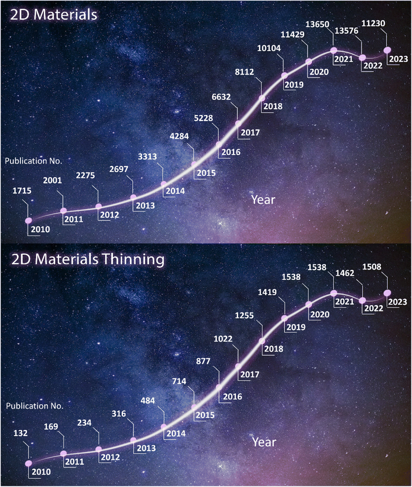 | ||
| Fig. 1 Annual publications on “2D Materials” and “2D Materials Thinning” (2010–2023). (Source: Web of Science). | ||
2. Atomical layer-by-layer thinning of 2D materials: advanced top–down strategies applicable to semiconducting devices
The band-gap values of 2D materials vary depending on the number of layers they have. For instance, while monolayer graphene lacks a band gap, the introduction of adlayers leads to a fascinating physical phenomenon called band gap via twisting50 and gate control.51 By these sophisticated strategies, the band gap could be precisely controllable. Simultaneously with the aforementioned strategies, layer-by-layer thinning of 2D multilayer materials through six strategies (see in Introduction section) is one of the best strategies for controlling the band gap following the number of layers. These thinning technologies offer several advantages: (i) they result in a cleaner surface by removing contaminants and residues, and (ii) they diminish the thickness of the 2D material film, potentially leading to alterations in the band gap with varying layer numbers. This is accompanied by modifications in the optical and electrical properties of 2D materials. Moreover, these advanced thinning strategies open up new possibilities for advanced electronic applications. There are a massive number of applications that ideally need defect-free single-layered 2D materials or defect-free multilayered 2D materials, and also, things that do not need the appearance of a bad-gap such as flexible displays, touch panels, solar cells, fuel cells, etc. Therefore, the latest thinning technologies currently being employed in 2D materials will be scrutinized (Fig. 2) in this section. Here, the operational mechanisms and assessments of the impacts of thinning techniques on the quality of the 2D material will be examined and clarified.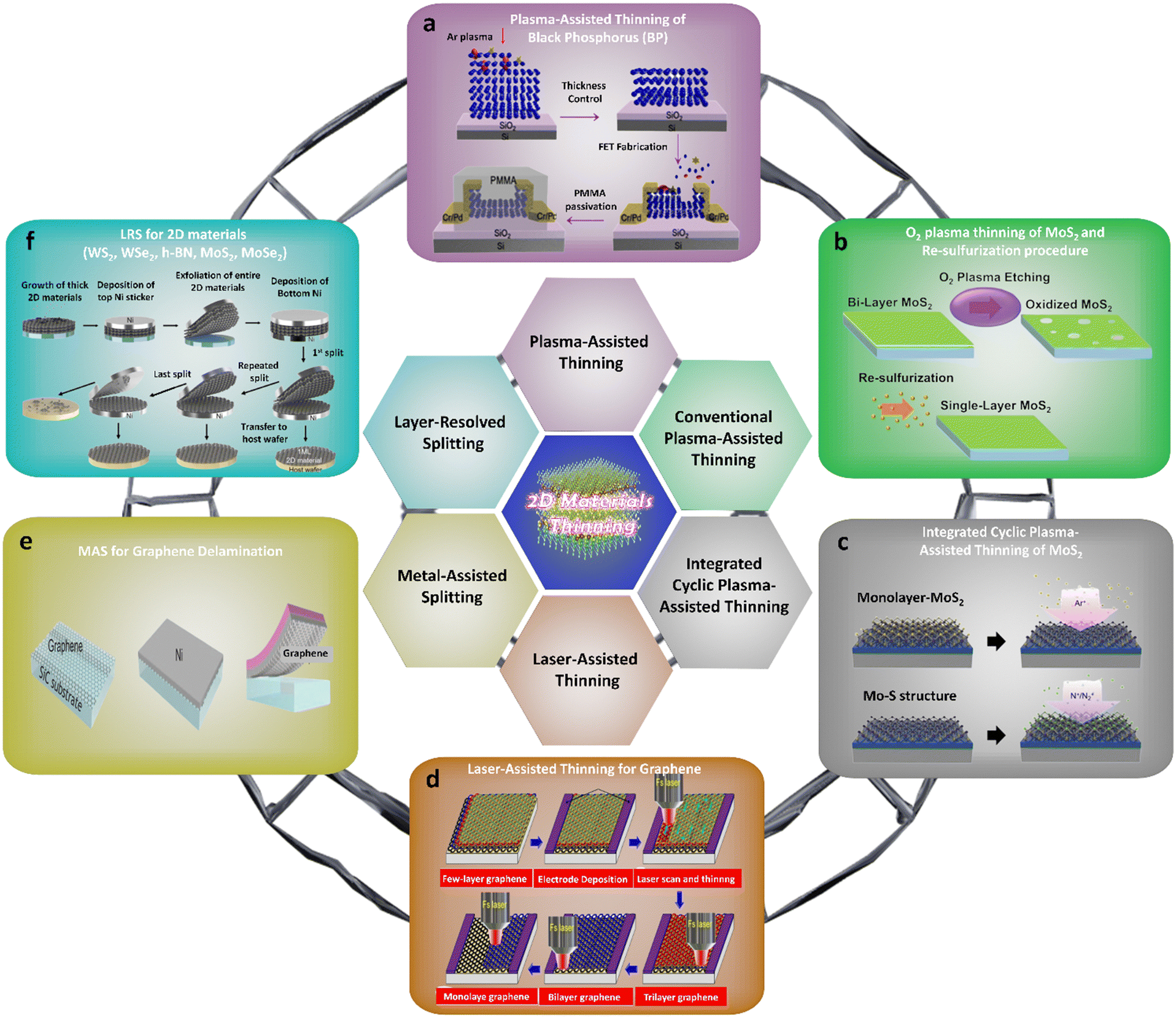 | ||
| Fig. 2 Atomical layer-by-layer thinning strategies of emerging intrinsic multilayer materials to date. The topmost representative top–down methods for intrinsic multilayer material thinning. (a) Schematic diagram of the plasma treatment of BP. Reproduced with permission from ref. 66. Copyright 2015 American Chemical Society. (b) The concept of oxygen (O2) conventional-assisted thinning for graphene. (c) Schematic of integrated cyclic plasma-assisted thinning for molybdenum disulfide (MoS2) thinning. Reproduced with permission from ref. 76. Copyright 2022 American Chemical Society. (d) Schematic of the femto second laser thinning method for graphene thinning. Reproduced with permission from ref. 83. Copyright 2013 Royal Society of Chemistry. (e) Schematic of metal-assisted splitting with an adhesive-strained layer of nickel (Ni) deposited on graphene. Reproduced with permission from ref. 88. Copyright 2013 AAAS. (f) Schematic illustration explaining the layer resolved splitting process for 2D material monolayer. Reproduced with permission from ref. 89. Copyright 2018 AAAS. | ||
2.1. Plasma technology-based thinning
Plasma can be produced by introducing energy into a gas using several techniques, including the application of electric fields, heating, or the exposure of the gas to extremely powerful electromagnetic radiation.52,53 Plasma has proven its potential to be applied in vast areas including chemistry, physics, engineering, microbiology, and medicine. Plasma-assisted thinning was introduced into integrated circuits manufactured in the 1960s and is widely applied even in the present day.54–57 In the field of materials thinning, in order to control the number of layers of materials, plasma will be combined with a CVD system to form a plasma enhanced CVD (PECVD). Here, PECVD utilizes electrical energy by radio frequency (RF) to create an electric field between the electrodes to generate a glow discharge (plasma) at low pressure (0.1–10 Pa). The sample is placed on a cathode electrode and then bombarded by ions which are accelerated by the self-bias.58,59 Thereby, Al-Mumen et al. have reported singular sheet thinning from bilayer graphene using O2 using the ground electrode plasma system regarding the various plasma thinning directions.60 However, this method introduced a few defects, due to the anisotropically vertical and horizontal thinning mode (Fig. 3a and b). Additionally, in this system, both the density of plasma (ions/area) and the kinetic energy of the ions are dependent on the power supplied to the lower electrode and cannot be changed independently.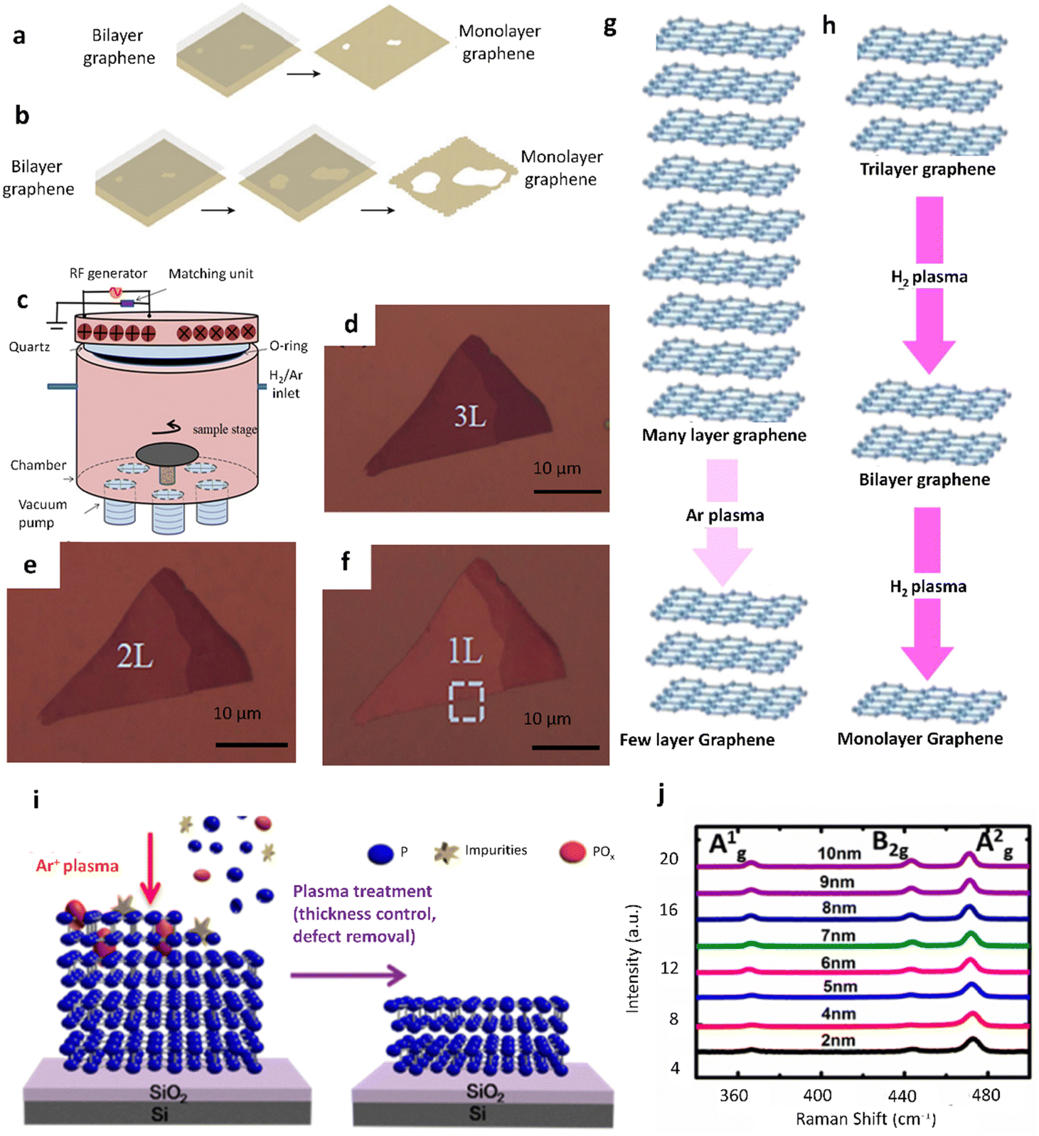 | ||
| Fig. 3 Plasma-assisted thinning of CVD multilayer graphene and black phosphorus (BP). Schematic of two possible graphene thinning mechanisms of ground electrode O2 plasma: (a) anisotropic vertical thinning and (b) anisotropic horizontal thinning. (a) and (b) Reproduced with permission from ref. 60. Copyright 2014 Springer. (c) The ICP system was illustrated with a vertically symmetrical design, featuring an annular gas inlet (H2, Ar inlet) at the top of the chamber and an annular gas outlet (connected to a vacuum pump) at the bottom of the chamber. (d) The graphene flake, consisting of 3 layers, was achieved after an additional 2 minutes of fine thinning. (e) The graphene flake with 2 layers, was obtained after another 1 minute of fine thinning. (f) The corresponding graphene flake with a monolayer after another 1 minute of fine thinning. (g) The schematic diagram illustrates the transition process from many layers of graphene to few-layer graphene using the fast-thinning mode, specifically Ar plasma. (h) The schematic diagram of the layer-by-layer thinning from trilayer to bilayer and finally to monolayer using a fine thinning mode, namely H2 plasma. (c)–(h) Reproduced with permission from ref. 65. Copyright 2018 Elsevier. (i) Schematic diagram of the effects of the plasma treatment of a BP flake: thickness control, and surface defect removal. (j) Raman spectra BP films with various thicknesses. (i) and (j) Reproduced with permission from ref. 66. Copyright 2015 American Chemical Society. | ||
A solution for this issue is inductively coupled plasma (ICP), where a separate coil is attached above the upper electrode and a separate RF power is applied to the coil. By first introducing the gas to the ICP coil and striking plasma there, the plasma density can be changed by adjusting the power provided to the ICP coil. Following the introduction of the ions into the chamber, they are propelled toward the lower electrode by using the biasing voltage created by powering the lower electrode, which also regulates the kinetic energy of the ions. These benefits and characteristics make ICP-plasma-assisted thinning become a potential system for achieving excellent anisotropy and high thinning rates.14,61–63 Recent studies by Pham et al. and Germain et al. have demonstrated graphene films, which can obtain less damage and are cleaned, by using chlorine (Cl) and nitrogen (N2) in the ICP system, respectively.15,16,20,64 In analogy to the report above, through the treatment of layer-by-layer thinning of graphene, Xiao et al. have succeeded in demonstrating a controllable number of layers of graphene. Here, graphene flakes were thinned using a planar low-frequency (0.5 M) ICP source (Fig. 3c) at room temperature. The plasma operated in the transition region between the capacitive discharge mode (E-mode) and the inductive discharge mode (H-mode) with medium input power (300–500 W). Hydrogen (H2) or argon (Ar) (at the flow rate of 10 sccm) gases were used as precursors at a flow rate of 10 sccm, and the working pressure was 3.4 Pa. Then, the defective samples were annealed in a tubular furnace under the protection of a N2-gas environment at high temperatures of 800–900 °C for 15 min followed by manual cooldown of the furnace to room temperature. The resultant trilayer, bilayer, and monolayer graphene formation was performed in three consecutive fine thinning steps of 2 min, 1 min, and 1 min, respectively, as clearly displayed in Fig. 3d–f. Consequently, a fast thinning mode is achieved under Ar plasma excitement in the transition region between the E-mode and H-mode. On the other hand, the fine thinning mode is considered to be suitable for layer-by-layer thinning of graphene, which is a characteristic of H2 plasma excited in the transition region between the E-mode and H-mode (Fig. 3g and h). The defects in graphene caused by direct ion bombardment can be nearly completely restored through subsequent annealing processes.65 Similarly, a few-layers of BP were also followed by Ar+ plasma treatment of various durations to achieve thickness-controlled BP films, as shown in Fig. 3i.66 The modification of BP was observed after the plasma treatments at 350 W, allowing for control of the BP thickness by adjusting the duration of plasma treatment without causing damage to the morphology and crystal structure of the developed films. The Raman spectra results shown in Fig. 3j depict the BP samples with thickness ranging from 2 to 10 nm. It exhibits vibrations of the crystalline lattice of BP and matches the Raman shift attributed to the A1g, B2g, and A2g phonons observed in bulk and exfoliated BP, which indicates that the BP films maintain their crystalline structures even after plasma treatment. Furthermore, the adjustment of the number of layers of 2D materials has been achieved via this method. Nonetheless, a significant limitation of this approach is the harsh environment at the surface–plasma interface, which can result in damage to the surface of the material's films. The continuous influx of plasma species leads to the accumulation of disorder and damage on the surface region.67 This is a major concern as not only more steps are required to form the thin 2D materials, but also a high precision thinning with minimal non-structural damage is needed. Any unwanted changes in the intrinsic multilayer material thinning process (layer numbers, profile) or excessive surface state density caused by plasma thin-induced damage would alter the behaviors and functions of semiconductor devices. Furthermore, parameters such as pressure, RF power, and selecting suitable plasma (O2, H2, Ar plasma) are also required and considered to avoid damage as well as defects throughout the thinning process.
O2, Ar and H2 plasma gas-assisted thinning. In a report, Chen et al. successfully achieved monolayered MoS2 from the sample originally with bilayer MoS2 through the ALT method.71 Here, after each 10 s of O2 plasma treatment, the uppermost layer of MoS2 only will detach from the sample (Fig. 4a). Due to the impact of the O2 plasma thinning process, the surface of the non-thinned layers in MoS2 may be influenced by O2 bombardment after the removal of the second layer of MoS2. This results in an uneven surface and numerous defects in the thinned MoS2. Nevertheless, as some positions in MoS2 now become oxidized MoS2, this can be rectified through an additional re-sulfurization procedure. Consequently, the remaining film, which initially contained partially oxidized MoS2 introduced during the layered thinning process, will be reverted to a complete MoS2 film through this re-sulfurization procedure. As shown in Fig. 4b, the influence of the O2 plasma treatment before and after the re-sulfurization procedure. An Mo6+ 3d3/2 peak located at ∼235.9 eV is observed, which indicates that a partial oxidation is introduced to the remaining MoS2 after the ALT procedure. After the re-sulfurization procedure, the Mo6+ 3d3/2 peak disappears, suggesting that the partially oxidized MoS2 film is converted back to a complete MoS2. With controlled time durations of O2 plasma treatment, it is possible to selectively thin off a single-layer MoS2 from the bilayer MoS2 sample. Furthermore, the authors have also constructed a heterostructure of WS2/MoS2 by using this method. The cross-sectional high-resolution transmission electron microscopy (HRTEM) of the un-thinned stripe and the thinned area away from the stripe edge are shown in Fig. 4c. The high-angle annular dark field (HAADF) mappings of the Mo and W elements are provided for both areas. The un-thinned stripe shows 7-layered 2D crystals, while the thinned area shows 3-layered 2D crystals. The difference in the number of layers corresponds to the thinning time using the 10 s O2 plasma treatment.
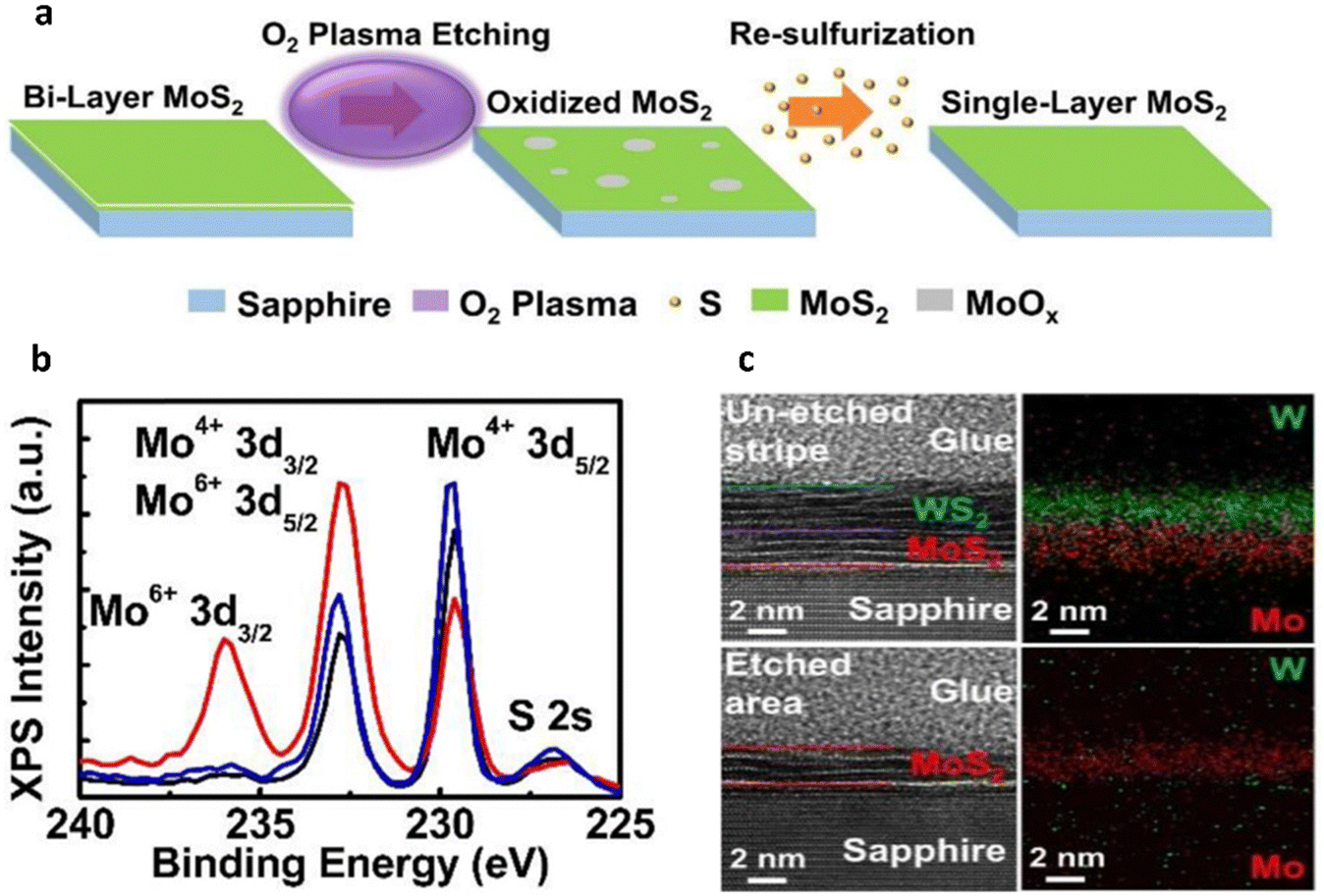 | ||
| Fig. 4 Conventional plasma-assisted thinning of CVD multilayer graphene and MoS2. (a) A diagram illustrating the step-by-step removal of MoS2 layers using O2 plasma treatment and the subsequent healing process through resulfurization. (b) The X-ray photoelectron spectroscopy (XPS) plots of the sample are presented in the figure, depicting three curves: the red line represents the sample treated with 10 s of O2 plasma before resulfurization, the blue line shows the sample after the resulfurization process, and the black line represents the as-grown sample. (c) The cross-section HRTEM images and their HAADF mapping of Mo and W elements of the samples; (a)–(c) reproduced with permission from ref. 71. Copyright 2017 IOP Publishing. | ||
MoF6 and H2O-assisted thinning. In an alternative approach, thermal ALT relies on self-limiting surface reactions and molecular modifications that create volatile byproducts for subsequent removal. This technique has demonstrated the ability to generate low surface defects and has found applications across various material systems. Similar to conventional ALT, the elementary steps in a thermal ALT process involve the physisorption and chemisorption of vapor-phase reactants onto the surface, followed by their chemical reaction and the desorption of by-products from the surface, providing sub-nanometer precision in the thinning process and earning recognition as an isotropic etching technology.72 An illustrative application of this method in thinning MoS2 was conducted by Soares et al.73 Here, molybdenum(VI) fluoride (MoF6) was introduced to the MoS2 sample in a controlled environment, serving as a fluorine source. The interaction of MoF6 with MoS2 led to the formation of volatile MoF6 and other reaction products. Concurrently, heat was applied to enhance the reactivity of MoF6 with MoS2, accelerating the chemical reactions and promoting the desorption of reaction by-products, including MoF6. Additionally, the presence of H2O can lead to reactions between MoS2, MoF6, and H2O, resulting in the generation of gaseous species containing all the elements (H2S, MoF2O2, HF, H2). This is synonymous with the fact that the layer-by-layer structure of MoS2 can be removed through these reactions (Fig. 5a). The controlled introduction of H2O further contributed to the precision of the thinning process. As a result, the authors successfully etched MoS2 films with a high degree of crystallinity and low defect density of the exfoliated flakes at 0.2 Å per cycle at 250 °C. Moreover, through AFM topography scans, the MoS2 samples were compared before and after exfoliation. Following etching at 200 °C, the author revealed localized topography changes and roughening along the edges of individual layers, resembling grain boundary decoration. Upon further examination of the MoS2 behavior on exfoliated MoS2 at an elevated temperature of 250 °C and the completion of an additional 90 MoS2 ALT cycles, a reduction in edge site roughness along the MoS2 layer perimeter was observed. Despite the initial loss of smaller crystalline domains, no significant topographic changes were identified on the flake (Fig. 5b–d). The absence of defects within the exfoliated flake could hinder available reactive sites for oxidation and subsequent etching, resulting in the observed lack of surface changes. This strategy shows promise for producing a high degree of crystallinity and low defect density in exfoliated flakes. It also proves to be a viable method for integrating 2D material thinning into high-volume manufacturing and is applicable to other layered 2D materials.
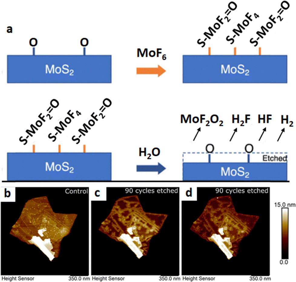 | ||
| Fig. 5 Thermal ALT of MoS2. (a) Schematic of MoS2 thinning using MoF6 and H2O. AFM images depicting the exfoliated flake of MoS2 without thinning (b), with an additional 90 cycles of thinning via ALT under 200 °C (c), and with an additional 90 cycles via ALT under 250 °C (d). Reproduced with permission from ref. 73. Copyright 2023 American Chemical Society. | ||
By incorporating these enhancements in adsorption and desorption processes, along with rapid gas-switching capabilities, notable improvements in cycle times can be achieved. However, some factors play a vital role in the ALT, such as ion energy, duration of thinning, and selecting the chemical adsorption and desorption. Using a very high ion energy leads to both the modified surface layer and the thinning of the underlying materials simultaneously, in contrast to using the very low ion energy, as the modified surface layer of materials is not possible to occur. Therefore, to attain the perfect thinning process, finding suitable conditions is one of the mandatory requirements.
Cyclic O2 radical adsorption and Ar desorption-assisted thinning. Kim et al. successfully generated a low energy O2-ion and a low energy Ar+-ion beam by floating the 1st grid of the ion beam source without applying any voltage, while the 2nd grid was grounded (Fig. 6a). The implementation of a two-step plasma thinning process in the ICP system, involving O2 radical chemical adsorption and desorption, along with Ar physical ion beam irradiation, significantly minimizes the damage on the graphene surface. The process was carried out with controlled-plasma energy reduced to 11.2 eV.74 As shown in Fig. 6b–f, a reduction in the thickness of the pristine bilayer graphene from approximately 1.45 to about 0.72 nm was observed after one cycle of thinning, as labeled by the yellow square. The roughness values before and after one cycle were around 0.41 nm and 0.43 nm respectively, whereas the average I2D/G was increased from ∼1.08 to ∼1.78, and the G and 2D peaks were red-shifted from 2679 to 2675 cm−1. These findings suggested that the removal of one layer of graphene is uniform across a large area without causing any noticeable damage to the surface of the graphene. In the same research direction, Lim et al. have elaborated that the modification of graphene thinning has been performed based on this strategy. During the process, 20 sccm of O2 is supplied from the ICP gun as an adsorbent in order to be reacted on the surface of the graphene, while applying 300 W of 13.56 MHz RF power. Then, 30 sccm of Ar was also supplied from an ICP gun using the same RF power for the desorption step (Fig. 6g).75 Consequently, the multilayered graphene was thinned with each monolayer of graphene. The optical transmittance results showed that the monolayer of graphene was completely removed, as evident in Fig. 6h, where both the G and 2D peaks disappeared, indicating the complete removal of bilayer graphene. Furthermore, after one cycle, the thinning process was observed in the graphene sheet composed of bilayer/monolayer graphene. In this case, only the unmasked bilayer graphene area changed to monolayer graphene, while the unmasked monolayer area transformed into zero-layer graphene, and the shape of bilayer graphene remained unchanged throughout the substrate (Fig. 6j). This proves that there was no undercutting of the graphene layer during the thinning process.
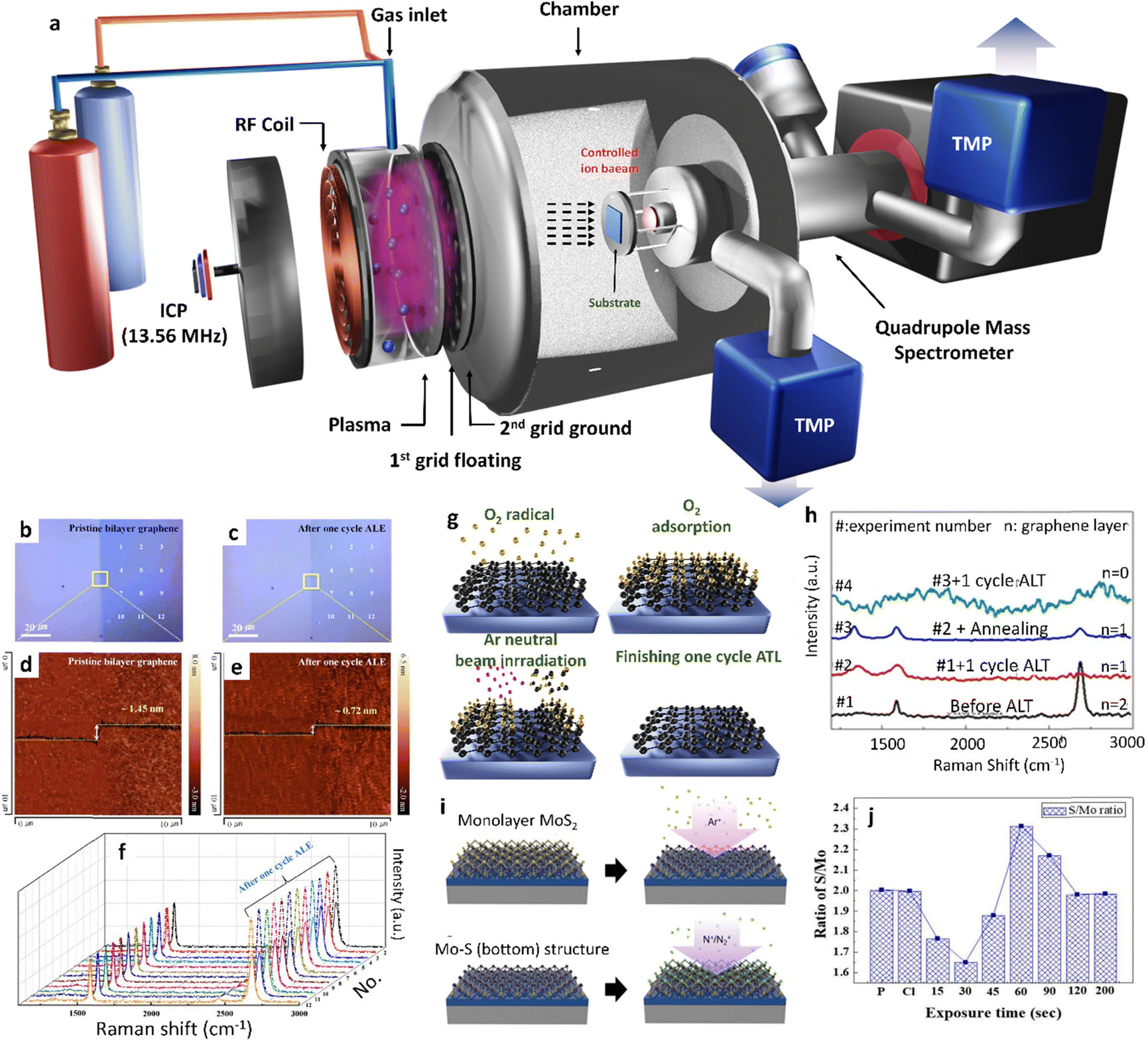 | ||
| Fig. 6 Integrated cyclic plasma-assisted thinning of multilayer graphene and MoS2. (a) The schematic illustrates a two-grid ICP beam system with an axial magnetic field, employed for graphene thinning, and a quadrupole mass spectrometer to measure ion energy and flux of the ion beam. (b) and (c) Optical image and (d) and (e) AFM images of the initial bilayer graphene, and after one cycle of thinning. (f) Raman data of the pristine bilayer graphene after one cycle for the corresponding white dots in (b) and (c). (b)–(f) Adopted with permission from ref. 74. Copyright 2017 Nature Publishing Group. (g) Three-atom-thick monolayer MoS2. (g) Schematic of thinning graphene by O2 radical absorption and desorption under Ar neutral beam irradiation. (h) Raman spectra of bilayer graphene measured after each cycle and after the annealing of the 1 cycle thinned graphene. (g) and (h) Adopted with permission from ref. 75. Copyright 2012 Elsevier. (i) Schematic of thinning MoS2, S top layer removal using a controlled Ar+ ion beam, and the Mo–S bottom structure after S top layer removal. Subsequently N2 chemical adsorption using a controlled N/N2+ ion beam on the Mo–S bottom structure. (i) Reproduced with permission from ref. 76. Copyright 2022 American Chemical Society. (j) Change of the S/Mo ratio on the MoS2 surface using X-ray photoelectron spectroscopy (XPS) during the thinning process. (j) Reproduced with permission from ref. 77. Copyright 2018 IOP Publishing. | ||
Cyclic Cl (or N2) radical adsorption and Ar desorption-assisted thinning. Likewise, the controlled method employs Cl− radical adsorption and Ar+ ion beam desorption per cycle for the layer-by-layer thinning of MoS2. This process effectively removes one monolayer of MoS2 uniformly without causing any damage or contamination.76 More specifically with the use of a controlled Ar+ ion beam coupled with a threshold ion energy of 25 eV, the top sulfur (S) layer alone was successfully removed from the monolayer MoS2 resulting in the formation of a new Mo–S structure and transits its phase from trigonal-prismatic 2H to metallic state (Fig. 6i). In addition, a p-type branch kind of expression was witnessed from the I–V studies of the semiconductor devices, if the removed S top layer is replaced by N atoms. Moreover, the estimation for the thinning time of each layer in MoS2 has also been presented in detail in reports by Kim et al. in 2018.77 The author provides a clear explanation that Cl atoms become trapped between S atoms and Mo atoms. Following Cl radical adsorption, the higher electronegativity of Cl in comparison to S leads to a significant decrease in the binding energy between the top layer of S atoms and the Mo layer. In Fig. 6j, during the Ar+ ion desorption, the layer containing S atoms is removed as S–Cl for the Ar+ ion desorption lasting for the duration ranging from 0 to 30 s. After the removal of the top layered S atoms, the trapped Cl ions form a bonding between Mo and Cl ions as Mn–Cl and Mo are removed, as Mo–Cl for the Ar+ ion desorption lasts for a duration of 30–60 s. Ultimately, the bottom S atoms bonded to the 2nd MoS2 layer through van der Waals force are left alone, and their binding energies are also reduced after the removal of Mo atoms. Consequently, the bottom S atoms are eventually removed during the Ar+ ion desorption with a duration of 60 to 120 seconds. This process could be continuously performed as a function of time for further thinning of MoS2.
Cyclic O2 radical adsorption and N2 desorption-assisted thinning. Besides, layer-by-layer of h-BN has been performed by Ma et al.78 The top layer of h-BN undergoes deformation due to the chemical bonding with O2 atoms. To rectify this, energetic N2 ions produced by a 100 W plasma are utilized for a 90 s duration to eliminate the deformed top layer of h-BN. (Fig. 7a–c). Fig. 7d displays atomic force microscopy (AFM) images of the h-BN flake subjected to single ALT processes. Both the as-transferred h-BN film and the film after a single cycle of ALT formed a smoother surface. The AFM height profile in Fig. 7e confirms that the h-BN film thickness remains unaffected after O2 processing, indicating that the applied O2 plasma does not thin the h-BN layer. On the other hand, the thickness of the h-BN film decreases by 3 Å following N2 plasma treatment, equivalent to the thickness of a single layer of h-BN. This suggests that the top layer of h-BN is removed after one cycle of the single ALT process. This study further investigated the impact of N2 plasma on another exfoliated h-BN flake to demonstrate that it does not physically thin pristine h-BN layers. These experimental results confirm that the role of O2 plasma treatment is to induce instability in the top h-BN layer, preparing it for the subsequent thinning process. Additionally, another mode of atomic layer thinning is also involved in a report by Kwon et al. through the use of ultraviolet (UV) light as an excited source for a photochemical reaction to form the oxide layer first and then using water to resolve phosphorus oxide.79
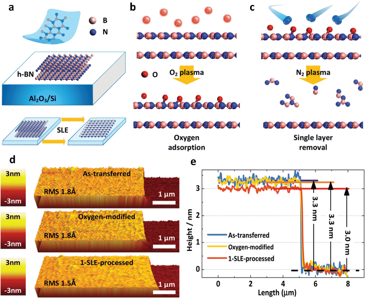 | ||
| Fig. 7 Integrated cyclic plasma-assisted thinning of multilayer h-BN. (a) The mechanical exfoliation method and the concept of single ALT are depicted in a visual representation. (b) The process of O2-adsorption, utilizing O2 plasma, is illustrated in a schematic. (c) A schematic showcasing the step of single layer removal, accomplished through N2 plasma. (d) AFM images of the h-BN are provided to demonstrate the single ALT process. (e) The thickness of the h-BN film is measured under three different conditions: as-transferred, O2-modified, and after undergoing one cycle of single atomic layer etching. (a)–(e) Reproduced with permission from ref. 79. Copyright 2019 Royal Society of Chemistry. | ||
Cyclic O2 adsorption and potassium hydroxide (KOH) desorption-assisted thinning. In an alternative approach, You et al. employed O2 and KOH as a wet method to thin WS2. The O2 plasma treatment, conducted for 30 s using a plasma cleaner in remote mode with a radio-frequency power of 50 W and a flow rate of 5 sccm, played a crucial role.80 Throughout the downstream plasma-based oxidation process, a protective WOx layer formed on the surface, acting as a passivation layer to impede further process.81 Following this, the WOx layer was selectively oxidized. Notably, WS2 oxidation proved to be a self-limiting elimination by reacting with a 1 M KOH solution for 60 s, revealing the underlying WS2. The self-limiting oxidation of WS2 occurred in either a single or bilayer, facilitating precise, atomical thin layer-by-layer removal. Consequently, the integration of remote O2 plasma treatment and the KOH wet-thinning process allowed for meticulous control of WS2 channel thickness in layer units by iteratively executing the recess cycle.
Integrating this technology could allow the construction of a unique structure in semiconductor devices, which leads to new breakthroughs in the electronic and optoelectronic devices fabricated by using 2D materials through atomic rearrangements, and it is possible to provide new advances for various applications through covalent bonding with rearranged functional groups within it.
2.2. Laser-assisted thinning
The laser-assisted thinning technique is a relatively new technique for modifying layers of 2D materials. Zhou et al. have successfully reported on thinning a multilayer graphene oxide (GO) film to a tri-layered film using laser-induced oxidative burning in an air environment. The laser thinning arose from the oxidative burning of the GO films in air.82 Here, the high-energy laser beam directly thinned down the functional graphene without using any lithography on it. This process consists of laser heat processing and cold processing. The working principle of laser heat processing technology is that the material is gradually melted and evaporated by local heating on the surface, while cold processing works by a photochemical reaction, which breaks the chemical bonds contained in the material when a high-energy laser radiates on the surface.Lu et al. have demonstrated a new approach for fabricating thinner graphene using this laser thinning technology, where graphene with a controlled number of layers was obtained through femtosecond (fs) laser thinning of few-layered graphene with single atomic layer precision,83 as shown in Fig. 8a. Here, the fs laser is employed and is integrated into a four-wave mixing (FWM) system, which allows for real-time monitoring of the laser thinning process using graphene's significant optical nonlinearity. By employing Raman spectroscopic mapping and characterization tools, differentiating monolayered graphene from bi-layered and multilayered graphene is very straightforward. However, distinguishing between multilayered graphene with various layer thicknesses is very challenging (Fig. 8b and c). Furthermore, the monolayered/bi-layered graphene is sensitive to the Raman I2D/IG ratio; in contrast, there is not much difference in the Raman I2D/IG ratio for few-layered or multi-layered graphene (Fig. 8d). In another innovation of Ermakov et al., the laser was used as an excited source to generate a heat sink on the surface of graphene for preventing the high-temperature region, which causes the burning and break down of C–C bonds, and leads to the reaction of carbon and O2 atoms in the surroundings, in order to become carbon monoxide (CO), carbon dioxide (CO2), and carbon trioxide (CO3) molecules (Fig. 8e and f).84 Thereby, the number of layers of graphene would be thinned from multi-layered graphene to single-layered graphene. The laser used in Raman spectroscopy can also be applied in thinning multilayered MoS2 to the monolayered one, which is similar to the thinning of graphene.85 Phosphorene oxides and suboxides with unique optical and fluorescence properties were produced on the top surface of laser-thinned BP in ambient environments.86 In this technique, the precision of laser heat processing is low, and this results in damage to the crystal, and the formation of rough and non-uniform surfaces and edges of the thinned materials. This is a quick thinning method with high precision; however, approximately 20% of the area of the graphene sheets from the first exfoliation exhibited a double-layered region (Fig. 9e–g). Thus, Au was utilized as a second adhesive-strain to selectively remove the double-layer region. As a result, the distribution of the 2D/G peak ratio revealed that 99% of the transferred graphene area, achieved through the two-step exfoliation process, consisted of a monolayered region (Fig. 9h–j). Inarguably, this method offers the advantage of being environmentally friendly, straightforward, and suitable for roll-to-roll processing, facilitating the transfer of large-area single-layered graphene onto flexible substrates. Nevertheless, there are still some limitations encountered using this technique, such as it depending on the thickness of the adhesive-strained layer. If the thickness of the metal tape is either too substantial or excessive, it can compromise the robustness required for the MAS process, resulting in an anisotropic cracking. Future developments based on this technique may promise to overcome as well as optimize the above issues, making it a simple yet highly effective technique for transferring graphene film at a low cost.
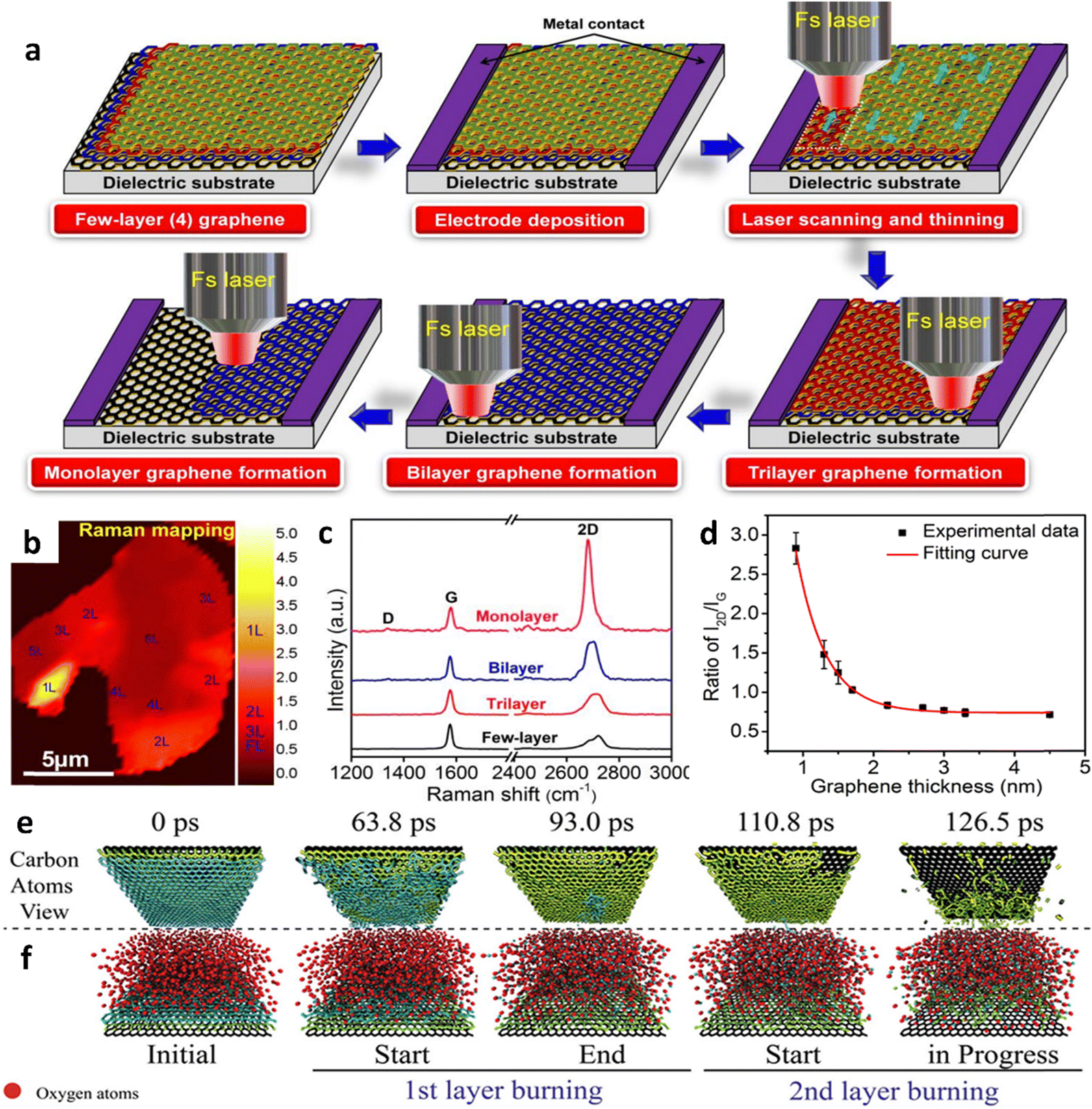 | ||
| Fig. 8 Laser-assisted thinning of CVD multilayer graphene. (a) The schematic illustrates the precise controlled thinning of few-layer graphene on a dielectric substrate using a fs laser, achieving single atomic layer precision. (b) Raman mapping of I2D/IG ratio was conducted on the selected region of graphene. (c) Raman spectra were obtained from single-layer, bilayer, trilayer, and few-layer graphene regions corresponding to the area in (b). (d) I2D/IG Raman peak ratio was analyzed as a function of graphene layer thickness. (a)–(d) Reproduced with permission from ref. 83. Copyright 2013 Royal Society of Chemistry. (e) Top and (f) side view of typical snapshots from atomistic simulations. In (e), O2 (red) atoms are excluded for clarity. These snapshots demonstrate that O2 initiates burning of the second layer only after the first one is almost entirely consumed. (e) and (f) Reproduced with permission from ref. 84. Copyright 2015 Nature Publishing Group. | ||
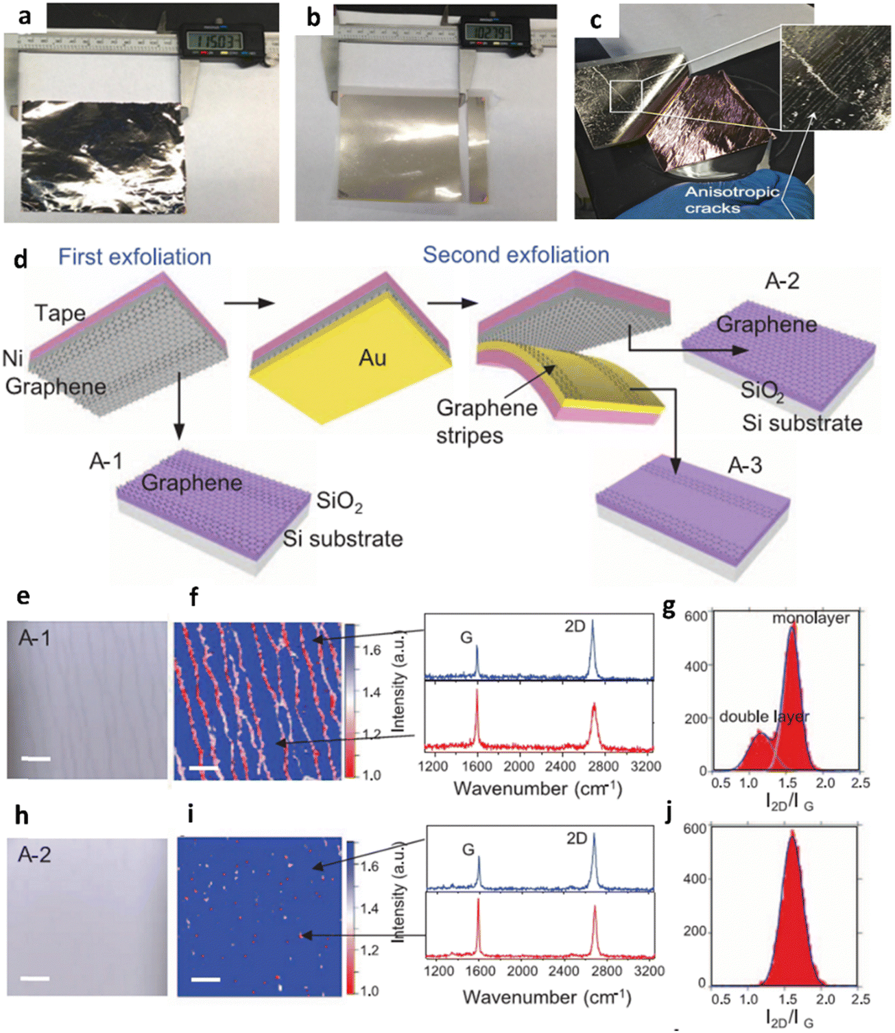 | ||
| Fig. 9 Metal-assisted splitting (MAS) of CVD multilayer graphene. Photographs depicting the consecutive steps of the MAS of graphene from (a)–(c). The process involves monolayer graphene on a Cu foil after: (a) metallization with Ni, (b) application of thermal release tape, and (c) peeling the metallized graphene off the Cu foil, revealing cracks shown in the insets. (a)–(c) Reproduced with permission from ref. 87. Copyright 2015 IOP Publishing. (d) A diagram illustrating a technique to eliminate double-layer stripes from graphene exfoliated from a SiC substrate. The process involves depositing a second adhesive-strained layer (Au) on the graphene/Ni/tape stack that was exfoliated from the SiC substrates. The Au layer selectively removes the graphene stripes forming double layers, resulting in a complete monolayer graphene sheet without the stripes. The monolayer graphene is subsequently transferred onto a SiO2/Si substrate (A-2). Moreover, the removed graphene stripes are transferred onto another substrate. Optical characterization was conducted on the graphene transferred after the first exfoliation (A-1), including an optical microscope image (e), a map of the 2D/G peak ratio from the Raman spectra (f), and a distribution plot of the 2D/G peak ratio (g). The results revealed that approximately 20% of the transferred graphene displayed a double-layer structure. Similarly, after the second exfoliation (A-2), optical analysis was performed, encompassing an optical image (h), a map of the 2D/G peak ratio from the Raman spectra (i), and a distribution of the 2D/G peak ratio (j). The findings indicated that the second exfoliation selectively removed the graphene stripes without causing any damage to the monolayer graphene. (d)–(j) Reproduced with permission from ref. 88. Copyright 2013 AAAS. | ||
2.3. Metal-assisted splitting (MAS)
Simpler techniques of producing thinner graphene are typically of interest, and one of the most promising ones is the MAS process, which produces a high-quality graphene film at a low cost and with ease through the controlled delamination of graphite layers. It entails weakening the van der Waals forces between graphene layers in order to enable their separation, which is accomplished by using a metal catalyst layer. Moreover, the selection of appropriate metals plays a crucial role, considering their interface binding energy with the graphene. Typically, metals such as Ni, cobalt (Co), and gold (Au) are commonly employed to cleave graphene due to their significant binding energies corresponding with that of the carbon in the MAS technique in the recent past as implemented by Zaretski et al. and Kim et al.87,88 A top-notch, smooth graphene film is produced through epitaxial growth using CVD on both metal foil and the silicon face of silicon carbide (SiC) wafers. A Ni film was carefully coated onto the graphene, followed by the application of thermal release tape. By gently lifting the thermal tape, the metal/graphene layers were effectively exfoliated from the underlying substrates, as illustrated in Fig. 9a–c. Thereby, Zaretski et al. have succeeded in splitting a single-layered graphene from Cu foil (Fig. 9d). Here, the Raman spectra studies have revealed that the 2D/G ratio of graphene is at 2700 cm−1 and 1580 cm−1, indicating the presence of monolayered graphene. Nevertheless, the rise in the D-peak intensity in the graphene transferred via the MAS process results from the mechanical harm caused during the metal-assisted exfoliation. This is not expected when the graphene film is not completely uniform. In another effort by Kim et al. to obtain high-quality monolayered graphene, Ni and Au adhesive-strained layers have been investigated to split graphene from the SiC substrate. Following the exfoliation of an epitaxial graphene layer from SiC using Ni as the initial adhesive-strained layer, a graphene film was obtained. However, the analysis of the 2D/G peak ratio distribution revealed that approximately 20% of the area of the graphene sheets from the first exfoliation exhibited a double-layered region (Fig. 9e–g). Thus, Au was utilized as a second adhesive-strain to selectively remove the double-layer region. As a result, the distribution of the 2D/G peak ratio revealed that 99% of the transferred graphene area, achieved through the two-step exfoliation process, consisted of a monolayered region (Fig. 9h–j).Inarguably, this method offers the advantage of being environmentally friendly, straightforward, and suitable for roll-to-roll processing, facilitating the transfer of large-area single-layered graphene onto flexible substrates. Nevertheless, there are still some limitations encountered using this technique, such as depending on the thickness of the adhesive-strained layer. If the thickness of the metal tape is either too substantial or excessive, it can compromise the robustness required for the MAS process, resulting in an anisotropic cracking. Furthermore, the damage of graphene could appear from mechanics during the metal-assisted exfoliation. This innovative technique may promise to overcome as well as optimize the above issues, making it a simple yet highly effective technique for transferring graphene film at a low cost.
2.4. Layer-resolved splitting
This method presents a universally applicable approach for thinning 2D materials on a wafer scale. The delamination process encompasses the initial growth of thick multilayer material on the wafer under relaxed growth conditions, succeeded by the extraction of multilayers into separate monolayers through a wafer-scale splitting process. In this method, 2D materials are initially grown on an arbitrary substrate using vapor phase epitaxy. Then, a thick metal film is deposited on the multilayer, and thermal release tape is applied on the metal as a handler. This process sets the stage for subsequent steps in the thinning procedure. By delaminating the tape-metal, the weakest layers of the 2D material-substrate interface are separated, resulting in the complete release of the entire 2D material film from the substrate. During the second stage, a metal layer is continuously added to the bottom of the 2D material film while preserving the top tape/metal/2D materials stack as exfoliated. Analogous to peeling the metal/2D materials stack off the substrate, a momentum is applied from the top metal to imitate spalling mode fracture, guiding the cracks downward. Due to the significantly higher interfacial toughness (Γ) between 2D materials and metals in comparison to that of the Γ2D–2D, cracks tend to propagate near the bottom metal, passing through the weaker 2D–2D material interface located directly above the bottom layers of the metal layer. As a result of the metal/2D materials stack separated during peeling, the bottom metal strongly adheres to the monolayer of 2D materials, leaving a monolayer of 2D materials on the bottom metal layer (Fig. 10a and b). Thereby, a report by Shim et al. has succeeded in the use of the LRS method to develop monolayered-tungsten disulfide (WS2) with the support of a 600 nm-thick Ni film.89 The iterative application of LRS resulted in the continuous production of a uniform monolayer WS2 film (Fig. 10c), evident from the spectra showing a rightward shift of the E12g peak compared to the initially exfoliated WS2 films (Fig. 10d) after three cycles. Following the third cycle, the remaining WS2 appeared as a non-continuous triangular domain on the Ni film, suggesting that the LRS process had reached the uppermost layer, where nucleated islands did not merge during growth.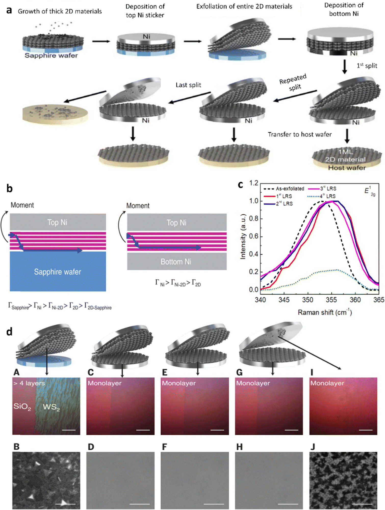 | ||
| Fig. 10 Layer-resolved splitting (LRS) of multilayer materials (WS2, h-BN, MoSe2, WSe2, and MoS2). (a) The LRS process for 2D materials is depicted in a schematic illustration. (b) The progression of cracks during LRS is presented in schematics for both the initial exfoliation of the entire 2D material from a sapphire wafer (left) and the exfoliation of the bottom monolayer 2D material (right). (c) Raman characteristics of WS2 films obtained through the LRS process. (d) Thinning of thick 2D materials into multiple monolayers through the LRS process and their subsequent characterization. The investigation includes optical micrographs (A, C, E, G, and I) and plan-view SEM images (B, D, F, and J) of the initially exfoliated thick WS2 [(A) and (B)], as well as monolayers of WS2 obtained after the first [(C) and (D)], second [(E) and (F)], third [(G) and (H)], and last [(I) and (J]) LRS processes, respectively. (a)–(d) Reproduced with permission from ref. 89. Copyright 2018. | ||
In analogy, the fabrication of a monolayer of hexagonal-boron nitride (h-BN), molybdenum diselenide (MoSe2), tungsten diselenide (WSe2), and MoS2 before and after the LRS process has also been presented and the results are shown in Fig. 11(a)–(h). Moreover, this method revealed the possible applications in the fabrication and investigation of materials into 2D heterostructure devices with quasi-dry stacking (Fig. 11i). Indeed, these heterostructure devices have demonstrated much consistent and uniform performance on the entire wafer. This high-throughput manufacturing of 2D heterostructures serves as a crucial stepping stone towards the commercialization of devices leveraging 2D materials
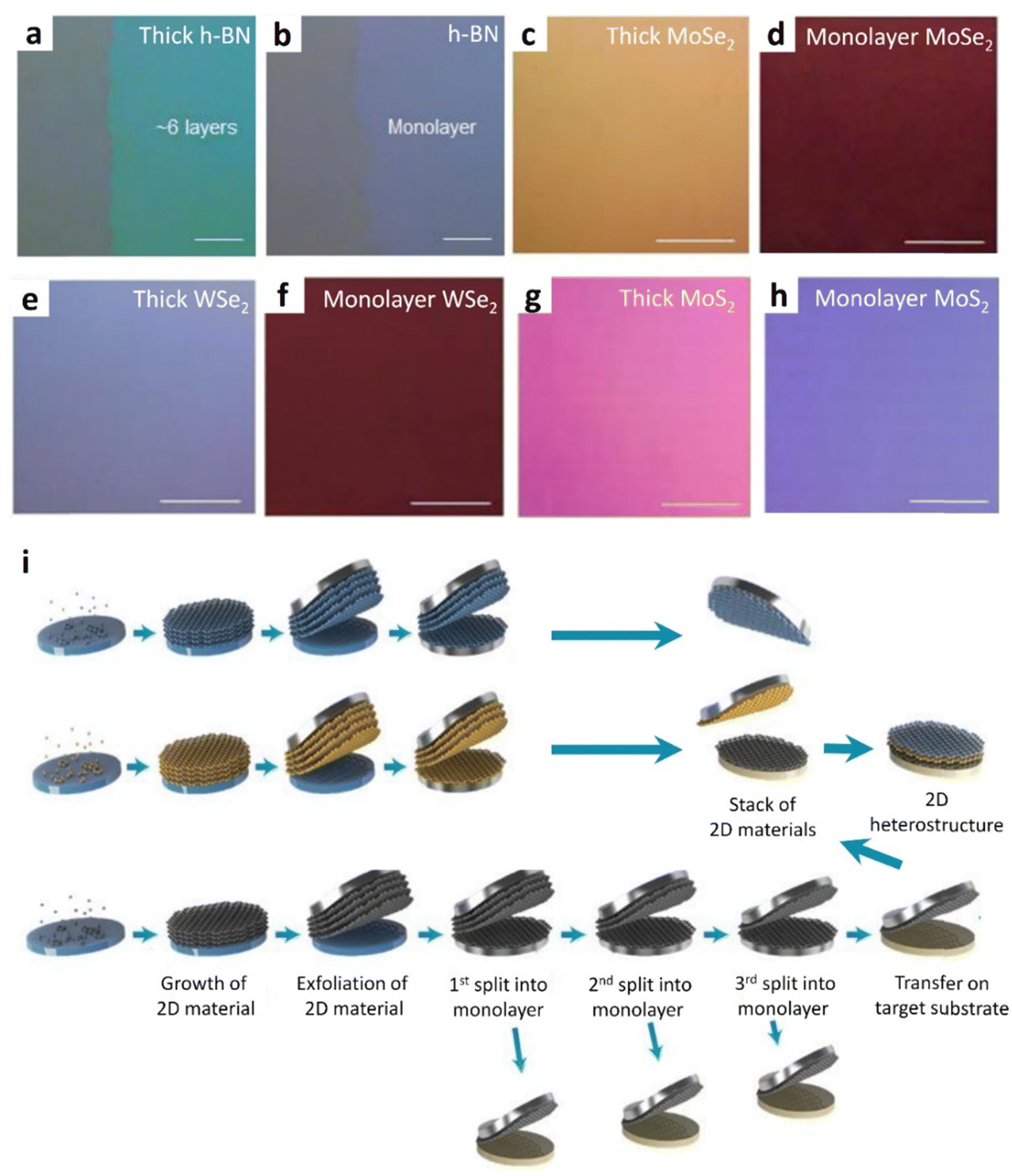 | ||
| Fig. 11 Layer-resolved splitting (LRS) of multilayer materials (h-BN, MoSe2, WSe2, and MoS2) and the relative 2D heterostructures. Splitting of 2D materials into a monolayer using the LRS technique. Optical microscopy images of thick h-BN (a), and monolayer h-BN (b); thick-MoSe2 (c), and monolayer MoSe2 (d); thick-WSe2 (e), and monolayer WSe2 (f); and thick-MoS2 (g), and monolayer MoS2. (i) Illustrations showcasing the creation of 2D heterostructures through the LRS process. A flow diagram demonstrates the step-by-step fabrication of the 2D heterostructure utilizing monolayer 2D materials obtained via the LRS process; (a)–(i) reproduced with permission from ref. 89. Copyright 2018 AAAS. | ||
3. Parameters that influence atomical layer-by-layer thinning of 2D materials
The thinning of 2D materials is a crucial process that significantly impacts their electronic, mechanical, and optical properties.90–93 One of the key parameters that influence the thinning process is the choice of the thinning processes, in which, the top–down thinning strategies have been presented in the above sections as the best solution, which can be employed to reduce the thickness of 2D materials. The selection of appropriate thinning methods depends on factors like material composition, desired thickness, and device applications. In addition, other parameters, such as the influence of technology, etchant type, and substrates also hold a vital role in determining the efficiency and controllability of thinning. Proper optimization of these parameters is essential for achieving high-quality, ultrathin 2D materials,94–98 enabling their integration into next-generation nanoelectronic and optoelectronic devices.99–1033.1. The influence of technologies
Thinning methods such as plasma-assisted thinning and ALT often use a plasma system for surface treatment. However, defects could be formed in the material, due to the etchant as it undergoes chemical reactions with the material's surface, leading to the removal of atoms or molecules from the top layers. The rate of these chemical reactions depends on the concentration of the reactive species, which is again directly influenced by the partial pressure of the etchant. For instance, in 2013, Geng et al. reported the formation of fractal and dendritic etched holes in a graphene film through the buffer gas of H2–Ar.104 Again, hexagonal etched holes were formed under high H2 partial pressure, whereas fractal etched holes with six branches were obtained while further decreasing the H2 partial pressure. This implies that in the process of layer-by-layer thinning of the material, the concentration or controlling ion beam is of paramount importance over the partial pressure of etchants for achieving precise control and ensuring high-quality thinning of 2D materials. This is also one of the reasons behind an integrated cyclic plasma-assisted thinning technique74,76,77,105–108 appearing and overcoming some limitations of plasma-assisted thinning and ALT methods in terms of the flux control. Here, a “double grid” setup refers to a specific configuration of electrodes used to control the ion density and distribution of the plasma.74,76,77,105–108 The double grid configuration is commonly employed to achieve better control over the ion flux and energy during the thinning processes, especially for delicate and precise thinning of 2D materials. As the reports mentioned above, the layer-by-layer thinning of 2D materials could be obtained using this method. However, the spacing between two grids and their configuration influences the electric field and ion trajectories within the plasma. Proper adjustment of the grid spacing and configuration is essential to achieve uniform ion density and energy distribution on the substrate surface. Additionally, all aforementioned four methods need to consider other parameters such as thinning time, temperature control, and post-thin treatments, which have impacted in achieving the high quality of the material.109,110 In contrast, the influencing parameters to obtain a high quality of 2D materials from MAS,87,88,111,112 and LRS89 methods mostly come from the metal catalyst choice. Because the metal catalyst interacts with the 2D materials at the interface during the delamination process, the nature of this interaction affects the adhesion between the catalyst and the material. A strong interaction enhances the efficiency of exfoliation, which leads to a higher success rate in obtaining the delamination of the layers. Additionally, the adhesion strength between the metal catalyst and the 2D material is also very vital. A metal catalyst with good adhesion promotes efficient and uniform delamination, resulting in high-quality, defect-free thinning. Moreover, the shear strength occurring at the interface of the catalyst and 2D materials further influences the ease of exfoliation. Cho et al. have reported comparative studies on the influence of selective metal catalysts on the exfoliated number of layers of WS2.113 In particular, through the exfoliation of Au and Ag layers, WS2 flakes with several layers have been obtained from bulk WS2. In this report, it has been clearly indicated that at the very same 10 layers of WS2, the adsorption of WS2/Au (∼0.93) is much higher than that of WS2/Ag (∼0.5), suggesting that the quality of the exfoliated WS2 from the Au layer is better. This result has demonstrated the importance of choosing a suitable metal catalyst for the removal of 2D materials with precise uniformity and purity in the LRS and MAS methods. To date, the integrated cyclic plasma thinning74,76,77,105–108 and LRS89 methods are considered as two of the best methods for fabricating 2D material thinning due to their advantages and unique capabilities in comparison to the other thinning methods such as plasma-assisted thinning, ALT, laser-assisted thinning, and MAS. Some of the parameters in these two methods can overcome the limitations that are involved in other methods. For example, in integrated cyclic plasma thinning methods, the double grid in ICP allows for precise control over the thinning process. The use of two grids, an extraction grid, and a bias grid, enables fine-tuning of the ion energy and ion density, leading to better control of the thinning rate and uniformity. The LRS method is able to control the formation layer-by-layer and is also considered as a non-invasive technique, as it does not require direct contact with the 2D material and thus, minimizes the potential damage to thinned materials. Plasma-assisted thinning and ALT methods make it very difficult to control the ion beam, which leads to damage on the surface of the material, while laser-assisted thinning is a non-contact and fast thinning process, but suffers from non-uniformity, localized thinning and metal-assisted thinning, which lead to the formation of cracks on the surface of the material. Therefore, considering the aspects of layer-by-layer thinning for 2D materials, integrated cyclic plasma thinning and LRS are the most preferable methods for integrating 2D material thinning due to their high controllability, scalability, and ability to achieve precise layer control. Nevertheless, the choice of the thinning methods depends on the specific 2D material, its properties, and the desired application. Each method has its unique advantages and may be more suitable for particular applications or material systems. Researchers often prefer to select the thinning method that best suits their requirements for achieving high-quality and tailored 2D materials.3.2. The influence of substrates
The substrate on which 2D materials are grown or transferred can have a significant influence on the thinning process. The choice of substrate and its properties can affect the overall quality, adhesion, and uniformity of the thinned 2D materials. In a comparison of using the different substrates for the thinning process of graphene, Yao et al. have demonstrated that under H2 plasma, uniform monolayer graphene was obtained on the Fe substrate after 10 minutes of thinning, while a shorter thinning time was observed on substrates of Ni, Co, and Cu with 5 minute, 5.5 minute, and 1.5 minute thinning, respectively. The findings suggest that H2 exposure plays a crucial role in reducing the carbon in metals and, effectively suppresses the precipitation process. This is particularly significant since the carbon solubility in metals follows the order: Fe (>25 at%) > Co (4.1 at%), Ni (2.7 at%) ≫ Cu (0.04%).114 In another report, the choice of substrates significantly influences the etching process of h-BN. For instance, Stehle's experiments demonstrated that the thinning of the bottom layer in h-BN, which directly contacts with the CuNi alloy substrate, occurs much faster in comparison to that of the upper layers.115 On the other hand, no thinning of multilayer hBN was observed while using a SiO2/Si substrate under the same experimental conditions. Currently, the exact mechanism by which the substrates affect h-BN thinning at the atomic level remains unclear, and further theoretical and experimental studies need to be explored for obtaining a controlled h-BN thinning.Overall, the choice and properties of the substrates have a significant influence on the thinning process for 2D materials. Adhesion, mechanical compatibility, chemical interactions, surface roughness, and thermal properties are some of the critical factors that are to be considered while selecting the substrate and designing the thinning process. Proper substrate preparation and control are essential for achieving high-quality, uniform, and defect-free thinned 2D materials that are suitable for various applications in nanoelectronics, photonics, and other fields.
3.3. The influence of etchants
An etchant is a chemical substance or solution used to selectively remove or dissolve material from the substrates. Etchants are commonly used in various industrial and research processes for material processing, surface preparation, and thinning of materials, including 2D materials. The choice of etchant depends on the material being processed and the specific goal of the process. In the context of thinning 2D materials, an etchant is used to selectively remove layers of the 2D material, reducing its thickness while preserving its properties. Different etchants are employed depending on the specific 2D material being thinned and the desired thinning technique. Felten et al. have reported using three types of gas precursors, namely: H2, O2, and carbon tetrafluoride (CF4), to obtain monolayered graphene via plasma treatment.116Here, the monolayered graphene appears to be less defective as revealed from Raman spectroscopic studies, whereas the CF4 plasma leads to functionalization without thinning and graphene becomes an insulator at saturation coverage. This occurs due to the absence of chemical thinning of carbon by F atoms and the presence of a large number of negative ions in CF4 plasma suggests that ion bombardment of the sample is not taking place, and CF4 plasma is an electronegative medium. In the case of H2 plasma, graphene is exposed to atomic H2 and other more energetic species such as H+ and H3+ ions. These positive ions can be accelerated towards the graphene and gain sufficient energy to surpass the hydrogenation barrier for both mono and bilayer graphene, resulting in a similar modification rate. Additionally, the reactivity of bilayer graphene was observed to be lower in O2 and CF4 plasma, whereas no such distinction is observed in the case of H2 plasma. However, in another report, Ghasemi et al. have mentioned not observing any changes in MoS2 flakes while using H2 plasma (H2 passivates sulfur vacancies), but a slow thinning rate is observed for O2 plasma (O2 physical thinness MoS2 through sulfur vacancies), and a high thinning rate (F free radicals react highly with MoS2 and thin it)117 is witnessed for sulfur hexafluoride (SF6) plasma.
Another significant influence may arise from the use of chemical etchants, particularly in the ALT technique. The careful selection of materials and an examination of their impact on the structure and bonding between them with the thinned 2D materials are crucial, as they can affect the material surface and properties of 2D materials. For instance, in obtaining monolayer graphene, a uniform monolayer C–O bonding must be formed on the high-oriented pyrolytic graphite (HOPG) surface. Kim et al.'s study demonstrated that increasing the exposure time to O2 radicals enhances the percentage of C–O bonding on the HOPG surface.118 Through Ar beam irradiation, the monolayer C–O bonding on the HOPG surface can be completely removed. After 1 minute of Ar beam irradiation, the carbon binding state of the HOPG surface transforms to 57 atoms % of sp2 C–C bonding and 43 atoms % of sp3 C–C, with no observable C–O bonding. However, the authors also observed that after one ALT cycle, the sp3 bonding formed after O2 radical adsorption was not fully recovered to sp2 C–C bonding. This is believed to be partially related to damage to the graphene substrate during O2 radical adsorption and Ar beam irradiation. The graphene surface can only be restored after annealing the etched graphene in an H2:He gas mixture. In another example of thinning MoS2 using the ALT method, Cl radicals are used and adsorbed on MoS2.119 As Cl is a better oxidizing agent than S, the adsorbed Cl weakens the covalent bonding between Mo and S. The Cl adsorption not only changes the Mo–S binding energy but also decreases the van der Waals force between the MoS2 layers. Ar+ ion bombardment during the desorption steps breaks the Mo–S binding and removes the broken MoS–Cl/S–Cl from the MoS2 surface. Raman spectra observations confirmed that after each ALT cycle, one monolayer of MoS2 can be completely removed without noticeably damaging the exposed MoS2.
Therefore, the choice of etchant is a vital aspect of the thinning process for 2D materials. Etchants affect the etching rate, selectivity of the enactment, surface morphology, and controllability of the thinning process. Proper selection and understanding of etchants are crucial for achieving high-quality, defect-free, and well-controlled thinning of 2D materials that are suitable for various technological applications.
4. Semiconducting devices associated with atomical layer-by-layer thinning of 2D materials
A plethora of 2D material-based electronic and optoelectronic devices with diverse functionalities, such as photodetectors, photodiodes, and field-effect transistors (FETs), have been developed. The integration of 2D material thinning into semiconductor devices has sparked tremendous interest from physicists/chemists/nanotechnologists, primarily owing to their ultrathin structure, robust light-matter interactions, and compatibility with existing Si photonic technology (Fig. 12 and Table 1).60,66,75,76,80,89,107,108,111,112,120–129 These 2D materials possess a wealth of electronic and optoelectronic properties, encompassing light emission, optical modulation, saturable adsorption, and electrically modulated field effect characteristics.130–138 Harnessing these unique properties, significant endeavors have been channeled towards the exploration of 2D materials-based on electronic and optoelectronic applications, capitalizing on the advantages that are offered by top–down thinning strategies. As the thickness of the material decreases to the atomic-length scale, vertical quantum confinement comes into play. This transformation from bulk to 2D planar introduces significant alterations in the material's electrical and optical properties, thereby enabling the realization of semiconductor devices that can be scaled down to ultrasmall sizes. For example, FETs and photodetectors utilizing various 2D materials have demonstrated significant potential for practical applications.139–148 Or even, using 2D materials with narrow bandgaps have been designed for infrared photonic devices, and exhibited impressive performance.149,150 In particular, 2D materials characterized by van der Waals-stacked heterojunctions and homojunctions exhibit compact dimensions, extremely thin profiles, straightforward fabrication, and unique physical phenomena, making them promising for utilization in electronic and optoelectronic applications.151–153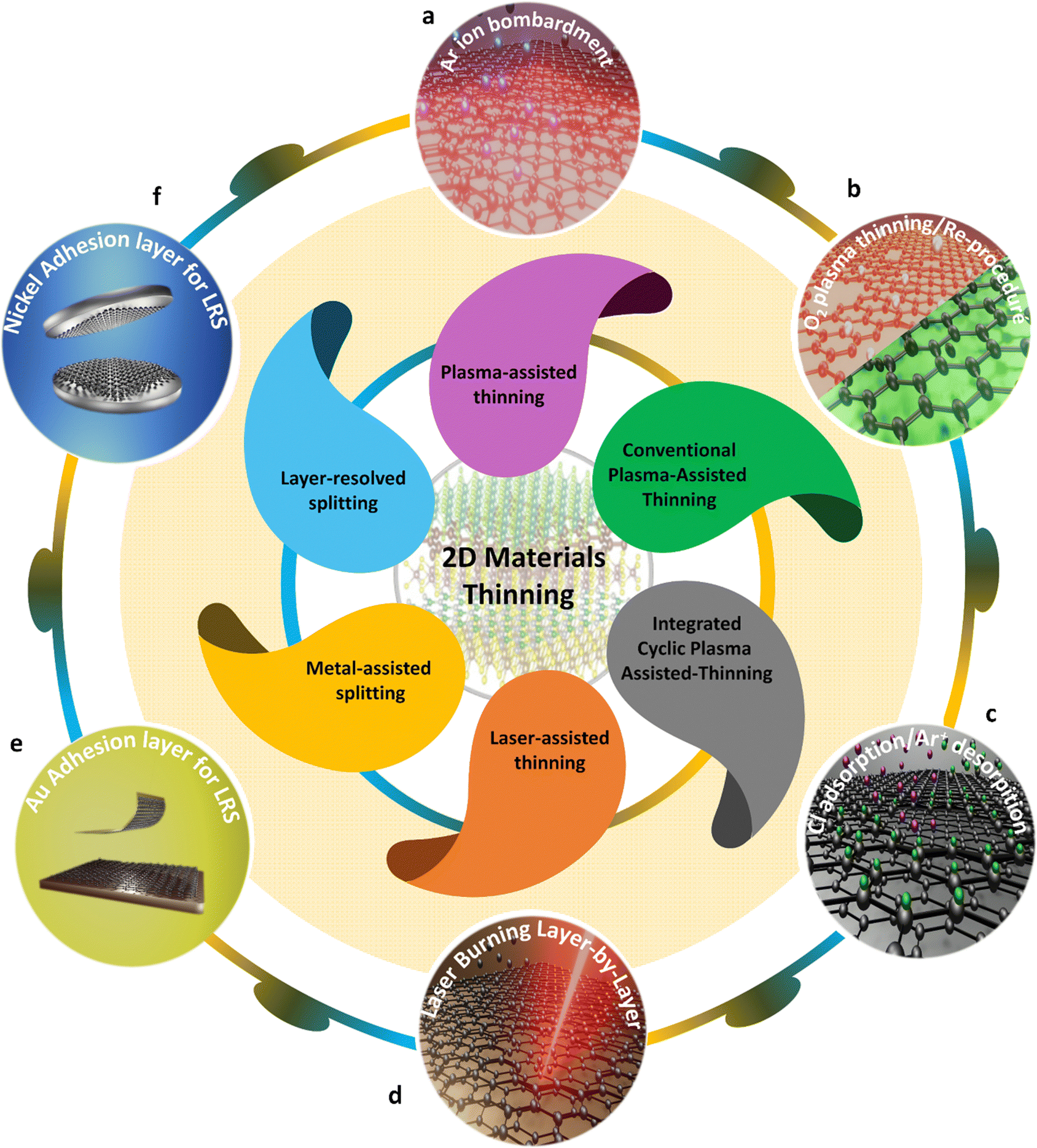 | ||
| Fig. 12 Modern layer-by-layer thinning technologies applicable to 2D materials utilizing: (a) plasma-assisted thinning, (b) conventional plasma-assisted thinning, (c) integrated cyclic plasma assisted-thinning, (d) laser-assisted thinning, (e) metal-assisted splitting, and (f) layer-resolved splitting. | ||
| 2D materials on substrates | Thinning strategy | Thinning parameters | Application of thinned 2D materials | Performance |
|---|---|---|---|---|
| Multi-layer graphene/SiO2 | Conventional plasma-assisted thinning + post annealing (Ar/O2) | 100 sccm N2 and 5 sccm Ar/O2 | Monolayer-deep pattern123 | Thinned graphene with good quality and few defects |
| Bi-layer graphene/SiO2 | Conventional plasma assisted thinning by ICP | 10 sccm O2, processing pressure of 313 mTorr to 326 mTorr | —60 | — |
| Multi-layer graphene/SiO2 | Conventional plasma-assisted thinning | 200 sccm Ar/H2, pressure 0.05 of mbar | —125 | — |
| Multilayer MoS2/sapphire and multilayer WS2/sapphire | Conventional plasma-assisted thinning | Pressure of 0.4 Torr with a 30 sccm O2 | A top-gate of WS2/MoS2 heterostructure transistor71 | High drain currents are observed for the device |
| Bulk BP/SiO2 | Conventional plasma-assisted thinning | Ar maintains the pressure at 30 mTorr | A few-layers of BP was used in FET66 | Achieved a high Ion/Ioff ratio of ∼105 at room temperature |
| Bi-layer MoS2/p-type Si | Integrated cyclic plasma-assisted thinning | 63 sccm Cl2, and 70 sccm Ar | Thinned monolayer MoS2 applied for FET107 | The field effect mobility was estimated to be 2.02 cm2 V−1 s−1 after one thinning cycle |
| Tri-layer graphene/SiO2 | Integrated cyclic plasma-assisted thinning | 20 sccm O2 and 30 sccm Ar | CMOS device75 | Poor electrical transport properties due to high energy damage |
| Multilayer WSe2/SiO2 | Integrated cyclic plasma-assisted thinning | O2 + Ar plasma | A lateral p–i–n homojunction based WSe2 diode127 | Open circuit voltage of 340 mW, a responsivity of 0.1 A W−1, and a specific detectivity of 2.2 × 10¹³ Jones |
| h-BN flakes/Al2O3/Si | Integrated cyclic plasma-assisted thinning | The gas flow is fixed at 400 sccm for both O2 and N2 | A gate dielectric based on a few layers of h-BN78 | The dielectric constant is about 3.5, which is similar to the earlier reports |
| Multi-layer WS2/SiO2 | Integrated cyclic plasma-assisted thinning | 5 sccm O2, 1 M KOH | FETs based thickness of WS280 | After eight recess cycles, the transfer characteristics exhibited as n-type behavior |
| Monolayer MoS2/p-type Si | Integrated cyclic plasma assisted-thinning of MoS2 | First grid 25 V, ion energy Ar of 25–28 eV | Removal of S top layer of monolayer MoS2 from the metal contact area of a Mo–S structure in FET device76 | The on/off ratio improved from 3.44 × 10⁵ to 2.24 × 10⁷ |
| Multi-layer MoS2/SiO2 | Integrated cyclic plasma-assisted thinning | Cl radical adsorption and Ar+ ion beam desorption per cycle | A mono/multi-layer nano-bridge multi-heterostructure through the selective layer control of multi-layer MoS2108 | A photodetector with ultrasensitive optoelectronic performances (photoresponsivity of 2.67 × 10⁶ at λ = 520 nm and 1.65 × 10⁶ A W−1 at λ = 1064 nm) |
| A few layers graphene/SiO2 | Laser-assisted thinning | Femtosecond laser excitation energy of 532 nm | —126 | The few layers of graphene obtained after transferring and micro ribbon of graphene formed from laser thinning without the formation of amorphous carbon. |
| Multilayer MoS2/SiO2 | Laser-assisted thinning | 532 nm of laser | Photodetector of MoS2 homojunction128 | At the maximum responsivity, the detection rate is 1.04 × 10⁹ Jones |
| Bulk MoS2/SiO2 | Metal-assisted splitting | — | Monolayer MoS2-based FETs111 | The high mobility (∼30 cm2 V−1 s−1) and large on–off ratio (∼107) |
| Bulk BP/SiO2 | Metal-assisted splitting | — | A few layers BP was used FET112 | The hole mobility of 68.6 cm2 V−1 s−1 and the current on/off ratio of 2 × 10⁵ |
| Bulk MoS2/Cu | Metal-assisted splitting | — | Multi-layer MoS2 was applied in solar cells129 | Reasonably good power-conversion efficiencies up to 2.8% under AM 1.5G illumination |
| Multi-layer MoS2/sapphire, multi-layer h-BN/sapphire, multi-layer WS2/sapphire, multi-layer WSe2/sapphire | Layer-resolved splitting of MoS2, h-BN, WS2, WSe2, MoSe2 | — | 2D heterostructure of monolayer MoS2/double layers h-BN based FETs89 | The FETs exhibited the field effect mobility from 6.3 cm2 V−1 s−1 to 12.8 cm2 V−1 s−1 |
However, contradictorily, the thickness during the fabrication of 2D material thinning is still very difficult to obtain cleanliness, less damage, and defects on the surface of the material, partly due to environmental influences and the synthesis process. Therefore, in this section, we summarize and discuss the developments of integrated 2D materials into semiconductor devices based on the thinning strategies for further clarification. In Fig. 12, the top–down thinning strategies could be applied for the fabrication of 2D materials integrated into electronics and optoelectronics applications with the desired properties in achieving specific targets.
4.1. Photodiodes and FETs using thinned graphene, black phosphorous (BP), and WS2 through conventional plasma-assisted thinning
Owing to its high carrier mobility, graphene is a novel form of electronic material, yet its zero bandgap and low absorption properties make it unsuitable for semiconductor technology.154–156 Extensive research efforts have been dedicated to both bridging and surpassing the graphene bandgap, resulting in remarkable advancements in this field. Extensive research has been conducted to tailor the graphene bandgap. For instance, Ohta et al. and Y. Han et al. have employed a dual-gate structure to control bilayers of graphene and introduced doping techniques for creating graphene nanostructures.157,158 Wang et al. have suggested a gas-phase chemical approach to reducing the thickness of graphene from its edges, thereby decreasing the material's surface area. They employed O2 plasma to oxidize graphene under high-temperature conditions in a reduced environment (H2, Ar, and NH3).159 In another application, BP films were fabricated with various thicknesses, which were obtained by applying Ar plasma treatment to it and integrated into FETs (Fig. 13a and Table 1).66 The characteristics of current–voltage indicated the p-type dominant behaviors. Besides, the decrease of layer number of BP enhanced the mobility of the device from 70 cm2 V−1 s−1 to 415 cm2 V−1 s−1, and the on–off ratio increased while decreasing the hysteresis (Fig. 13b). This enhancement can be ascribed to the synergistic effects of thickness reduction and the removal of defects through plasma treatment. For photodiode applications, achieving a high-performance diode relies on the presence of high-quality p–n junctions coupled with a low resistance. Using the 2D materials and integrating them into devices based on homogeneous p-type/intrinsic/n-type (p–i–n) is also interesting research. As an example, by utilizing O2 plasma treatment, the uppermost layers of WSe2 are oxidized, resulting in the formation of a substoichiometric tungsten oxide (WOx) layer, while the underlying WSe2 layers remain unaffected and unchanged.127 As a result of the oxygen-vacancy-induced abundant band gap state near the conduction band, oxygen-deficient WOx behaves as a highly conductive n-type semiconductor with a remarkably deep work function. Moreover, WOx exhibits a low-lying Fermi level, making it an efficient p-type dopant due to its strong electron-withdrawing ability. On the other hand, introducing n-type doping in WSe2 can also be accomplished.160 In addition, due to the Ar plasma thinning process, the bombardment of Ar+ ions leads to the formation of substoichiometric WSe2, namely WSe2−γ. Thus, the presence of huge vacancies of Se confers a substantial electron donor capacity to the interface of the WSe2−γ layers. Consequently, when a fully assembled p–i–n structure was implemented (Fig. 13c, d and Table 1),127 the resulting p–i–n diode exhibited exceptional photodetection capabilities. It showcased an impressive linear dynamic range of 48 dB, which is a remarkable responsivity of 0.1 A W−1, and an excellent specific detectivity of 2.2 × 10¹³ Jones when exposed to illumination. The limitation of plasma-assisted thinning, that is the damage to the surface of the 2D materials, could be overcome and replaced by studies associated with the formation of p–n, or p–i–n structures, which can be applied to electronics and optoelectronics (Fig. 12).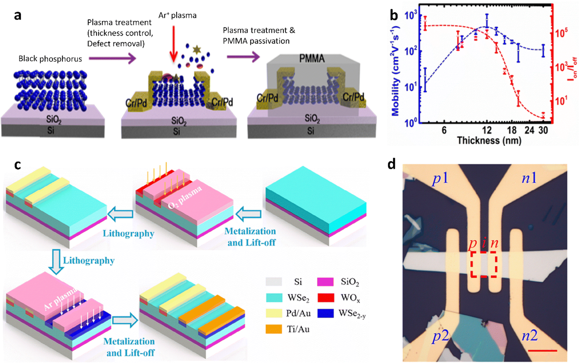 | ||
| Fig. 13 Plasma-assisted thinning for BP and WSe2 in FETs and photodiode devices. (a) Schematic diagram depicting the impacts of plasma treatment on BP flakes: device fabrication process. (b) The variation of current on/off ratio and field-effect mobility concerning the thickness of the BP film. (a) and (b) Reproduced with permission from ref. 66. Copyright 2015 American Chemical Society. (c) Three-dimensional schematic illustration of the process flow for the formation a p–i–n structure. (d) Optical image of the device. The scale bar represents 10 μm. (c) and (d) Reproduced with permission from ref. 127. Copyright 2021 American Chemical Society. | ||
4.2. FETs using thinned graphene, WS2, and h-BN through conventional plasma-assisted thinning
Lin et al. have made pioneering efforts on 2D material thinning into semiconductor devices via the ALT method. In this study, the ALT process was employed to fabricate CMOS devices with a graphene source, graphene drain, and graphene channel. To precisely control the number of graphene layers in the channel, a trilayer channel was selectively thinned through ALT, using an Au mask at the source/drain region (Fig. 14a and Table 1).75 The electrical characteristics revealed that reducing the number of graphene layers in the channel resulted in an increase in the channel resistance (Fig. 14b).161 In another report, the layer-by-layer thinning of WS2 is applied to CMOS devices, which is witnessed with very encouraging properties.80 The WS2 surface was treated by using remote O2 plasma, leading to the formation of WOx oxidation. Subsequently, a layer-by-layer removal of the target material is achieved through a selective reaction between the KOH solution and WOx. This selective reaction primarily targets the oxide layer, exposing the pristine WS2 surface (Fig. 14c and Table 1).80 Following ten recess cycles, the current–voltage output curves displayed characteristics of n-type behavior, with a noticeable increase in the number of electrons being induced into the channel as the gate bias was incremented in the positive direction (Fig. 14d). As efforts continue to enhance the gate dielectric in FET devices, h-BN has been emerging as a promising 2D dielectric material, offering the potential to fabricate high-performance devices. To achieve stronger gate control over the channel's potential, the thickness of h-BN plays a critical role, especially when it approaches just a few atomic layers. However, preserving the dielectric properties of the h-BN film presents a significant challenge. Nonetheless, Ma et al. managed to successfully obtain a monolayer of h-BN from an initial 8-layer h-BN flake using the ALT process.78 The capacitance of h-BN films exhibits an inverse relationship with their thickness. Other than the capacitance, another critical factors that influences the suitability of the film as a capacitive material is the leakage current flowing through the dielectric.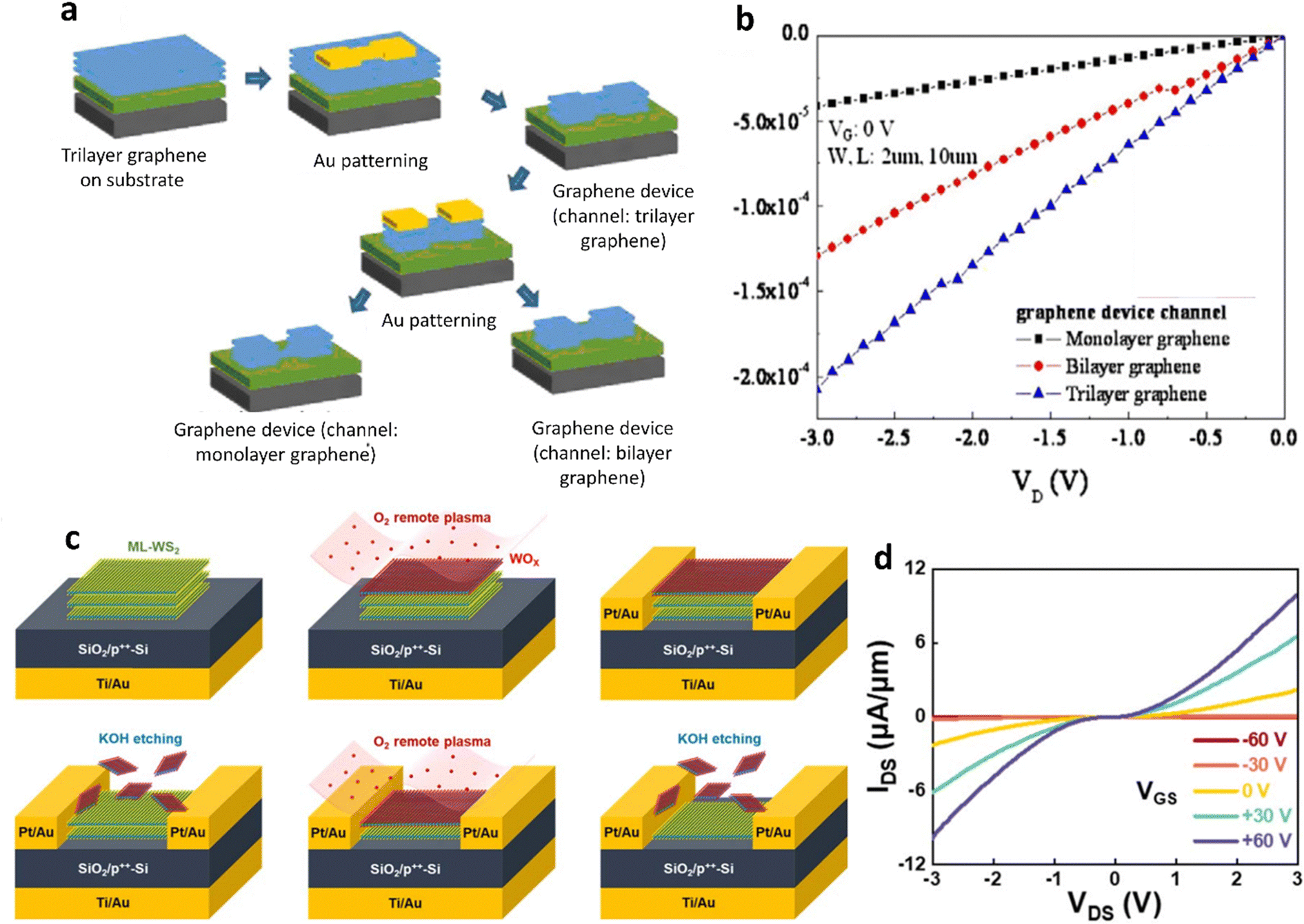 | ||
| Fig. 14 ALT for multilayer graphene and WS2 in FETs. (a) The process of creating a complete graphene device, consisting of a graphene source, graphene drain, and graphene channel, is described. (b) Drain current (ID)–source voltage (VD) measurements were conducted for various graphene device channel layers, with the device channel width set at 2 μm and length 10 μm. (a) and (b) Reproduced with permission from ref. 75. Copyright 2012 Elsevier. (c) Schematic illustrating the fabrication process employed to create the recessed-channel WS2 FET. Layer-by-layer thinning of the multilayer WS2 was accomplished using remote O2 plasma and a KOH solution. (d) Drain current (IDS)–drain-source voltage (VDS) output curves after 10 recess cycles. (c) and (d) Reproduced with permission from ref. 80. Copyright 2023 IOP Publishing. | ||
Although there have been some positive results, the investigated 2D material thinning into semiconductor devices via the ALT method is still difficult and challenging. In general, as the recess process is repeated a greater number of times to reduce the thickness of the 2D material channel, the on-current tends to decrease. Simultaneously, the width of the channel diminishes significantly with an increase in the number of recess cycles. Therefore, the optimal thinning process of ALT became very essential to produce 2D material thinning-based electronic and optoelectronic devices with high performance (Fig. 12).
4.3. Photodetectors and FETs using thinned MoS2 through integrated cyclic plasma-assisted thinning
The integrated 2D material into semiconductor devices based on the integrated cyclic plasma thinning method was introduced by Kim et al. in 2017.107 In order to assess the extent of damage to the monolayered MoS2 resulting from thinning the bilayer MoS2 using the one-cycle method, bottom-gate MoS2 FETs were constructed. The FETs were fabricated using exfoliated pristine bilayer MoS2, exfoliated intrinsic monolayered MoS2, and an exfoliated monolayered MoS2 obtained from one cycle of exfoliated bilayer MoS2. The MoS2 FETs showed drain currents versus gate voltages and estimated field effect mobilities for the exfoliated bilayer MoS2, exfoliated monolayer MoS2, and exfoliated bilayer MoS2 after one cycle: 5.78, 2.65, 2.03, and 2.02 cm2 V−1 s−1, respectively (Fig. 15a and Table 1).107 Notwithstanding, this method is also allowed to remove layer-by-layer MoS2, which means that S atoms of the top layer from the monolayer MoS2 could be completely removed to form a Mo–S bottom structure.76 Through the application of N+/N2+ ion exposure on the Mo–S bottom structure, a transformation to the p-type branch was achieved in the I–V curve, resulting in a field effect mobility of 40.3 cm2 V−1 s−1.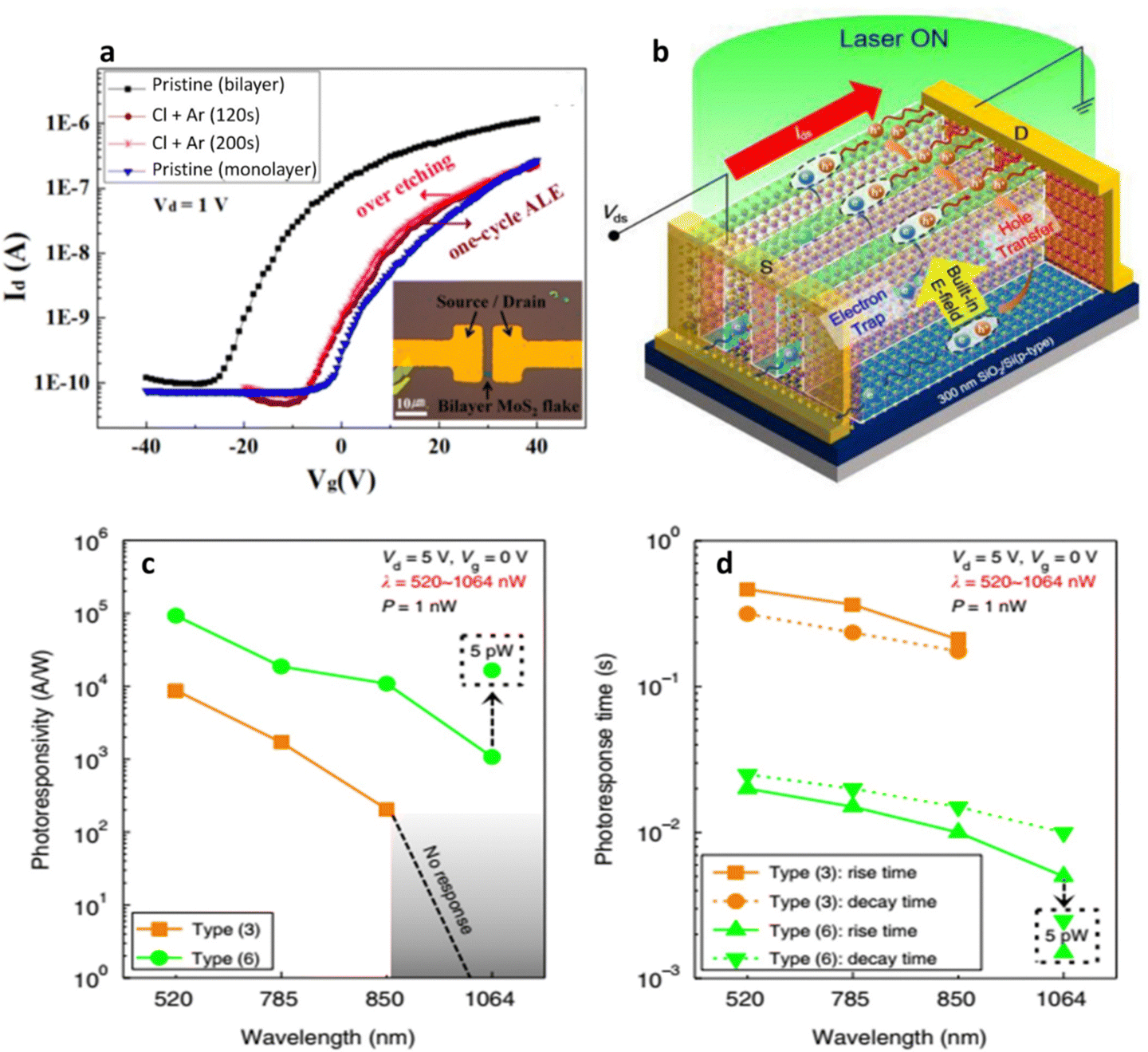 | ||
| Fig. 15 Integrated cyclic plasma-assisted thinning for multilayer MoS2 in FETs and photodetectors. (a) The drain current versus gate voltage characteristics of the bottom-gate MoS2 FETs were measured for different samples, including those fabricated with exfoliated bilayer MoS2, exfoliated monolayer MoS2, and exfoliated bilayer MoS2 after one cycle of MoS2 with 120 s (monolayer thinning conditions) and 200 s (over exposure Ar+-ion) of Ar+-ion exposure. (a) Reproduced with permission from ref. 107. Copyright 2017 American Chemical Society. (b) A schematic illustration depicting the carrier transport mechanism of the type (6) photodetector. (c) Comparison of the photoresponsivity and (d) photoresponse time for type (3) and (6) photodetectors across varying the laser wavelength, where type (3) represents the mono/multi-layer parallel heterojunction, while type (6) refers to a mono/multi-layer serial nano-bridge multi-heterojunction. (b)–(d) Reproduced with permission from ref. 108. Copyright 2019 Nature Publishing Group. | ||
In another application, an ultrasensitive photodetector of MoS2 has been reported with high performance.108 By employing a cyclic plasma thinning process, a series of nano-bridge multi-heterojunctions of MoS2, consisting of mono/multi-layers, were fabricated and utilized in the devices (Fig. 15b–d and Table 1).108 An ultra-sensitive photodetector exhibiting an excellent optoelectronic performance across a wide spectral range has been discovered in the recent past. It also witnesses a remarkable photoresponsivity of 2.67 × 10⁶ A W−1 at λ = 520 nm, and 1.65 × 10⁴ A W−1 at λ = 1064 nm. The nano-bridge multi-heterojunction, through a selective layer control process, has proven to be a crucial device technology with vast applications in broadband light sensing, highly sensitive fluorescence in broadband light sensing, highly sensitive fluorescence imaging, ultrasensitive biomedical diagnostics, and ultrafast optoelectronic integrated circuits.
Thorough and precise execution of the integrated cyclic plasma thinning process holds the potential to address the limitations of advanced 2D semiconductors in electronic and optoelectronic devices. This technique involves the replacement and rearrangement of atoms and the attached functional groups within the covalent bonding (Fig. 12).
4.4. Light-emitting diode (LED) and photodetectors using thinned WS2 and MoS2 through laser-assisted thinning
Laser-assisted thinning is known as an excellent method to thin down materials with high quality.162,163 Using confocal Raman spectroscopy as both the thinning laser source and the characterization tool allowed this method to become a simple, convenient, and rapidly obtained characterization technique of the same areas before and after thinning. In 2017, Bissett et al. reported that the photoluminescence (PL) yield of WS2 could be increased by up to 8-fold through a laser thinning procedure.164 Through controlling and repeating the thinning process, the increase of the PL spectra is shown as a function of layer number of WS2 (Fig. 16a, b and Table 1),164 which makes it suitable for use in LEDs. Furthermore, the laser thinning process not only removes the topmost layers of WS2, but also exposes the underlying layer, creating a highly reactive surface. This surface is rapidly passivated by atmospheric oxygen and water, resulting in dopants that increase the free carrier concentration of WS2. This, in turn, contributes to the enhancement of the PL intensity. The investigation between a few layers/multi-layers of MoS2via laser-assisted thinning to form a grating-like homojunction via selective laser thinning has also been performed in applications of photodetectors.128 Prior to the laser treatment, the output characteristic curve shows a slight nonlinear variation, mainly due to the presence of a weak Schottky barrier between the metal electrode and the multi-layer sample. However, after laser thinning, the devices exhibited characteristics resembling a p–n heterojunction, which is a significant application in the field of photoelectric detection (Fig. 16c, d, 12 and Table 1).128,165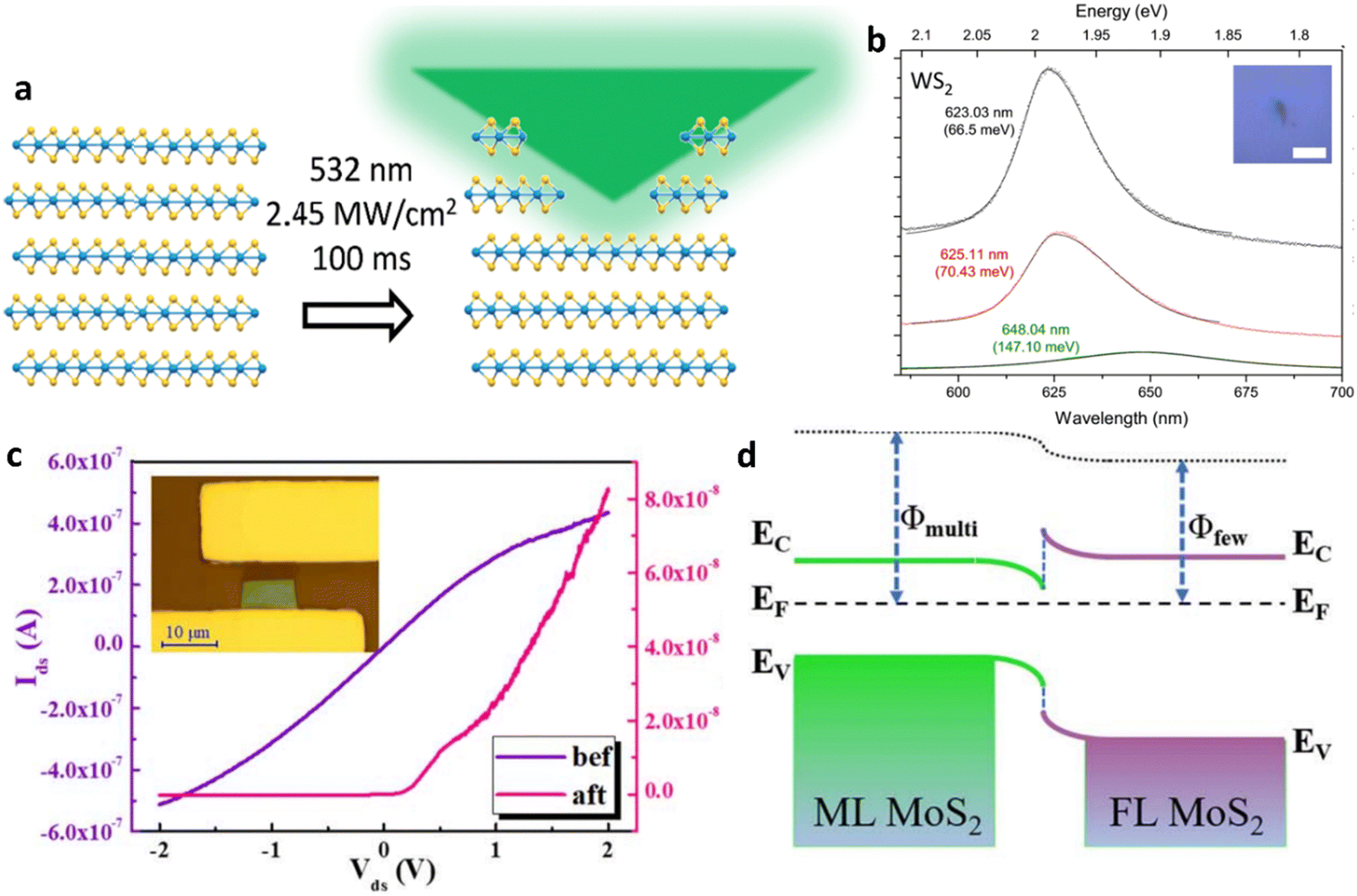 | ||
| Fig. 16 Laser-assisted thinning for multilayer WS2 and MoS2 in the enhancing of photoluminescence (PL) and photodetector devices. (a) Schematic showing the laser thinning of the WS2 layer. (b) PL spectra of the WS2 with repeated laser thinning. (a) and (b) Reproduced with permission from ref. 164. Copyright 2017 American Chemical Society. (c) Output characteristic curves before and after thinning. (d) Energy band diagram of a few layers/multi-layer homojunction of MoS2. (c) and (d) Reproduced with permission from ref. 128. Copyright 2023 IOP Publishing. | ||
4.5. Solar cells and FETs using thinned MoS2 and black phosphorous (BP) through MAS
Exfoliation using metal-assisted splitting has been on the market for a long time with the development of 2D materials. However, the reports mentioned are based on the applications of these methods that have been published and are not yet commensurate with the dramatic growth of 2D materials year by year. A recent invention demonstrated by Huang et al. was an Au/titanium (Ti) adhesion layer to control the number of layers of MoS2 in applications of FETs.111 Here, the authors demonstrated that the exfoliation method is not limited by the Au thickness and allows a large-area 2D crystal to be exfoliated using both conducting and non-conducting Au-coated substrates. Consequently, FETs can be directly constructed on as-exfoliated monolayer MoS2 channels. The FETs, regulated by an ionic-liquid top gate (Fig. 17a, b and Table 1),111 demonstrated excellent performance, with a high on–off current ratio (>106 at T = 220 K) and field-effect mobility ranging from 22.1 to 32.7 cm2 V−1 s−1. In addition, a superconducting transition was observed at 4.5 K, indicating the FET's promising performance. The device was directly fabricated on the ultrathin metal adhesion layer and also there is potential for further improvement (Fig. 17c). Monolayers or a few layers of BP were also exfoliated and integrated into FET devices using this method (Fig. 17d and Table 1).112 In contrast to the conventional scotch-tape method, the MAS method significantly enhances the yield of few-layer BP exfoliation by 100 times, yielding much larger BP areas. Moreover, the electrical properties of BP-FETs provide further evidence of the high quality of the few-layered BP, with a hole mobility of 68.6 cm2 V−1 s−1, and a current on/off ratio of 2 × 10⁵. Again, Wi et al. have successfully demonstrated multilayered MoS2 obtained from bulk MoS2 by applying the Cu adhesion layer to support the exfoliation process.129 By employing the plasma-assisted doping approach, the response of the solar cells was significantly enhanced. Furthermore, the research has demonstrated MoS2-based solar cells with remarkably high short-circuit photocurrent density values of up to 20 mA cm−2 and reasonably good power-conversion efficiencies of up to 2.8% under AM 1.5G illumination, as well as high external quantum efficiencies (Fig. 17e, f and Table 1).129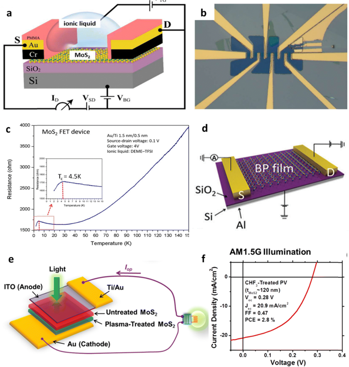 | ||
| Fig. 17 MAS for multilayer MoS2 and BP in FETs and solar cells. (a) The device structure of the MoS2 FET consists of a monolayer with an ionic liquid top gate. (b) An optical micrograph depicts the actual FET device with a monolayer MoS2 channel. (c) Temperature dependent I–V curve of a monolayer MoS2 device gated by ionic liquid at 4 V, the measurement temperature ranges from 2 K to 150 K. The inset is a zoomed-in I–V curve at temperatures from 2 to 15 K, from which a superconducting transition is indicated at Tc = 4.5 K. (a)–(c) Reproduced with permission from ref. 111. Copyright 2020 Nature Publishing Group. (d) Schematic of a BP FET device. S: source electrode; D: drain electrode. (d) Reproduced with permission from ref. 112. Copyright 2018 Royal Society of Chemistry. (e) Solar cell devices with MoS2 photoactive layers. (f) Current density–voltage characteristics, measured under the illumination of AM 1.5G simulated sunlight (power density, 100 mW cm−2). (e) and (f) Reproduced with permission from ref. 129. Copyright 2014 American Chemical. | ||
Even though it is a simple and economical method, the exfoliation using the MAS from bulk crystals has not been deemed technologically scalable so far (Fig. 12). However, as this technology becomes increasingly consistent, producing 2D layers solely determined by the source of the crystal's dimensions and crystallinity, materials research may shift its focus towards optimizing high-quality layered bulk crystal growth. Ironically, the fabrication of 2D materials for applications has been a long agenda followed by other thinning strategies, notably successful in Si technology, where the extraction of wafers from large, high-quality single crystals has been demonstrated for industrial applications.
4.6. FETs using thinned MoS2/hBN and graphene/WSe2 heterostructures through LRS
LRS is a technique involving the deposition of metal thin films onto the surface of a bulk crystal, enabling the formation of a robust and uniform bond between the metal and the surface layer of the crystals. Metals such as Au or Ni are commonly evaporated to exfoliate various monolayers, and this method facilitates the easy transfer of the exfoliated monolayer onto a different substrate. LRS holds potential applications in the fabrication of semiconductor devices and research exploring the intrinsic properties of 2D materials (Fig. 12). This strategy was developed as a layer-resolved technique to separate stacks of few-layered thick 2D materials grown on a Si wafer. The 2D material-based FETs using the LRS techniques were also introduced by Shim et al.89 FETs were formed by quasi-dry stacking a heterostructure of MoS2 and h-BN multilayers on a SiO2/Si wafer (Fig. 18a and Table 1).89 Besides, the comparison between FETs with and without containing the h-BN has also been evaluated. Despite having a high on–off ratio (>107), the FETs without h-BN suffered from significant hysteresis in their drain current-gate voltage sweep, hence negatively affecting the performance of their transistor operation. However, FETs with h-BN demonstrated considerable suppression of hysteresis (Fig. 18b). Furthermore, the FET arrays with h-BN exhibited a remarkable reduction in hysteresis during a gate voltage sweep applied uniformly across the wafer (Fig. 18c and d). Likewise, the advantage of the quasi-dry stacking process was also emphasized by the fabrication of array WSe2/graphene FETs, which exhibited a high on/off current ratio (Fig. 18e and f).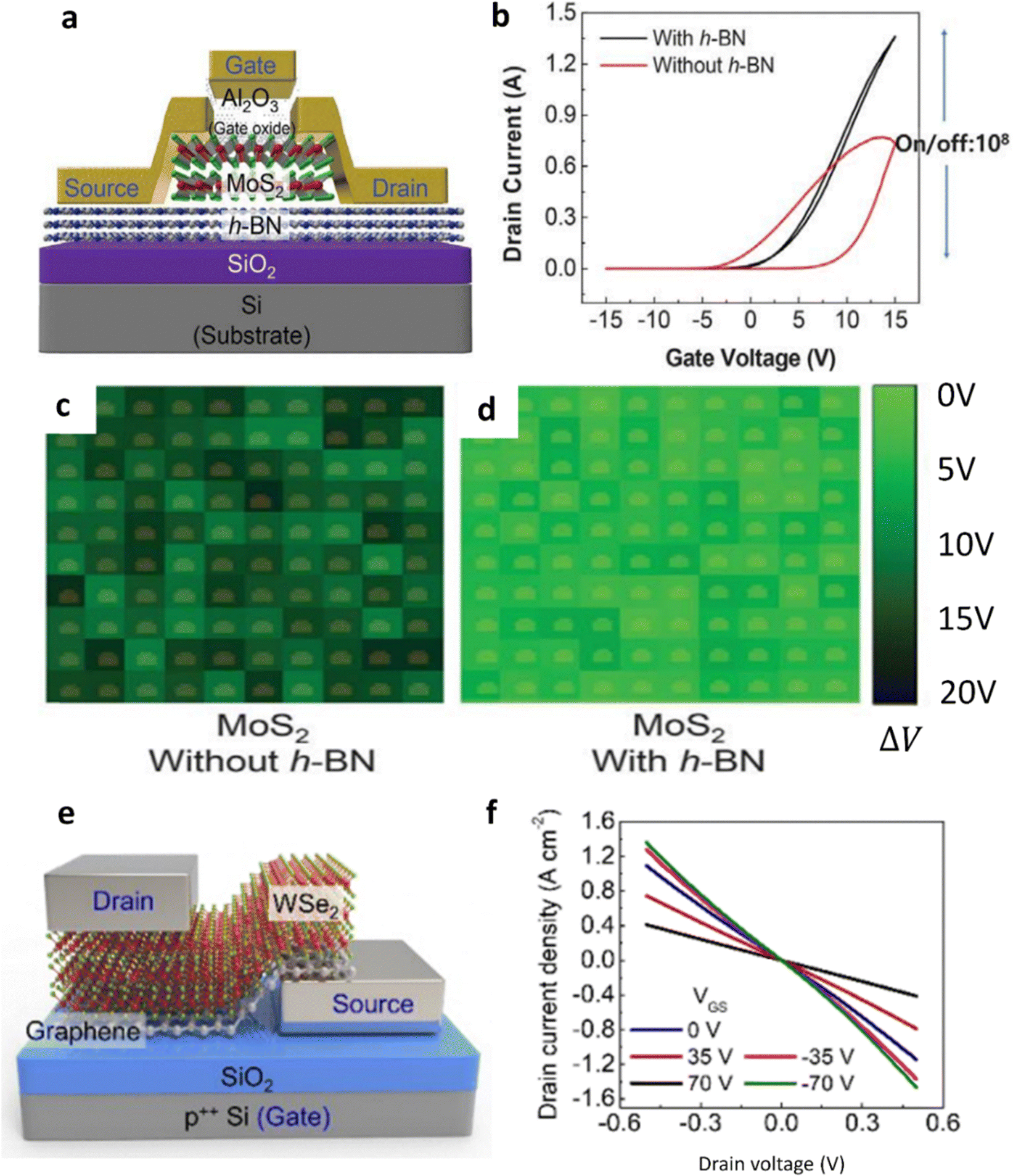 | ||
| Fig. 18 Layer-resolved splitting for multilayer MoS2/h-BN and WSe2/graphene heterostructures in FETs. (a) Schematic of MoS2/h-BN-based field effect transistor. (b) Exemplary drain current–gate voltage (ID–VG) characteristics of the MoS2/h-BN-based FET at VDS = 1 V. (c) and (d) 2D color maps illustrating the hysteresis voltage extracted from ID–VG curves at VDS = 1 V in transistor arrays fabricated without h-BN (left) (c) and with h-BN (right) (d), respectively. (e) Schematic of the graphene/WSe2 vertical transistor. (f) ID–VD characteristics measured as VGS from −70 V to 70 V with a 35 V step. (a)–(f) Reproduced with permission from ref. 89. Copyright 2018 AAAS. | ||
In general, all aforementioned thinning strategies make it possible to obtain 2D materials thinning and integrate them into semiconductor devices. The approach to the limitation of 2D materials could generally appear and bring breakthroughs in the application of electronics and optoelectronics. As a result, the thinning strategies are a suitable solution to obtaining high quality 2D materials.81,166–174 In particular, the integrated cyclic plasma thinning demonstrated by Kim et al. was supposed to be the most viable method to attain layer-by-layer 2D materials as well as less damage and defects on the surface material. Nevertheless, the integrated 2D material thinning using the top–down strategies still encounters some problems, which need to be addressed in the coming days. For instance, the LRS and MAS are typically not scalable for large-scale production. Furthermore, it is also challenging to achieve uniform thickness and quality across a large area, leading to device-to-device variations. Other factors such as surface, and edge roughness are also very important and can have high sensitivity to defects and chemical functionalization. Top–down approaches often result in irregular and rough edges, which can decrease the performance of the devices and can introduce scattering sites for charge carriers. Moreover, the top–down processes for thinning 2D materials can result in significant loss of the material and low yields for device fabrication, making it less economical- for large-scale production. Moreover, these processes are enabled for controlled and tailored thinning of 2D materials to achieve desired properties for specific applications. In addition, the consideration and selection of the thinning method in the fabricated semiconductor devices must be matched and consist of those created through bottom–up growth techniques, which can offer higher material quality and uniformity. Despite these limitations, the top–down thinning strategies remain crucial for research, prototyping, and generating a proof-of-concept for making semiconductor devices using 2D material thinning. As the field of 2D materials synthesis and processing evolves, efforts are being made to address these limitations and improve the overpack quality and scalability of thinning strategies for 2D materials in semiconductor devices applications.
5. Conclusion and outlooks
2D material thinning is a viable building component for usage in semiconductor devices due to its superior physical and chemical properties brought forth by its distinctive structure.25,29,175–177 The manufacture of 2D material thinning with the specified layered numbers and regulating structure is necessary to realize their practical uses.178 In fact, thinning technologies have been demonstrated to obtain 2D material thinning, including a few layers, bi-layer, or even monolayer. There are transfer methods that are currently available that do not involve thinning, making it feasible to move 2D materials from the growth substrate to a Si substrate. This integration of 2D materials with Si microelectronics presents a promising technological avenue for creating efficient and cost-effective systems. Such advancements could play a pivotal role in next-generation electronics and optoelectronics.179–181 Moreover, thinning has been demonstrated to have various applications, such as understanding the growth mechanism, identifying defective sites in 2D materials, enhancing material quality through thinning-regrowth approaches, increasing grain size via controllable nucleation density, and promoting heterojunction growth. Consequently, gaining profound insights into the thinning of 2D materials holds significant importance in advancing our understanding of the fundamental mechanisms behind graphene growth and enabling controlled processes for thinning 2D materials.Recently, substantial advancements have also been made in comprehending the thinning process of 2D materials.182–186 A general model of 2D material thinning has been established on the atomic scale through plasma-assisted thinning, ALT, and integrated cyclic plasma thinning, which have been successfully applied to get 2D material thinning. Using these methods leads to a reduction in the number of layers due to the bombardment of ions such as H2 and Ar with low energy or adsorption and deposition of the reaction gas injected onto the material surface, which reacted with as well as destroyed chemical bonds on the surface of the 2D materials. Contrastingly, laser-assisted thinning is a non-contact and non-chemical process, which uses the energy of a laser as an excitation source for the burning of 2D material layers. For applications to transfer and exfoliate 2D materials to arbitrary substrates, MAS and LRS are two of the most popular methods. Here, due to the support of a metal film, such as Au or Ni deposited on the 2D materials, the monolayer could be obtained via the peeling of the metal film supported by a thermal tape layer. In fact, each thinning technique revealed its own merits and demerits that they encountered throughout the fabrication process of 2D material thinning, as shown in Fig. 19. Thus, depending on the purpose and use of the 2D materials, selecting, and using a suitable method for applications to achieve high efficiency and optimization is necessary.
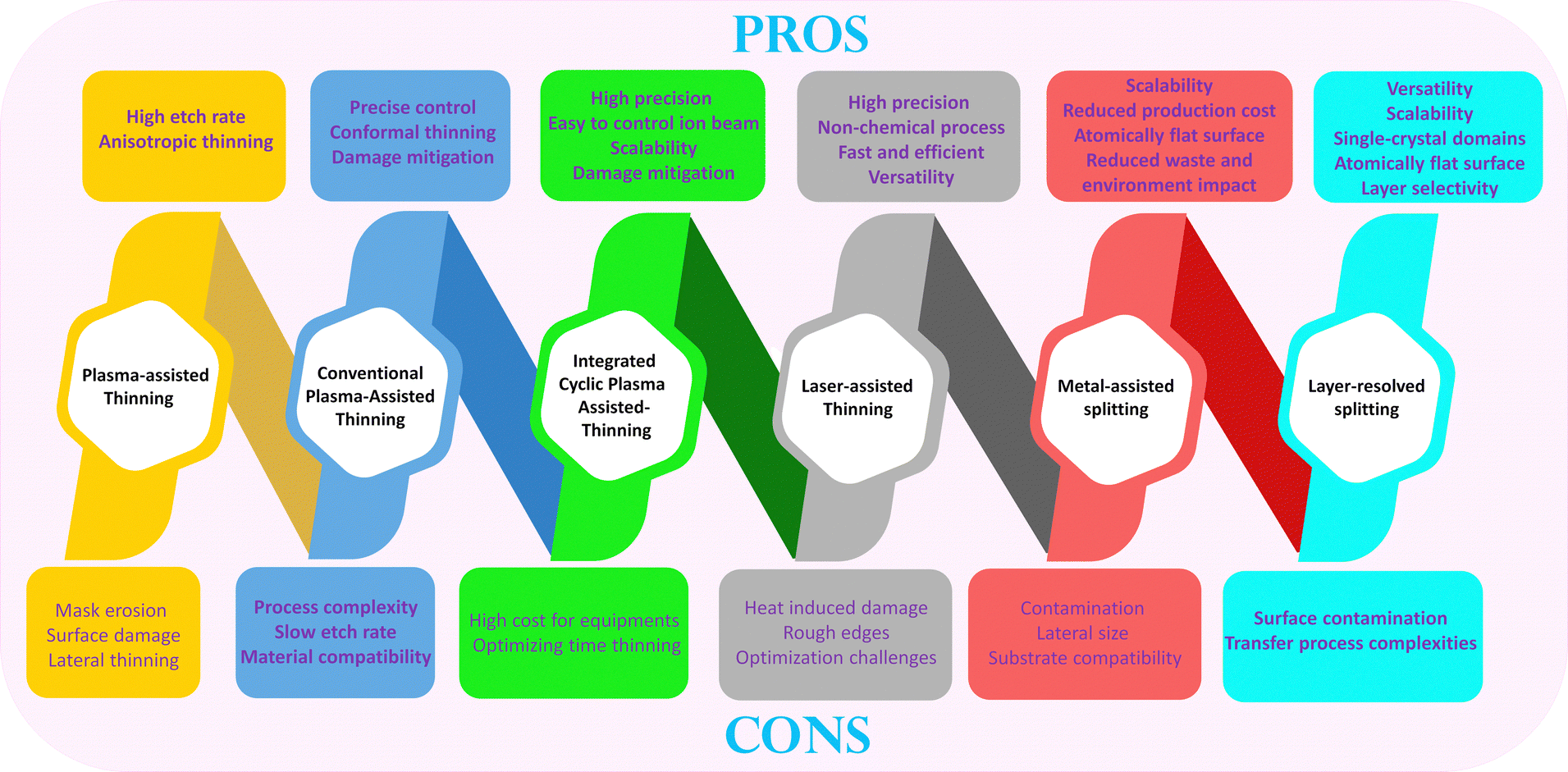 | ||
| Fig. 19 Pros and cons of thinning/splitting strategies of 2D materials. | ||
In addition, various experimental factors such as H2, Ar, or O2 partial pressure, etchant species, substrate, and buffer gas have also been observed to significantly influence the thinning behavior of 2D materials. Extensive theories have been explored and the mechanisms underlying the effects of parameters on 2D material thinning have been shown, but similar studies in another material thinning are still rare if these thinning methodologies are not only applied to 2D materials, but also applied to other materials and investigated for semiconductor devices such as polymer materials,187–193 transition metal carbides, nitrides, carbonitrides (MXenes),194–199 perovskite,200–204 or thinning metal-based nanowire, nanotube, and nanorod structures.205–207
The thinning advances in processing materials have the potential to open up new opportunities for the development of high-quality 2D materials that are needed for electronics and optoelectronics for suitable applications. The controlled band gap of 2D materials can lead to significant improvements in the current on–off ratio, PL, and other unexplored exotic properties. The layer-by-layer thinning of 2D materials by integrated cyclic plasma thinning technology is regarded as the most promising method due to its minimal physical and chemical damage. Research in this direction will be of great importance. Moreover, new thinning techniques such as crystallographic thinning,208–211 or metal-assisted chemical thinning,212–215 are also well worth waiting for in the fabrication of thinned materials. However, for the applications of 2D material thinning, they need more time to demonstrate the exactness, and stability in the future and if successful, it could open routines for new thinning strategies with low cost and high quality. In the context of future technological advancements, the potential application of thinning top–down strategies holds significant promise. This approach involves streamlining and optimizing complex systems, processes, or devices by strategically removing unnecessary components, layers, or functionalities. By identifying non-essential features, redundant components, and excessive layers of materials, the top–down thinning strategies can easily design devices that offer the same functionality but with a smaller environmental footprint and enhanced user experience. This might involve leveraging artificial intelligence and machine learning algorithms to dynamically adjust device settings based on individual usage patterns, thus conserving power and optimizing performance. The thinning top–down strategies could also be beneficial in sectors like transportation. With the development of self-driving cars, the integration of numerous sensors, processors, and communication systems can lead to a highly complex and potentially unwieldy vehicle architecture. Apply thinning strategies could help prioritize critical safety components while minimizing the layer number of materials, leading to more reliable and efficient autonomous vehicles. Energy storage is another area where 2D materials hold promise.216–222 Thinning strategies could be utilized to optimize the thickness and structural uniformity of 2D material-based electrodes in batteries and supercapacitors. This could improve energy storage capacity and cycling stability, addressing challenges related to volume expansion and contraction during charge–discharge cycles. In optoelectronics, 2D materials exhibit remarkable light-matter interactions that could lead to highly efficient photodetectors, solar cells, and light-emitting devices.223–229 By using thinning top–down approaches, it may be possible to fabricate ultra-thin, flexible, and transparent devices that efficiently harness and manipulate light at the nanoscale. This could open up new avenues for applications in wearable technology, displays, and advanced imaging systems. As illustrated in Fig. 20, various electronic and optoelectronic systems that could use graphene or other material thinning in contemporary devices are highlighted and projected future trends till 2030 such as power-gate transistors, quantum computing, or ferroelectric memory. These thinned 2D material-based devices could potentially be given the topmost attention in the coming time from the research community.230–237
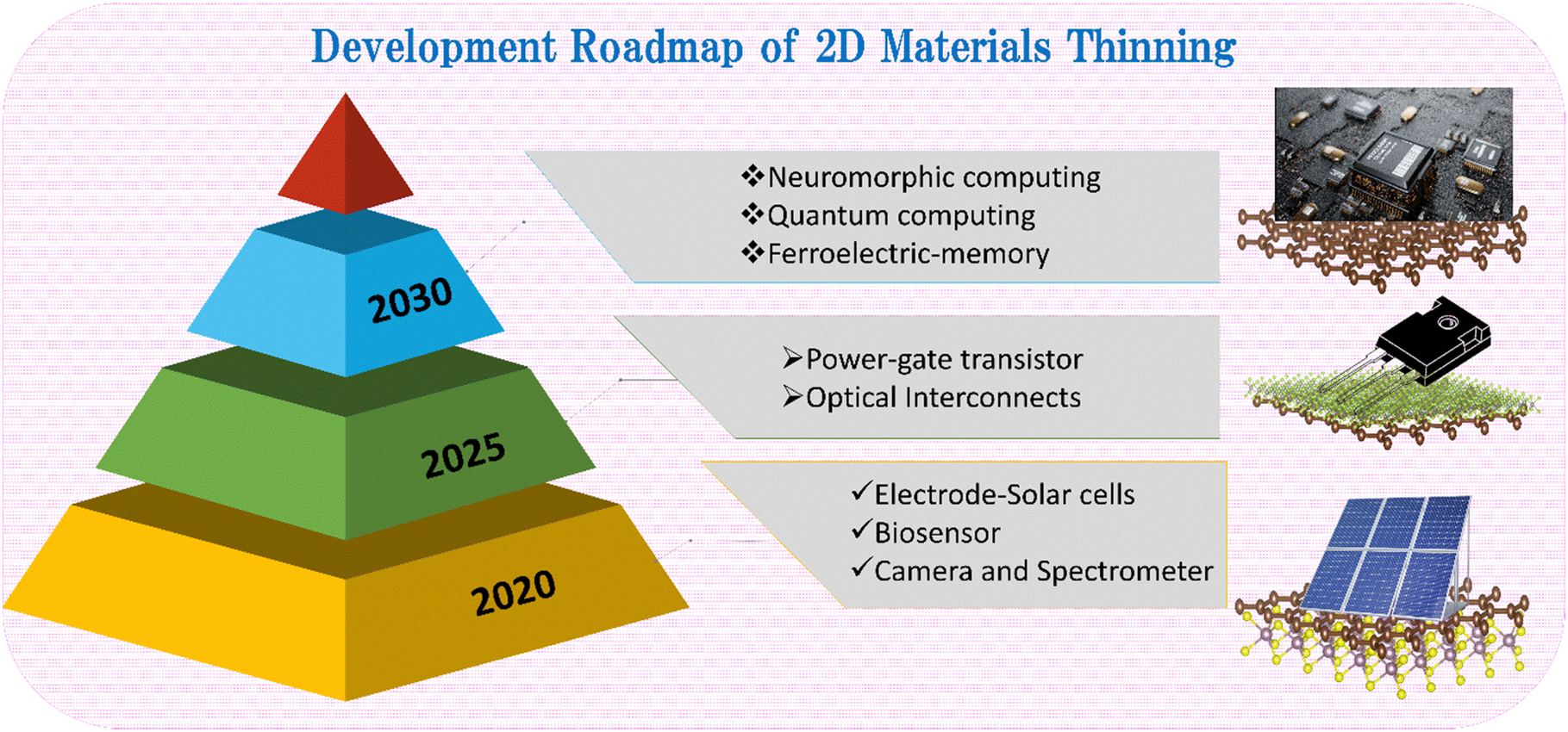 | ||
| Fig. 20 Prospective development roadmap of thinned 2D materials for integrated modern electronics/optoelectronics. | ||
To visualize the development roadmap of this research direction, the top–down layer-by-layer thinning strategies were expressed as a knight that is atomically slicing the topmost thinned layer of 2D materials, which can be applied to artificially grown multilayer materials to date (Fig. 21). The intention is to guide readers in better understanding and visualizing advanced layer-by-layer thinning technologies at the atomic scale through the depiction of a slicing knight. This image serves as a representative symbol, illustrating the impact of chemical bonds and interactions (such as covalent bonding, ionic bonding, and π bonding). Importantly, it aligns seamlessly with the chemical-related scopes. The combination of top–down thinning strategies and 2D materials is poised to drive innovations across multidisciplinary industries, revolutionizing electronics, photonics, energy harvesting and storage, and beyond. As research and development in this field continue to progress, these layer-by-layer thinning strategies hold significant potential to unlock new transformative technologies with superior performance, efficiency, and versatility.
 | ||
| Fig. 21 A knight is atomically slicing the topmost thinned layer of 2D materials as represented by the advanced top–down layer-by-layer thinning strategies at the atomic scale applicable to artificially representative grown multilayer materials. | ||
Author contributions
CRediT: Phuong V. Pham conceptualization, funding acquisition, project administration, supervision, writing-original draft, writing–review & editing. The-Hung Mai writing-original draft, writing–review & editing; Huy-Binh Do review & editing; M. Vasundhara review & editing; Van-Huy Nguyen review & editing; Trieu Nguyen review & editing; Hao Van Bui review & editing; Van-Duong Dao review & editing; Ram K. Gupta review & editing; Vinoth Kumar Ponnusamy writing–review & editing, funding acquisition, supervision; Jin-Hong Park funding acquisition, supervision, writing–review & editing, supervision.Conflicts of interest
The authors declare that they have no known competing financial interests or personal relationships that could have appeared to influence the work reported in this paper.Acknowledgements
The authors acknowledge the support from the National Science and Technology Council, Taiwan (Grant No.: NSTC-112-2112-M-110-004-MY3), the Research Center for Precision Environmental Medicine, Kaohsiung Medical University, Kaohsiung, Taiwan from The Featured Areas Research Center Program within the framework of the Higher Education Sprout Project by the Ministry of Education (MOE) in Taiwan and by Kaohsiung Medical University Research Center Grant (KMUTC113A01), and the grant MOST-110-2113-M-037-009 from the Ministry of Science and Technology, Taiwan. This research was supported by the National Research Foundation of Korea (NRF) (2022M3F3A2A01072215, 2021R1A2C2010026). This work was also supported by the Technology Innovation Program (RS-2023-00235609, Proposal of 3D DRAM development direction from the process development of vertical stacked cell transistors) funded by the Ministry of Trade, Industry & Energy (MOTIE, Korea) (1415187471).References
- G. V. Resta, T. Agarwal, D. Lin, I. P. Radu, F. Catthoor, P. E. Gaillardon and G. De Micheli, Sci. Rep, 2017, 7, 1–9 CrossRef PubMed.
- G. E. Moore, Electronics, 1965, 38, 114–117 Search PubMed.
- J. Bardeen and W. H. Brattain, Phys. Rev., 1948, 74, 230–231 CrossRef.
- H.-B.-R. Lee and S. Kim, Chem. Mater., 2023, 35, 4117–4119 CrossRef CAS.
- R. Quhe, L. Xu, S. Liu, C. Yang, Y. Wang, H. Li, J. Yang, Q. Li, B. Shi, Y. Li, Y. Pan, X. Sun, J. Li, M. Weng, H. Zhang, Y. Guo, L. Xu, H. Tang, J. Dong, J. Yang, Z. Zhang, M. Lei, F. Pan and J. Lu, Phys. Rep., 2021, 938, 1–72 CrossRef CAS.
- D. E. Nikonov and I. A. Young, Proc. IEEE, 2013, 101, 2498–2533 CAS.
- A. C. Ferrari, F. Bonaccorso, V. Fal’ko, K. S. Novoselov, S. Roche, P. Bøggild, S. Borini, F. H. L. Koppens, V. Palermo, N. Pugno, J. A. Garrido, R. Sordan, A. Bianco, L. Ballerini, M. Prato, E. Lidorikis, J. Kivioja, C. Marinelli, T. Ryhänen, A. Morpurgo, J. N. Coleman, V. Nicolosi, L. Colombo, A. Fert, M. Garcia-Hernandez, A. Bachtold, G. F. Schneider, F. Guinea, C. Dekker, M. Barbone, Z. Sun, C. Galiotis, A. N. Grigorenko, G. Konstantatos, A. Kis, M. Katsnelson, L. Vandersypen, A. Loiseau, V. Morandi, D. Neumaier, E. Treossi, V. Pellegrini, M. Polini, A. Tredicucci, G. M. Williams, B. Hee Hong, J. H. Ahn, J. Min Kim, H. Zirath, B. J. VanWees, H. Van DerZant, L. Occhipinti, A. DiMatteo, I. A. Kinloch, T. Seyller, E. Quesnel, X. Feng, K. Teo, N. Rupesinghe, P. Hakonen, S. R. T. Neil, Q. Tannock, T. Löfwander and J. Kinaret, Nanoscale, 2015, 7, 4598–4810 RSC.
- A. Singh Dahiya, A. Zumeit, A. Christou and R. Dahiya, Adv. Electron. Mater., 2022, 8, 2200098 CrossRef.
- D. I. Kim, J. W. Lee, R. H. Jeong and J. H. Boo, Sci. Rep., 2022, 12, 1–10 CrossRef PubMed.
- W. Jiang, S. Lee, K. Zhao, K. Lee, H. Han, J. W. Oh, H. Lee, H. Kim, C. M. Koo and C. Park, ACS Nano, 2022, 16, 9203–9213 CrossRef CAS PubMed.
- K. S. Novoselov, A. K. Geim, S. V. Morozov, D. Jiang, Y. Zhang, S. V. Dubonos, I. V. Grigorieva and A. A. Firsov, Science., 2004, 306, 666–669 CrossRef CAS PubMed.
- K. S. Novoselov, A. K. Geim, S. V. Morozov, D. Jiang, M. I. Katsnelson, I. V. Grigorieva, S. V. Dubonos and A. A. Firsov, Nature, 2005, 438, 197–200 CrossRef CAS PubMed.
- V. P. Pham, Y. W. Jo, J. S. Oh, S. M. Kim, J. W. Park, S. H. Kim, M. S. Jhon and G. Y. Yeom, Jpn. J. Appl. Phys., 2013, 52, 075102 CrossRef.
- P. V. Pham, R. Soc. Open Sci., 2018, 5, 1–6 Search PubMed.
- V. P. Pham, K. H. Kim, M. H. Jeon, S. H. Lee, K. N. Kim and G. Y. Yeom, Carbon N. Y., 2015, 95, 664–671 CrossRef CAS.
- V. P. Pham, A. Mishra and G. Young Yeom, RSC Adv., 2017, 7, 16104–16108 RSC.
- K. N. Kim, V. P. Pham and G. Y. Yeom, ECS J. Solid State Sci. Technol., 2015, 4, N5095–N5097 CrossRef CAS.
- V. P. Pham, D. S. Kim, K. S. Kim, J. W. Park, K. C. Yang, S. H. Lee, G. Y. Yeom and K. N. Kim, Sci. Adv. Mater., 2016, 8, 884–890 CrossRef CAS.
- V. P. Pham, M. T. Nguyen, J. W. Park, S. S. Kwak, D. H. T. Nguyen, M. K. Mun, H. D. Phan, D. S. Kim, K. H. Kim, N. E. Lee and G. Y. Yeom, 2D Mater., 2017, 4, 025049 CrossRef.
- V. P. Pham, K. N. Kim, M. H. Jeon, K. S. Kim and G. Y. Yeom, Nanoscale, 2014, 6, 15301–15308 RSC.
- P. V. Pham, ACS Omega, 2018, 3, 8036–8041 CrossRef CAS PubMed.
- V. P. Pham, H. S. Jang, D. Whang and J. Y. Choi, Chem. Soc. Rev., 2017, 46, 6276–6300 RSC.
- P. V. Pham, C, 2018, 4, 34 Search PubMed.
- P. V. Pham, The New Etching Technologies of Graphene Surfaces, IntechOpen, 2020 DOI:10.5772/intechopen.92627.
- P. Pham, P. Goel, S. Kumar and K. Yadav, 21st Century Surface Science - a Handbook, IntechOpen. 2020 DOI:10.5772/intechopen.87891.
- K. A. A. Min-Dianey, T. K. Le, J. R. Choi and P. V. Pham, Nanomaterials, 2021, 11, 816 CrossRef CAS PubMed.
- K. A. A. Min-Dianey, T. K. Le, A. Qadir, N. L. P. M’bouana, M. Malik, S. W. Kim, J. R. Choi and P. V. Pham, Nanomaterials, 2021, 11, 2934 CrossRef CAS PubMed.
- U. Farooq, K. A. A. Min-Dianey, P. Rajagopalan, M. Malik, D. M. Kongnine, J. R. Choi and P. V. Pham, Nanomaterials, 2022, 12, 712 CrossRef CAS PubMed.
- M. A. Iqbal, M. Malik, W. Shahid, W. Ahmad, K. A. A. Min-Dianey and P. V. Pham, Plasmonic 2D Materials: Overview, Advancements, Future Prospects and Functional Applications, 2022, vol. 3 DOI:10.5772/intechopen.101580.
- P. V. Pham, S. Chanakya Bodepudi, K. Shehzad, Y. Liu, Y. Xu, B. Yu and X. Duan, Chem. Rev., 2022, 122, 6514–6613 CrossRef CAS PubMed.
- Y. Zheng, H. Wang, S. Hou, D. Xia, Y. Zheng, H. Wang, S. Hou and D. Xia, Adv. Mater. Technol., 2017, 2, 1600237 CrossRef.
- J. M. Pietryga, K. K. Zhuravlev, M. Whitehead, V. I. Klimov and R. D. Schaller, Phys. Rev. Lett., 2008, 101, 217401 CrossRef PubMed.
- P. V. Pham, T.-H. Mai, H.-B. Do, V. K. Ponnusamy and F.-C. Chuang, Micromachines, 2023, 14, 1060 CrossRef PubMed.
- A. A. Balandin, Nat. Mater., 2011, 10, 569–581 CrossRef CAS PubMed.
- A. K. Geim, Science., 2009, 324, 1530–1534 CrossRef CAS PubMed.
- Y. Hernandez, V. Nicolosi, M. Lotya, F. M. Blighe, Z. Sun, S. De, I. T. McGovern, B. Holland, M. Byrne, Y. K. Gun’ko, J. J. Boland, P. Niraj, G. Duesberg, S. Krishnamurthy, R. Goodhue, J. Hutchison, V. Scardaci, A. C. Ferrari and J. N. Coleman, Nat. Nanotechnol., 2008, 3, 563–568 CrossRef CAS PubMed.
- B. Jayasena and S. Subbiah, Nanoscale Res. Lett., 2011, 6, 1–7 CrossRef PubMed.
- J. Chen, M. Duan and G. Chen, J. Mater. Chem., 2012, 22, 19625–19628 RSC.
- T. Khac Le, A. The-Hung Mai, M. Aamir Iqbal, D. Vernardou, V.-D. Dao, V. Kumar Ponnusamy, G. Chandra Sekhar Rout and P. VPham, RSC Adv., 2023, 13, 31273–31291 RSC.
- J. Li, M. Chen, A. Samad, H. Dong, A. Ray, J. Zhang, X. Jiang, U. Schwingenschlögl, J. Domke, C. Chen, Y. Han, T. Fritz, R. S. Ruoff, B. Tian and X. Zhang, Nat. Mater., 2022, 21, 740–747 CrossRef CAS PubMed.
- L. Wang, X. Xu, L. Zhang, R. Qiao, M. Wu, Z. Wang, S. Zhang, J. Liang, Z. Zhang, Z. Zhang, W. Chen, X. Xie, J. Zong, Y. Shan, Y. Guo, M. Willinger, H. Wu, Q. Li, W. Wang, P. Gao, S. Wu, Y. Zhang, Y. Jiang, D. Yu, E. Wang, X. Bai, Z. J. Wang, F. Ding and K. Liu, Nature, 2019, 570, 91–95 CrossRef CAS PubMed.
- T. Li, W. Guo, L. Ma, W. Li, Z. Yu, Z. Han, S. Gao, L. Liu, D. Fan, Z. Wang, Y. Yang, W. Lin, Z. Luo, X. Chen, N. Dai, X. Tu, D. Pan, Y. Yao, P. Wang, Y. Nie, J. Wang, Y. Shi and X. Wang, Nat. Nanotechnol., 2021, 16, 1201–1207 CrossRef CAS PubMed.
- P. V. Pham, Nature-Inspired Self-Cleaning Surfaces Nanotechnology Era, 2023, vol. 6, p. 120 DOI:10.5772/INTECHOPEN.106087.
- T. He, Z. Wang, F. Zhong, H. Fang, P. Wang and W. Hu, Adv. Mater. Technol., 2019, 4, 1900064 CrossRef CAS.
- M. Marchena, F. Wagner, T. Arliguie, B. Zhu, B. Johnson, M. Fernández, T. L. Chen, T. Chang, R. Lee, V. Pruneri and P. Mazumder, 2D Mater., 2018, 5, 035022 CrossRef.
- N. Basu, R. Kumar, D. Manikandan, M. Ghosh Dastidar, P. Hedge, P. K. Nayak and V. P. Bhallamudi, RSC Adv., 2023, 13, 16241–16247 RSC.
- J. T. Mlack, P. Masih Das, G. Danda, Y. C. Chou, C. H. Naylor, Z. Lin, N. P. López, T. Zhang, M. Terrones, A. T. C. Johnson and M. Drndic, Sci. Rep, 2017, 7, 1–8 CrossRef PubMed.
- C. Xie, X. Zhang, K. Ruan, Z. Shao, S. S. Dhaliwal, L. Wang, Q. Zhang, X. Zhang and J. Jie, J. Mater. Chem. A, 2013, 1, 15348–15354 RSC.
- S. Li, M. Zeng, Y. Huang, R. Zhan, J. Chen, N. Xu, J. She and S. Deng, J. Micromech. Microeng., 2018, 28, 085001 CrossRef.
- H. Agarwal, K. Nowakowski, A. Forrer, A. Principi, R. Bertini, S. Batlle-Porro, A. Reserbat-Plantey, P. Prasad, L. Vistoli, K. Watanabe, T. Taniguchi, A. Bachtold, G. Scalari, R. Krishna Kumar and F. H. L. Koppens, Nat. Photonics, 2023, 17, 1047–1053 CrossRef CAS.
- Y. Zhang, T. T. Tang, C. Girit, Z. Hao, M. C. Martin, A. Zettl, M. F. Crommie, Y. R. Shen and F. Wang, Nature, 2009, 459, 820–823 CrossRef CAS PubMed.
- A. Dey, A. Chroneos, N. S. J. Braithwaite, R. P. Gandhiraman and S. Krishnamurthy, Appl. Phys. Rev., 2016, 3, 021301 Search PubMed.
- H. Conrads and M. Schmidt, Plasma Sources Sci. Technol., 2000, 9, 441–454 CrossRef CAS.
- V. M. Donnelly and A. Kornblit, J. Vac. Sci. Technol. A, 2013, 31, 050825 CrossRef.
- R. J. Gasvoda, A. W. Van DeSteeg, R. Bhowmick, E. A. Hudson and S. Agarwal, ACS Appl. Mater. Interfaces, 2017, 9, 31067–31075 CrossRef CAS PubMed.
- F. Fracassi, R. D’Agostino, R. Lamendola, A. Filippo, C. Rapisarda and P. Vasquez, J. Electrochem. Soc., 1996, 143, 701–707 CrossRef CAS.
- J. W. Coburn and H. F. Winters, Appl. Surf. Sci., 1985, 22–23, 63–71 CAS.
- J. A. Bondur, J. Vac. Sci. Technol., 1976, 13, 1023–1029 CrossRef CAS.
- L. Xie, T. X. Zhou, R. J. Stöhr and A. Yacoby, Adv. Mater., 2018, 30, 1705501 CrossRef PubMed.
- H. Al-Mumen, F. Rao, W. Li and L. Dong, Nano-Micro Lett., 2014, 6, 116–124 CrossRef.
- F. A. Khan and I. Adesida, Appl. Phys. Lett., 1999, 75, 2268–2270 CrossRef CAS.
- J. J. Wang, E. S. Lambers, S. J. Pearton, M. Ostling, C. M. Zetterling, J. M. Grow, F. Ren and R. J. Shul, Solid. State. Electron., 1998, 42, 2283–2288 CrossRef CAS.
- B. Li, L. Cao and J. H. Zhao, Appl. Phys. Lett., 1998, 73, 653–655 CrossRef CAS.
- G. Robert Bigras, X. Glad, L. Vandsburger, C. Charpin, P. Levesque, R. Martel and L. Stafford, Carbon N. Y., 2019, 144, 532–539 CrossRef.
- L. Zhang, S. Feng, S. Xiao, G. Shen, X. Zhang, H. Nan, X. Gu and K. (Ken)Ostrikov, Appl. Surf. Sci., 2018, 441, 639–646 CrossRef CAS.
- J. Jia, S. K. Jang, S. Lai, J. Xu, Y. J. Choi, J. H. Park and S. Lee, ACS Nano, 2015, 9, 8729–8736 CrossRef CAS PubMed.
- C. G. N. Lee, K. J. Kanarik and R. A. Gottscho, J. Phys. D. Appl. Phys., 2014, 47, 273001 CrossRef.
- K. J. Kanarik, T. Lill, E. A. Hudson, S. Sriraman, S. Tan, J. Marks, V. Vahedi and R. A. Gottscho, J. Vac. Sci. Technol. A, 2015, 33, 020802 CrossRef.
- R. C. Longo, A. Ranjan and P. L. G. Ventzek, ACS Appl. Nano Mater., 2020, 3, 5189–5202 CrossRef CAS.
- S. Yasmeen, S. W. Ryu, S. H. Lee and H. B. R. Lee, Adv. Mater. Technol., 2022, 2200876, 2200876 Search PubMed.
- K. C. Chen, T. W. Chu, C. R. Wu, S. C. Lee and S. Y. Lin, 2D Mater., 2017, 4, 034001 CrossRef.
- A. Fischer, A. Routzahn, S. M. George and T. Lill, J. Vac. Sci. Technol. A Vacuum, Surfaces, Film., 2021, 39, 30801 CrossRef CAS.
- J. Soares, A. U. Mane, D. Choudhury, S. Letourneau, S. M. Hues, J. W. Elam and E. Graugnard, Chem. Mater., 2023, 35, 927–936 CrossRef CAS PubMed.
- K. S. Kim, Y. J. Ji, Y. Nam, K. H. Kim, E. Singh, J. Y. Lee and G. Y. Yeom, Sci. Rep., 2017, 7, 1–9 CrossRef PubMed.
- W. S. Lim, Y. Y. Kim, H. Kim, S. Jang, N. Kwon, B. J. Park, J. H. Ahn, I. Chung, B. H. Hong and G. Y. Yeom, Carbon N. Y., 2012, 50, 429–435 CrossRef CAS.
- K. S. Kim, K. H. Kim, J. E. Kang, J. H. Lee, Y. J. Ji and G. Y. Yeom, ACS Appl. Electron. Mater., 2022, 4, 3794–3800 CrossRef CAS.
- K. S. Kim, K. H. Kim, Y. J. Ji and G. Y. Yeom, ECS Trans., 2018, 86, 69 CrossRef.
- Z. Ma, C. Prawoto, Z. Ahmed, Y. Xiao, L. Zhang, C. Zhou and M. Chan, J. Mater. Chem. C, 2019, 7, 6273–6278 RSC.
- H. Kwon, S. W. Seo, T. G. Kim, E. S. Lee, P. T. Lanh, S. Yang, S. Ryu and J. W. Kim, ACS Nano, 2016, 10, 8723–8731 CrossRef CAS PubMed.
- Y. You, J. Park and J. Kim, ECS J. Solid State Sci. Technol., 2023, 12, 075009 CrossRef.
- Y. Rho, J. Pei, L. Wang, Z. Su, M. Eliceiri and C. P. Grigoropoulos, ACS Appl. Mater. Interfaces, 2019, 11, 39385–39393 CrossRef CAS PubMed.
- Y. Zhou, Q. Bao, B. Varghese, L. A. L. Tang, C. K. Tan, C. H. Sow and K. P. Loh, Adv. Mater., 2010, 22, 67–71 CrossRef CAS PubMed.
- D. W. Li, Y. S. Zhou, X. Huang, L. Jiang, J.-F. Silvain and Y. F. Lu, Nanoscale, 2015, 7, 3651–3659 RSC.
- V. A. Ermakov, A. V. Alaferdov, A. R. Vaz, E. Perim, P. A. S. Autreto, R. Paupitz, D. S. Galvao and S. A. Moshkalev, Sci. Rep., 2015, 5, 1–9 Search PubMed.
- A. Castellanos-Gomez, M. Barkelid, A. M. Goossens, V. E. Calado, H. S. J. Van DerZant and G. A. Steele, Nano Lett., 2012, 12, 3187–3192 CrossRef CAS PubMed.
- J. Lu, J. Wu, A. Carvalho, A. Ziletti, H. Liu, J. Tan, Y. Chen, A. H. Castro Neto, B. Özyilmaz and C. H. Sow, ACS Nano, 2015, 9, 10411–10421 CrossRef CAS PubMed.
- A. V. Zaretski, H. Moetazedi, C. Kong, E. J. Sawyer, S. Savagatrup, E. Valle, T. F. O’Connor, A. D. Printz and D. J. Lipomi, Nanotechnology, 2015, 26, 045301 CrossRef CAS PubMed.
- J. Kim, H. Park, J. B. Hannon, S. W. Bedell, K. Fogel, D. K. Sadana and C. Dimitrakopoulos, Science., 2013, 342, 833–836 CrossRef CAS PubMed.
- J. Shim, S. H. Bae, W. Kong, D. Lee, K. Qiao, D. Nezich, Y. J. Park, R. Zhao, S. Sundaram, X. Li, H. Yeon, C. Choi, H. Kum, R. Yue, G. Zhou, Y. Ou, K. Lee, J. Moodera, X. Zhao, J. H. Ahn, C. Hinkle, A. Ougazzaden and J. Kim, Science, 2018, 362, 665–670 CrossRef CAS PubMed.
- J. Li, H. Ji, X. Zhang, X. Wang, Z. Jin, D. Wang and L. J. Wan, Chem. Commun., 2014, 50, 11012–11015 RSC.
- W. Li, G. Cheng, Y. Liang, B. Tian, X. Liang, L. Peng, A. R. Hight Walker, D. J. Gundlach and N. V. Nguyen, Carbon N. Y., 2016, 99, 348–353 CrossRef CAS.
- H. K. Ng, D. Xiang, A. Suwardi, G. Hu, K. Yang, Y. Zhao, T. Liu, Z. Cao, H. Liu, S. Li, J. Cao, Q. Zhu, Z. Dong, C. K. I. Tan, D. Chi, C. W. Qiu, K. Hippalgaonkar, G. Eda, M. Yang and J. Wu, Nat. Electron., 2022, 5, 489–496 CrossRef CAS.
- L. Chu, H. Schmidt, J. Pu, S. Wang, B. Özyilmaz, T. Takenobu and G. Eda, Sci. Rep., 2014, 4, 1–6 Search PubMed.
- M. S. Cao, X. X. Wang, W. Q. Cao and J. Yuan, J. Mater. Chem. C, 2015, 3, 6589–6599 RSC.
- X. Li, T. Yang, Y. Yang, J. Zhu, L. Li, F. E. Alam, X. Li, K. Wang, H. Cheng, C.-T. Lin, Y. Fang and H. Zhu, Adv. Funct. Mater., 2016, 26, 1322–1329 CrossRef CAS.
- S. Bertolazzi, J. Brivio and A. Kis, ACS Nano, 2011, 5, 9703–9709 CrossRef CAS PubMed.
- T. Chekke, R. Narzary, S. Ngadong, B. Satpati, S. Bayan and U. Das, Sens. Actuators, A, 2023, 349, 114076 CrossRef CAS.
- X. Zeng, Z. Ding, C. Ma, L. Wu, J. Liu, L. Chen, D. G. Ivey and W. Wei, ACS Appl. Mater. Interfaces, 2016, 8, 18841–18848 CrossRef CAS PubMed.
- E. O. Polat, H. B. Uzlu, O. Balci, N. Kakenov, E. Kovalska and C. Kocabas, ACS Photonics, 2016, 3, 964–971 CrossRef CAS.
- S. Sarma, P. Mbule and S. C. Ray, Appl. Surf. Sci., 2019, 479, 1118–1123 CrossRef CAS.
- W. Zhang, Q. Wang, Y. Chen, Z. Wang and A. T. S. Wee, 2D Mater., 2016, 3, 022001 CrossRef.
- Y. Hwang, T. Kim and N. Shin, ACS Appl. Nano Mater, 2021, 4, 12034–12042 CrossRef CAS.
- M. Alamri, M. Gong, B. Cook, R. Goul and J. Z. Wu, ACS Appl. Mater. Interfaces, 2019, 11, 33390–33398 CrossRef CAS PubMed.
- D. Geng, B. Wu, Y. Guo, B. Luo, Y. Xue, J. Chen, G. Yu and Y. Liu, J. Am. Chem. Soc., 2013, 135, 6431–6434 CrossRef CAS PubMed.
- J. W. Park, S. K. Jang, D. H. Kang, D. S. Kim, M. H. Jeon, W. O. Lee, K. S. Kim, S. J. Lee, J. H. Park, K. N. Kim and G. Y. Yeom, J. Mater. Chem. C, 2017, 5, 10888–10893 RSC.
- J. W. Park, D. S. Kim, M. K. Mun, W. O. Lee, K. S. Kim and G. Y. Yeom, J. Phys. D. Appl. Phys., 2017, 50, 254007 CrossRef.
- K. S. Kim, K. H. Kim, Y. Nam, J. Jeon, S. Yim, E. Singh, J. Y. Lee, S. J. Lee, Y. S. Jung, G. Y. Yeom and D. W. Kim, ACS Appl. Mater. Interfaces, 2017, 9, 11967–11976 CrossRef CAS PubMed.
- K. S. Kim, Y. J. Ji, K. H. Kim, S. Choi, D. H. Kang, K. Heo, S. Cho, S. Yim, S. Lee, J. H. Park, Y. S. Jung and G. Y. Yeom, Nat. Commun., 2019, 10, 1–10 CrossRef PubMed.
- K. Xu, D. Chen, F. Yang, Z. Wang, L. Yin, F. Wang, R. Cheng, K. Liu, J. Xiong, Q. Liu and J. He, Nano Lett., 2017, 17, 1065–1070 CrossRef CAS PubMed.
- H. Park, G. H. Shin, K. J. Lee and S. Y. Choi, Nanoscale, 2018, 10, 15205–15212 RSC.
- Y. Huang, Y. H. Pan, R. Yang, L. H. Bao, L. Meng, H. L. Luo, Y. Q. Cai, G. D. Liu, W. J. Zhao, Z. Zhou, L. M. Wu, Z. L. Zhu, M. Huang, L. W. Liu, L. Liu, P. Cheng, K. H. Wu, S. B. Tian, C. Z. Gu, Y. G. Shi, Y. F. Guo, Z. G. Cheng, J. P. Hu, L. Zhao, G. H. Yang, E. Sutter, P. Sutter, Y. L. Wang, W. Ji, X. J. Zhou and H. J. Gao, Nat. Commun., 2020, 11, 1–9 CrossRef PubMed.
- L. Guan, B. Xing, X. Niu, D. Wang, Y. Yu, S. Zhang, X. Yan, Y. Wang and J. Sha, Chem. Commun., 2018, 54, 595–598 RSC.
- E. Cho, A. T. Nguyen, S. Lim, J. Cho, J. Song, S. Kwon and D. W. Kim, J. Phys. D. Appl. Phys., 2023, 56, 325101 CrossRef.
- Y. Yao and C. P. Wong, Carbon N. Y., 2012, 50, 5203–5209 CrossRef CAS.
- Y. Y. Stehle, X. Sang, R. R. Unocic, D. Voylov, R. K. Jackson, S. Smirnov and I. Vlassiouk, Nano Lett., 2017, 17, 7306–7314 CrossRef CAS PubMed.
- A. Felten, A. Eckmann, J. J. Pireaux, R. Krupke and C. Casiraghi, Nanotechnology, 2013, 24, 355705 CrossRef CAS PubMed.
- F. Ghasemi, A. Abdollahi and S. Mohajerzadeh, ACS Omega, 2019, 4, 19693–19704 CrossRef CAS PubMed.
- Y. Y. Kim, W. S. Lim, J. B. Park and G. Y. Yeom, J. Electrochem. Soc., 2011, 158, D710 CrossRef CAS.
- T. Z. Lin, B. T. Kang, M. H. Jeon, C. Huffman, J. H. Jeon, S. J. Lee, W. Han, J. Y. Lee, S. H. Lee, G. Y. Yeom and K. N. Kim, ACS Appl. Mater. Interfaces, 2015, 7, 15892–15897 CrossRef CAS PubMed.
- Y. Liu, X. Duan, H. J. Shin, S. Park, Y. Huang and X. Duan, Nature, 2021, 591, 43–53 CrossRef CAS PubMed.
- Q. Qiu and Z. Huang, Adv. Mater., 2021, 33, 2008126 CrossRef CAS PubMed.
- Z. Sun, A. Martinez and F. Wang, Nat. Photonics, 2016, 10, 227–238 CrossRef CAS.
- X. Yang, S. Tang, G. Ding, X. Xie, M. Jiang and F. Huang, Nanotechnology, 2012, 23, 025704 CrossRef PubMed.
- J. Bai, X. Zhong, S. Jiang, Y. Huang and X. Duan, Nat. Nanotechnol., 2010, 5, 190–194 CrossRef CAS PubMed.
- M. Wojtaszek, N. Tombros, A. Caretta, P. H. M. VanLoosdrecht and B. J. VanWees, J. Appl. Phys., 2011, 110, 063715 CrossRef.
- G. Kalita, L. Qi, Y. Namba, K. Wakita and M. Umeno, Mater. Lett., 2011, 65, 1569–1572 CrossRef CAS.
- Y. Zhang, K. Ma, C. Zhao, W. Hong, C. Nie, Z. J. Qiu and S. Wang, ACS Nano, 2021, 15, 4405–4415 CrossRef CAS PubMed.
- C. Wang, Q. Wu, Y. Ding, Z. Cai, S. Xiao, X. Zhang, H. Nan and X. Gu, Appl. Phys. Express, 2022, 16, 015003 CrossRef.
- S. Wi, H. Kim, M. Chen, H. Nam, L. J. Guo, E. Meyhofer and X. Liang, ACS Nano, 2014, 8, 5270–5281 CrossRef CAS PubMed.
- J. An, X. Zhao, Y. Zhang, M. Liu, J. Yuan, X. Sun, Z. Zhang, B. Wang, S. Li and D. Li, Adv. Funct. Mater., 2022, 32, 2110119 CrossRef CAS.
- S. Yu, X. Wu, Y. Wang, X. Guo, L. Tong, S. L. Yu, X. Q. Wu, Y. P. Wang, X. Guo and L. M. Tong, Adv. Mater., 2017, 29, 1606128 CrossRef PubMed.
- O. DelPozo-Zamudio, A. Genco, S. Schwarz, F. Withers, P. M. Walker, T. Godde, R. C. Schofield, A. P. Rooney, E. Prestat, K. Watanabe, T. Taniguchi, C. Clark, S. J. Haigh, D. N. Krizhanovskii, K. S. Novoselov and A. I. Tartakovskii, 2D Mater., 2020, 7, 031006 CrossRef CAS.
- J. Wang, J. Han, X. Chen and X. Wang, InfoMat, 2019, 1, 33–53 CrossRef CAS.
- L. Wang, W. Liu, Y. Zhang, Z. H. Zhang, S. Tiam Tan, X. Yi, G. Wang, X. Sun, H. Zhu and H. Volkan Demir, Nano Energy, 2015, 12, 419–436 CrossRef CAS.
- T. H. Han, Y. Lee, M. R. Choi, S. H. Woo, S. H. Bae, B. H. Hong, J. H. Ahn and T. W. Lee, Nat. Photonics, 2012, 6, 105–110 CrossRef CAS.
- C. Kim, T. Phan Nguyen, Q. VanLe, J.-M. Jeon, H. Won Jang and S. Young Kim, Adv. Funct. Mater., 2015, 25, 4512–4519 CrossRef CAS.
- E. O. Polat and C. Kocabas, Nano Lett., 2013, 13, 5851–5857 CrossRef CAS PubMed.
- Z. B. Liu, M. Feng, W. S. Jiang, W. Xin, P. Wang, Q. W. Sheng, Y. G. Liu, D. N. Wang, W. Y. Zhou and J. G. Tian, Laser Phys. Lett., 2013, 10, 065901 CrossRef CAS.
- Y. Wu, Y. M. Lin, A. A. Bol, K. A. Jenkins, F. Xia, D. B. Farmer, Y. Zhu and P. Avouris, Nature, 2011, 472, 74–78 CrossRef CAS PubMed.
- M. Kim, P. Kang, J. Leem and S. W. Nam, Nanoscale, 2017, 9, 4058–4065 RSC.
- K. Y. Thai, I. Park, B. J. Kim, A. T. Hoang, Y. Na, C. U. Park, Y. Chae and J. H. Ahn, ACS Nano, 2021, 15, 12836–12846 CrossRef CAS PubMed.
- F. Xue, L. Chen, L. Wang, Y. Pang, J. Chen, C. Zhang and Z. L. Wang, Adv. Funct. Mater., 2016, 26, 2104–2109 CrossRef CAS.
- S. Wu, Y. Chen, X. Wang, H. Jiao, Q. Zhao, X. Huang, X. Tai, Y. Zhou, H. Chen, X. Wang, S. Huang, H. Yan, T. Lin, H. Shen, W. Hu, X. Meng, J. Chu and J. Wang, Nat. Commun., 2022, 13, 1–9 Search PubMed.
- J. Xu, Y. J. Song, J. H. Park and S. Lee, Solid. State. Electron., 2018, 144, 86–89 CrossRef CAS.
- W. Zhu, M. N. Yogeesh, S. Yang, S. H. Aldave, J. S. Kim, S. Sonde, L. Tao, N. Lu and D. Akinwande, Nano Lett., 2015, 15, 1883–1890 CrossRef CAS PubMed.
- Z. Wang, Y. Chen, P. Wu, J. Ye, M. Peng, Y. Yan, F. Zhong, T. He, Y. Wang, M. Xu, K. Zhang, Z. Hu, Q. Li, L. Zhang, F. Wang and P. Wang, Infrared Phys. Technol., 2020, 106, 103272 CrossRef CAS.
- C. Jung, S. M. Kim, H. Moon, G. Han, J. Kwon, Y. K. Hong, I. Omkaram, Y. Yoon, S. Kim and J. Park, Sci. Rep, 2015, 5, 1–9 Search PubMed.
- B. Chamlagain, Q. Li, N. J. Ghimire, H. J. Chuang, M. M. Perera, H. Tu, Y. Xu, M. Pan, D. Xaio, J. Yan, D. Mandrus and Z. Zhou, ACS Nano, 2014, 8, 5079–5088 CrossRef CAS PubMed.
- L. Huang, B. Dong, X. Guo, Y. Chang, N. Chen, X. Huang, W. Liao, C. Zhu, H. Wang, C. Lee and K. W. Ang, ACS Nano, 2019, 13, 913–921 CrossRef CAS PubMed.
- X. Yu, P. Yu, D. Wu, B. Singh, Q. Zeng, H. Lin, W. Zhou, J. Lin, K. Suenaga, Z. Liu and Q. J. Wang, Nat. Commun., 2018, 9, 1–9 CrossRef PubMed.
- X. Zhou, X. Hu, J. Yu, S. Liu, Z. Shu, Q. Zhang, H. Li, Y. Ma, H. Xu, T. Zhai, X. Zhou, X. Z. Hu, J. Yu, Z. W. Shu, Q. Zhang, H. Q. Li, Y. Ma, T. Y. Zhai, S. Liu and H. Xu, Adv. Funct. Mater., 2018, 28, 1706587 CrossRef.
- C. H. Lee, G. H. Lee, A. M. Van DerZande, W. Chen, Y. Li, M. Han, X. Cui, G. Arefe, C. Nuckolls, T. F. Heinz, J. Guo, J. Hone and P. Kim, Nat. Nanotechnol., 2014, 9, 676–681 CrossRef CAS PubMed.
- M. Massicotte, P. Schmidt, F. Vialla, K. Watanabe, T. Taniguchi, K. J. Tielrooij and F. H. L. Koppens, Nat. Commun., 2016, 7, 1–7 Search PubMed.
- J. H. Gosling, O. Makarovsky, F. Wang, N. D. Cottam, M. T. Greenaway, A. Patanè, R. D. Wildman, C. J. Tuck, L. Turyanska and T. M. Fromhold, Commun. Phys., 2021, 4, 1–8 CrossRef.
- M. S. Choi, A. Nipane, B. S. Y. Kim, M. E. Ziffer, I. Datta, A. Borah, Y. Jung, B. Kim, D. Rhodes, A. Jindal, Z. A. Lamport, M. Lee, A. Zangiabadi, M. N. Nair, T. Taniguchi, K. Watanabe, I. Kymissis, A. N. Pasupathy, M. Lipson, X. Zhu, W. J. Yoo, J. Hone and J. T. Teherani, Nat. Electron., 2021, 4, 731–739 CrossRef CAS.
- L. Banszerus, M. Schmitz, S. Engels, J. Dauber, M. Oellers, F. Haupt, K. Watanabe, T. Taniguchi, B. Beschoten and C. Stampfer, Sci. Adv, 2015, 1, e1500222 CrossRef PubMed.
- M. Y. Han, B. Özyilmaz, Y. Zhang and P. Kim, Phys. Rev. Lett., 2007, 98, 206805 CrossRef PubMed.
- T. Ohta, A. Bostwick, T. Seyller, K. Horn and E. Rotenberg, Science., 2006, 313, 951–954 CrossRef CAS PubMed.
- X. Wang and H. Dai, Nat. Chem., 2010, 2, 661–665 CrossRef CAS PubMed.
- J. Meyer, S. Hamwi, M. Kröger, W. Kowalsky, T. Riedl and A. Kahn, Adv. Mater., 2012, 24, 5408–5427 CrossRef CAS PubMed.
- Y. Sui and J. Appenzeller, Nano Lett., 2009, 9, 2973–2977 CrossRef CAS PubMed.
- D. Bischof, M. Kahl and M. Michler, Opt. Mater. Express, 2021, 11, 1185–1195 CrossRef.
- G. A. Shafeev, E. D. Obraztsova and S. M. Pimenov, Mater. Sci. Eng., B, 1997, 46, 129–132 CrossRef.
- M. A. Bissett, A. G. Hattle, A. J. Marsden, I. A. Kinloch and R. A. W. Dryfe, ACS Omega, 2017, 2, 738–745 CrossRef CAS PubMed.
- R. Tao, X. Qu, Z. Wang, F. Li, L. Yang, J. Li, D. Wang, K. Zheng and M. Dong, J. Mater. Sci. Technol., 2022, 119, 61–68 CrossRef CAS.
- D. Wang, Y. Wang, X. Chen, Y. Zhu, K. Zhan, H. Cheng and X. Wang, Nanoscale, 2016, 8, 4107–4112 RSC.
- Y. Sha, S. Xiao, X. Zhang, F. Qin and X. Gu, Appl. Surf. Sci., 2017, 411, 182–188 CrossRef CAS.
- V. Karthik Nagareddy, T. J. Octon, N. J. Townsend, S. Russo, M. F. Craciun, C. David Wright, V. K. Nagareddy, T. J. Octon, N. J. Townsend, S. Russo, M. F. Craciun and C. D. Wright, Adv. Funct. Mater., 2018, 28, 1804434 CrossRef.
- C. Pei, X. Li, H. Fan, J. Wang, H. You, P. Yang, C. Wei, S. Wang, X. Shen and H. Li, ACS Appl. Nano Mater, 2020, 3, 4218–4230 CrossRef CAS.
- G. Lee, J. Y. Lee, G. H. Lee and J. Kim, J. Mater. Chem. C, 2016, 4, 6234–6239 RSC.
- C. J. Banas, M. Aman Uddin, J. Park, B.-C. Tran-Khac, R. M. White, F. W. DelRio and K.-H. Chung, Nanotechnology, 2019, 30, 275302 CrossRef PubMed.
- S. Huang, J. Li, J. Fang, H. Ding, W. Huang, X. Zhao and Y. Zheng, ACS Appl. Mater. Interfaces, 2021, 13, 58966–58973 CrossRef CAS PubMed.
- J. Pei, X. Gai, J. Yang, X. Wang, Z. Yu, D. Y. Choi, B. Luther-Davies and Y. Lu, Nat. Commun., 2016, 7, 1–8 Search PubMed.
- T. Das, D. Seo, J. Eun Seo, J. Chang, T. Das, D. Seo, J. E. Seo and J. Chang, Adv. Electron. Mater., 2020, 6, 2000008 CrossRef CAS.
- P. V. Pham, 21st Century Nanostructured Materials - Physics, Chemistry, Classification, and Emerging Applications in Industry, Biomedicine, and Agriculture, 2022, vol. 17 DOI:10.5772/intechopen.94802.
- X. Huang, C. Liu and P. Zhou, 2D Mater. Appl., 2022, 6, 1–19 CrossRef.
- X. Song, J. Hu and H. Zeng, J. Mater. Chem. C, 2013, 1, 2952–2969 RSC.
- H. Sun, J. Dong, F. Liu and F. Ding, Mater. Today, 2021, 42, 192–213 CrossRef CAS.
- M. A. Iqbal, N. Anwar, M. Malik, M. Al-Bahrani, M. R. Islam, J. R. Choi, P. V. Pham and X. Liu, Adv. Mater. Interfaces, 2023, 10, 2202208 CrossRef CAS.
- S. Manzhos, C. C. Chueh, G. Giorgi, T. Kubo, G. Saianand, J. Lüder, P. Sonar and M. Ihara, J. Phys. Chem. Lett., 2021, 12, 4638–4657 CrossRef CAS PubMed.
- S. Bellani, A. Bartolotta, A. Agresti, G. Calogero, G. Grancini, A. DiCarlo, E. Kymakis and F. Bonaccorso, Chem. Soc. Rev., 2021, 50, 11870–11965 RSC.
- G. R. Bhimanapati, Z. Lin, V. Meunier, Y. Jung, J. Cha, S. Das, D. Xiao, Y. Son, M. S. Strano, V. R. Cooper, L. Liang, S. G. Louie, E. Ringe, W. Zhou, S. S. Kim, R. R. Naik, B. G. Sumpter, H. Terrones, F. Xia, Y. Wang, J. Zhu, D. Akinwande, N. Alem, J. A. Schuller, R. E. Schaak, M. Terrones and J. A. Robinson, ACS Nano, 2015, 9, 11509–11539 CrossRef CAS PubMed.
- H. M. Li, D. Lee, D. Qu, X. Liu, J. Ryu, A. Seabaugh and W. J. Yoo, Nat. Commun., 2015, 6, 1–9 CAS.
- Y. Du, H. Liu, A. T. Neal, M. Si and P. D. Ye, IEEE Electron Device Lett., 2013, 34, 1328–1330 CAS.
- J. D. Lin, C. Han, F. Wang, R. Wang, D. Xiang, S. Qin, X. A. Zhang, L. Wang, H. Zhang, A. T. S. Wee and W. Chen, ACS Nano, 2014, 8, 5323–5329 CrossRef CAS PubMed.
- S. Tongay, J. Zhou, C. Ataca, J. Liu, J. S. Kang, T. S. Matthews, L. You, J. Li, J. C. Grossman and J. Wu, Nano Lett., 2013, 13, 2831–2836 CrossRef CAS PubMed.
- H. Puliyalil and U. Cvelbar, Nanomaterials, 2016, 6, 108 CrossRef PubMed.
- J. E. Andrew, P. E. Dyer, D. Forster and P. H. Key, Appl. Phys. Lett., 1983, 43, 717–719 CrossRef CAS.
- O. Joubert, J. Pelletier and Y. Arnal, J. Appl. Phys., 1989, 65, 5096–5100 CrossRef.
- P. E. Dyer and R. J. Farley, Appl. Phys. Lett., 1990, 57, 765–767 CrossRef CAS.
- D. J. DaSilva and D. S. Rosa, ACS Appl. Polym. Mater., 2022, 4, 7162–7172 CrossRef CAS.
- E. Wohlfart, J. P. Fernández-Blázquez, E. Knoche, A. Bello, E. Pérez, E. Arzt and A. DelCampo, Macromolecules, 2010, 43, 9908–9917 CrossRef CAS.
- A. Bès, M. Koo, T. L. Phan, A. Lacoste and J. Pelletier, Plasma Process. Polym., 2018, 15, 1800038 CrossRef.
- G. Greczynski, D. Primetzhofer and L. Hultman, Appl. Surf. Sci., 2018, 436, 102–110 CrossRef CAS.
- M. Naguib, O. Mashtalir, J. Carle, V. Presser, J. Lu, L. Hultman, Y. Gogotsi and M. W. Barsoum, ACS Nano, 2012, 6, 1322–1331 CrossRef CAS PubMed.
- J. Halim, S. Kota, M. R. Lukatskaya, M. Naguib, M. Q. Zhao, E. J. Moon, J. Pitock, J. Nanda, S. J. May, Y. Gogotsi and M. W. Barsoum, Adv. Funct. Mater., 2016, 26, 3118–3127 CrossRef CAS.
- J. Yang, M. Naguib, M. Ghidiu, L. M. Pan, J. Gu, J. Nanda, J. Halim, Y. Gogotsi and M. W. Barsoum, J. Am. Ceram. Soc., 2016, 99, 660–666 CrossRef CAS.
- B. Soundiraraju and B. K. George, ACS Nano, 2017, 11, 8892–8900 CrossRef CAS PubMed.
- B. Anasori, Y. Xie, M. Beidaghi, J. Lu, B. C. Hosler, L. Hultman, P. R. C. Kent, Y. Gogotsi and M. W. Barsoum, ACS Nano, 2015, 9, 9507–9516 CrossRef CAS PubMed.
- B. Shi, P. Wang, J. Feng, C. Xue, G. Yang, Q. Liao, M. Zhang, X. Zhang, W. Wen and J. Wu, Nano-Micro Lett., 2023, 15, 1–18 CrossRef PubMed.
- H. C. Lin, Y. C. Lee, C. C. Lin, Y. L. Ho, D. Xing, M. H. Chen, B. W. Lin, L. Y. Chen, C. W. Chen and J. J. Delaunay, Nanoscale, 2022, 14, 10075–10081 RSC.
- K. G. Brooks and M. K. Nazeeruddin, Adv. Energy Mater., 2021, 11, 2101149 CrossRef CAS.
- L. Zhang, M. T. Hörantner, W. Zhang, Q. Yan and H. J. Snaith, Sol. Energy Mater. Sol. Cells, 2017, 160, 193–202 CrossRef CAS.
- X. Xiao, C. Bao, Y. Fang, J. Dai, B. R. Ecker, C. Wang, Y. Lin, S. Tang, Y. Liu, Y. Deng, X. Zheng, Y. Gao, X. Cheng Zeng and J. Huang, Adv. Mater., 2018, 30, 1705176 CrossRef PubMed.
- D. A. Scrymgeour, T. L. Sounart, N. C. Simmons and J. W. P. Hsu, J. Appl. Phys., 2007, 101, 014316 CrossRef.
- D. Eisert, W. Braun, S. Kuhn, J. Koeth and A. Forchel, Microelectron. Eng., 1999, 46, 179–181 CrossRef CAS.
- W. R. Hendren, A. Murphy, P. Evans, D. O’Connor, G. A. Wurtz, A. V. Zayats, R. Atkinson and R. J. Pollard, J. Phys. Condens. Matter, 2008, 20, 362203 CrossRef.
- E. A. Ogryzlo, D. E. Ibbotson, D. L. Flamm and J. A. Mucha, J. Appl. Phys., 1990, 67, 3115–3120 CrossRef CAS.
- F. Schäffel, J. H. Warner, A. Bachmatiuk, B. Rellinghaus, B. Büchner, L. Schultz and M. H. Rümmeli, Nano Res., 2009, 2, 695–705 CrossRef.
- D. A. Stocker, I. D. Goepfert, E. F. Schubert, K. S. Boutros and J. M. Redwing, J. Electrochem. Soc., 2000, 147, 763 CrossRef CAS.
- R. Wang, J. Wang, H. Gong, Z. Luo, D. Zhan, Z. Shen and J. T. L. Thong, Small, 2012, 8, 2515–2523 CrossRef CAS PubMed.
- L. L. Janavicius, J. A. Michaels, C. Chan, D. J. Sievers and X. Li, Appl. Phys. Rev., 2023, 10, 011409 CAS.
- J. Kim, D. H. Lee, J. H. Kim and S. H. Choi, ACS Appl. Mater. Interfaces, 2015, 7, 24242–24246 CrossRef CAS PubMed.
- H. Han, Z. Huang and W. Lee, Nano Today, 2014, 9, 271–304 CrossRef CAS.
- J. J. Huang, C. S. Huang, J. Y. Wang, P. Y. Chang, C. N. Chen and S. L. Ou, Appl. Phys. A Mater. Sci. Process, 2022, 128, 1–12 CrossRef.
- Z. Wu, J. Qi, W. Wang, Z. Zeng and Q. He, J. Mater. Chem. A, 2021, 9, 18793–18817 RSC.
- R. Raccichini, A. Varzi, S. Passerini and B. Scrosati, Nat. Mater., 2014, 14, 271–279 CrossRef PubMed.
- V. Panwar, P. S. Chauhan, S. Kumar, R. Tripathi and A. Misra, ACS Energy Lett., 2023, 8, 1510–1519 CrossRef CAS.
- R. Han, F. Liu, X. Wang, M. Huang, W. Li, Y. Yamauchi, X. Sun and Z. Huang, J. Mater. Chem. A, 2020, 8, 14384–14399 RSC.
- M. M. Rahman, M. R. Hossen, I. Alam, M. H. Rahman, O. Faruk, M. Nurbas, M. M. Rahman and M. M. R. Khan, J. Alloys Compd., 2023, 947, 169471 CrossRef CAS.
- M. Tomy, A. Ambika Rajappan, V. M. Vimuna and X. Thankappan Suryabai, Energy Fuels, 2021, 35, 19881–19900 CrossRef CAS.
- A. F. Khan, M. P. Down, G. C. Smith, C. W. Foster and C. E. Banks, J. Mater. Chem. A, 2017, 5, 4103–4113 RSC.
- F. Bonaccorso, Z. Sun, T. Hasan and A. C. Ferrari, Nat. Photonics, 2010, 4, 611–622 CrossRef CAS.
- P. Kienitz, A. Bablich, R. Bornemann, M. Müller, F. Thiel and P. H. Bolívar, Nano Lett., 2023, 23, 5535–5540 CrossRef CAS PubMed.
- D. Yue, X. Ju, T. Hu, X. Rong, X. Liu, X. Liu, H. K. Ng, D. Chi, X. Wang and J. Wu, Nanoscale, 2023, 15, 4940–4950 RSC.
- Z. Xie, G. Li, S. Xia, C. Liu, S. Zhang, Z. Zeng, X. Liu, D. Flandre, Z. Fan, L. Liao and X. Zou, Nano Lett., 2023, 23, 6664–6672 CrossRef CAS PubMed.
- B. Tan, Y. Wu, F. Gao, H. Yang, Y. Hu, H. Shang, X. Zhang, J. Zhang, Z. Li, Y. Fu, D. Jia, Y. Zhou, H. Xiao and P. Hu, ACS Appl. Mater. Interfaces, 2022, 14, 16453–16461 CrossRef CAS PubMed.
- S. Ngamprapawat, J. Kawase, T. Nishimura, K. Watanabe, T. Taniguchi and K. Nagashio, Adv. Electron. Mater., 2023, 9, 2300083 CrossRef CAS.
- G. Jiang, H. Tian, X. F. Wang, T. Hirtz, F. Wu, Y. C. Qiao, G. Y. Gou, Y. H. Wei, J. M. Yang, S. Yang, Y. Yang and T. L. Ren, Nanoscale Adv., 2019, 1, 4745–4754 RSC.
- A. Pal, S. Zhang, T. Chavan, K. Agashiwala, C.-H. Yeh, W. Cao and K. Banerjee, Adv. Mater., 2023, 35, 2109894 CrossRef CAS PubMed.
- Z. Fan, J. Qu, T. Wang, A.-H. Nath Jaiswal, M. Liu, S. Shahi, H. Hu, H. Wang, Y. Sun, L. Chen, M. Er Pam, S. Li and K.-W. Ang, Neuromorphic Comput. Eng, 2022, 2, 022001 CrossRef.
- X. Jin, Y. Y. Zhang and S. Du, Fundam. Res., 2023, 3, 322–331 CrossRef CAS.
- L. Jin, H. Wang, R. Cao, K. Khan, A. K. Tareen, S. Wageh, A. A. Al-Ghamdi, S. Li, D. Li, Y. Zhang and H. Zhang, APL Mater, 2022, 10, 060903 CrossRef CAS.
- J. Xu, L. Chen, Y. W. Dai, Q. Cao, Q. Q. Sun, S. J. Ding, H. Zhu and D. W. Zhang, Sci. Adv., 2017, 3, e1602246 CrossRef PubMed.
- Q. Zhang, C. Liu and P. Zhou, iScience, 2023, 26, 106673 CrossRef CAS PubMed.
- I. A. Calafell, J. D. Cox, M. Radonjić, J. R. M. Saavedra, F. J. García de Abajo, L. A. Rozema and P. Walther, Quantum Inf., 2019, 5, 1–7 CrossRef.
- A. Lipatov, P. Sharma, A. Gruverman and A. Sinitskii, ACS Nano, 2015, 9, 8089–8098 CrossRef CAS PubMed.
Footnote |
| † These authors contributed equally to this work. |
| This journal is © The Royal Society of Chemistry 2024 |