Tailoring van der Waals interactions in ultra-thin two dimensional metal–organic frameworks (MOFs) for photoconductive applications†
Received
27th August 2024
, Accepted 26th September 2024
First published on 27th September 2024
Abstract
The diverse structural tunability of 2-dimensional π-stacked layered metal–organic frameworks (2D MOFs) enables the control of charge carrier mobility to achieve specific photoconductive characteristics. This study demonstrates the potential of various theoretical methodologies and frameworks in establishing a correlation between structure and functionality for such purposes. Through a focus on the archetypal Ni3(HITP)2 2D MOF, we examine the impact of quantum confinement and stacking fault defects on the absorption spectra using our recently-developed Frenkel–Holstein Hamiltonian. Specifically, the relationship between optical properties and number of layer units along the π-stacking direction is discussed. We employ Marcus rate theory to evaluate vertical carrier mobility subject to inter-layer proximity and different crystal packing which affect van der Waals interactions between layers. The insights presented in this research can inform the development of guidelines for enhancing photoconductive properties in 2D MOF nanosheets.
1. Introduction
Besides their distinctive conductive properties,1,2 two-dimensional (2D) metal–organic frameworks (MOFs) have garnered increased research interest recently due to their potential application as photocatalytic materials exhibiting tunable electronic and optical characteristics.3–5 As shown in Fig. 1(a), in 2D MOFs atoms are arranged into layers held together by in-plane covalent or coordinative bonds. These layers are subsequently arranged in the out-of-plane direction with relatively weak van der Waals (vdW) interactions, resulting in the formation of parallel 1D channels. This specific architecture facilitates bulk exfoliation and nanosheet manufacturing, even down to a single layer.6,7 Consequently, in comparison to their 3D bulk counterparts, 2D MOFs present ultra-thin thickness,6 large surface area8 and effective charge separation,9 all of which facilitate the efficient transfer of captured energy to external acceptors, thereby enhancing the photocatalytic performance of the material.10 Indeed, 2D MOFs may exhibit non-zero band gaps,11i.e., semiconductive behaviour, as shown by their intrinsic temperature dependent electrical conductivity.11,12
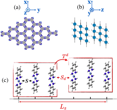 |
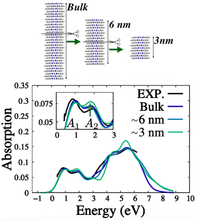
| | Fig. 1 (a) Crystal structure of the 2D layered Ni3(HITP)2 (HITP = 2, 3, 6, 7, 10, 11-hexaiminotriphenylene) MOF with hexagonal 1D channels along the π-stacking direction. (b) Schematic diagram of the layer–layer displacement defect (stacking fault) along the π-stacking as in reference Foster et al.13 (c) A representative reduced model of Ni3(HITP)2 employed in this work with parameters S and Sd monitoring inter-layer and stacking fault spacings between units, respectively. Finally, Lz controls the vertical π-stacking length. | |
This semiconductive characteristic was recently corroborated by our computational analysis of electronic properties14 for the archetypal layered MOF Ni3(HITP)2 (HITP = 2, 3, 6, 7, 10, 11-hexaiminotriphenylene).11,15,16 Through ab initio molecular dynamics (AIMD) simulations and subsequent band structure calculations, we have shown that finite temperature induces a competition between the openings of direct and indirect band gaps in 2D layered MOFs.14
Hence, generation and recombination rates of photo-induced electron–hole (e–h) pairs in 2D MOFs depend on both the wavelength-dependent absorption rate and the energy conservation balance at the Fermi level. Nevertheless, understanding structure–property relationships in 2D layered MOFs is essentially in its early stages. Atomistic-level insights created by theoretical studies can provide guidelines to significantly improve the photoconductive properties of these intriguing systems. Indeed, AIMD methods can provide complementary insights while also explicitly accounting for the finite temperature.17 One of the questions to be addressed, before any compact device implementation, is how the spatial confinement affects charge transport and optical properties in ultra-thin 2D MOFs.18,19 Another critical inquiry involves the correlation between charge transport and crystal packing along the stacking direction as well as whether the vdW interactions can be enhanced by tuning the crystal packing of the layered architecture. In this context, we have very recently shown20 that the inter-layer overlap of the electronic wavefunctions and thus the transfer integral (t) in 2D MOFs is intricately dependent on both the inter-layer distance and orientation of the layers and scales with the reorganization energy (λ). Herein, using the archetypal Ni3(HITP)2 2D MOF, we elaborate on how spatial confinement and inter-layer proximity21 along the π-stacking may be tailored in order to modulate optical properties and vertical mobility in ultra-thin 2D MOFs. The theoretical model is summarized in the next section. Section 3 introduces the stacking fault Hamiltonian. Section 4 provides the results and the associated discussions on absorption spectra and mobility.
2. The model
To study the effect of confinement and stacking fault defects13 on optical properties and carrier mobility of 2D MOFs, we design a model of Ni3(HITP)2 system as demonstrated in Fig. 1(c). This model consists of a linear array of N + 1 secondary building units (SBUs)20,22 along the non-covalent π-stacking direction. The length of this stack of SBUs is defined as Lz while S and Sd parameters corresponds to the inter-layer spacing between the two SBU units and to the stacking fault spacing, respectively. Due to the optical invariance with respect to the relative in plane sliding, the triphenylene organic linkers in each unit were truncated to benzene rings.20 Given the ability in molybdenum disulfide to tune the band gap as a function of the number of layers and to detect the light at different wavelengths,23 we first investigate how the optical response may vary with the thickness Lz. For this purpose, we use the Holstein Hamiltonian24–26 that has been recently employed to study the absorption spectrum of Ni3(HITP)2.20 We have shown that this Hamiltonian, containing the phonon coupling at finite temperature, can provide an accurate description of the carrier hopping between building units of 2D frameworks.
3. The Hamiltonian
The Hamiltonian is comprised of four terms:| | | H = HJ + HT + HPOL + HD | (1) |
where the first term includes the vibronic coupling (the Frenkel term), the second term accounts for electron and hole transfers and the third term includes the energies of the polaronic states and their associated vibronic couplings (more details can be found in reference dell’Angelo et al.20). The last term takes into account the stacking fault defect as represented in Fig. 1(c):The first term of eqn (2) accounts for electron and hole transfers at the stacking fault: (3)where tde and tdh represent the transfer integrals which arise from HOMO–HOMO and LUMO–LUMO interactions between nearest neighbour SBUs and decay exponentially with distance Sd. The second term in eqn (2) includes the energies of the polaronic states and their associated vibronic couplings:
| | 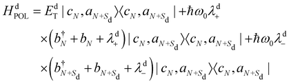 | (4) |
where the EdT energy is a function of the separation (Sd) between the hole on monomer N and the electron on monomer N + Sd, whereas the second and the third term of eqn (4) monitor the local vibrational coupling quantified by the dimensionless λd(+/−) factors. The effective coupling between units is provided by the interference of the charge transfer T with the exciton Coulomb coupling JCoul and can be either constructive or destructive, according to the expression:27where| |  | (6) |
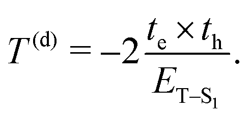
ET–S1 in eqn (6) is the difference between the charge transfer energy and the energy of the S0 → S1 electronic transition. te and th stand for electron and hole transfer integrals and monitor the strength of the interaction and the ease of charge transfer within a dimer made of two consecutive units (the apex d referring to the interaction at the stacking fault). They are obtained by calculating the dimer Hamiltonian in the atomic orbital basis from the Roothaan equation:where S is the overlap matrix and the matrix C corresponds to the supramolecular orbitals of the dimer. Eqn (6) implies a two-step super exchange process28 in which the exciton moves between two consecutive units via a virtual charge transfer state. Since in our model we assume ET–S1 > 0, T can be positive or negative depending on the sign of the product tp = te × th. Hence, the relative sign between te and th controls the J- and H-like photophysical properties in layered MOF aggregates. Here, J stands for induced red shift29 whereas H stands for induced blue shift30 as a result of the aggregation.
4. Results and discussion
In order to elucidate the correlation between spatial confinement and properties in thin 2D-MOF, this section is divided into two segments: the initial one underscores the optical characteristics, while the subsequent one delves into the vertical mobility within the stacking model.
4.1. Modulation of the absorbance spectrum
4.1.1. Effect of the quantum confinement on the spectra.
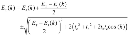
Fig. 2 shows the absorption spectrum of a bulk model of Ni3(HITP)2 comprised of a 1D stack of N = 30 SBU monomers in navy blue against the experimental spectrum in black where the Holstein Hamiltonian reproduces the position and intensity of peaks in the experimental spectrum. The Hamiltonian also provides us with means to study the effect of quantum confinement along Lz by monitoring the ratio between the first two vibronic peaks of the spectra A1 and A2 relative to 0–0/0–1 ratio of the monomer.20 It has been already reported25,31 that the ratio of the first two peaks of the absorption spectrum (A1/A2) depends on the nature of the coulombic coupling. In particular, this ratio increases with the magnitude of the intermolecular coupling in J-aggregates (JCoul < 0, red shift) and decreases in H-aggregates (JCoul > 0, blue shift). After careful inspection of the convergence with respect to the number of vibrational quanta for Frenkel and charge transfer states (see Fig. 3), the onset in Fig. 2 shows that by decreasing Lz to 6 and 3 nm the A1/A2 ratio decreases which is an H-aggregate feature. This indicates how photophysical properties of 2D MOFs may be tailored by progressive exfoliation.
 |
| | Fig. 2 Calculated absorption spectra as a result of exfoliating Ni3(HITP)2 along the vertical dimension Lz. Provided the experimental15 inter-layer spacing S = 3.3 Å (see Fig. 1b), the illustrated quantum confinement models correspond to Lz = 5.94 nm and Lz = 2.97 nm and are comprised of 18 and 9 units, respectively. The experimental profile is taken from reference Sheberla et al.11 The remainder of the parameters are JCoul = 1100, th = 910, te = 875 and ET–S1 = 1400 cm−1. | |
 |
| | Fig. 3 Provided the onset of the spectra in Fig. 2, these profiles show the convergence with respect to the number of vibrational quanta for Frenkel and charge transfer states as a result of exfoliating Ni3(HITP)2 along the vertical dimension (a) Lz = 5.94 nm and (b) Lz = 2.97 nm. The converged profiles (nvib = 7) were then used for generating Fig. 2. | |
4.1.2. Tailoring the absorption peaks.
Additionally, the A1/A2 ratio may be further refined via engineering the energy difference ET–S1. Fig. 4 shows how the optical response of the model Ni3(HITP)2 evolves in two different regimes: R, the resonance regime where ET ≈ ES1, and qR, the quasi-resonance regime where ET ≈ 1.5ES1. All parameters used in these simulations are reported in Table S1 in the ESI.† The left panel of Fig. 4 displays a notable linear increase in the A1/A2 ratio as a function of the charge transfer product tp, inducing a J-like feature31 in both regimes. Although the resonance regime shows an overall higher A1/A2 ratio than the quasi-resonance regime, these ratios are closer at small transfer integral values, in particular when tp ∼ 2.5 × 105 cm−1. At tp > 5 × 105 cm−1 an increasing divergence of the ratios calculated at two regimes is observed, meaning that the J-aggregation signature may be modulated according to both the interaction strength between consecutive SBUs and energy difference ET–S1. The implication is the potential use of the absorption spectrum to screen different aggregates for photoconductive purposes. It is therefore useful to map the energy values spanned by the absorption spectra as a function of tp, as illustrated in the right panel of Fig. 4. Here, one can recognize the regions of the highest and lowest intensities (dark regions) in both regimes. However, a closer look reveals that the spectrum in the R regime is slightly red shifted with respect to the one in the qR regime.
 |
| | Fig. 4 The simulated A1/A2 ratio (left panel) and the absorption energy and intensity (right panel) at the quasi-resonance (qR) and resonance (R) regimes as a function of the transfer integral product tp = th × te. The full set of parameters is reported in the ESI,† Table S1. | |
4.2. Vertical mobility
4.2.1. Effect of the quantum confinement on the carrier mobility.
Vertical confinement and proximity effects,21 manifested in the parameters Lz and S, may also be employed to manipulate vertical charge mobility in ultra-thin 2D MOFs and hence engineer desired photoconductive properties. It is thus insightful to first establish the relationship between the thickness of the film and the resistivity (ρ)32,33 when a progressive vertical exfoliation reaches the quantum well (QW) limit (see the ESI,† Fig. S1). By definition, as long as the exfoliation does not alter carriers motion in any of the three dimensions, ρ displays bulk characteristics. At certain Lz value, the strong 2D confinement starts altering carriers flow. As a result, ρ starts increasing because of the decreasing relaxation time (i.e., the average time between two consecutive scattering events). However, when the progressive exfoliation reaches the point where the De Broglie wavelength of the bound carrier (typically in the range λω ∼ 1–10 nm (ref. 34)) becomes comparable to the QW thickness, a dramatic drop in resistivity is observed and quantum phenomena begin to dominate physical properties of the material.35
Vertical quantum confinement increases absorption efficiency, which results from the strongly bound elect€(e)–hole(h) paired quasiparticles due to the weaker dielectric screening in a nanometer thickness.36,37 Further, the enhanced exciton binding energy exerts a significant influence on both the energy transport and optical characteristics within the material. Insights into exciton dynamics may be obtained from the momentum (k)–energy (E) dispersion relation. For a given k, the JCoul/T mixing can be studied by applying the dispersion relation38
| |  | (8) |
where the exciton delocalization energy
EJ(
k) is evaluated as a function of the coulombic interaction
39| | EJ(k) = ES1+ 2JCoul![[thin space (1/6-em)]](https://www.rsc.org/images/entities/char_2009.gif) cos(k) cos(k) | (9) |
where
ES1 corresponds to the energy of the S
0 → S
1 electronic transition. In
eqn (9), the wave vector
k is in 1/
S units and takes on the values
k = 0, ±2π/
N, ±4π/
N,…, π and only the nodeless exciton with wave vector
k = 0 is optically allowed. Hence, depending on the negative (positive) sign of
JCoul, the transition energy is lower (higher) than the monomeric transition energy, resulting in aggregation induced red (blue) shift in the optical absorption spectrum of
J(H)-aggregates.
Fig. 5 shows for
Lz = 5.94 nm in the slide and eclipsed configurations how the
k–
E dispersion varies by progressively decreasing the energy difference
ET–S1, from qR
1 to qR
3, until the
R regime is reached (values are reported in Table S2, ESI
†). While the eclipsed configuration is barely affected by the
ET–S1 progression, in the slide situation the spectra shift from blue to red. However, it is worth mentioning that these profiles may change in the presence of defects, which may trap carriers in localized states, thus effectively modulating the resistance of the material.
 |
| | Fig. 5 Momentum(k)–exciton (E) dispersion profiles as a function of the energy difference ET–S1. Left (right) panel corresponds to the slide (eclipsed) configuration between consecutive monomers. The full set of parameters is reported in the ESI,† Table S2. | |
4.2.2. Tailoring the vertical mobility.
Now, we turn our attention to evaluating the charge carrier mobility along the vertical dimension in ultra-thin Ni3(HITP)2 subjected to progressive exfoliation. Assuming that an external electric field along the π-stacking direction is applied to our model Ni3(HITP)2, as depicted in Fig. 6, charge carriers move with a wavelength λω while experiencing the periodic potential variation due to the periodic arrangement of the atoms along the stacking direction. The net force on the carrier is due to F = Fext + Fint, where Fint corresponds to the crystal field. The response to in Ni3(HITP)2 is notably influenced by the metal d bands, as the latter plays a prime role in forming the direct/indirect band gap via the s–d and p–d couplings,40,41 thus establishing photoconductive properties of the material. Provided the expression for the effective mass 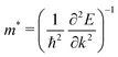 , the crystal field is already taken into account in the Bloch's wavefunction and the crystal momentum p = ħk responds only to Fext, i.e. as if it was a free particle (more details can be found in the ESI,† Section S1). However, as displayed in Fig. 6, the physical confinement caused by the medium automatically restricts the oscillatory period of the wavefunction. This means that the round trip phase of the latter must be a multiple integer of 2π, according to the standing condition:
| | | 2kr = Q·2π Q = 1, 2, 3… | (10) |
where the factor 2 on the LHS denotes the completion of a round trip phase kr. If we consider the three orthogonal components of the wavevector k ≡ (kx, ky, kz), as a result of the spatial confinement λqω = 2Lz/q, the k component along the stacking direction can assume a set of values as:| | 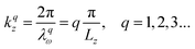 | (11) |
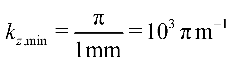
Then, one can calculate the minimum and the maximum values of kz using Lz or S in the denominator, respectively. For instance, if we assume a device with Lz = 1 mm, the smallest kz value corresponds to  . On the other hand, considering the experimental15 value of S = 3.3 Å in Ni3(HITP)2,
  , which means that the number of allowed states along kz may vary as 106 orders of magnitude (in steps of 103 π m−1) between the edges of the first Brillouin zone, see Fig. 7. Progressive exfoliation of Lz down to the QW limit, i.e. region (c) in Fig. S1 in the ESI,† leads to a dramatic discretization of the allowed states along kz. For example, if Lz reaches ≈1 nm, the number of allowed states along z reduces to only 3 with
  ,
,  , and
, and  . As a result, as presented in Table 1, the densities of states become directly dependent on Lz, see the ESI,† Section S1 for the corresponding derivations.
 |
| | Fig. 6 Representation of a carrier moving along the π-stacking direction and experiencing the crystal field (Fint) which varies as a function of the inter-layer spacing S. The carrier wavelength ranges between λω,min = 2S and λω,max = 2Lz. | |
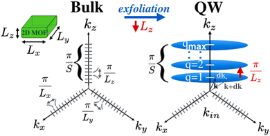 |
| | Fig. 7 Representation of the allowed states in the Ni3(HITP)2 thin layer in the k-space. By exfoliating Lz, the kz step increases such that the number of allowed states along z becomes highly discretized. Yet, in the xy-plane the number of allowed states kin = kx × ky remains very large. The blue planes correspond to the space of allowed states (i.e., no states are permitted between them). | |
Table 1 Expressions for the bulk and QW densities in k and Ec (conduction band) spaces (for derivations see the ESI, Section S1)
For photoconductive engineering purposes, Fig. S3 (ESI†) shows how the discretization along kz can be used to tailor the effective band gap34,42Eeffg as a function of Lz. Assuming the same value for m* in both conduction and valence bands, the relationship can be formulated as:
| |  | (12) |
Eqn (12) can be used as a guideline for evaluating the threshold
Lz values below which quantum mechanical effects would dictate the photoconductive properties of the material. Nevertheless, under
operando conditions, it is not possible to attain the desired photoconductive attributes solely by adjusting
Lz. In such scenarios, the carrier mobility is also affected by imperfections. These imperfections can be categorized into two main types (or combinations of both): point imperfections resulting from atoms being out of place within the 2D structure due to temperature effects (commonly referred to as defects), and larger dislocations caused by the relative lateral movement between layers.
4.2.3. Gauging the hopping rate.
If the Ni3(HITP)2 stacking was well-ordered and free from any imperfections, the carrier wavefunctions would be delocalized over many units and a through-band transport could be attained. Yet, even in well-ordered chains of conjugated units, macroscopic transport is governed by hopping mechanism due to presence of imperfections and defects.43 Ours and others works has firmly established that layer-layer displacements in 2D MOFs are a major source of imperfection.13,14,44 Specifically, very recently, we have shown20 the effect of the relative sliding between layers and their corresponding geometrical changes on the absorption spectra of 2D MOFs as they can be gauged by evaluating transfer integrals (t) and reorganization energy (λ), respectively. Briefly, the geometrical changes in the units of our Ni3(HITP)2 model, when going from neutral to excited/charged states, can be gauged by calculating an effective Huang–Rhys factor λeff (in the harmonic approximation):45| |  | (13) |
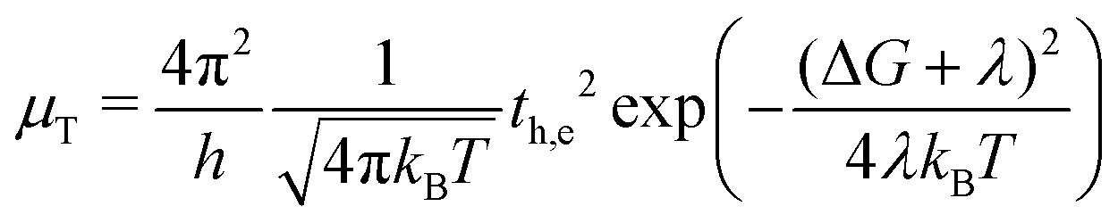
where ωi represents the frequency of the normal mode i while Ri is the projection of the displacements between equilibrium geometries of the neutral and radical-cation or radical-anion states (hereafter, for the sake of brevity, we refer to λeff simply as the reorganization energy λ). Eventually, whether a band-like or hopping transport mechanism is operative, charge-transport characteristics depend on both λ and t parameters.46,47 Since Marcus rate theory suggests that the inter-unit charge transfer and the hopping rate can be determined by these parameters,48–51 it serves as a beneficial tool for investigating carrier mobility in 2D MOF nanosheets. Here, we evaluate vertical hopping rates μT along the stacking direction according to the expression:| |  | (14) |
where th,e may represent the carrier tunneling rate and the exponential factor rules the activation energy or the energy barrier for the charge transfer between two consecutive units. With the aim of evaluating the effect of inter-layer proximity on the carrier hopping along the π-stacking direction in the nanosheet, we maintain the same value of Lz = 5.94 nm as in Fig. 2 except that now we vary the total number of units N hence changing the inter-layer distance S. Fig. 8 illustrates the increasing trend for electron mobility with decreasing S at three different temperatures of T1 = 290 K, T2 = 296 K, and T3 = 298 K. This is the direct result of modulating vdW interactions between layers by manipulating the inter-layer distance. The increasing trend of μT with respect to T shows that the electron mobility is temperature-driven with the lowest hopping rate obtained at T1 = 290 K and S = 3.96 Å and the highest found at T3 = 298 K and S = 3.3 Å. Fig. 8 also provides insights on the effects of crystal packing on charge mobility. While the black profiles depict μT values obtained for an eclipsed arrangement of the units in the stacking direction, blue profiles correspond to a slipped-parallel packing with the slipping distance of 1.8 Å, as previously reported.11 As can be seen, the slipped-parallel packing leads to smaller μT values compared to the eclipsed packing at the same inter-layer distance. The difference between blue and black profiles also increases with temperature. Overall, eclipsed packing seems to enhance vdW interactions and the vertical charge transfer rate via the hopping mechanism. Fig. 9 shows the estimated difference between electron and hole mobility in the Ni3(HITP)2 nanosheet. The hole mobility generally surpasses or is at least comparable to the electron mobility. This observation may appear unexpected under the influence of, which restricts hole movement more than electron motion because of the stronger atomic force exerted by the nucleus on holes compared to electrons located in outer shells. Nonetheless, in the case of Ni3(HITP)2, our analysis reveals that the lowest unoccupied molecular orbital (LUMO) wavefunction exhibits an additional node compared to the highest occupied molecular orbital (HOMO) wavefunction.20 Since the splitting in each frontier orbital depends on the number of nodes,52 in Ni3(HITP)2 the LUMO splitting is expected to be smaller (leading to higher  ) than the HOMO splitting and qualitatively this difference translates into larger HOMO bandwidths and higher hole mobility. In turn, this difference is crucial in both optical upward and downward transitions and recombination processes within the nanosheet.53
 |
| | Fig. 8 Electron transfer rates μT in Ni3(HITP)2 as a function of the inter-layer spacing S at different temperatures of T1 = 290 K, T2 = 296 K, and T3 = 298 K. Black profiles correspond to the eclipsed packing whereas the blue profiles refer to the slipped-parallel packing. All parameters and their corresponding units are reported in the ESI,† Tables S2–S4. | |
 |
| | Fig. 9 Comparison between electron (black) and hole (red) transfer rates in the Ni3(HITP)2 nanosheet as a function of the inter-layer spacing S at different temperatures of T1 = 290 K, T2 = 296 K, and T3 = 298 K. All parameters and their corresponding units are reported in the ESI,† Tables S2–S4. | |
5. Conclusions
In this study, we have demonstrated how theoretical models and concepts can offer valuable insights into leveraging spatial confinement and inter-layer proximity to modulate optical properties and vertical mobility in ultra-thin 2D MOFs. These insights are instrumental in guiding the design and synthesis of precisely defined 2D MOF nanosheets with meticulous control over their structures and compositions. While achieving precise control over nanostructures remains a formidable task that is still in its nascent stages, promising avenues may emerge through the integration of synthetic chemistry with electronic structure computations and transport measurements to unravel the relationships between structure and photoconductivity in 2D MOF nanosheets.
Data availability
The data supporting this article have been included as part of the ESI.† Additional data are available from the corresponding authors upon reasonable request.
Conflicts of interest
There are no conflicts to declare.
Acknowledgements
This research has been partially enabled by the use of computing resources and technical support provided by the HPC center at New Jersey Institute of Technology (NJIT), US and partially enabled by the use of the HPC resources of TGCC under the allocation 2023-A0140810433 made by GENCI. David Dell'Angelo thanks Professor Farnaz Shakib from NJIT for support and discussions. This study was also developed in the framework of the research activities carried out within the Project “Network 4 Energy Sustainable Transition—NEST”, Spoke 1, Project code PE0000021, funded under the National Recovery and Resilience Plan (NRRP).
References
- M. Ko, L. Mendecki and K. A. Mirica, Chem. Commun., 2018, 54, 7873–7891 RSC.
- L. S. Xie, G. Skorupskii and M. Dincǎ, Chem. Rev., 2020, 120, 8536–8580 CrossRef CAS PubMed.
- X. Wang, X. Zhang, W. Zhou, L. Liu, J. Ye and D. Wang, Nano Energy, 2019, 62, 250–258 CrossRef CAS.
- Z. Wang, M. He, H. Jiang, H. He, J. Qi and J. Ma, Chem. Eng. J., 2022, 435, 133870 CrossRef CAS.
- Z. W. Jiang, T. T. Zhao, S. J. Zhen, C. M. Li, Y. F. Li and C. Z. Huang, J. Mater. Chem. A, 2021, 9, 9301–9306 RSC.
- W.-M. Liao, J.-H. Zhang, S.-Y. Yin, H. Lin, X. Zhang, J. Wang, H.-P. Wang, K. Wu, Z. Wang, Y.-N. Fan, M. Pan and C.-Y. Su, Nat. Commun., 2018, 9, 2401 CrossRef.
- W. Pang, B. Shao, X.-Q. Tan, C. Tang, Z. Zhang and J. Huang, Nanoscale, 2020, 12, 3623–3629 RSC.
- G. Chakraborty, I.-H. Park, R. Medishetty and J. Vittal, Chem. Rev., 2021, 121, 3751–3891 CrossRef CAS.
- Y. Liang, R. Shang, J. Lu, L. Liu, J. Hu and W. Cui, ACS Appl. Mater. Interfaces, 2018, 10, 8758–8769 CrossRef CAS.
- M. Zhao, Y. Huang, Y. Peng, Z. Huang, Q. Ma and H. Zhang, Chem. Soc. Rev., 2018, 47, 6267–6295 RSC.
- D. Sheberla, L. Sun, M. A. Blood-Forsythe, S. Er, C. R. Wade, C. K. Brozek, A. Aspuru-Guzik and M. Dincǎ, J. Am. Chem. Soc., 2014, 136, 8859–8862 CrossRef CAS.
- T. Chen, J.-H. Dou, L. Yang, C. Sun, N. J. Libretto, G. Skorupskii, J. T. Miller and M. Dincǎ, J. Am. Chem. Soc., 2020, 142, 12367–12373 CrossRef CAS.
- M. E. Foster, K. Sohlberg, M. D. Allendorf and A. A. Talin, J. Phys. Chem. Lett., 2018, 9, 481–486 CrossRef CAS PubMed.
- Z. Zhang, D. Dell'Angelo, M. R. Momeni, Y. Shi and F. A. Shakib, ACS Appl. Mater. Interfaces, 2021, 13, 25270–25279 CrossRef CAS.
- R. W. Day, D. K. Bediako, M. Rezaee, L. R. Parent, G. Skorupskii, M. Q. Arguilla, C. H. Hendon, I. Stassen, N. C. Gianneschi, P. Kim and M. Dincǎ, ACS Cent. Sci., 2019, 5, 1959–1964 CrossRef CAS PubMed.
- K. N. Le and C. H. Hendon, Phys. Chem. Chem. Phys., 2019, 21, 25773–25778 RSC.
- G. Sfuncia, G. Nicotra, F. Giannazzo, B. Pécz, G. K. Gueorguiev and A. Kakanakova-Georgieva, CrystEngComm, 2023, 25, 5810–5817 RSC.
- Z. Wang, G. Wang, H. Qi, M. Wang, M. Wang, S. Park, H. Wang, M. Yu, U. Kaiser, A. Fery, S. Zhou, R. Dong and X. Feng, Chem. Sci., 2020, 11, 7665–7671 RSC.
- Z. Li, X. Zhang, H. Cheng, J. Liu, M. Shao, M. Wei, D. G. Evans, H. Zhang and X. Duan, Adv. Energy Mater., 2020, 10, 1900486 CrossRef CAS.
- D. Dell'Angelo, M. R. Momeni, S. Pearson and F. A. Shakib, J. Chem. Phys., 2022, 156, 044109 CrossRef.
- A. Kuc, M. A. Springer, K. Batra, R. Juarez-Mosqueda, C. Wöll and T. Heine, Adv. Funct. Mater., 2020, 30, 1908004 CrossRef CAS.
- M. J. Kalmutzki, N. Hanikel and O. M. Yaghi, Sci. Adv., 2018, 4, eaat9180 CrossRef CAS PubMed.
- H. S. Lee, S.-W. Min, Y.-G. Chang, M. K. Park, T. Nam, H. Kim, J. H. Kim, S. Ryu and S. Im, Nano Lett., 2012, 12, 3695–3700 CrossRef CAS PubMed.
- T. Holstein, Ann. Phys., 1959, 8, 325–342 CAS.
- F. C. Spano, Acc. Chem. Res., 2010, 43, 429–439 CrossRef CAS.
- N. J. Hestand and F. C. Spano, Acc. Chem. Res., 2017, 50, 341–350 CrossRef CAS PubMed.
- R. D. Harcourt, G. D. Scholes and K. P. Ghiggino, J. Chem. Phys., 1994, 101, 10521–10525 CrossRef CAS.
- R. D. Harcourt, K. P. Ghiggino, G. D. Scholes and S. Speiser, J. Chem. Phys., 1996, 105, 1897–1901 CrossRef CAS.
- E. E. Jelley, Nature, 1936, 138, 1009 CrossRef CAS.
- C. Allolio, T. Stangl, T. Eder, D. Schmitz, J. Vogelsang, S. Höger, D. Horinek and J. M. Lupton, J. Phys. Chem. B, 2018, 122, 6431–6441 CrossRef CAS.
- F. C. Spano, J. Chem. Phys., 2005, 122, 234701 CrossRef PubMed.
- K. Takayanagi, Y. Kondo and H. Ohnishi, JSAP Int., 2001, 3, 3 CAS.
-
S. Datta, Electronic transport in mesoscopic systems, Cambridge University Press, Cambridge, 1995 Search PubMed.
- A. C. Berends and C. de Mello Donega, J. Phys. Chem. Lett., 2017, 8, 4077–4090 CrossRef CAS PubMed.
- E. Li, B. Weiss and K.-S. Chan, IEEE J. Quantum Electron., 1996, 32, 1399–1416 CrossRef CAS.
- K. F. Mak, C. Lee, J. Hone, J. Shan and T. F. Heinz, Phys. Rev. Lett., 2010, 105, 136805 CrossRef PubMed.
- K. Mak, K. He, C. Lee, G.-H. Lee, J. Hone, T. Heinz and J. Shan, Nat. Mater., 2012, 12, 207 CrossRef PubMed.
- N. J. Hestand and F. C. Spano, J. Chem. Phys., 2015, 143, 244707 CrossRef.
- J. Frenkel, Phys. Rev., 1931, 37, 17–44 CrossRef CAS.
- L.-P. Tang, L.-M. Tang, H. Geng, Y.-P. Yi, Z. Wei, K.-Q. Chen and H.-X. Deng, Appl. Phys. Lett., 2018, 112, 012101 CrossRef.
- L.-D. Yuan, H.-X. Deng, S.-S. Li, S.-H. Wei and J.-W. Luo, Phys. Rev. B, 2018, 98, 245203 CrossRef CAS.
- K. Tanaka and T. Kondo, Sci. Technol. Adv. Mater., 2003, 4, 599–604 CrossRef CAS.
- R. S. Kohlman and A. J. Epstein, Handb. Conduct. Polym., 1986, 1, 85 Search PubMed.
- M. E. Foster, K. Sohlberg, C. D. Spataru and M. D. Allendorf, J. Phys. Chem. C, 2016, 120, 15001–15008 CrossRef CAS.
- L. Gisslén and R. Scholz, Phys. Rev. B: Condens. Matter Mater. Phys., 2009, 80, 115309 CrossRef.
- W.-Q. Deng and W. A. Goddard, J. Phys. Chem. B, 2004, 108, 8614–8621 CrossRef CAS.
- G. R. Hutchison, M. A. Ratner and T. J. Marks, J. Am. Chem. Soc., 2005, 127, 2339–2350 CrossRef CAS.
- R. A. Marcus, Rev. Mod. Phys., 1993, 65, 599 CrossRef CAS.
- R. A. Marcus, Adv. Chem. Phys., 1999, 106, 1 CrossRef CAS.
- J. L. Brédas, J. P. Calbert, D. A. da Silva Filho and J. Cornil, Proc. Natl. Acad. Sci. U. S. A., 2002, 99, 5804–5809 CrossRef.
- P. F. Barbara, T. J. Meyer and M. A. Ratner, J. Phys. Chem., 1996, 100, 13148 CrossRef CAS.
- Y. Kashimoto, K. Yonezawa, M. Meissner, M. Gruenewald, T. Ueba, S. Kera, R. Forker, T. Fritz and H. Yoshida, J. Phys. Chem. C, 2018, 122, 12090–12097 CrossRef CAS.
- G. Xing, B. Wu, X. Wu, M. Li, B. Du, Q. Wei, J. Guo, E. Yeow, T. C. Sum and W. Huang, Nat. Commun., 2017, 8, 14558 CrossRef CAS.
|
| This journal is © the Owner Societies 2024 |
Click here to see how this site uses Cookies. View our privacy policy here. 
 Open Access Article
 This Open Access Article is licensed under a Creative Commons Attribution-Non Commercial 3.0 Unported Licence
 *a,
Ioannis
Karamanis
a,
Mohammad Reza
Saeb
*a,
Ioannis
Karamanis
a,
Mohammad Reza
Saeb

 (3)where tde and tdh represent the transfer integrals which arise from HOMO–HOMO and LUMO–LUMO interactions between nearest neighbour SBUs and decay exponentially with distance Sd. The second term in eqn (2) includes the energies of the polaronic states and their associated vibronic couplings:


 , the crystal field is already taken into account in the Bloch's wavefunction and the crystal momentum p = ħk responds only to Fext, i.e. as if it was a free particle (more details can be found in the ESI,† Section S1). However, as displayed in Fig. 6, the physical confinement caused by the medium automatically restricts the oscillatory period of the wavefunction. This means that the round trip phase of the latter must be a multiple integer of 2π, according to the standing condition:
 . On the other hand, considering the experimental15 value of S = 3.3 Å in Ni3(HITP)2,
  , which means that the number of allowed states along kz may vary as 106 orders of magnitude (in steps of 103 π m−1) between the edges of the first Brillouin zone, see Fig. 7. Progressive exfoliation of Lz down to the QW limit, i.e. region (c) in Fig. S1 in the ESI,† leads to a dramatic discretization of the allowed states along kz. For example, if Lz reaches ≈1 nm, the number of allowed states along z reduces to only 3 with
  ,
,  , and
, and 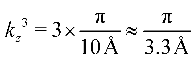 . As a result, as presented in Table 1, the densities of states become directly dependent on Lz, see the ESI,† Section S1 for the corresponding derivations.


 ) than the HOMO splitting and qualitatively this difference translates into larger HOMO bandwidths and higher hole mobility. In turn, this difference is crucial in both optical upward and downward transitions and recombination processes within the nanosheet.53

