
 Open Access Article
 This Open Access Article is licensed under a Creative Commons Attribution-Non Commercial 3.0 Unported Licence
Multivalency-induced structural variations of 2D selenium nanosheets: facile solution-phase synthesis and optical properties†
Swathi
V. M.
 a,
Arjun
K.
b,
Anju
Rajan
a,
Raghu
Chatanathodi
a,
Karthikeyan
Balasubramanian
b and
Aji A.
Anappara
*a
a,
Arjun
K.
b,
Anju
Rajan
a,
Raghu
Chatanathodi
a,
Karthikeyan
Balasubramanian
b and
Aji A.
Anappara
*a
aDepartment of Physics, National Institute of Technology Calicut (NITC), Kozhikode, Kerala 673601, India. E-mail: aji@nitc.ac.in
bNanophotonics Laboratory, Department of Physics, National Institute of Technology, Thiruchirappalli 620 015, India
First published on 22nd July 2024
Abstract
The structural stability of two-dimensional (2D) phases derived from bulk selenium (Se) is intrinsically rooted in the multivalent nature of the material. The emergence of 2D Se, as its morphology evolves from 1D to 2D, was initially inspired by theoretical predictions of various quasi-stable structural phases of 2D Se. Here, we report a facile liquid-phase synthesis of free-standing few-layer selenium nanosheets (SeNS) employing a simple magnetic stirring of their bulk counterpart in N-methyl pyrrolidone (NMP). The synthesized SeNS possess lateral dimensions ranging from several hundreds of nanometers to a few microns, with a minimum thickness of ∼1 nm. High-resolution transmission electron microscopy reveals the existence of α- and β-selenene. Fourier transform infrared analysis suggests that the inherent surface/edge functionalization of 2D SeNS by NMP enhances their dispersion stability. The UV-vis-NIR absorption spectrum of SeNS exhibits a shoulder peak at 330 nm, attributed to surface/edge functionalization, and multiple peaks across the vis-NIR region, stemming from size quantization effects. The functionalized selenium nanosheets generate photoluminescence that spans the blue-green range, while the size quantization of SeNS leads to green-orange luminescence. The non-linear optical studies following Z-scan experiments with an open aperture revealed reverse saturable absorption (RSA) and strong optical limiting in 2D SeNS under 532 nm, 10 ns laser pulses. Notably, a transition from RSA to saturable absorption (SA) has also been observed in samples stirred over an extended period. In this perspective, the results illustrate the first experimental realization of free-standing multivalent 2D selenium in allotropic forms with unique optical properties.
Introduction
The valency of an element decides its bonding behaviour with other atoms. Multivalency adds further complexity to the properties of materials by allowing the chemical species (atoms, molecules, or ions) to have different valencies and form various types of chemical bonds. Metalloids such as boron (B), silicon (Si), germanium (Ge), antimony (Sb), selenium (Se), tellurium (Te), and polonium (Po) are prime examples of this phenomenon, as they demonstrate multiple oxidation states because of their intermediate electronegativities.1,2 When downsizing these bulk materials to 2D, the abundance of atoms and dangling bonds on the surface can significantly alter the bonding patterns themselves due to the multivalent nature of the atoms. Therefore, diverse arrangements of atoms within lattice structures provide a pathway to attain various forms of the same element, each possessing distinct band structures and thus different optoelectronic properties. 2D structures, such as silicene, germanene, borophene, tellurene, and stanene, derived from non-layered (non-van der Waals) bulk elemental materials, have been reported in their allotropic form through theoretical and preliminary experimental analyses.3–10 However, analysis of the formation of various crystal structures in the 2D regime remains to be explored, which is essential for comprehending their unique properties.First principles density functional theory (DFT) calculations have predicted the formation of mono-elemental chalcogen-based systems, as illustrated by 2D tellurene and selenene, with the exploration extending to 2D polonium. In this context, multivalency plays a crucial role in determining the thermodynamic stability of lattice symmetries and layering behaviours in 2D crystal phases, giving rise to unique properties such as high carrier mobility, ferroelectric properties and excellent superconducting characteristics.11–14 Very recently, it has been shown that fabricating 2D tellurene using a top-down approach can induce structural changes that significantly affect its electronic properties.15 Theoretically, selenium is found to exhibit various 2D allotropic forms, including trigonal 1T-MoS2 like α-selenene (α-Se), tetragonal β-selenene (β-Se), and 2H-MoS2 like γ-selenene (γ-Se).11,16,17 Usually, α-Se is found to be the most stable configuration containing three Se atoms per unit cell. The structural resemblance of α-Se with the 1T-MoS2 monolayer discloses two types of Se atoms with different coordination numbers. The Se atom at the centre (Mo position) has 6 and Se atoms in the upper and lower layers (S-positions) have 3 coordination numbers with 4 nearest neighbours. In contrast, β-Se comprises chair-like six-membered and planar four-membered rings stacked alternately. Despite theoretical predictions, the experimental revelation of 2D selenium in allotropic forms remains challenging.
Qin and his co-authors reported the fabrication of 2D selenium nanosheets on Si/SiO2 substrates through physical vapour deposition (PVD) having a large lateral dimension (30 μm) with high singular crystallinity.18 In contrast to bottom-up techniques like PVD and molecular beam epitaxy (MBE), which require appropriate substrates, the goal is to utilize freestanding 2D selenium nanosheets.10 Moreover, the difficulty in achieving large-scale synthesis of 2D Se, along with complicated experimental conditions, provided a pathway for liquid-phase exfoliation of selenium due to its unique chain structure.19,20 The highly anisotropic Se, composed of one-dimensional (1D) van der Waals helical chains, exhibits different 2D structures depending on the cutting direction of bulk Se.21,22 Cutting the Se–Se covalent bond along the (001) plane normal to the c-axis can result in the formation of α-Se.23 The process of stripping off a few chains from bulk selenium to form nanosheets could be considered as cleaving along the (100) plane to obtain β-Se.24 Thus, employing gentle methods like stirring bulk materials in a suitable solvent could be a better way to obtain the inhomogeneous combination of both α-Se and β-Se, which facilitates the analysis of structural reformation in 2D materials. In this strategy, stirring may cause the entire solution to rotate, but the effect would be delayed as it reaches the top of the solution. As a result, the different layers of the solvent experience a frictional force in between, which could help to fragmentize the Se added to it.
This work reports a facile top-down synthesis strategy to obtain free-standing few-layer selenium nanosheets (SeNS) from the crystalline bulk Se powder. The simple magnetic stirring of selenium in NMP under ambient conditions (room temperature and air atmosphere) followed by centrifugation results in SeNS. As-prepared ultrathin SeNS (thickness ∼1–3 nm) show lateral dimensions in the ∼0.1–2 μm range and the HRTEM images reveal the existence of 2D allotropes of selenium, such as α- and β-selenene. The FTIR study of the samples indicates the inherent surface functionalization of 2D SeNS, which arises from the functional groups in the solvent NMP, thereby facilitating the dispersion stability of the nanosheets. The optical characterization of SeNS using a UV-vis-NIR spectrometer demonstrates significant absorption traits in the UV region (250–400 nm). Consequently, exciting the sample in this specific range induces excitation wavelength-dependent emission behaviours within the UV-vis region, explicitly spanning from 300 to 500 nm. Absorption peaks in the visible spectral range (400–600 nm) are attributed to the quantization effects of SeNS, and the corresponding luminescence effect is noted to be excitation-independent at 564 and 608 nm. In this regard, the findings enable the first experimental realization of free-standing few-layer selenium nanosheets in allotropic forms and their optical characteristics. Furthermore, we note that conducting open aperture Z-scan studies of SeNS under 532 nm, 10 ns laser pulses could yield a more favourable non-linear absorption coefficient (βNL) value. Additionally, a switch in the nonlinear optical behaviour has been observed from RSA to SA, suggesting the potential applications of SeNS in both optical limiting (OL) and Q-switching devices.
Experimental
Materials
Commercially available selenium powder (Se, 99.99%), with a standard mesh size of 100 (150) μm, and toluene (anhydrous 99.8%) were purchased from Sigma-Aldrich. N-Methyl-2-pyrrolidone (NMP, AR 99.5%, SRL chemicals) was the solvent used for the synthesis. All chemicals were used as supplied without further purification. All solvents used were of analytical reagent grade.Synthesis of selenium nanosheets
SeNS were prepared using a simple approach involving mechanical stirring of the dispersion with a magnetic stirrer. In a typical procedure, 50 mg of bulk Se powder was immersed in 10 mL of NMP solvent. The mixture was then subjected to 5 minutes of bath sonication to achieve a uniform dispersion of selenium particles in the solvent, effectively breaking down agglomerates. Subsequently, continuous stirring was maintained for three different durations, namely 1 day, 3 days, and 5 days, and the resulting samples were labelled as SeNS-1, SeNS-3 and SeNS-5. Following the stirring process, the supernatant was collected and centrifuged at 2000 rpm for 5 minutes to remove bulk selenium, leaving the supernatant enriched with selenium nanosheets. Next, the solution underwent a second centrifugation at 8000 rpm, and the resulting precipitate was collected. These collected nanosheets were rinsed twice with toluene and subsequently dried in a vacuum oven at 50 °C to facilitate further characterization.Instrumentation
Scanning electron microscopy (SEM) images and energy dispersive spectra (EDS) were recorded using a scanning electron microscope (Jeol 6390LA/OXFORD XMX N) to identify the morphology and elemental compositions of the bulk sample in powder form. The specimen for SEM analysis was obtained by spreading selenium powder on a conducting carbon tape. Besides, the crystalline properties of bulk Se, as well as SeNS-1, were determined using an X-ray diffractometer (Bruker D8 Advance: Cu Kα, λ = 1.54060 Å) to ensure structural stability. XRD analysis was carried out using the bulk selenium powder and dried SeNS-1 powder washed in toluene. The morphology and crystallinity of SeNS-1 were analyzed using transmission electron microscopy, TEM (Tecnai G2 F20 from FEI). Selected area electron diffraction (SAED) patterns and high-resolution transmission electron microscopy (HRTEM) images were also recorded to investigate the atomic arrangement of the sample. The samples for TEM measurements were prepared by drop-casting SeNS-1 dispersion onto a copper grid, and the solvent, NMP, was dried under ambient conditions. The thickness of SeNS-1 was confirmed via AFM (Bruker Multimode-8), and the studies were conducted after spin-coating the dispersion of SeNS-1 in NMP onto a glass slide, followed by drying in air. A high-resolution Raman microscope (Labram HR Evolution CCD Model: 1024 × 256-OE) was used to obtain the vibrational modes of the system at room temperature utilizing a laser of 785 nm wavelength as the light source. Raman analysis was carried out using bulk selenium and dried SeNS-1 in powder form. The surface functional groups on SeNS-1 dispersed in NMP were detected using a Fourier transform infrared (FTIR) spectrometer (PerkinElmer, Spectrum Two) in ATR mode. Optical absorption was performed using a UV-vis-NIR spectrophotometer (PerkinElmer, Model: Lambda-750) using NMP as the reference. An LS-55 fluorescence spectrophotometer (PerkinElmer) was used to measure the photoluminescence (PL) spectra of SeNS-1 dispersed in NMP under ambient conditions (room temperature and air atmosphere). A Fluorolog 3 TCSPC, Horiba, provided the corresponding lifetime data in the dispersion form.Results and discussion
Analysis of bulk selenium
The morphology of bulk Se powder was characterized using a scanning electron microscope (SEM). The SEM images in Fig. S1 (ESI†) show that the bulk Se powder has a particle size of a few hundred micrometres. At higher magnification, the structure seems to be composed of microscopic particles interconnected with one another. In Fig. S2 (ESI†), the EDS analysis of the bulk Se powder confirms the absence of other elements, which ensures the purity of the selenium powder used to synthesize SeNS-1. The crystalline properties of bulk Se are determined using an X-ray diffractometer, as shown in Fig. S3 (ESI†), and the diffraction peaks at 23.57°, 29.69°, 41.40°, 43.68°, 45.48°, 51.82°, 55.60°, 56.12°, 61.27°, 61.71°, 65.28°, and 71.67° correspond to (100), (101), (110), (102), (111), (201), (003), (112), (103), (202), (210) and (113) planes of Se according to the trigonal selenium phase (JCPDS: 06-0362).25 The crystal structure of bulk Se in Fig. S4 (ESI†) was obtained from density functional theory (DFT) calculations. The optimized lattice parameters, a = 4.46 Å and c = 5.05 Å, match well with those calculated from XRD data. In Fig. S5(a) (ESI†), the UV-DRS spectrum of bulk selenium powder shows broadband absorption in the UV-vis spectral range (200–700 nm). By employing a Tauc plot, the bandgap (Eg) of powdered selenium was found to be 1.85 eV, as seen in Fig. S5(b) (ESI†).26,27Physico-chemical properties of few-layer SeNS-1
SeNS-1 was obtained by stirring bulk Se in NMP (various solvents were selected to prepare SeNS-1 samples, and NMP was chosen to synthesize SeNS-1 due to higher concentration; for additional details, refer to the ESI,† Section V and Fig. S6) and its morphology was examined using TEM, which revealed the presence of sheet-like nanostructures. Fig. 1(a) illustrates that selenium nanosheets adhere to one another with lateral dimensions spanning several hundreds of nanometres. A few of them exhibited notably large area sheets, exhibiting lateral dimensions on the order of a few micrometres (see ESI,† Fig. S7(a)–(g)). A high-resolution TEM (HRTEM) image, as shown in Fig. 1(b), was captured to scrutinize the atomic positioning of the selenium nanosheets. Fig. 1(c) depicts the fast Fourier transform (FFT) performed on the HRTEM image displayed in Fig. 1(b), which verified that the Se nanosheets have a crystalline feature for a considerable range of area. In most cases, a selected area electron diffraction (SAED) pattern of ordered diffraction spots is observed, which signifies the crystalline nature, as shown in Fig. S8(a) (ESI†). However, in some instances, the SAED pattern of random diffraction spots is evident, indicating polycrystalline nature as depicted in Fig. S8(c) (ESI†) (see Fig. S8 (ESI†) for additional SAED images and Section VII (ESI†) for detailed SAED pattern indexing). Fig. 1(d) corresponds to the enlarged portion of Fig. 1(b), presenting an atomically resolved HRTEM image of the nanosheets recognizing the locations of selenium atoms, with the unit cell containing three atoms. The distance between two lattice fringes is 0.22 nm, indicating the (110) plane of Se. Fig. S7h and i (ESI†) demonstrate the additional HR-TEM images showing different d-spacings; insets (1) and (2) imply d-spacings of 0.15 nm and 0.13 nm corresponding to (202) and (113) lattice planes.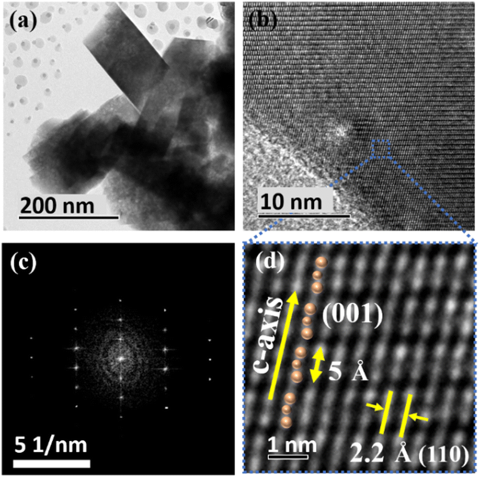 | ||
| Fig. 1 (a) and (b) TEM images of as-prepared large area SeNS-1 and (c) the corresponding high-resolution TEM image. The inset shows the FFT of the same. (d) Magnified HRTEM image indicating the typical selenium chains along the c-axis. | ||
The atomic arrangements within the nanosheets were analyzed by capturing HRTEM images of different regions of various nanosheets in Fig. 2(a)–(f). Fig. 2(a) and (b) present atomically resolved HRTEM images of SeNS-1, enabling the identification of selenium atom positions. The atomic arrangement depicted in Fig. 2(b), employing a ball-and-stick model, is overlaid on HRTEM to emphasize the rectangular unit cell of β-selenene, featuring in-plane lattice constants a ≈ 4.1 Å and b ≈ 4.9 Å. In addition, the expanded views of Fig. 2(c) and (e) are shown in Fig. 2(d) and (f), respectively. In Fig. 2(d), the HRTEM image shows the top view of the arrangement of selenium atoms in α-Se with a unit cell of 3.7 × 3.7 Å. In Fig. 2(f), the side view of α-Se is illustrated, revealing a buckling height (d) between two adjacent selenium layers of ≈3.1 Å.
 | ||
| Fig. 2 (a) HRTEM image of drop-cast SeNS-1 and (b) the schematic representation of the top view of β-selenene. (c)–(f) the HRTEM images of α-selenene. The top and side views of α-selenene are shown in (d) and (f) respectively. | ||
The crystal structure and in-plane lattice constants obtained are in accordance with the predicted α and β-Se phases.14,28 The structural parameters were calculated using density functional theory (DFT) as implemented in the Vienna Ab initio Simulation Package (VASP) to confirm the crystal structure and the lattice constants.29,30 The relaxed crystal structures of α- and β-selenene monolayers determined from DFT calculations are shown in Fig. S9 (ESI†). The details of the DFT computations can be found in the ESI† (Section VIII), which are in good agreement with experimental data obtained from HRTEM.
Atomic force microscopy (AFM) was employed to assess both the thickness and topographical morphology of SeNS-1. As illustrated in the insets of Fig. 3(a) and (b), the thickness falls within the range of ∼1 nm to ∼3.6 nm, while the lateral dimensions are extended to a few micrometres. The height measurements shown in Fig. 3(a) correspond to bilayer SeNS-1, assuming that the monolayer selenium is 0.5 nm thick, and Fig. 3(b) displays SeNS-1, with dimensions of 1.4 nm and 3.6 nm, respectively.18 The visible dark spots on the surface can be attributed to defects that are likely formed during the synthesis process. As a result, roughness could be observed on the surface of the nanosheets in Fig. 3(a). Fig. 4(a) demonstrates the XRD pattern of SeNS-1 following the trigonal selenium. The peak at 2θ = 29.69° has the most significant intensity representing the lattice plane of (101), and the intensity of the remaining peaks has lowered concerning the peaks of bulk Se. Furthermore, the broadening of peaks corresponding to the planes (101), (110), (111) and (102) is notable compared to bulk selenium, which is in good agreement with the formation of 2D SeNS-1 (XRD data of SeNS-3 and SeNS-5 are given in Fig. S10(a), ESI†).
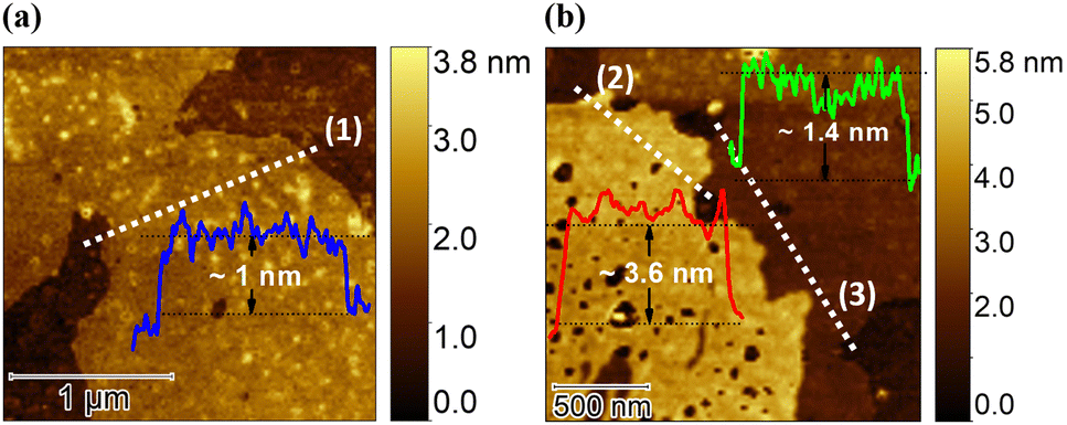 | ||
| Fig. 3 (a) and (b) AFM images of few-layer SeNS-1 presenting lateral thickness (white broken line) and the corresponding height profiles (insets). | ||
 | ||
| Fig. 4 (a) XRD data of SeNS-1 and bulk selenium. (b) Raman spectra of bulk selenium and SeNS-1 (c) Schematic representation of the Raman modes in trigonal Se along with the atomic motion. (d) FTIR spectra of NMP and powder form of SeNS-1 in ATR mode. | ||
We analysed the structural discrepancy of SeNS-1 with respect to bulk Se using Raman spectroscopy, and the presence of three Raman-active vibrational modes was observed in Fig. 4(b) for bulk Se. The out-of-plane vibrations and in-plane vibrations of Se atoms along the c-axis in Fig. 4(c) correspond to a combination of A1 and E2 modes of vibrations at approximately 235.5 cm−1 and 238.7 cm−1.
This observation is consistent with the characteristics of the trigonal selenium (t-Se) phase. The low-intense broad peak at 144.4 cm−1 (E1) was ascribed to the rotation mode of the a-axis. Meanwhile, it is worth noting that the identified peaks for two distinct spots of the SeNS-1 sample, say SeNS-1 (Spot-1) and SeNS-1 (Spot-2) in Fig. 4(b), exhibited a red shift of 1.6 cm−1 for both A1 and E2 modes of vibration when compared to the peak positions of bulk selenium.23 The Raman spectra of SeNS-3 and SeNS-5 exhibited a larger red shift (2.2 cm−1) in the A1 and E2 modes of vibration, as shown in Fig. S10(b) (ESI†). However, a 0.8 cm−1 red shift occurred in the E1 mode, indicating that the rotation mode is less responsive than the stretching modes of vibration while reducing the thickness of bulk selenium. Notably, this redshift is consistent across all SeNS samples, suggesting that the duration of stirring does not affect the rotation mode of the a-axis. The experimental Raman spectra of SeNS-1, SeNS-3, and SeNS-5 closely resemble that of the bulk t-Se phase, with the noted peak shifts. A previous Raman study on ultrathin selenium flakes oriented along the (001) plane confirms the presence of the α-Se phase for the prepared SeNS-1, SeNS-3, and SeNS-5 samples.23 The apparent red shift of A1 and E2 modes of SeNS-1 might stipulate the presence of stress in the modifications of the synthesized SeNS-1.31 Moreover, the peak intensity of E2 and A1 modes exhibits significant changes for SeNS-1 (Spot-1) and SeNS-1 (Spot-2), which can be due to distinct c-axis orientations with the direction of polarisation of light used in Raman analysis.18
To get a clear idea of the functional groups present in SeNS-1, infrared absorption was analyzed using an FTIR spectrometer. The infrared (IR) spectra of both the solvent NMP and SeNS-1, featuring several distinct peaks within the wavenumber range of 500–4000 cm−1, are illustrated in Fig. 4(d). The weak and broad feature around 3500 cm−1 indicates the absorption of moisture by NMP.32 The absorption patterns of SeNS-1 resemble that of NMP with reduced intensity. The characteristic peaks at 2939 and 2881 cm−1 represent the C–H bond stretching vibrational mode compared with the bonds of NMP. A strong carbonyl (–C![[double bond, length as m-dash]](https://www.rsc.org/images/entities/char_e001.gif) O) stretch region at 1649 cm−1 is also visible in the spectrum of SeNS-1, with an ∼30 cm−1 shift to a lower wavenumber. Indeed, the surface states of SeNS-1, coupled with carbonyl functional groups, render it emissive, according to the prior report on carbon dots.33 From the FTIR study, we can deduce that SeNS-1 is surface-functionalized with functional groups originating from NMP, which contributes to its dispersion stability in the solvent. Furthermore, the luminescence observed may be attributed to the hybridization of oxidized carbon groups, such as carbonyl groups, with the surface of SeNS-1.
O) stretch region at 1649 cm−1 is also visible in the spectrum of SeNS-1, with an ∼30 cm−1 shift to a lower wavenumber. Indeed, the surface states of SeNS-1, coupled with carbonyl functional groups, render it emissive, according to the prior report on carbon dots.33 From the FTIR study, we can deduce that SeNS-1 is surface-functionalized with functional groups originating from NMP, which contributes to its dispersion stability in the solvent. Furthermore, the luminescence observed may be attributed to the hybridization of oxidized carbon groups, such as carbonyl groups, with the surface of SeNS-1.
Linear optical properties of few-layer SeNS-1
To scrutinize the optical properties of the SeNS-1 dispersion, we performed UV-vis-NIR studies and photoluminescence measurements at room temperature. The solvent NMP was used as the reference sample for the absorption measurement. In the UV range (from 250 to 400 nm), the absorption data (Fig. 5(a)) exhibit a sharp peak at 277 nm (4.47 eV) followed by a broad shoulder peak at 330 nm (3.75 eV). The significant peak at 277 nm may have originated from the interband and core electronic transitions of SeNS-1.34 Furthermore, surface functional groups triggered by the solvent NMP could be the probable source of the extensive absorption at 330 nm. Thus, to monitor the emission traits of the SeNS-1 dispersion due to the absorption in the UV region, the excitation wavelength was altered from 240 to 400 nm with an incremental step of 20 nm. Fig. 6(a) shows multi-wavelength photoluminescence (PL) emission with excitation-dependent properties covering the range of 300–600 nm. As depicted in Fig. 6(b), the emission peaks move towards longer wavelengths when the excitation wavelength undergoes a red shift. The PL intensity increases with the increase in the excitation wavelength, reaches the maximum emission around 400 nm at λex = 300 nm, and becomes less significant for excitation wavelengths longer than 400 nm, as shown in Fig. 6(c). | ||
| Fig. 5 (a) UV-vis-NIR absorption spectrum of the SeNS-1 dispersion with NMP as the reference. Band structures of monolayers of (b) α-Se and (c) β-Se determined using the HSE06 exchange–correlation functional. | ||
 | ||
| Fig. 6 (a) Photoluminescence spectra of the SeNS-1 dispersion at the excitation wavelengths ranging from 240 nm to 420 nm with the step-size of 20 nm. (b) Shifting of the emission peak with respect to the excitation wavelengths. (c) Change in PL intensity according to the excitation wavelength. | ||
To identify multiple emission centres, Gaussian fittings of the emission spectra were performed at various excitation wavelengths (280 nm, 295 nm, 330 nm, and 380 nm), as depicted in Fig. S11 (ESI†). It was observed that these spectra were composed of five emission peaks arising from distinct emission states. Different peaks exhibit dominant characteristics under varying excitation conditions, leading to excitation-dependent behaviour. The collected excitation spectra, corresponding to emission wavelengths ranging from 340 nm to 480 nm in 20 nm increments, are presented in Fig. S12 (ESI†), highlighting the presence of multiple excitation centres, as indicated by the grey dotted lines. However, the peak at 252 nm did not shift with the emission wavelengths, as depicted by the red dotted line, which may result in the emission peak at 300 nm with less intensity.
The excitation wavelength-independent nature of this emission was clearly visible in Fig. S13 (ESI†). The relative quantum yield (QY) of the SeNS-1 dispersion was calculated using quinine sulphate as a reference and was determined to be 10.88% (QY calculations are given in Section XIII (ESI†)).
In the absorption spectrum of the SeNS-1 dispersion collected at vis-NIR wavelengths (400–1300 nm), three peaks were observed at 485 nm, 523 nm and 563 nm, with a shoulder peak at 598 nm.
The spectrum was featureless from 700 nm to 1100 nm, and a broad peak was observed at 1169 nm and another shoulder at 1280 nm. Theoretical investigations of various 2D selenium allotropes, such as α-Se and β-Se, have demonstrated the possibility of thickness-dependent bandgaps that are influenced by their multivalent nature, crystal structure and quantum confinement effect. The absorption spectrum containing peaks at 485 nm (2.55 eV), 563 nm (2.2 eV), and 598 nm (2.07 eV) indicates the presence of layer-dependent bandgaps of β-Se in the SeNS-1 dispersion (c, e and f from the left inset of Fig. 5(a)).35 Prior research on few-layered phosphorene and tellurene has shown similar spectral characteristics.15,36 The absorption behaviour around 523 nm (2.37 eV) corresponds to the interband transition of α-Se (d from the left inset of Fig. 5(a)).37 Moreover, a notable absorption peak was observed in the near-infrared region around 1169 nm, which can be associated with the monolayer of α-Se.14,38 The electronic band structure of 2D Se was calculated using DFT to analyze the absorption spectrum. Fig. 5(b and c) show theoretically obtained bandgaps of 1.11 eV for a monolayer of α-Se and 2.59 eV for a monolayer of β-Se, consistent with the optical absorption obtained from the SeNS-1 dispersion. The bandgaps of the bilayer and trilayer of β-Se are given in Fig. S16(b) and S17(b) (ESI†). The theoretical bandgap values are obtained using the HSE06 hybrid functional. We have also calculated the bandgap and optical absorption edge using PBE exchange–correlation, which agree well with each other (refer to Fig. S14–S17 in Section XIV of ESI†); however, it is noted that these values do not match well with the HSE06 band gap or the experimentally obtained values. This discrepancy is well known since HSE06 contains the exact exchange from Hartree–Fock theory. Thus, the absorption peaks of α and β-Se in Fig. 5(a) ensure the stability of 2D allotropic forms in the synthesized sample.
Unexpectedly, during our investigation of the PL behaviour, while exciting the dispersion of SeNS-1 in the visible region (400–600 nm), we observed predominant emission peaks at 564 and 608 nm, as illustrated in Fig. 7(a). The excitation wavelength was increased in steps of 20 nm. SeNS-1 displayed excitation-independent emission with 564 and 608 nm peaks, consistent with band gap behaviour. When the sample was excited at 510 nm, the emission with maximum intensity was observed at 564 nm. The spectra showed a maximum for the emission intensity at 608 nm when excited at 550 nm. Although the excitation spectra shown in Fig. 7(b) correspond to λem = 564 nm and 608 nm, they closely align with the absorption peaks that arise from the size-quantization of 2D SeNS-1. Hence, it is evident that the origin of the emission in the visible region at 564 nm and 608 nm was concluded to be from the size-quantization effect of the SeNS-1 obtained.
 | ||
| Fig. 7 (a) Photoluminescence spectra of dispersion of SeNS-1 in NMP at excitation wavelengths ranging from 400 to 600 nm in 20 nm increments. (b) Excitation spectra collected at emission wavelengths 564 nm and 608 nm. (c) Contour plot of the SeNS-1 dispersion in NMP covering the excitation wavelength from 200 to 600 nm. | ||
Moreover, Fig. 7(c) depicts the 3-D PL intensity plotted as a function of emission and excitation wavelengths. This contour plot acquired from the excitation–emission matrix confirms that the emission depends on the excitation wavelengths represented by a white dotted line. The horizontal red dotted lines denoted excitation-independent emission in the visible range due to the size-quantization effect of SeNS-1. So, the absorption and the emission traits could remarkably confirm the surface functionalization and the size-quantization of SeNS-1 achieved via a simple solution synthesis technique. However, the contour plot derived from the excitation–emission matrix (EEM) of bulk selenium powder did not exhibit any notable emission characteristics. Furthermore, to confirm the presence of multiple emission bands, we performed lifetime measurements of the SeNS-1 dispersion. It exhibits a triple exponential decay at excitation wavelengths 295 nm and 330 nm, pointing to various emissive sites of the PL process. The PL lifetime was fitted using a triple exponential fitting function, and the fitting parameters are presented in Table IV (ESI†). The average lifetime obtained for SeNS-1 at λem = 430 nm is about 33.3 ns (see ESI†, Fig. S19). The lifetime drops to 28 ns at the emission wavelength of 400 nm. This may be due to the diminished rate of carrier recombination of electrons and holes in SeNS-1, where contributions from multiple emission centres vary according to the change in its excitation wavelength from 295 nm to 330 nm.39 However, the lifetime was measured in the visible region using 570 nm as the excitation wavelength and a double exponential decay was observed with an average lifetime of 41 ps.
Fig. S20 (ESI†) shows the proposed graphical representation of the transitions in the energy levels of SeNS-1. Absorption within the selenium's core electronic level yields UV emission around 300 nm, albeit with less emission intensity. The UV-vis absorption of SeNS-1 occurs at different energy states that arise due to the hybridization of the functional groups with the dangling bonds of SeNS-1. Thus, the emission occurs from multiple energy surface states, leading to the excitation wavelength-dependent PL in the 300–500 nm range. Also, the radiative decay from the quantized states shows excitation-independent emission behaviour in the visible spectral range. The energy levels in the SeNS-1 dispersion in NMP show significant absorption at both 532 nm and 266 nm. These wavelengths are important for single-photon absorption and represent twice the photon energy due to size quantization and direct band transition of selenium, as depicted in Fig. 8. Consequently, investigating the nonlinear optical (NLO) properties using a 532 nm laser becomes intriguing to understand the response of SeNS to intense light pulses, potentially paving the way for designing photonic devices such as limiters or mode-locking applications.
 | ||
| Fig. 8 Schematic representation illustrating the energy levels and electronic transitions (SPA and 2PA) in SeNS-1. | ||
Non-linear optical properties
To investigate the NLO responses of the synthesized SeNS and to compare their NLO parameters, we employed the Z-scan technique with 532 nm pulsed laser irradiation at room temperature. This method evaluates the nonlinearity of the samples by analyzing the transmission of a Gaussian beam through the sample relative to the input intensity or fluence. To perform this analysis, we utilized a Q-switched Nd-YAG laser as the excitation source. It emits a 10 ns pulse at a second harmonic wavelength of 532 nm with a repetition rate of 10 Hz, producing linearly polarized light. A custom-designed beam splitter, allowing for 70% transmission and 30% reflection of incoming beams, was employed to receive the excitation source. Pyroelectric energy sensors, linked to a dual-channel power meter, simultaneously recorded the energies of both transmitted and reflected laser beams. The transmitted laser beam underwent focusing via a convex lens with a focal length of 25 cm. To maintain consistent linear transmission, it was kept at 70% for all samples. The sample was positioned on an automated translational stage, facilitating precise shifting of the samples along the direction of the focused laser beam.A pulse energy of 40 μJ was utilized to evaluate the optical nonlinearities of the samples. When the samples are positioned at the focal point, the intense laser beam causes a deviation from Beer's law, manifesting as nonlinearity. This nonlinearity often results in a variation in transmittance relative to the incident fluence, leading to either a decrease (reverse saturation absorption) or an increase (saturation absorption). Numerous nonlinear mechanisms, including two-photon absorption (2PA), three-photon absorption (3PA), multiphoton absorption, free carrier absorption (FCA), nonlinear scattering (NLS), and excited state absorption (ESA), among others, collectively contribute to this nonlinear absorption phenomenon.
To accurately determine the degree and features of this nonlinearity, a variety of nonlinear transmission equations involving 2PA and 3PA were utilized to describe the experimental data. Eventually, combining 2PA with the saturation transmission equation led to the best theoretical fit. The following formula can be used to get the sample's normalized transmittance,40
 | (1) |
 , where I0 indicates the focus point's maximum intensity (Z = 0) and Z indicates the Rayleigh range, which is computed as πω02/λ. In this case, the excitation wavelength is denoted by λ, while the focal point beam radius is indicated by ω0. The effective length (Leff) is represented as
  , where l is the sample's route length. The normalized optical transmittance of SeNS-1, SeNS-3, and SeNS-5 dispersions in NMP is shown in Fig. 9(a)–(c). Solid spheres denote the original experimental Z-scan data, while a solid line depicts the theoretical fit based on the previously mentioned equation. The transmittance of SeNS-3 at Z = 0 decreases, indicating a pronounced RSA effect in Fig. 9(a). Extending the stirring time to 3 and 5 days (Fig. 9(b) and (c)) transforms the nonlinear optical behaviour of the selenium nanosheet dispersion from RSA to SA. As depicted in Fig. 9(d), the absorption peaks of SeNS-3 and SeNS-5 are shifted to longer wavelengths (∼300 nm) compared to SeNS-1 (see the normalized absorption spectra in Fig. S21(b), ESI†), suggesting that absorption comes from new energy levels. The deconvoluted peaks of the absorption spectra are given in Fig. S21(c) and (d) (ESI†). The peaks observed around 271 nm and 274 nm in Fig. S16(c) and (d) (ESI†) arise from transitions from the bands corresponding to 3s2p6d10 to the conduction band of selenium.34 It is noteworthy that the contribution of this absorption gradually diminishes with increasing stirring time. New peaks detected at 290 nm and 302 nm for the SeNS-3 sample might be associated with additional surface functionalization due to excessive stirring, primarily owing to the presence of carbonyl groups (–CO).41 The RSA observed solely in SeNS-1 originates from 2PA, demonstrating its optical limiting effect.42–45
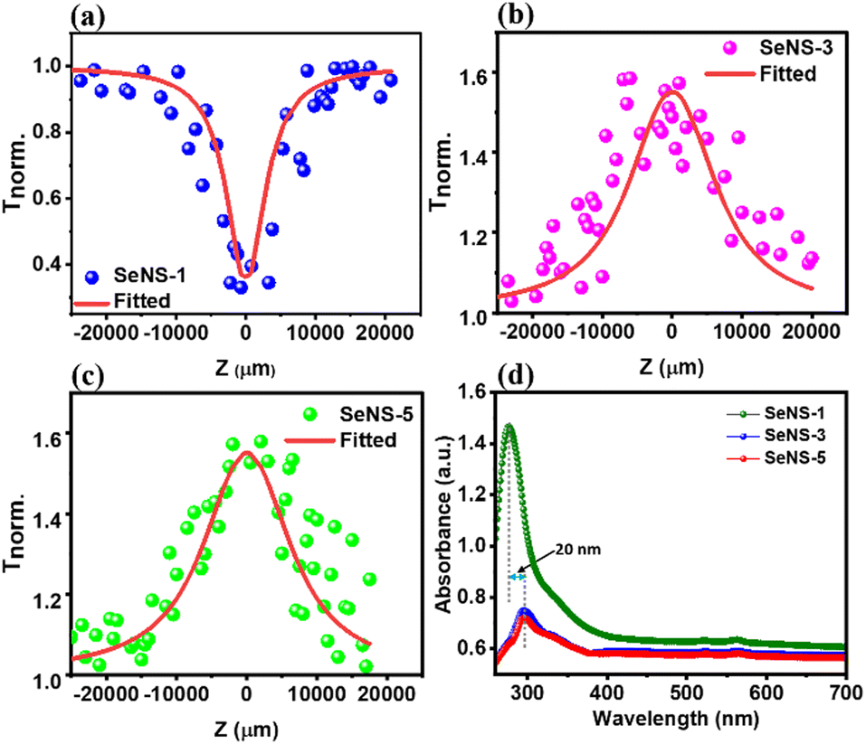 | ||
| Fig. 9 The open aperture Z-scan experimental results of SeNS for samples (a) SeNS-1, (b) SeNS-3, and (c) SeNS-5. (d) UV-vis absorption spectra of the same. | ||
At lower intensity, i.e., away from the focus, single photon absorption (SPA) takes place. By moving the sample position closer to the focus of the beam, 2PA could occur, as absorption around 266 nm is prominent for the sample SeNS-1. Hence, a large decrement in the normalized transmission at Z = 0 is observed, resulting in RSA. The transformation from RSA to SA with increasing stirring time may be attributed to the bleaching of electrons from the valence band. The effective peak shift towards 300 nm, resulting from the emergence of new energy levels, weakens the probability of 2PA. Consequently, single photon absorption can be enhanced at higher intensity, further obstructing the absorption of photons and resulting in increased optical transmittance, thereby leading to SA.
NLO parameters such as saturation absorption intensity (Is) and the non-linear absorption coefficient (βNL) are tabulated in Table V (ESI†). The magnitude of βNL for SeNS-1 is found to be 30 cm GW−1, which is a 200% increment with respect to the previous reports.42 The nonlinear absorption coefficient undergoes a notable decrease with increasing stirring time, measuring 0.005 cm GW−1 for SeNS-3 and 0.001 cm GW−1 for SeNS-5. The prepared samples thus demonstrate the significant potential of SeNS as a promising candidate for NLO applications, serving as a fundamental material in optical limiting and Q-switching devices.
Conclusions
In summary, SeNS-1 in the solvent NMP was successfully fabricated by a facile, low-cost magnetic stirring method. As-synthesized SeNS-1 (thickness ∼1–3 nm) shows lateral dimensions in the range of ∼0.5–2 μm and the HRTEM images reveal the existence of 2D allotropes of selenium, such as α- and β-selenene. The FTIR study of the sample revealed that SeNS-1 is surface-functionalized with groups from NMP, which facilitates its dispersion stability in the solvent. The dispersion of SeNS-1 was found to be stable for several weeks. SeNS-1 was characterized by its UV-visible absorption and subsequent light emission properties. An interesting finding of the study was the observance of the possible signatures of quantization of both α- and β-selenene from the absorption spectrum. Along with this, an entirely different emission behaviour could be identified in the boundary of the UV-visible (300–600 nm) region and visible region (564 nm and 608 nm) due to the surface-functionalization and the size-quantization effect of SeNS-1. Additionally, the transition from RSA to SA with increased stirring time suggests the modulation of optical non-linearity, possibly due to the emergence of new peaks at higher wavelengths in UV-vis absorption spectra.Data availability
The supporting data for this article are included in the ESI.†Conflicts of interest
The authors have no conflicts to disclose.Acknowledgements
The financial support from University Grants Commission (UGC), New Delhi, India is gratefully acknowledged. We thank Dr Lakshmi C (Department of Chemistry, NITC), Analytical Instrumentation Facility (SAIF) at MG University, Kottayam, Amrita Centre for Nanoscience and Molecular Medicine, Kochi, and Central Sophisticated Instrumentation Facility (CSIF), University of Calicut for providing experimental facilities and Centre for Computational Modeling and Simulation (CCMS) at NIT Calicut for providing computational facilities.References
- Y. N. Vodyanitskii, Eurasian Soil Sci., 2013, 46, 1139–1149 CrossRef.
- T. H. Keenan, Patty's Toxicology, John Wiley & Sons, Ltd, 2023, pp. 1–49 Search PubMed.
- S. Cahangirov, H. Sahin, G. Le Lay and A. Rubio, Introduction to the Physics of Silicene and other 2D Materials, Springer International Publishing, Cham, 2017, pp. 13–39 Search PubMed.
- B. Aufray, A. Kara, Ś. Vizzini, H. Oughaddou, C. Ĺandri, B. Ealet and G. Le Lay, Appl. Phys. Lett., 2010, 96, 1–4 CrossRef.
- M. E. Dávila, L. Xian, S. Cahangirov, A. Rubio and G. Le Lay, New J. Phys., 2014, 16, 95002 CrossRef.
- S. Balendhran, S. Walia, H. Nili, S. Sriram and M. Bhaskaran, Small, 2015, 11, 640–652 CrossRef PubMed.
- X.-F. Zhou, X. Dong, A. R. Oganov, Q. Zhu, Y. Tian and H.-T. Wang, Phys. Rev. Lett., 2014, 112, 85502 CrossRef.
- B. Feng, J. Zhang, Q. Zhong, W. Li, S. Li, H. Li, P. Cheng, S. Meng, L. Chen and K. Wu, Nat. Chem., 2016, 8, 563–568 CrossRef CAS PubMed.
- F. F. Zhu, W. J. Chen, Y. Xu, C. L. Gao, D. D. Guan, C. H. Liu, D. Qian, S. C. Zhang and J. F. Jia, Nat. Mater., 2015, 14, 1020–1025 CrossRef CAS PubMed.
- J. Chen, Y. Dai, Y. Ma, X. Dai, W. Ho and M. Xie, Nanoscale, 2017, 9, 15945–15948 RSC.
- Z. Zhu, X. Cai, S. Yi, J. Chen, Y. Dai, C. Niu, Z. Guo, M. Xie, F. Liu, J. H. Cho, Y. Jia and Z. Zhang, Phys. Rev. Lett., 2017, 119, 1–5 Search PubMed.
- H. Bao, B. Zhao, J. Zhang, Y. Xue, H. Huan, G. Gao and Z. Yang, Sci. Rep., 2022, 12, 2129 CrossRef CAS PubMed.
- C. Zhao, X. Cai, L. Liu, C. Liu, Z. Zeng, C. Niu, C. Xia and Y. Jia, Adv. Theory Simulat., 2021, 4, 1–9 Search PubMed.
- D. Wang, L. M. Tang, X. X. Jiang, J. Y. Tan, M. D. He, X. J. Wang and K. Q. Chen, Adv. Electron. Mater., 2019, 5, 1–6 Search PubMed.
- A. Bhui, S. Roychowdhury, A. Sen, U. V. Waghmare and K. Biswas, Z. Anorg. Allg. Chem., 2022, 648, e202200097 CrossRef.
- J. Qiao, Y. Pan, F. Yang, C. Wang, Y. Chai and W. Ji, Sci. Bull., 2018, 63, 159–168 CrossRef.
- L. Ramírez-Montes, W. López-Pérez, R. González-Hernández and C. Pinilla, Int. J. Quantum Chem., 2020, 120, 1–10 CrossRef.
- J. Qin, G. Qiu, J. Jian, H. Zhou, L. Yang, A. Charnas, D. Y. Zemlyanov, C. Y. Xu, X. Xu, W. Wu, H. Wang and P. D. Ye, ACS Nano, 2017, 11, 10222–10229 CrossRef CAS.
- Y. Tanaka, S. P. Collins, S. W. Lovesey, M. Matsumami, T. Moriwaki and S. Shin, J. Phys.: Condens. Matter, 2010, 22, 122201 CrossRef CAS PubMed.
- C. Xing, Z. Xie, Z. Liang, W. Liang, T. Fan, J. S. Ponraj, S. C. Dhanabalan, D. Fan and H. Zhang, Adv. Opt. Mater., 2017, 5, 1–10 Search PubMed.
- W.-G. Lee, Y. K. Chung, J. Lee, B. J. Kim, S. Chae, B. J. Jeong, J.-Y. Choi and J. Huh, ACS Omega, 2020, 5, 10800–10807 CrossRef CAS.
- P. Bammes, R. Klucker, E. E. Koch and T. Tuomi, Phys. Status Solidi, 1972, 49, 561–570 CrossRef CAS.
- P. V. Sarma, R. Nadarajan, R. Kumar, R. M. Patinharayil, N. Biju, S. Narayanan, G. Gao, C. S. Tiwary, M. Thalakulam, R. N. Kini, A. K. Singh, P. M. Ajayan and M. M. Shaijumon, 2D Mater., 2022, 9, 045004 CrossRef CAS.
- Z. Xie, C. Xing, W. Huang, T. Fan, Z. Li, J. Zhao, Y. Xiang, Z. Guo, J. Li, Z. Yang, B. Dong, J. Qu, D. Fan and H. Zhang, Adv. Funct. Mater., 2018, 28, 1705833 CrossRef.
- A. H. Shar, M. N. Lakhan, J. Wang, M. Ahmed, K. T. Alali, R. Ahmed, I. Ali and A. Q. Dayo, Dig. J. Nanomater. Biostruct., 2019, 14, 867–872 Search PubMed.
- S. Tutihasi and I. Chen, Phys. Rev., 1967, 158, 623–630 CrossRef.
- A. Mukherjee, D. Vasileska and A. H. Goldan, J. Appl. Phys., 2018, 124, 235102 CrossRef.
- G. Liu, Z. Gao, G.-L. Li and H. Wang, J. Appl. Phys., 2020, 127, 65103 CrossRef CAS.
- G. Kresse and J. Hafner, Phys. Rev. B: Condens. Matter Mater. Phys., 1993, 47, 558–561 CrossRef CAS PubMed.
- G. Kresse and J. Furthmüller, Phys. Rev. B: Condens. Matter Mater. Phys., 1996, 54, 11169–11186 CrossRef CAS PubMed.
- G. Lucovsky, Phys. Status Solidi, 1972, 49, 633–641 CrossRef CAS.
- H. C. Yau, M. K. Bayazıt, J. H. G. Steinke and M. S. P. Shaffer, Chem. Commun., 2015, 51(93), 16621–16624 RSC.
- Z. Sun, X. Li, Y. Wu, C. Wei and H. Zeng, New J. Chem., 2018, 42, 4603–4611 RSC.
- S. C. Singh, S. K. Mishra, R. K. Srivastava and R. Gopal, J. Phys. Chem. C, 2010, 114, 17374–17384 CrossRef CAS.
- M. Cheng, Z. Z. Zhu and G. Y. Guo, Phys. Rev. B, 2021, 103, 1–15 Search PubMed.
- P. Yasaei, B. Kumar, T. Foroozan, C. Wang, M. Asadi, D. Tuschel, J. E. Indacochea, R. F. Klie and A. Salehi-Khojin, Adv. Mater., 2015, 27, 1887–1892 CrossRef CAS PubMed.
- J. Singh, P. Jamdagni, M. Jakhar and A. Kumar, Phys. Chem. Chem. Phys., 2020, 22, 5749–5755 RSC.
- C. Liu, T. Hu, Y. Wu, H. Gao, Y. Yang and W. Ren, J. Phys.: Condens. Matter, 2019, 31, 235702 CrossRef CAS PubMed.
- F. Xue, N. Bi, J. Liang and H. Han, J. Nanomater., 2012, 2012, 751519 CrossRef.
- S. K. R. L. Sutherland and D. G. Mclean, Handbook of Nonlinear Optics, Marcel Dekker, 2003 Search PubMed.
- N. S. Alghunaim, J. Mater. Res. Technol., 2020, 9, 3502–3510 CrossRef.
- Z. Zhao, B. Du, Y. Xin, Z. Ren, F. Xing and F. Zhang, Nanotechnology, 2023, 34, 385705 CrossRef.
- A. Suslov, S. Bikorimana, P. Lama, V. Sukharenko, A. Walser and R. Dorsinville, J. Nonlinear Opt. Phys. Mater., 2017, 26, 1–9 CrossRef.
- K. A. Ann Mary, N. V. Unnikrishnan and R. Philip, Chem. Phys. Lett., 2013, 588, 136–140 CrossRef.
- F. Zhang, G. Liu, Z. Wang, T. Tang, X. Wang, C. Wang, S. Fu, F. Xing, K. Han and X. Xu, Nanoscale, 2019, 11, 17058–17064 RSC.
Footnote |
| † Electronic supplementary information (ESI) available: The details of the crystal structure, FESEM, XRD, and the UV-visible absorption spectrum (in DRS mode) of pristine Se, more TEM images, SAED patterns and their indexing, computational methodology, photoluminescence spectra, photoluminescence quantum yield calculations, electronic band structure of β-selenene, energy level diagram and lifetime calculations. See DOI: https://doi.org/10.1039/d4cp01623h |
| This journal is © the Owner Societies 2024 |