
 Open Access Article
 This Open Access Article is licensed under a Creative Commons Attribution-Non Commercial 3.0 Unported Licence
Physical and chemical properties and degradation of MAPbBr3 films on transparent substrates†
Valentina
Carpenella‡
 a,
Fabrizio
Messina‡
b,
Jessica
Barichello
c,
Fabio
Matteocci
c,
Paolo
Postorino
d,
Caterina
Petrillo
e,
Alessandro
Nucara
df,
Danilo
Dini
b and
Claudia
Fasolato
*g
a,
Fabrizio
Messina‡
b,
Jessica
Barichello
c,
Fabio
Matteocci
c,
Paolo
Postorino
d,
Caterina
Petrillo
e,
Alessandro
Nucara
df,
Danilo
Dini
b and
Claudia
Fasolato
*g
aDepartment of Science, University of Roma Tre, Via della Vasca Navale 84, 00146 Rome, Italy
bDepartment of Chemistry, Sapienza University of Rome, P.le A. Moro 5, 00185 Rome, Italy
cCHOSE, Department of Electronic Engineering, University of Rome Tor Vergata, Rome 00133, Italy
dDepartment of Physics, Sapienza University of Rome, Piazzale Aldo Moro 5, 00185 Rome, Italy
eDepartment of Physics and Geology, University of Perugia, Via A. Pascoli, 06123 Perugia, Italy
fCNR-SPIN, c/o Sapienza University of Rome, Piazzale Aldo Moro 5, 00185 Rome, Italy
gCNR-ISC, Institute for Complex Systems, c/o Sapienza University of Rome, P.le A. Moro 5, 00185 Rome, Italy. E-mail: claudia.fasolato@cnr.it
First published on 21st June 2024
Abstract
To date, the potential exploitation of hybrid organic–inorganic perovskites (HOIPs) in photovoltaic technologies has been significantly hampered by their poor environmental stability. HOIP degradation can be triggered by conventional operational environments, with excessive heating and exposure to oxygen and moisture significantly reducing the performances of HOIP-based solar cells. An imperative need emerges for a thorough investigation on the impact of these factors on the HOIP stability. In this work, the degradation of methylammonium lead bromide (CH3NH3PbBr3) thin films, deposited via spin-coating on indium tin oxide (ITO) and strontium titanate (STO) substrates, was investigated by combining Raman and ultraviolet-visible (UV-Vis) absorption spectroscopy, as well as optical and fluorescence microscopy. We assessed the physical and chemical degradation of the films occurring under diverse preservation conditions, shedding light on the byproducts emerging from different degradation pathways and on the optimal HOIP preservation conditions.
1 Introduction
Hybrid organic–inorganic perovskites (HOIPs) of chemical formula ABX3, where A is an organic cation (methylammonium MA+ = CH3NH3+, or formamidinium FA+ = HC(NH2)2+), B is a metal (Pb2+, Sn2+), and X is a halogen anion (i.e. I−, Br− or Cl−), have been considered emerging energy conversion materials, to be integrated in high performance photovoltaic technologies. Their direct bandgap is indeed conveniently found in the visible range and can be finely tuned by varying the system composition.1–5 Furthermore, they are characterized by high absorption coefficients6 and relative ease of fabrication, with low-cost materials and processes. Such favorable properties made HOIPs operational in tandem solar cells devices with power conversion efficiency (PCE) exceeding 30% in just two decades of development.7,8 However, the degradation induced by the conventional working environment of a typical solar cell, i.e. exposure to oxygen and moisture or prolonged UV irradiation, cannot be overlooked, as they could significantly decrease the performances of the device.9–11 The chemical degradation routes of HOIPs usually involve other molecular species, like H2O, that can infiltrate in the perovskite crystal lattice and occupy the space between organic cation and halogen,12 and O2. The latter, in presence of external stimuli, such as electromagnetic radiation or, to a lesser extent, temperature, can result in perovskite decomposition.13 The deterioration triggered by H2O and O2 is not exclusive, as the degradation of thin HOIP films was also observed in vacuum, i.e. a condition in which HOIP represents a closed system, without the influence of these (or other) environmental catalytic agents.14–16 Even though many hypotheses have been formulated around the degradation pathways and the chemical products of such reactions, a rationalization of the deterioration mechanisms of HOIPs is still needed. An identification of the triggering mechanisms that lead to the degradation and loss of efficiency in HOIP-based solar cells might help improving the long-term stability of these devices and reach the end goal of a fully functional, highly performative, and competitive solar cell, ready for commercialization.In this work, we apply optical spectroscopy and microscopy techniques to analyze the physical and chemical degradation of methylammonium (CH3NH3, indicated herein as MA) lead bromide HOIP (MAPbBr3) thin films deposited via spin-coating on the two transparent substrates indium tin oxide, ITO, and strontium titanate, STO. HOIP thin film depositions on transparent substrates are of interest for cutting edge photovoltaics technology such as indoor or smart glass applications.17–19 Among HOIP, MAPbBr3 is selected as a case study. In the present case, samples were preserved in different environmental conditions and monitored over a period of one month, to elucidate how external agents can impact the physical and chemical state of the sample, leading it to degradation. As compared to the available scientific literature, which most commonly focuses on high resolution microscopy (e.g., SEM) to study the degradation processes in HOIPs from morphological changes in the sample, our aim is here to adopt nondestructive optical methods for characterizing the material and assess its physical as well as chemical modifications. Raman and UV-Vis spectroscopy and optical microscopy techniques were employed to first characterize the film samples stored in ambient condition, to obtain a test reference for the successive analysis. Similar samples were then studied comparing different conservation environments (vacuum, and nitrogen, N2, atmosphere). Our study shows that vacuum storage accelerates the physical degradation of the MAPbBr3 films, and that a chemical degradation process only develops, in the time-window of observation, when the samples are stored under vacuum, as a consequence of the volatility of the MA compound. We observe that the chemical degradation of the thin perovskite film results in the formation of CH4Pb2Br5 crystallites, previously unreported. Two new possible degradation reactions are proposed to explain our observations.
2 Materials and methods
2.1 Sample synthesis
To achieve films of different thicknesses, a solution of MABr and PbBr2 is dissolved in DMSO at different molarities (0.4 M, 0.8 M and 1.4 M), and stirred in a N2-filled glovebox for 12 hours. Before deposition, the STO and ITO (1 cm × 1 cm) substrates are kept under a UV lamp for 30 minutes to improve the surface wettability, and then are heated up to 60 °C. 80 μL of the prepared solution is finally deposited on the substrate (either ITO or STO), and spinned at 4000 rpm for 20 seconds. After 10 seconds of spinning, 200 μL of ethylacetate is poured on the sample in dynamic mode. As a last step, the samples are sintered at 80 °C for 10 minutes.2.2 Raman spectroscopy
Raman spectra were acquired using a commercially available Horiba LabRAM HR Evolution microspectrometer operating in backscattering geometry. A He–Ne laser emitting at 632.8 nm was employed for excitation. An Olympus BX62 microscope equipped with objectives with different magnification (20×, 50× and 100×) was used for focusing the laser on the sample surface and collecting the Raman signal. The same microscope was also used for optical imaging, in reflectance mode. All the spectra were acquired employing a 600 groves per mm diffraction grating (allowing for a spectral resolution better than 3 cm−1) and were collected with a Peltier-cooled charge-coupled device (CCD) detector. A volume Bragg grating optical filter was used to remove the elastic component of the scattered light, granting signal acquisition at Raman shift as low as 10 cm−1 from the laser line. All spectra were analyzed using Origin software.2.3 Fluorescence microscopy
Fluorescence microscopy images were obtained with a Leica DM IL inverted fluorescence phase contrast microscope, equipped with interchangeable objectives at different magnifications, from 10× to 63×. The microscope was connected to an external exciting light source, the wavelength of which was selected using filters in the red, green, and blue ranges. Illumination of the sample was achieved with a built-in halogen lamp. Image acquisition was obtained employing a Zeiss AxioCam ICc camera.2.4 UV-Vis spectroscopy
The UV-Vis absorbance spectrum of the samples was measured using a custom double beam optical dispersive spectrometer. A broadband visible beam from a laser driven light source is collimated by a spherical lens and subsequently divided by an optical mask into two separated beams, arranged horizontally, one measuring the transmission of the sample, and one that of the reference. The two beams are then vertically superimposed by a periscope and focused through the aperture slit of a home-built, fixed grating (150 grooves per mm) Czerny–Turner spectrometer, which disperses the beams chromatically and delivers them into two superimposed regions of a fast CMOS camera, used as a detector. The optical extinction is obtained as the ratio of the transmitted intensity as a function of the wavelength.3 Results and discussion
3.1 Characterization at ambient conditions
The optical and morphological characterization of the MAPbBr3 films at ambient conditions consisted in the acquisition of spectroscopic data and microscopy images (see Fig. 1). The perovskite films analyzed in this section are deposited on ITO and STO and were prepared with different precursor molarity in the spin coated solution (0.8 M, and 1.4 M). An additional film deposited on STO with 0.4 precursor molarity was also prepared (data are available in the ESI†). UV-Vis transmission measurements of the four main samples were performed on three different sites of each film. The resulting absorbance spectra are shown in Fig. 1(a)–(d), after polynomial (2nd order) backgroud subtraction to correct for scattering effects. The scattering contribution appears as a smooth background in the optical extinction spectra (see Section S1 in the ESI†) and originates from the granular nature of the HOIP films.20 The sample morphology was characterized by transmission optical microscopy and fluorescence microscopy. In panels e–h of Fig. 1 the fluorescence (top, acquired with blue light illumination) and transmission (bottom, acquired with white light illumination) optical microscopy images of the samples are shown. As clearly shown in Fig. 1(e) and (g), the thickest HOIP films display micrometer-sized wrinkles when deposited both on STO and ITO. The textured pattern becomes less visible as the film thickness lowers (Fig. 1(f) and (h)). The analysis of the patterns in the optical microscopy image (panels i, k of Fig. 1) reveals that the wrinkling spatial period is around 2.5 μm for the 1.4 M film deposited on ITO and STO, while no distinguishable periodicity can be observed for the 0.8 M films (panels j, l of Fig. 1). The disappearance of the pattern in the thinner films might occur either because the spatial periodicity of the pattern becomes significantly low and the spatial resolution of our imaging system cannot resolve it or, more likely, because at such film thicknesses no wrinkling patterns are expected at all.21 Coherently, the scattering contribution in the UV-Vis transmission spectra of the samples at 1.4 M is much larger than that observed in the 0.8 M films (see Fig. S1, ESI†). | ||
| Fig. 1 Individual absorbance spectra acquired on three different sites of the MAPbBr3 film deposited: on ITO at (a) at 1.4 M precursor, and (b) at 0.8 M precursor; on STO at (c) at 1.4 M, and at (d) at 0.8 M precursor. Data are shown after polynomial background subtraction. (e)–(h) Fluorescence spectroscopy images (top) and optical microscopy images (bottom panel) relative to the samples in panels (a)–(d). (i)–(l) Film texture profile, extracted from dashed lines in panels (e)–(h) with Gwyddion software, (solid lines) and extrapolated roughness (dashed black lines). For a better inspection of pattern rugosity, profiles were selected from a region where the texture exhibits a parallel alignment. | ||
The discussed patterned features are typical of systems formed in non-equilibrium conditions.22,23 In the case of HOIP polycrystalline films formed via spin-coating deposition, as in the present case, the growth of the film is a result of forces acting in different directions: (i) the surface tension at the interface between the deposited solution and the substrate and (ii) the centrifugal force exerted by the rotating substrate on the solution, both parallel to the plane of the substrate, (iii) the pressure forces associated to the vaporization of the solvent, occurring prevalently in the direction normal to the substrate, and (iv) the adhesion forces associated to three dimensional HOIP crystal formation, although the growth is prevalently bi-dimensional. It has been reported that surface texture (wrinkling or buckling) develops in the synthesis of perovskite thin films with spin coating and solution-based methods.21,24,25 In detail, wrinkling can occur because of compressive stress endured by the film during its formation. The surface tension and the lattice mismatch between film and substrate can hinder the perovskite from freely expanding on substrate while processing. Relaxation after the film adhesion, and the subsequent energy release from the stressed state, can cause the fracture of the film surface with the formation of wrinkles.
Film morphology can be a relevant factor in engineering highly efficient devices. Recent works have shown that HOIP-based solar cells exhibit improved photovoltaic performances when in the wrinkled morphology compared to the non-wrinkled counterpart.24,26 The textured surface of the perovskite might be advantageous in enhancing light harvesting and overall absorption.26 Furthermore, the differences in the lattice strain of the wrinkled perovskite film, and the consequent density of local defects,27 can directly affect the photocarriers’ lifetime: time resolved photoluminescence spectroscopy disclosed longer photocarrier recombination times in wrinkled HOIP films (as observed in perovskites with mixed-cation mixed-halide composition), suggesting that a suppression of nonradiative trap-assisted recombination is occurring.24,26,28 Notably, in the work of S. G. Kim et al., a downward trend was observed in the recombination rate measured on the more elevated sites of the wrinkle in mixed HOIP films, with increasing amplitude of the wrinkle morphology itself. The tailored wrinkled pattern, transferred over to the electron and hole transport layers of the HOIP solar cell, allowed the authors to obtain a PCE as high as 23%, without sacrificing the long-term stability of the device. Considering this result, identifying the thickness threshold at which roughness starts appearing can be important for the optimal control of HOIP thin film preparation.
From the absorbance spectra, the MAPbBr3 film thicknesses can be inferred. In Fig. 2, we show the average spectra from data in panels a–d of Fig. 1. The main absorption peak of the MAPbBr3 films lies around 525 nm, as expected from literature.4,29,30 Adapting the Lambert–Beer law for diluted solutions A = ε(λ)·C·d, with d sample thickness, C solution concentration and ε(λ) extinction coefficient, to the form A = α(λ)·d, we can obtain an estimate of the film thickness of each sample. Being α(λ = 525 nm) = (5.5 ± 0.5) × 10−3 nm−1 the absorption coefficient for MAPbBr3,29 and using the measured peak absorbance value, we find the thicknesses of the 1.4 M and 0.8 M films to be around 230 nm and 170 nm respectively, with compatible values on the two substrates. The estimated thickness data are plotted as a function of the precursor concentration in the inset of Fig. 2, including data acquired on the 0.4 M film on STO (Fig. S2, ESI†). The relation between the precursor concentration and the final film thickness is nicely reproduced by a linear trend, which suggests a threshold concentration for stable film formation. Joining the results from the film thickness analysis with microscopy observations, we guess that the perovskite films form wrinkles when deposited with thicknesses above 200 nm. This value is in line with the claim of K. A. Bush et al.,21 who reported that in the Cs-FA mixed perovskite wrinkling occurs between 232 and 346 nm. The present results show that pure MA-based HOIPs exhibit surface textures qualitatively similar as those observed in the above-cited mixed perovskites.
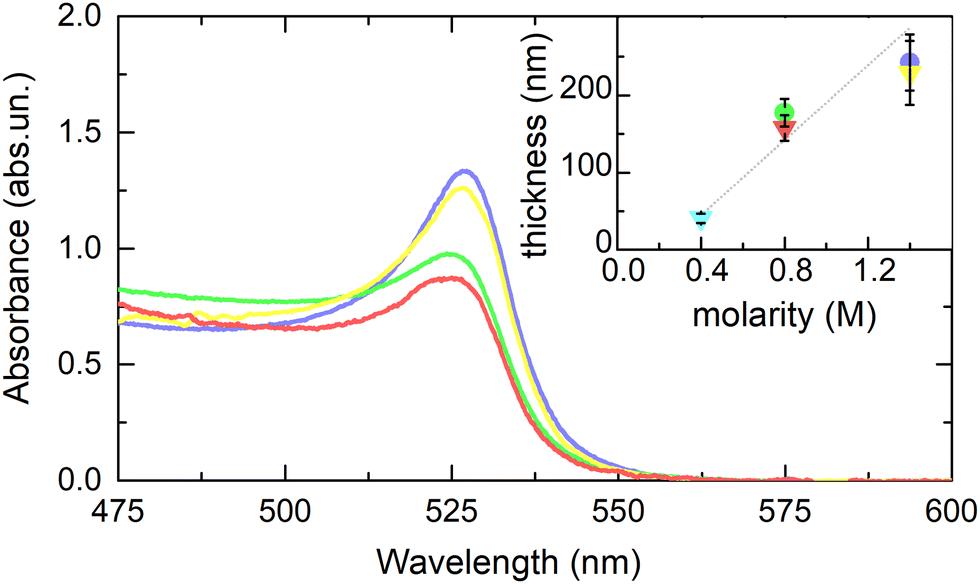 | ||
| Fig. 2 Average absorbance spectra measured on the 1.4 M and 0.8 M MAPbBr3 films on ITO and STO. Colour palette as in Fig. 1. In the inset, estimated thicknesses versus precursor molarity (circles: films on ITO; triangles: films on STO; error bars are estimated based on the dispersion in repeated optical measurements and the uncertainty on the absorption coefficient). The fitted linear trend is shown (dotted gray line). | ||
3.2 Physical degradation
To study the degradation processes and their typical timescale, four total freshly prepared films of MAPbBr3 (1.4 M) deposited on STO and ITO were stored at ambient temperature in a N2 filled, sealed vial at atmospheric pressure, and in vacuum (at pressure maintained at P = 13 mbar by continuous pumping). In addition, a film prepared with 0.8 M precursor concentration deposited on ITO was also stored in vacuum atmosphere; the results of its analysis are reported in Section S3 of the ESI.† No shielding for ambient optical radiation was implemented, to mimic relevant material application conditions. The deterioration of the films was monitored by optical and fluorescence microscopy, and Raman spectroscopy. The optical microscopy images of the samples (acquired in reflectance mode) at different timesteps from deposition are shown in Fig. 3. As reasonably expected, the freshly prepared samples evenly cover the substrates and show no sign of deterioration, even at the largest magnification available (zoom in Fig. 3(a), (d), (g) and (j)). After storing the films for some time both under vacuum and nitrogen atmosphere, physical degradation can be observed on all samples, with the formation of small yellow crystallites of size between 1–5 μm (Fig. 3(b), (e), (h) and (k)). A visual inspection of the image in Fig. 3(c) and (i) shows the bare surface of the ITO and STO substrates (appearing in gray), as evidence that the physical degradation of the perovskite film is developing under vacuum. On the other hand, N2 storage only slightly affects the film integrity and at a much slower rate (after approximately a month, see Fig. 3(f) and (l)). To explain the observed behavior, we first consider that all the films analyzed in this paper are polycrystalline, with an expected fine grain structure and a consequently a large number of grain boundary interfaces.31 It is known that an intergranular film is typically formed in between the grains, with a different structure (e.g., amorphous) and chemical composition (e.g., containing residual solvent) as compared to the HOIP domains. The grain size is expected to be smaller than the spatial resolution of the optical techniques here employed (∼1 μm), thus making the grain boundary indistinguishable optically, but readily observable by high resolution microscopies like SEM (see Fig. S4, ESI†).31,32 The literature allows to hypothesize a physical degradation mechanism triggered by the polycrystalline nature of the sample. Unfortunately, the composition of the intergranular film is not assessable by Raman scattering, as the scattering volume is mostly occupied by the bulky grains, providing the largest part of the Raman signal. Nevertheless, the intergranular film is expected to show different physical–chemical properties compared to the HOIP grains, resulting in a lower chemical stability and higher susceptibility to moisture degradation.31,32 The origin of microcrystal formation (Fig. 3) can be thus hypothesized based on the evaporation of the MA molecules and the possible solvent residues embedded in the intergranular film, more likely occurring in vacuum. The evaporation produces an unbalance in the forces acting on each crystallite in the film, resulting in its morphological instability and finally leading to the formation of larger grains,32 with a new equilibrium shape31 governed by minimization of the sum of the elastic and surface energy,33,34 and the consequent macroscopic fragmentation of the HOIP thin film. Thus, storing the films at 13 mbar (i.e., in vacuum) strongly accelerates the natural degradation of the samples. | ||
| Fig. 3 Optical microscopy images of MAPbBr3 (1.4 M) film deposited on: (a) and (d) ITO, and (g) and (j) STO. Images of the films: (b) and (h) stored in 13 mbar vacuum for two weeks; (c) and (i) stored in 13 mbar vacuum for three weeks; (e) and (k) stored in N2 atmosphere for one week and (f) and (l) one month. Images were acquired with 20× (left column) and 100× magnification. | ||
The Raman spectra acquired on the microcrystals of all three samples are shown in Fig. 4 and are compared with the ones acquired on freshly made films (these are obtained by subtracting the Raman spectra of bare substrates to the sample ones, see Fig. 4(a)) and to that of a pristine MAPbBr3 powder sample, as reported by F. Capitani et al.35 In the low Raman shift region, all the spectra look comparable, and the fitting deconvolution of the spectral profiles gives similar results. The Raman spectra of the pristine film samples on both STO and ITO substrates is covered by the substrate signals, particularly in the MA fingerprint region, above 900 cm−1 (Fig. 4(a)). On the contrary, the Raman spectra of the microcrystals reveal the vibrational modes of the MA molecule, as shown in Fig. 4(c) and (d). This evidence suggests that the microcrystal thickness is sufficiently large to screen any light emitted by the substrate, and that these domains reasonably form from film aggregation, as discussed above, with no change of chemical composition in the sample. In other words, the physical degradation of the film results in the clustering of the sample into more compact crystalline aggregates which are stabilized for the decrease of the contact area with the substrate (minimization of surface tension). This is not accompanied by any relevant changes in the chemical or crystal structure. After three weeks of vacuum storage, the MAPbBr3 films show further signs of physical degradation, as shown in Fig. 3(c), and the perovskites microcrystals also gather in larger clusters (contraction effect).22
 | ||
| Fig. 4 (a) Raman spectra of the MAPbBr3 films (black lines) and of the bare ITO and STO substrates (gray lines). (b) Raman spectra, in the low Raman shift (0–400 cm−1) range, of the MAPbBr3 microcrystals formed on the aged samples, compared to the Raman spectrum of pristine MAPbBr3 powder (from ref. 35) and to those obtained subtracting the substrate background to the thin film Raman spectra. In panel (b), the dashed gray lines show the spectral deconvolution in Gaussian components, centered at the vibrational modes reported by O. Yaffe et al.36 (c) Raman spectra of the microcrystals in the 1300–1700 cm−1 and (d) in the 2800–3100 cm−1 range. All Raman spectra in panels b, c and d are normalized to the intensity of the lowest frequency mode (∼15 cm−1). | ||
3.3 Chemical degradation
Beside the purely physical degradation consisting in the shrinking of the deposit, chemical degradation also occurs in the samples stored under vacuum. Instead, no signs of chemical degradation occurring in the analyzed time window could be detected on the sample stored under N2, where the measured Raman signals were homogeneous and consistent with that of the pristine film. For sake of simplicity, only the results from the 0.8 M MAPbBr3 film on ITO will be discussed. Analogous observations are valid also for the other samples stored in vacuum, on both STO and ITO (see Section S4 of the ESI†). After two weeks of storage under vacuum, the MAPbBr3 film appears extremely fragmented. In some regions, big crystalline aggregates (linear size 10–20 μm), larger than those shown in Fig. 3 and above discussed, developed with a different optical appearance (see Fig. 5).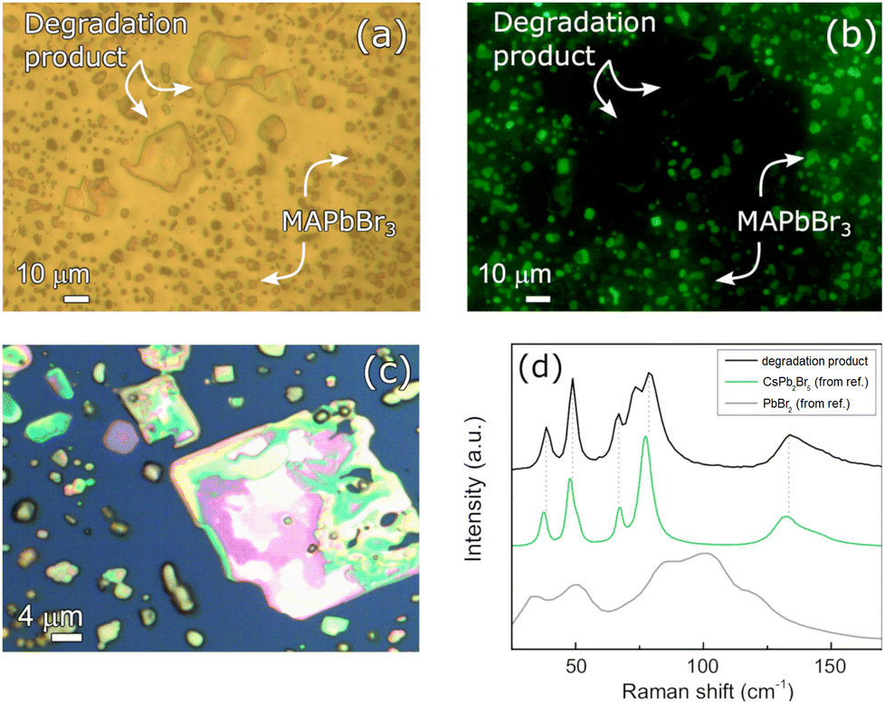 | ||
| Fig. 5 Transmission optical microscopy and fluorescence microscopy images on the same area of the 0.8 M MAPbBr3 film on ITO after vacuum storage. Images were acquired with (a) broadband and (b) blue light (380–500 nm) illumination, respectively. (c) Optical microscopy image after two weeks of storage under vacuum acquired with 100× magnification (reflectance mode). A large crystal is observed, and it is reasonably associated with a degradation product owing to its appearance and optical properties. (d) Raman spectrum of the large crystal shown in (c) at low Raman shift (black line). Comparison with the Raman spectrum of precursors and plausible degradation products PbBr2 (grey line, from ref. 37) and CsPb2Br5 (green line, from ref. 38). | ||
Upon comparison of the transmission optical and fluorescence microscopy images in Fig. 5(a) and (b), it is concluded that these new aggregates are not made of MAPbBr3. The image in (b) was obtained by illuminating the sample with blue light, above MAPbBr3 bandgap absorption (Fig. 2). A fragmented MAPbBr3 film should still emit fluorescence light with above bandgap irradiation, as shown in Fig. 1(e)–(h). On the other hand, the new crystal domains are absent in the fluorescence image: their emission properties are then different from that of MAPbBr3, and this likely points to domains with distinct chemical composition or structure. To identify the produced degradation compounds, we studied the Raman spectrum of the crystallites. As shown in Fig. 5(d), the Raman spectrum does not resemble the one of MAPbBr3, nor the one of the solid precursors PbBr2 used for the synthesis of the compound. A plausible hypothesis for the nature of these domains can be formulated referring to the structural phase transitions of the inorganic perovskite CsPbBr3. It is known from the literature that CsPbBr3 can decompose into the solid byproduct CsPb2Br5 when exposed to a humid environment: H2O molecules permeate the solid and strip CsBr out of the crystal, changing the coordination number of Pb(II) and inducing a phase transition.39 Furthermore, as reported in the work of W. Guo et al.,40 X-ray diffraction (XRD) measurements showed that subjecting MAPbBr3 to the simultaneous stressing action of high temperature and intense UV irradiation led to the formation of NH4Pb2Br5, a compound with the same room-temperature structure of CsPb2Br5 (as shown in the insets of Fig. 6). With these premises, we hypothesize that this degradation product might result as well by simply storing MAPbBr3 films under vacuum conditions. To the best of our knowledge, that is an original and unreported observation.
 | ||
| Fig. 6 (a) Fitting deconvolution of the Raman spectrum of CsPb2Br5 measured by V. G. Hadjiev et al.38 (b) Fitting deconvolution of the Raman spectrum of NH4Pb2Br5 measured in this work. In the insets, the layered crystal structures of CsPb2Br5 (a) and NH4Pb2Br5 (b). Images produced with the VESTA software. | ||
Given the very low amount and the dispersed character of the new degradation product NH4Pb2Br5 over the surface of the degraded film, an XRD analysis on these samples is not expected to give satisfactory results neither in the detection, nor in the identification of the new material, even in the grazing angle mode. To the best of our knowledge, degradation and/or defective products cannot be easily detected in thin films by XRD at volume fractions below 10%.41,42 On the contrary, Raman and photoluminescence (i.e., optical) studies allow to overcome that limit.5 In the present case, the volume fraction of the degradation product, as estimated from microscopy imaging, is in the order of a few percent (<5%), and hence would not provide the necessary contrast in an XRD analysis. On the other hand, a possible elemental determination by energy dispersive X-ray analysis would not be indicative of the structure of the degradation product, and it would retrieve nearly the same composition of the perovskite, that differs to NH4Pb2Br5 for the sole additional presence of C atoms. We thus believe the vibrational fingerprint provided by Raman spectroscopy, and the comparison to the literature data, is the most informative option for the identification of the degradation products.
In NH4Pb2Br5, the Pb2+ cations coordinate eight Br− anions (and not six with octahedral geometry as in the perovskite structure), forming a compact layer of face-sharing [Pb2Br5]− hendecahedric units. Each layer is separated by a layer of NH4+ (or Cs+) cations to form NH4Pb2Br5 (or CsPb2Br5) with resulting formation of a layered intercalation compound.43 Further confirmation of the similarity between the two crystal structures is given by the relative ease in substituting the NH4+ with Cs+ ions by just adding NH4Pb2Br5 powder in a CsBr methanol solution. This exchange turns the first compound into the second.44 The comparison of the Raman spectra collected on the crystalline aggregates with that of CsPb2Br5,38,45,46 whose phonon peaks are associated solely with the vibrational modes of the hendecahedric units (identical for the two compounds), allowed us to identify the observed vibrational modes of Fig. 5(d). The Raman spectra of CsPb2Br5 and NH4Pb2Br5, shown separately in Fig. 6, were deconvoluted using Gaussian and Lorentzian peak functions (for the assessed peak frequencies, see Table 1).
| NH4Pb2Br5 peak position (cm−1) | CsPb2Br5 peak position (cm−1) |
|---|---|
| 38 | 37 |
| 48 | 48 |
| 64 | 67 |
| 72 | |
| 79 | 77 |
| 134 | 132 |
| 143 | 140 |
In Section S5 of the ESI,† we report two possible alternative pathways for the fomation of NH4Pb2Br5 from MAPbBr3 under vacuum conditions, one of which is triggered by above bandgap illumination. As no direct assessment of the intermediate (mostly, gaseous) reaction products can be realized with the methods here employed, we refer to the processes merely as hypotheses, which deserve further investigation.
After three weeks, the sample stored under vacuum show considerable signs of degradation. Both MAPbBr3 microcrystals and NH4Pb2Br5 aggregates are largely present on the substrates surface and the NH4Pb2Br5 aggregates appear larger in size as compared to the ones observed at the two weeks’ timestamp. This increase in scale could be probably attributed to aggregation mechanisms analogous to the ones originally observed for the MAPbBr3 microcrystals.
4 Conclusions
In this work we analyzed the physical and chemical stability of MAPbBr3 thin film deposited on SrTiO3 (STO) and In2−xSnxO3 (ITO) substrates under different storage conditions. Film samples deposited with different precursors molarities (0.4 M, 0.8 M and 1.4 M) were first analyzed as a reference after storage in air. UV-Vis absorption spectroscopy was employed to infer the mean thicknesses of each sample, and optical microscopy was used to evaluate the overall film quality. Microscopy images acquired on these samples showed that the thicker films (∼300 nm) develop a wrinkled surface pattern with spatial period of 2.5 μm, as an effect of the compressive stress endured by the film during the spin coating synthesis process. Films on STO and ITO were analyzed upon storage under N2 atmosphere, or under vacuum at 13 mbar. All the samples showed signs of physical degradation with the appearance of micrometric-sized MAPbBr3 crystals on the surface. N2 atmosphere preserved the integrity of the film for a month (indeed, only a few microcrystals appeared on the sample), while vacuum accelerated the degradation process with observation of film fragmentation just a week after deposition. Aggregates of the byproduct NH4Pb2Br5 were also retrieved in the samples stored under vacuum, suggesting that chemical degradation also occurred. Likely, chemical degradation was caused by the volatility of MA. Two possible degradation routes were proposed for the formation of NH4Pb2Br5. Joint Raman and microscopy techniques allowed us to perform nondestructive and informative measurements on the film surfaces with accurate spatial resolution, providing an unambiguous identification of the degradation pathways. For the characterization of the species produced in the degradation process of HOIPs, we demonstrate that the experimental approach here presented results in a possibly more informative characterization when compared to the prevalent AFM/SEM and UV-Vis approaches reported in the literature. In conclusion, this work provides insights on the degradation mechanisms of thin perovskite films as a function of thickness and storage conditions. Storing the films either in air, N2 or vacuum provided very different outcomes for the film integrity, from both a physical and a chemical point of view. The observation of microcrystals and aggregates of completely different chemical structure allows to understand mechanisms controlling the long-term stability/degradation of HOIPs. The present observations can provide a valuable contribution to the study of the environmental stability of HOIP films and useful insights on the ideal working condition of these systems.Author contributions
V. C. and F. M. performed the measurements and the data analysis. V. C. wrote the main draft. J. B. synthesized the samples. C. F., D. D., A. N., F. M., P. P., and C. P. contributed to the interpretation of the results and critically reviewed the paper. C. F. conceived and supervised the work. All the authors discussed the results and revised the article. All authors have given approval to the final version of the manuscript.Data availability
Data for this article, in the form of microscopy images and txt files of the spectra in the paper are available at Zenodo at [https://doi.org/10.5281/zenodo.11639850].Conflicts of interest
There are no conflicts to declare.Acknowledgements
This research work was supported by the PERMIT project (Project ATENEO 2022, Prot. No. RM1221816BE09678) from Sapienza University of Rome. The project has been funded through the PNRR MUR projects PE0000023-NQSTI and ECS0000024-Rome Technopole financed by the European Union NextGenerationEU. J. B., and F. M. acknowledge the European Union's Horizon 2020 research and innovation programme under Grant Agreement No 101007084 (CITYSOLAR). P. P. and C. F. acknowledge financial support for the optical spectroscopy measurements from Regione Lazio, L. R. 13/2008, Progetto SOSpESO, N.Prot. A0375-2020-36622.Notes and references
- T. Zuo, X. He, P. Hu and H. Jiang, ChemNanoMat, 2019, 5, 278–289 Search PubMed.
- L. Protesescu, S. Yakunin, M. I. Bodnarchuk, F. Krieg, R. Caputo, C. H. Hendon, R. X. Yang, A. Walsh and M. V. Kovalenko, Nano Lett., 2015, 15, 3692–3696 Search PubMed.
- J. H. Noh, S. H. Im, J. H. Heo, T. N. Mandal and S. I. Seok, Nano Lett., 2013, 13, 1764–1769 Search PubMed.
- M.-C. Tang, H. X. Dang, S. Lee, D. Barrit, R. Munir, K. Wang, R. Li, D.-M. Smilgies, S. De Wolf and D.-Y. Kim, et al. , Sol. RRL, 2021, 5, 2000718 Search PubMed.
- V. Carpenella, F. Ripanti, E. Stellino, C. Fasolato, A. Nucara, C. Petrillo, L. Malavasi and P. Postorino, J. Phys. Chem. C, 2023, 127, 2440–2447 Search PubMed.
- T. M. Brenner, D. A. Egger, L. Kronik, G. Hodes and D. Cahen, Nat. Rev. Mater., 2016, 1, 1–16 Search PubMed.
- Best Research-Cell Efficiency Chart, 2024, https://www.nrel.gov/pv/cell-efficiency.html [Accessed: (24-03-2024)].
- X. Y. Chin, D. Turkay, J. A. Steele, S. Tabean, S. Eswara, M. Mensi, P. Fiala, C. M. Wolff, A. Paracchino and K. Artuk, et al. , Science, 2023, 381, 59–63 Search PubMed.
- A. M. Leguy, Y. Hu, M. Campoy-Quiles, M. I. Alonso, O. J. Weber, P. Azarhoosh, M. Van Schilfgaarde, M. T. Weller, T. Bein and J. Nelson, et al. , Chem. Mater., 2015, 27, 3397–3407 Search PubMed.
- J. A. Christians, P. A. Miranda Herrera and P. V. Kamat, J. Am. Chem. Soc., 2015, 137, 1530–1538 Search PubMed.
- A. D. Sheikh, A. Bera, M. A. Haque, R. B. Rakhi, S. Del Gobbo, H. N. Alshareef and T. Wu, Sol. Energy Mater. Sol. Cells, 2015, 137, 6–14 Search PubMed.
- I. Deretzis, E. Smecca, G. Mannino, A. La Magna, T. Miyasaka and A. Alberti, J. Phys. Chem. Lett., 2018, 9, 3000–3007 Search PubMed.
- N. Aristidou, I. Sanchez-Molina, T. Chotchuangchutchaval, M. Brown, L. Martinez, T. Rath and S. A. Haque, Angew. Chem., 2015, 127, 8326–8330 Search PubMed.
- R. Guo, D. Han, W. Chen, L. Dai, K. Ji, Q. Xiong, S. Li, L. K. Reb, M. A. Scheel and S. Pratap, et al. , Nat. Energy, 2021, 6, 977–986 Search PubMed.
- I. Deretzis, A. Alberti, G. Pellegrino, E. Smecca, F. Giannazzo, N. Sakai, T. Miyasaka and A. La Magna, Appl. Phys. Lett., 2015, 106, 131904 Search PubMed.
- A. Alberti, I. Deretzis, G. Pellegrino, C. Bongiorno, E. Smecca, G. Mannino, F. Giannazzo, G. G. Condorelli, N. Sakai and T. Miyasaka, et al. , ChemPhysChem, 2015, 16, 3064–3071 Search PubMed.
- M. Pugliese, F. Bisconti, A. Rizzo, S. Colella, C. T. Prontera, G. Gigli, V. Maiorano and P. Cossari, ACS Appl. Energy Mater., 2020, 3, 10453–10462 Search PubMed.
- S. Liu, Y. W. Du, C. Y. Tso, H. H. Lee, R. Cheng, S.-P. Feng and K. M. Yu, Adv. Funct. Mater., 2021, 31, 2010426 Search PubMed.
- Y. Du, S. Liu, Z. Zhou, H. H. Lee, T. C. Ho, S.-P. Feng and C. Y. Tso, Mater. Today Phys., 2022, 23, 100624 Search PubMed.
- H. Mehdi, A. Mhamdi, R. Hannachi and A. Bouazizi, RSC Adv., 2019, 9, 12906–12912 Search PubMed.
- K. A. Bush, N. Rolston, A. Gold-Parker, S. Manzoor, J. Hausele, Z. J. Yu, J. A. Raiford, R. Cheacharoen, Z. C. Holman and M. F. Toney, et al. , ACS Energy Lett., 2018, 3, 1225–1232 Search PubMed.
- M. C. Cross and P. C. Hohenberg, Rev. Mod. Phys., 1993, 65, 851 Search PubMed.
- D. Dini, K. Doblhofer and G. Ertl, Phys. Chem. Chem. Phys., 2000, 2, 1183–1186 Search PubMed.
- S.-G. Kim, J.-H. Kim, P. Ramming, Y. Zhong, K. Schötz, S. J. Kwon, S. Huettner, F. Panzer and N.-G. Park, Nat. Commun., 2021, 12, 1554 Search PubMed.
- A. Tejada, S. Braunger, L. Korte, S. Albrecht, B. Rech and J. Guerra, J. Appl. Phys., 2018, 123, 175302 Search PubMed.
- S. Braunger, L. E. Mundt, C. M. Wolff, M. Mews, C. Rehermann, M. JosÌŒt, A. Tejada, D. Eisenhauer, C. Becker and J. A. Guerra, et al. , J. Phys. Chem. C, 2018, 122, 17123–17135 Search PubMed.
- S. Jariwala, H. Sun, G. W. Adhyaksa, A. Lof, L. A. Muscarella, B. Ehrler, E. C. Garnett and D. S. Ginger, Joule, 2019, 3, 3048–3060 Search PubMed.
- A. Bercegol, F. J. Ramos, A. Rebai, T. Guillemot, J.-B. Puel, J.-F. Guillemoles, D. Ory, J. Rousset and L. Lombez, J. Phys. Chem. C, 2018, 122, 23345–23351 Search PubMed.
- A. M. Leguy, P. Azarhoosh, M. I. Alonso, M. Campoy-Quiles, O. J. Weber, J. Yao, D. Bryant, M. T. Weller, J. Nelson and A. Walsh, et al. , Nanoscale, 2016, 8, 6317–6327 Search PubMed.
- V. Carpenella, C. Fasolato, D. Di Girolamo, J. Barichello, F. Matteocci, C. Petrillo, D. Dini and A. Nucara, J. Phys. Chem. C, 2023, 127, 22097–22104 Search PubMed.
- Q. Wang, B. Chen, Y. Liu, Y. Deng, Y. Bai, Q. Dong and J. Huang, Energy Environ. Sci., 2017, 10, 516–522 Search PubMed.
- F. Zhang, J. Cong, Y. Li, J. Bergstrand, H. Liu, B. Cai, A. Hajian, Z. Yao, L. Wang and Y. Hao, et al. , Nano Energy, 2018, 53, 405–414 Search PubMed.
- P. Müller and A. Saúl, Surf. Sci. Rep., 2004, 54, 157–258 Search PubMed.
- S. Tamulevičius, Vacuum, 1998, 51, 127–139 Search PubMed.
- F. Capitani, C. Marini, S. Caramazza, P. Dore, A. Pisanu, L. Malavasi, L. Nataf, F. Baudelet, J.-B. Brubach and P. Roy, et al. , J. Phys. Chem. C, 2017, 121, 28125–28131 Search PubMed.
- O. Yaffe, Y. Guo, L. Z. Tan, D. A. Egger, T. Hull, C. C. Stoumpos, F. Zheng, T. F. Heinz, L. Kronik and M. G. Kanatzidis, et al. , Phys. Rev. Lett., 2017, 118, 136001 Search PubMed.
- B. Akbali, G. Topçu, T. Guner, M. Ozcan, M. M. Demir and H. Sahin, Phys. Rev. Mater., 2018, 2, 034601 Search PubMed.
- V. Hadjiev, C. Wang, Y. Wang, X. Su, H. Calderon, F. R. Hernandez, Z. Wang and J. Bao, J. Phys.: Condens. Matter, 2018, 30, 405703 Search PubMed.
- M. Liu, J. Zhao, Z. Luo, Z. Sun, N. Pan, H. Ding and X. Wang, Chem. Mater., 2018, 30, 5846–5852 Search PubMed.
- W. Guo, N. Chen, B. Xu, Y. Lu, B. Li, T. Wu, Q. Cheng, Y. Li, J. Chen and Y. Lin, et al. , Nanomaterials, 2019, 9, 1158 Search PubMed.
- G. Abdelmageed, L. Jewell, K. Hellier, L. Seymour, B. Luo, F. Bridges, J. Z. Zhang and S. Carter, Appl. Phys. Lett., 2016, 109, 233905 Search PubMed.
- D. M. Berg, M. Arasimowicz, R. Djemour, L. Gütay, S. Siebentritt, S. Schorr, X. Fontané, V. Izquierdo-Roca, A. Pérez-Rodriguez and P. J. Dale, Thin Solid Films, 2014, 569, 113–123 Search PubMed.
- S. M. Whittingha, Intercalation chemistry, Elsevier, 2012 Search PubMed.
- X. Wang, D. Zhang, C. Gao, F. Qiao, J. Liang, H. Liu and W. Shen, ACS Appl. Energy Mater., 2022, 5, 10897–10906 Search PubMed.
- C. Wang, Y. Wang, X. Su, V. G. Hadjiev, S. Dai, Z. Qin, H. A. Calderon Benavides, Y. Ni, Q. Li and J. Jian, et al. , Adv. Mater., 2019, 31, 1902492 Search PubMed.
- X. Wu, X. Zhang, W. Yu, Y. Zhou, W. Wong, W. He, K. P. Loh, X.-F. Jiang and Q.-H. Xu, J. Mater. Chem. A, 2023, 11, 4292–4301 Search PubMed.
Footnotes |
| † Electronic supplementary information (ESI) available: Additional data are available on (S1) scattering background in the optical extinction spectra; (S2) characterization of the 0.4 M MAPbBr3 film on STO; (S3) physical degradation of the 0.8 M MAPbBr3 film on ITO, in vacuum; (S4) chemical degradation of MAPbBr3 film on STO. See DOI: https://doi.org/10.1039/d4cp01509f |
| ‡ These authors contributed equally to this work. |
| This journal is © the Owner Societies 2024 |