
 Open Access Article
 This Open Access Article is licensed under a
 Creative Commons Attribution 3.0 Unported Licence
Contactless analysis of surface passivation and charge transfer at the TiO2–Si interface†
Ramsha
Khan‡
 a,
Xiaolong
Liu‡
b,
Ville
Vähänissi
b,
Harri
Ali-Löytty
c,
Hannu P.
Pasanen
a,
Hele
Savin
*b and
Nikolai V.
Tkachenko
*a
a,
Xiaolong
Liu‡
b,
Ville
Vähänissi
b,
Harri
Ali-Löytty
c,
Hannu P.
Pasanen
a,
Hele
Savin
*b and
Nikolai V.
Tkachenko
*a
aPhotonic Compounds and Nanomaterials Group, Faculty of Engineering and Natural Sciences, Tampere University, Tampere University, P.O. Box 541, FI-33014, Finland. E-mail: nikolai.tkachenko@tuni.fi
bDepartment of Electronics and Nanoengineering, Aalto University, Tietotie 3, Espoo 02150, Finland. E-mail: hele.savin@aalto.fi
cSurface Science Group, Faculty of Engineering and Natural Sciences, Tampere University, Tampere University, P.O. Box 692, FI-33014, Finland
First published on 3rd May 2024
Abstract
Transition metal oxides are pivotal in enhancing surface passivation and facilitating charge transfer (CT) in silicon based photonic devices, improving their efficacy and affordability through interfacial engineering. This study investigates TiO2/Si heterojunctions prepared by atomic layer deposition (ALD) with different pre-ALD chemical and post-ALD thermal treatments, exploring their influence on the surface passivation and the correlation with the CT at the TiO2–Si interface. Surface passivation quality is evaluated by the photoconductance decay method to study the effective carrier lifetime, while CT from Si to TiO2 is examined by transient reflectance spectroscopy. Surprisingly, the as-deposited TiO2 on HF-treated n-Si (without interfacial SiOx) demonstrates superior surface passivation with an effective lifetime of 1.23 ms, twice that of TiO2/SiOx/n-Si, and a short characteristic CT time of 200 ps, tenfold faster than that of TiO2/SiOx/n-Si. Post-ALD annealing at temperatures approaching the TiO2 crystallization onset re-introduces the SiOx layers in HF-treated samples and induces chemical and structural changes in all the samples which decrease passivation and prolong the CT time and are hence detrimental to the photonic device performance.
1. Introduction
Efficiently harnessing renewable energy is crucial, and silicon's (Si) abundance on Earth, coupled with its favorable 1.1 eV band gap, allows it to operate effectively within the visible to NIR range of the solar spectrum.1–3 As a result, it has become a fundamental component in photovoltaic (PV) cells4,5 and photoelectrochemical (PEC) cells.6,7 Among these, crystalline silicon (c-Si) based devices have emerged as highly attractive and promising devices for cost-effective, green, and sustainable renewable energy production. However, the performance of state-of-the-art c-Si-based PV and PEC devices is often limited by recombination of their surfaces and interfaces which leads to a loss in their photogenerated charge carrier collection and thus a reduction in their energy conversion efficiency. The reduction of such recombination, commonly referred to as surface passivation, can be achieved by the combined effect of the reduction in the trap states present at the surface via a chemical component, and the reduction in the charge carriers available for a recombination process via a field effect component.8 Passivating layers have demonstrated significant potential in enhancing the performance of c-Si solar cells, enabling their theoretical efficiency limit to approach approx. 29.43%.9–11Transition metal oxides (TMOs) including ZnO, MoO3, WO3, V2O5, TiO2, and CuO have attracted great interest as potential passivating layers for silicon surfaces and interfaces, offering tunable optoelectronic properties with cost-effective deposition methods.12–16 Sahoo et al. deposited 1 nm CuO as a tunneling oxide passivating layer over Si and improved the minority carrier lifetime of the Si-based solar cells.14 Gerling et al. deposited MoO3, WO3 and V2O5, over n-Si and improved the lifetime of carriers up to 240, 142, and 4.5 μs, respectively.17 Loo et al. deposited a 75 nm ZnO film over n-Si by ALD and improved the carrier lifetime up to 312 μs.18 However, among them one promising material is TiO2 which has excellent chemical stability, dielectric properties, and high transparency that reduce problems such as surface parasitic absorbance.19,20 Atomic layer deposition (ALD) has emerged as a powerful method to grow TiO2 thin films on Si substrates for passivation application.21–23 It has been employed extensively since it allows growth of pinhole-free high quality TiO2 thin films at mono layer thickness with controllable and favorable optical properties.19,21,24,25 The properties of ALD TiO2 thin films can be affected by substrate pre-treatments, precursor choice, growth parameters and post-deposition treatments. Recent research has demonstrated that by depositing a TiO2 surface passivation layer on Si by ALD using TiCl4 and H2O precursors, the effective minority carrier lifetimes increase above 10 ms with decreasing ALD growth temperature, which is due to the increasing amount of ALD precursor traces (Cl and H) within TiO2 films as the growth temperature decreases.26 Previous studies show that the quality of surface passivation by amorphous TiO2 thin film is sensitive to Si wafer pre-treatments and thus can be significantly optimized and increased by applying precisely conditioned annealing, particularly through a pre-ALD growth of a SiOx interlayer.20,27–29 However, post-ALD deposition, the increased annealing temperature and duration can lead to a noticeable decline in surface passivation quality due to TiO2 crystallization and associated breaking of Si–O–Ti bonds at the TiO2–Si interface.28,29
In addition to surface passivation, TMOs can also be applied over Si as corrosion protection layers. In that case, meticulous attention should be paid to the ultra-fast charge transfer (CT) (in the ps–ns time domain) from the semiconductor photoabsorber to the TMO coating, as it can significantly impact the performance of PV devices. In high-efficiency PV cells with passivating contacts, majority carriers traverse the passivating TMO layer to reach the metal contact, and similarly, in PEC cells, carriers navigate through the TMO layer to access the reactive surface. Since TiO2 exhibits hole-blocking and electron-transporting capabilities, it can be used simultaneously for surface passivation and CT in both PV and PEC devices.30–32 However, earlier studies often show a trade-off between the surface passivation and CT at the TiO2–Si interface. For example, the presence of a thin SiOx interfacial layer can improve the passivation quality but it limits the CT process.33–35 Therefore, investigating and understanding the CT dynamics of photoexcited charges from Si to TiO233,36 across the TiO2–Si interface is crucial for optimizing the design and performance of the devices that rely on these materials. Femtosecond transient reflectance (TR) spectroscopy is a time-resolved technique used to extract information about the population of photogenerated charge carriers. This technique allows us to map out charge-transfer pathways by identifying decay features in the spectra. Consequently, information about the quenching and transfer of charge carriers, along with their corresponding lifetimes, which is relevant to photonic applications, can be extracted within femtosecond to nanosecond timescales.37–39 Herein, we have employed TR spectroscopy to get a complete picture of the phenomena related to ultrafast changes in reflectivity, diffusion of carriers, and particularly the CT process occurring at the interface in our TiO2/Si heterojunctions.
In this study, we prepare high-quality ALD TiO2 thin films at 120 °C using TiCl4 and H2O precursors on both p- and n-type Si substrates, with different pre-ALD chemical and post-ALD thermal treatments. This ALD TiO2 coating is amorphous and contains an elevated amount of precursor traces (∼1 at% H and Cl).40 The post-ALD thermal treatments were carefully selected to control the diffusion of H, Cl, and O within the TiO2 while maintaining the amorphous phase. The resulting surface passivation quality of the TiO2/Si heterojunctions is studied using the contactless quasi steady state photoconductance (QSSPC) method to measure the minority carrier lifetime. Furthermore, to gain insights on the CT dynamics across the TiO2–Si interface and transport of electrons in the TiO2 layer, contactless TR spectroscopy is utilized. Additionally, a Kelvin-probe is applied to study the Si surface barrier with TiO2 and how it contributes to the surface passivation and the CT in TiO2/Si heterojunctions. The topography of the samples is analyzed with AFM to examine and understand the structural and compositional changes occurring within the TiO2 thin films as a result of annealing and further how these changes contribute to the surface passivation and the CT process. Our results provide new insights on engineering effective surface passivation with optimized CT at the TiO2–Si interface, thus, paving the way for achieving highly efficient Si-based PV and PEC devices.
2. Synthesis
Boron-doped (p-Si samples) and phosphorus-doped (n-Si samples) single-side-polished float-zone c-Si wafers (100 mm diameter, (100) orientation, 1–5 Ω cm resistivity, and 280 μm thickness) were used as substrates. Initially, all the wafers underwent thermal oxidation at 1050 °C to deactivate bulk defects.34,41 After removing the thermal oxide layer by a 1% HF dip, the wafers were subsequently cleaned using a standard process consisting of RCA1, HF dip, and RCA2. This resulted in a chemical SiOx surface layer42 with a thickness of 1.8 nm determined by ellipsometry, assuming a refractive index of 1.465 at 632.8 nm. However, this thickness is slightly overestimated and actual thickness should be thinner than <1 nm.43 Half of the samples were subjected to a second HF dip after the RCA2 step just before the ALD growth of TiO2 to prepare TiO2/Si samples without an interfacial SiOx layer.44,45 Saari et al. have previously found out by XPS that the TiO2/Si interface remains free from SiOx for the thermal ALD TiO2 process using TDMAT and H2O precursors at 100 °C.44Right after the chemical treatments, the samples were immediately transferred to the ALD chamber to deposit the TiO2 thin films on both sides of the wafers. The deposition was done by using a thermal ALD tool (Beneq TFS-500), which was pumped to vacuum, heated to 120 °C and stabilized for 1 hour before starting deposition. TiCl4 was employed as the Ti precursor and water (H2O) was employed as the oxidant.40 A single ALD cycle consisted of a 200 ms TiCl4 precursor pulse and a 150 ms H2O oxidant pulse, each followed by a 3 s N2 purge. The deposition rate was estimated to be 0.43 Å per cycle and in total 1200 cycles were used for depositing 54 nm thick films, as determined by ellipsometry and confirmed by SEM (Fig. S1, ESI†).
The thickness of the TiO2 films was optimized for TR measurements, in order to acquire a suitable interference pattern to increase the signal strength of transferred carriers while retaining the same interface and CT rate. The steady-state reflectance spectra of all the as-deposited TiO2/Si heterojunctions are shown in the ESI,† Fig. S2 confirming similarity of the samples, i.e., the HF-treatment had only little effect on the TiO2 film thickness.33 Full wafers were cut to quarters and then the samples were thermally annealed in a tube furnace (ATV PEO-601) under N2 ambience at 250 °C for 5, 10, and 15 minutes. Despite the HF treatment, some interfacial SiOx grows between Si and TiO2 during the thermal annealing process.29 Saari et al. have shown that the thickness of interfacial SiOx increases linearly with temperature in the range of 200–550 °C.44 However, one quarter from each wafer was left without the thermal annealing of the as-deposited (as-dep.) TiO2/Si heterojunctions, to study how the thermal annealing affects both the surface passivation and CT properties. A schematic of sample preparation is shown in Fig. 1. Similarly, to study the effect of increasing the annealing temperatures and durations, TiO2/Si heterojunctions were annealed at 300 °C for 5, 60, and 90 minutes while one sample was left without annealing (as-deposited).
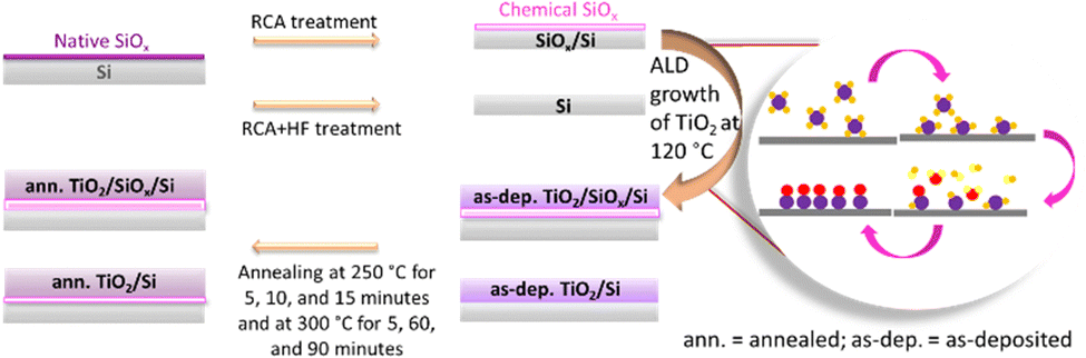 | ||
| Fig. 1 Synthesis of TiO2 on Si substrates by ALD using TiCl4 and H2O as precursor materials. | ||
3. Results and discussion
3.1. Surface passivation provided by TiO2
To study the passivation effect of TiO2 thin films on Si, effective carrier lifetimes, τeff, of both n-type and p-type silicon wafers with and without HF treatment are measured. Assuming that the bulk substrate has infinite lifetime, the upper limit of the surface recombination velocity (SRV), Seff,max, has been estimated. It can be defined as a rate at which carriers recombine at the surface and in the case of symmetrical samples it can be calculated as , where W is the wafer thickness.46Fig. 2a depicts typical injection-dependent effective lifetime results and the determined Seff,max for all the as dep. TiO2/Si and TiO2/SiOx/Si samples. Interestingly, the HF-treated as dep. samples exhibit higher lifetimes than their counterparts, the TiO2/SiOx/Si samples. Among all the samples, the TiO2/n-Si sample shows the best passivation performance having a maximum lifetime of approximately 1.23 ms. At a carrier injection level of 1.0 × 1015 cm−3, the corresponding Seff,max is around 11.4 cm s−1. This result is comparable to the values reported earlier for ALD TiO2 passivated silicon.26 Table S1 (ESI†) summarizes the lifetimes and the corresponding Seff,max for all the as-dep. TiO2/Si and TiO2/SiOx/Si samples.
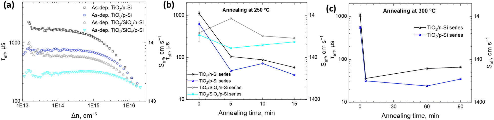 | ||
| Fig. 2 (a) Injection-level dependent effective lifetimes for Si wafers passivated by 54 nm thin films of (a) as-deposited TiO2, (b) annealed TiO2 films at 250 °C, and (c) annealed TiO2 films at 300 °C for different durations. The corresponding surface recombination velocities (Seff) are also shown on the right y-axis. | ||
The HF-treated as-dep. TiO2/p-Si shows a higher recombination rate of 20.3 cm s−1 as compared to the as-dep. TiO2/n-Si, which shows 11.4 cm s−1. For reference, for HF-treated (Si-H terminated/H passivated Si surface)47 n- and p-Si, the Seff,max values were 636.4 and 241.4 cm s−1, respectively. This means that with the deposition of TiO2 thin films, the Seff values are minimized for both n- and p-Si. The difference in Seff between n- and p-Si can be accounted for by different surface passivation properties, as the bulk of both substrates has been proven to be of high quality (τeff above 10 ms) in separate experiments using Al2O3 surface passivation.48,49 Therefore, the dopant type in Si is found to have a minor influence on the achievable passivation levels. Loo et al. also observed a minor influence of the dopant type on the achievable passivation levels.18 Moreover, the results reveal a consistent pattern where the presence of RCA2 oxide increases the SRV for both p-type and n-type wafers underscoring the detrimental impact of this oxide on the passivation performance, as listed in Table S1 (ESI†). This observed trend is consistent with prior research, e.g., carried out by Mochizuki et al.20 and Liao et al.,29 which attributes the increase in Seff, in the case of amorphous TiO2 coatings, to the increase in the interfacial defect density upon the formation of SiOx at the TiO2–Si interface already during the annealing at 250 °C. The SiOx layer can either introduce defect states and recombination, or it affects the total charge of the thin film and thus weakens field-effect passivation. This is contrary to the literature where the presence of a thin SiOx layer has been shown to improve the passivation.27,28
Earlier studies (summarized in Table S2, ESI†) have shown that the Si surface passivation quality by ALD TiO2 thin films depends on the post-deposition thermal treatment. Therefore, the impact of the annealing on the Seff of the samples is studied. The samples are annealed at 250 °C (Fig. 2b) and 300 °C (Fig. 2c) for different durations. The results show that the as-dep. TiO2 grown on both HF-treated p- and n-Si substrates results in the lowest SRV while the annealing significantly enhances the SRV for all the samples. However, with annealing, a thermally introduced interfacial SiOx layer forms in between the TiO2 and Si which seems to prevent the further degradation of the lifetime. This leads to a situation where actually after the annealing, the SRV for samples that initially had RCA2 SiOx at the interface is lower than the SRV for samples that initially had no SiOx at the TiO2–Si interface as shown in Fig. 2b. Furthermore, after annealing at 300 °C for extended durations up to 90 minutes, both HF-treated TiO2/n-Si and TiO2/p-Si samples show a similar increment in the SRV as shown in Fig. 2c. This observed trend is consistent with prior research, e.g., carried out by Mochizuki et al.20 and Liao et al.,29 which attributes the increase in the SRV in the case of amorphous TiO2 coatings to the increase in the interfacial defect density upon the formation of SiOx at the TiO2–Si interface already during thermal annealing at 250 °C. Therefore, it is evident that the surface passivation quality started to degrade already at the thermal treatment temperatures that were not sufficiently high to induce TiO2 crystallization but at a temperature where diffusion of the dopants and impurities typically precedes the phase transition. This was confirmed by the Raman spectra of the samples after ALD and after 300 °C 90 min annealing (Fig. S10, ESI†) where no TiO2 crystalline peaks (anatase or rutile) are observed. It is suggested that impurities in the ALD TiO2 film originating from the ALD precursors, especially H can have a significant effect on the surface passivation.29,40
Fig. 3 presents measurements of the Si surface barrier height (Vsb) using the Kelvin-probe method after varying annealing temperatures and durations. In TiO2/n-Si sample series, both with and without HF-treatment, a strong negative Vsb is obtained which remains stable even when the samples are annealed at 300 °C up to 90 minutes. Conversely, for TiO2/p-Si sample series, both with and without an HF-treatment, Vsb is slightly negative initially and then increases to slightly positive values as the annealing duration is increased. These differences in Vsb values reflect the different electronic structures in p- and n-type Si.50 This happens as the Fermi-levels are closely aligned for p-Si and TiO2 which causes small Vsb, whereas the alignment of Fermi-levels for n-Si and TiO2 causes a notable upward band bending, as indicated by the high negative Vsb values. The notable upward band bending should be harmful for electron transport into TiO2 from Si and even result in a depletion of electrons at the n-Si surface, forming a hole-rich layer. The lowest SRV observed in Fig. 2 for HF-treated as-dep. TiO2/n-Si can be attributed to the strong field effect (inversion) passivation, whereas there is nearly no surface band bending on p-Si. This, coupled with the measured favorable lifetimes and low SRVs, indicates that all the as-dep. TiO2 thin films have a good chemical passivation quality for both p- and n-Si substrates. The values without any annealing in Fig. 3a and b are slightly different because they are from different runs of experiments and the differences are within the given error limits. However, the measured Vsb remains at a similar level after the thermal treatment with increased temperature and duration. The increase of absolute Vsb values observed in certain cases, such as the annealing of the TiO2/n-Si sample for 5 minutes, suggests an enhancement in field-effect passivation. However, despite this improvement, the SRV experiences a significant increment. This implies that the increased SRV may stem from thermally induced interfacial defects rather than alterations in field-effect passivation.
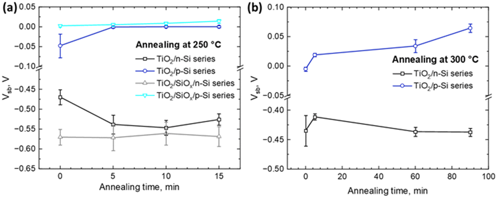 | ||
| Fig. 3 Surface barrier height of different series of TiO2/Si heterojunctions deposited at 120 °C and further annealed at (a) 250 °C and (b) 300 °C for different time durations. | ||
3.2. Charge transfer through the TiO2/Si interface
For optimal device performance, most of the minority carriers should remain in Si and there should be only majority charge carrier transfer across the TiO2–Si interface. Therefore, to carefully analyze the charge transfer from Si to TiO2 across the interface, contactless TR spectroscopy is utilized. Using this technique, one can measure the change in reflectance of the films upon photoexcitation. The samples were excited at 500 nm (with an energy density of 200 μJ cm−2) from the polished side of the samples to selectively generate the photocarriers in Si since TiO2 does not absorb light in the visible region of the solar spectrum. The photogenerated carrier density can be calculated using N0 = I × α × e−αx, where I is the intensity of the incoming light, α is the absorption coefficient, and x is the thickness at which the photocarriers are generated.33 Therefore, at 500 nm excitation, approximately 4.8 × 10⁹ e−/h+ pairs are generated at a depth of 1 μm in Si. The total measured signal in the case of this study is given by TRtotal = TRSi + TRTiO2.However, at 500 nm excitation, only Si is excited and any TRTiO2 signal must originate from the carriers transferred from Si to TiO2, and hence is termed as the “CT signal”. This signal is thus calculated by subtracting the estimated Si signal from the measured total signal. To examine how the charge carriers behave in Si upon photoexcitation at 500 nm, the temporal evolution of the TR spectra is observed for both pure Si substrates and TiO2/Si samples. Since the electron transfer from Si to the TiO2 layer is investigated, we focus mainly on samples with the n-Si substrate where electrons are the majority carriers. Hence, the TR spectra of both HF-treated pure n-Si substrate and as-dep. TiO2/n-Si samples are measured with excitation at 500 nm and the results are presented in the form of 2D maps as shown in Fig. 4a and b, respectively. For bare n-Si substrate, the TR spectra exhibit signals only in the positive range which decay as carriers diffuse from the surface to the bulk. However, with the addition of a 54 nm thick TiO2 thin film on Si, the interference pattern changes which in turn changes the TR spectra. Therefore, in the case of TiO2/n-Si samples, at longer delay times, >500 ps, the negative TR signal recovers partially and shows a blue shift while the positive TR signal starts evolving in the red region (600–750 nm) from 100 ps–5 ns in as-dep. TiO2/n-Si.
 | ||
| Fig. 4 Excitation of samples at 500 nm with 200 μJ cm−2 to obtain (a) TR spectra of the HF-treated bare n-Si substrate at different delay times, (b) TR spectra of the HF-treated as-dep. TiO2/n-Si sample at different delay times, (c) extracted CT spectra in the HF-treated as-dep. TiO2/n-Si sample where the arrows indicate electrons moving from n-Si to TiO2, and (d) comparison of the extracted CT spectra for the HF-treated as-dep. TiO2/n-Si sample and as-dep. TiO2/SiOx/n-Si at different delay times. | ||
To conduct a detailed analysis of the CT, we extract the TR spectra only related to the changes in TiO2 as a result of the CT from Si to TiO2. For this, any potential TR signal originating from Si is removed from the TiO2/Si samples. As employed in our previous study,33 we assume that the signal from 1 to 10 ps is entirely due to free carriers in Si which then decays as the photoinduced carriers diffuse away from the surface deeper into the bulk Si.
The carrier diffusion is assumed to be similar for both bare and TiO2 coated Si allowing us to estimate how the Si signal would behave if there was no CT to TiO2. Therefore, in this case, the CT features are extracted from the TR spectra of as-dep. TiO2/n-Si (Fig. 4b) and the bare n-Si (Fig. 4a). The extracted TR signal directly corresponds to the CT process and the strength of the TR signal, ΔR, from TiO2 correlates directly with the number of transferred electrons, i.e., an increase in the positive signal in the red region (600–750 nm) and an increase in the negative signal in the blue region (420–480 nm) after 100 ps are indicative of the transfer of charge carriers from n-Si to as-dep. TiO2 as shown in Fig. 4c. However, it can be observed that intensity of the TR signal reduces to nearly half, 0.25 mOD at 550 nm, in the case of as-dep. TiO2/SiOx/Si samples as compared to 0.5 mOD at 550 nm for HF-treated as-dep. TiO2/Si samples as shown in Fig. 4d. It means that nearly half of the electrons get transferred in SiOx containing Si samples as compared to SiOx-free Si samples. The extracted CT spectra for all the other as-deposited samples (namely as-dep. TiO2/p-Si, as-dep. TiO2/SiOx/p-Si, and as-dep. TiO2/SiOx/n-Si) are analyzed similarly as shown in Fig. 4c and are presented in ESI,† Fig. S3–S5. Moreover, the extracted CT dynamics at different probe wavelengths enable us to compare the ultrafast responses of the different TiO2/Si heterojunctions that experienced different pre-ALD chemical and post-ALD thermal treatments. Therefore, similar CT extraction analysis is applied to attain the decay dynamics of all the TiO2/Si samples, and we see that the decay of bare n-Si clearly deviates from that of the TiO2/n-Si samples after 100 ps which can be again attributed to the CT feature from Si to TiO2. Fig. 5a shows the extracted CT dynamics of the HF-treated as-dep. TiO2/n-Si sample at different probe wavelengths.
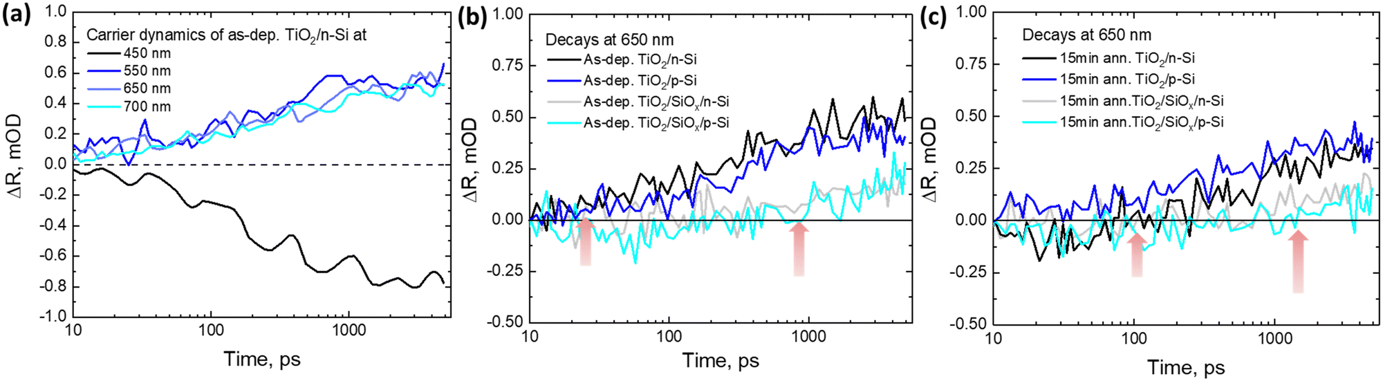 | ||
| Fig. 5 (a) Extracted charge transfer dynamics after excitation of the HF-treated as-dep. TiO2/n-Si sample at 500 nm (with 200 μJ cm−2 energy density) where the increase of the signal at different wavelengths is shown as a function of time which corresponds to the charge transfer signal increase at different wavelengths, and comparison of the extracted charge transfer signal increase at 650 nm probe wavelength for all the (b) HF-treated as-dep. TiO2/Si samples, and (c) 15 minute annealed TiO2/Si samples. The red arrow shows the charge transfer onset time where the charge transfer signal from Si to TiO2 first appears above the noise range. | ||
To compare the CT dynamics of all the TiO2/Si samples, the CT signal increase is compared at 650 nm probe wavelength as presented in Fig. 5b and c. The results show that the HF-treatment reduces the CT time from Si to TiO2 for both as-dep. TiO2/n-Si and as-dep. TiO2/p-Si samples and that the observed characteristic CT time (average time from where the CT signal increases from zero OD to the maximum OD on the 6 ns time scale of the TR measurement) is approx. 200 ps. However, for the as-dep. TiO2/SiOx/Si samples, the ones with chemical SiOx at the interface, the CT time prolongs ten fold, i.e., almost >2 ns, as shown in Fig. 5b. Previously, we reported a somewhat faster CT time of 600 ps in as-dep. TiO2/SiOx/Si samples while a similar fast CT time of 200 ps was observed for a HF-treated TiO2/Si samples.33 The results also agree with the surface barrier height results as there is a larger barrier for electrons when there is a SiOx layer. The photodynamics results also show that the CT signal does not keep increasing and saturates after approx. 1 ns. This occurs because charges accumulate near the TiO2 side of the interface due to the low carrier mobility in TiO2, taking approximately 1 μs to reach the surface,33 shown in Fig. 6.
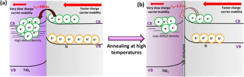 | ||
| Fig. 6 Schematic of photoinduced interfacial charge transfer in (a) as-dep. TiO2/n-Si and (b) 15 min annealed TiO2/n-Si samples. | ||
Hence, eventually, the CT process from Si to TiO2 is inhibited. In practical devices, this problem is typically addressed by making TiO2 thin enough (a few nm only) so that the carriers can reach the front surface despite the low mobility. As mentioned earlier, the samples were also annealed at 250 °C and 300 °C to investigate their thermal stability and its impact on the surface passivation. It can be observed that when the TiO2 films grown on both HF-treated p- and n-Si are annealed for 15 minutes at 250 °C, the characteristic CT time prolongs to almost 1.5 ns, as shown in Fig. 5c. The annealing induces the formation of interfacial SiOx that was previously shown to increase the CT time to 370 ps with low-defect anatase TiO2 coating.33 The prolonged CT time here can be rationalized by the differences between amorphous and crystalline TiO2. While in crystalline low-defect TiO2 electrons transfer to the conduction band, in amorphous TiO2 electrons can transfer to the impurity mediated defect states that are strongly modified by the annealing, shown in Fig. 6.
This prolonged CT time in annealed samples is therefore suggested to originate from the introduction of thermally originated interfacial SiOx at the TiO2–Si interface which hinders the CT process, and also from a reduction in the amount of available defect states within annealed TiO2 as compared to the as-deposited amorphous TiO2.33
The increase in the CT time could be linked to the decreasing tunneling probability with increasing SiOx barrier width. However, our optical instruments are not accurate enough to provide an estimate of the barrier thickness with sufficient accuracy for calculating the tunneling probability, which depends exponentially on the barrier thickness. The CT dynamics were also examined for HF-treated TiO2/n-Si samples annealed at 300 °C for even longer durations, i.e., for 60 and 90 minutes, to see the effect of higher temperature thermal treatment on the CT time. The results are shown in Fig. S6b in the ESI,† where it can be seen that the CT time prolongs even more, i.e., >5 ns.
Hence, it can be inferred that the samples exhibit limited thermal stability, consequently impacting the CT time and potentially impeding the efficiency of solar-to-electric conversion in Si-based PV devices. The characteristic CT times for all the HF-treated and untreated TiO2/n-Si heterojunctions (both as-dep. and annealed at 250 °C for different durations) are summarized in Table 1 and the results for TiO2/p-Si heterojunctions are presented in Table S3 in the ESI.† The results show that the CT times are strongly affected by the Si substrate pre-treatments, i.e., the Si surface, and sample post-treatments, i.e., a “thermally generated  layer at the TiO2–Si interface. However, the effect of doping on the CT time cannot be observed clearly in the case of our study as signals are weak and the differences are in the noise range.
| TiO2/n-Si (HF-treated series) | Characteristic CT time | TiO2/SiOx/n-Si (RCA2-treated series) | Characteristic CT time |
|---|---|---|---|
| As-deposited | 200 ps | As-deposited | 2.5 ns |
| 5 min annealed | 450 ps | 5 min annealed | 4 ns |
| 10 min annealed | 1 ns | 10 min annealed | >5 ns |
| 15 min annealed | 1.5 ns | 15 min annealed | >5 ns |
3.3. Impact of the annealing on TiO2
To investigate possible annealing induced morphological changes in TiO2 thin films, AFM images of TiO2/n-Si samples subjected to various annealing conditions were taken and the results for all the samples are shown in ESI,† Fig. S9. The results indicate that when the annealing is done at 250 °C for 5 to 15 minutes, the surface roughness increases only <0.1 nm compared to the as-deposited surface. Annealing at 300 °C increases the surface roughness a bit more but the topography remains to depict amorphous characteristics as shown in Fig. 7a and b, thus indicating some degree of structural changes in the TiO2 films presumably due to the desorption of impurity atoms introduced due to precursors during deposition. | ||
| Fig. 7 AFM images of (a) as-dep. TiO2/n-Si, (b) 90 min annealed TiO2/n-Si at 300 °C, (c) correlation of surface recombination velocity and surface roughness of the samples, and (d) correlation of surface recombination velocity and characteristic charge transfer times for HF-treated TiO2/n-Si heterojunctions annealed at 250 °C up to 15 minutes. | ||
Moreover, we observe a correlation between the surface roughness and the Seff values as shown in Fig. 7c where it can be seen that the Seff increase is the most significant during the initial annealing, i.e., when the as-dep. samples are thermally treated even for 5 minutes and after that it increases gradually for all annealed samples. It has been pointed out that the presence of H and Cl atoms in the as-deposited samples is favorable for surface passivation.29 In our study, Cl originates from the TiCl4 precursor during the ALD growth at low temperature while H originates from both the H2O precursor during ALD growth and HF dip prior to the ALD treatment. Also, the chemical SiOx contains hydrogen in the form of hydroxyl groups. However, upon the annealing, the H and Cl atoms can desorb from the samples which decreases the passivation quality of all the annealed TiO2 p- and n-Si samples.12
Furthermore, to observe the effect of thermal annealing on the charge carrier dynamics in TiO2 films solely, the samples were excited at 320 nm by TR spectroscopy to selectively photoexcite the carriers in TiO2.51 The photodynamics of the HF-treated TiO2/n-Si sample series is compared at 600 nm probe wavelength (Fig. S8, ESI†) and it can be seen that the lifetime of photocarriers in TiO2 does not improve when the samples are annealed for 5 to 15 minutes at 250 °C. However, annealing of the samples at 300 °C for 60 and 90 minutes slightly enhances the lifetime of the photogenerated carriers to ∼0.1 ns, but this is still less than the carrier lifetimes in crystalline TiO2 (∼4 ns, ref. 51).
Nevertheless, this enhancement in the lifetimes of photocarriers in annealed TiO2 films is rather minor and might be attributed to the slight reduction in the recombination centers (less defects and intra-band gap states, Fig. 6b) in them as compared to the as-dep. TiO2 films.51 This also suggests a slight reduction in the impurity related defects within TiO2 while maintaining their amorphous character as shown by the AFM images. To summarize, thermal annealing was found to improve the lifetimes of charge carriers generated within TiO2 films but were detrimental to the lifetime of carriers photogenerated within Si. The effect should be even more pronounced for the annealed samples that induce crystallization of TiO2 films.
3.4. Correlation of the surface passivation with the CT time through the TiO2/Si interface
All the as-dep. TiO2 films grown on HF-treated n-Si substrates show the minimum CT time of 200 ps as shown in Fig. 6. TiO2 is commonly used as an electron transport layer in various optoelectronic devices which means that it should keep accepting electrons from Si. However, our measurements show that the CT signal does not keep increasing and saturates after approx. 1 ns as shown in Fig. 5b and c. This happens as the transferred electrons fill up all the available energy states in the CB of the TiO2 and instead of moving to the TiO2 surface, the charges start accumulating at the TiO2 side of the interface because of the low carrier mobility in TiO2.33 This leads to inhibition of further acceptance of electrons in TiO2 from Si and thus, the CT stops. This contributes to the field effect passivation in TiO2–Si interfaces and the best passivation quality was obtained for samples showing the highest carrier saturation level. Although the Kelvin-probe found similar band bending regardless of the annealing time for TiO2/n-Si samples, these measurements are carried out under intense illumination and may saturate the TiO2 layer even with a slow CT process. Also, the as-dep. samples are rich in H and Cl impurities which further improves the chemical surface passivation at the TiO2–Si interface. However, it should be noted that the CT dynamics is sensitive to even subtle differences at the TiO2–Si interface and within TiO2, and a direct correlation is observed between the SRV and the CT process as a result of annealing, as shown in Fig. 7d. For instance, annealing the HF-treated samples at 250 °C even for 15 minutes introduces interfacial SiOx and induces desorption of the precursor traces and impurities from the amorphous TiO2 coating which in turn prolongs the CT time to 1.5 ns. Since passivation decreases and the CT time gets prolonged, these annealed samples are not suitable for achieving efficient performance in solar-to-energy conversion devices.4. Conclusions
This study investigates TiO2/Si heterojunctions, exploring the impact of pre-ALD chemical and post-ALD thermal treatments on interfacial SiOx layer formation, the TiO2 film composition, and the structure. This study examines surface passivation through effective carrier lifetime measurements and investigates CT dynamics using ultrafast transient reflectance spectroscopy. Photocarriers are selectively generated in Si at 500 nm excitation to analyze CT across the TiO2–Si interface. Findings reveal that HF-treated SiOx-free n-Si with as-deposited TiO2 exhibits the highest effective lifetime of 1.23 ms due to the bifunctional passivation of the surface combining both chemical and field effect passivation mainly caused by the precursors especially H impurities. Also, this sample exhibits the fastest CT time from Si to TiO2, within 200 ps, which is mainly due to the absence of interfacial SiOx which causes hindrance in the CT. Moreover, annealing increases the surface recombination velocity, possibly due to structural changes and precursor impurity desorption. The presence of the SiOx layer, whether chemically or thermally induced, increases the CT time and decreases the number of transferred carriers, adversely affecting the device performance. This research suggests potential for developing TMO-based passivating layers with improved charge transport properties and provides a framework applicable to other semiconductor surfaces and interfaces for understanding time-resolved photoinduced changes and photodynamics.5. Materials and methods
5.1. Scanning electron microscopy
For the thickness estimation of TiO2 thin films deposited by ALD, cross-sectional SEM images of the samples were taken by using a FEG Zeiss Gemini 500 SEM microscope in secondary and back scattered electron modes with an accelerating voltage of 3 kV and a working distance of 5 mm.5.2. AFM
To assess the topography of TiO2 thin films, atomic force microscopy images of the samples were taken by using AFM Bruker Icon in tapping mode.5.3. Steady state reflectance spectroscopy
The steady state reflectance spectra of the TiO2/Si samples were measured using a Shimadzu UV-3600 UV-Vis-NIR spectrophotometer. The measurements were carried out in the reflectance mode using a ‘Specular Reflectance Attachment for 5° Incidence Angle’ accessory with the spectrophotometer setup. Aluminium coated mirrors were used as reference mirrors. The spectra were recorded from 300 to 1200 nm.5.4. The injection-dependent effective lifetime τeff
The injection dependent effective lifetime was measured from the quarters by the contactless quasi steady-state photoconductance (QSSPC) method by using Sinton WCT-120 at room temperature. The software version for measurement and analysis is v5.72.0.10. For high lifetime (>100 μs) samples short-flash and transient analysis modes are used, while for low lifetime (<100 μs) samples long flash and generalized analysis modes are used. The reported lifetime was under an injection level of 1 × 1015 cm−3.5.5. Surface barrier height
The surface barrier height was determined using a Semilab PV-2000A to execute the Kelvin-probe method. Measurements of the contact potential difference between the wafer and a reference electrode were conducted under intense illumination (VlightCPD) and in complete darkness (VdarkCPD), and the surface barrier height (Vsb = VdarkCPD − VlightCPD) was determined based on the difference between the two lighting conditions. It was averaged from an area of 20 × 20 cm2 with a measurement step of 5 mm.5.6. Transient reflectance spectroscopy
Ultra-fast time-resolved pump–probe spectroscopy was used in reflectance mode to determine the optical properties of the TiO2/Si samples. The fundamental laser pulses were generated via a Ti:Sapphire laser (Libra F, Coherent Inc., 800 nm, approx. 100 fs pulse width, repetition rate 1 kHz). 90% of the fundamental beam was directed onto an optical parametric amplifier (Topas C, Light conversion Ltd) to produce the desired excitation wavelength (320 nm and 500 nm in our case), approximately 1 mm beam diameter at the sample, attenuated up to 200 μJ cm−2. 10% of the fundamental laser was delivered to the motorized stage (delay line) and then to a 2 mm cuvette with water to generate continuum white light for probe pulses. The probe light was split into the reference and signal beams. The absorbance change was measured in chopper mode which is synchronized with fundamental laser pulses. The samples were excited at 320 nm and 500 nm to selectively excite TiO2 and Si, respectively.33 The spectra were averaged over 3000 pulses for each delay time.Conflicts of interest
There are no conflicts to declare.Acknowledgements
The authors acknowledge the financial support of the Research Council of Finland (formerly Academy of Finland) via the Flagship on Photonics Research and Innovation ‘‘PREIN’’ #346511 (Tampere University) and #346529 (Aalto University). R. K. thanks Kaute foundation and Tampere University doctoral school for the funding. X. L. acknowledges the financial fundings from Business Finland (#7479/31/2019) and Research Council of Finland (#354199). V. V. acknowledges the financial funding from Research Council of Finland (#331313). Part of the research was performed at the OtaNano – Micronova Nanofabrication Centre of Aalto University.Notes and references
- S. Knez, S. Štrbac and I. Podbregar, Energy Sustainability Soc., 2022, 12, 1 CrossRef.
- S. Tagliapietra, G. Zachmann, O. Edenhofer, J.-M. Glachant, P. Linares and A. Loeschel, Energy Policy, 2019, 132, 950–954 CrossRef.
- S. Park, J. Ha, M. F. Khan, C. Im, J. Y. Park, S. H. Yoo, M. A. Rehman, K. Kang, S. H. Lee and S. C. Jun, ACS Appl. Electron. Mater., 2022, 4, 4306–4315 CrossRef CAS.
- N. Asim, K. Sopian, S. Ahmadi, K. Saeedfar, M. A. Alghoul, O. Saadatian and S. H. Zaidi, Renewable Sustainable Energy Rev., 2012, 16, 5834–5847 CrossRef CAS.
- T. G. Allen, J. Bullock, X. Yang, A. Javey and S. De Wolf, Nat. Energy, 2019, 4, 914–928 CrossRef CAS.
- R. Fan, Z. Mi and M. Shen, Opt. Express, 2019, 27, A51–A80 CrossRef CAS.
- F. Decker and S. Cattarin, in Encyclopedia of Electrochemical Power Sources, ed. J. Garche, Elsevier, Amsterdam, 2009, pp. 1–9 Search PubMed.
- R. S. Bonilla and P. R. Wilshaw, Appl. Phys. Lett., 2014, 104, 232903 CrossRef.
- A. Tyagi, K. Ghosh, A. Kottantharayil and S. Lodha, IEEE Trans. Electron Devices, 2019, 66, 1377–1385 CAS.
- H. Lin, M. Yang, X. Ru, G. Wang, S. Yin, F. Peng, C. Hong, M. Qu, J. Lu, L. Fang, C. Han, P. Procel, O. Isabella, P. Gao, Z. Li and X. Xu, Nat. Energy, 2023, 8, 789–799 CrossRef CAS.
- M. A. Rehman, S. Park, M. F. Khan, M. F. Bhopal, G. Nazir, M. Kim, A. Farooq, J. Ha, S. Rehman, S. C. Jun and H.-H. Park, Int. J. Energy Res., 2022, 46, 11510–11522 CrossRef CAS.
- M. M. Shehata, G. Bartholazzi, D. H. Macdonald and L. E. Black, Adv. Energy Mater., 2023, 13, 2300251 CrossRef CAS.
- B. S. Richards, J. E. Cotter, C. B. Honsberg and S. R. Wenham, Conference Record of the Twenty-Eighth IEEE Photovoltaic Specialists Conference, 2000, pp. 375–378.
- G. S. Sahoo, C. Harini, N. Mahadevi, P. S. Nethra, A. Tripathy, M. Verma and G. P. Mishra, Silicon, 2023, 15, 4039–4048 CrossRef CAS.
- A. Rehman, M. F. Khan, M. A. Shehzad, S. Hussain, M. F. Bhopal, S. H. Lee, J. Eom, Y. Seo, J. Jung and S. H. Lee, ACS Appl. Mater. Interfaces, 2016, 8, 29383–29390 CrossRef CAS PubMed.
- A. Richter, S. W. Glunz, F. Werner, J. Schmidt and A. Cuevas, Phys. Rev. B: Condens. Matter Mater. Phys., 2012, 86, 165202 CrossRef.
- L. G. Gerling, C. Voz, R. Alcubilla and J. Puigdollers, J. Mater. Res., 2017, 32, 260–268 CrossRef CAS.
- B. W. H. van de Loo, B. Macco, J. Melskens, W. Beyer and W. M. M. Kessels, J. Appl. Phys., 2019, 125, 105305 CrossRef.
- S. Acharyya, S. Sadhukhan, T. Panda, D. K. Ghosh, N. C. Mandal, A. Nandi, S. Bose, G. Das, S. Maity, P. Chaudhuri, H. Saha and D. Banerjee, Surf. Interfaces, 2022, 28, 101687 CrossRef CAS.
- T. Mochizuki, K. Gotoh, A. Ohta, S. Ogura, Y. Kurokawa, S. Miyazaki, K. Fukutani and N. Usami, Appl. Phys. Express, 2018, 11, 102301 CrossRef.
- K. M. Gad, D. Vössing, A. Richter, B. Rayner, L. M. Reindl, S. E. Mohney and M. Kasemann, IEEE J. Photovolt., 2016, 6, 649–653 Search PubMed.
- B. Liao, B. Hoex, A. G. Aberle, D. Chi and C. S. Bhatia, Appl. Phys. Lett., 2014, 104, 253903 CrossRef.
- Z.-P. Yang, H.-E. Cheng, I.-H. Chang and I.-S. Yu, Appl. Sci., 2016, 6, 233 CrossRef.
- J. Cui, T. Allen, Y. Wan, J. Mckeon, C. Samundsett, D. Yan, X. Zhang, Y. Cui, Y. Chen, P. Verlinden and A. Cuevas, Sol. Energy Mater. Sol. Cells, 2016, 158, 115–121 CrossRef CAS.
- G. S. Park, S. Lee, D.-S. Kim, S. Y. Park, J. H. Koh, D. H. Won, P. Lee, Y. R. Do and B. K. Min, Adv. Energy Mater., 2023, 13, 2203183 CrossRef CAS.
- T.-C. Chen, T.-C. Yang, H.-E. Cheng, I.-S. Yu and Z.-P. Yang, Appl. Surf. Sci., 2018, 451, 121–127 CrossRef CAS.
- K. Gotoh, T. Mochizuki, T. Hojo, Y. Shibayama, Y. Kurokawa, E. Akiyama and N. Usami, Curr. Appl. Phys., 2021, 21, 36–42 CrossRef.
- M. M. Plakhotnyuk, N. Schüler, E. Shkodin, R. A. Vijayan, S. Masilamani, M. Varadharajaperumal, A. Crovetto and O. Hansen, Jpn. J. Appl. Phys., 2017, 56, 08MA11 CrossRef.
- B. Liao, N. Dwivedi, Q. Wang, R. J. Yeo, A. G. Aberle, C. S. Bhatia and A. Danner, IEEE J. Photovolt., 2021, 11, 319–328 Search PubMed.
- Y. Chang, J. R. Yates and C. E. Patrick, ACS Omega, 2023, 8, 20138–20147 CrossRef CAS PubMed.
- H. Liu, J. Tang, I. J. Kramer, R. Debnath, G. I. Koleilat, X. Wang, A. Fisher, R. Li, L. Brzozowski, L. Levina and E. H. Sargent, Adv. Mater., 2011, 23, 3832–3837 CrossRef CAS.
- H. Hu, B. Dong, H. Hu, F. Chen, M. Kong, Q. Zhang, T. Luo, L. Zhao, Z. Guo, J. Li, Z. Xu, S. Wang, D. Eder and L. Wan, ACS Appl. Mater. Interfaces, 2016, 8, 17999–18007 CrossRef CAS PubMed.
- R. Khan, H. P. Pasanen, H. Ali-Löytty, H. M. Ayedh, J. Saari, V. Vähänissi, M. Valden, H. Savin and N. V. Tkachenko, Surf. Interfaces, 2023, 38, 102871 CrossRef CAS.
- J. Ott, T. P. Pasanen, P. Repo, H. Seppänen, V. Vähänissi and H. Savin, Phys. Status Solidi A, 2019, 216, 1900309 CrossRef.
- C. Luderer, D. Kurt, A. Moldovan, M. Hermle and M. Bivour, Sol. Energy Mater. Sol. Cells, 2022, 238, 111412 CrossRef CAS.
- H. P. Pasanen, P. Vivo, L. Canil, H. Hempel, T. Unold, A. Abate and N. V. Tkachenko, J. Phys. Chem. Lett., 2020, 11, 445–450 CrossRef CAS PubMed.
- R. Khan, H. Ali-Löytty, J. Saari, M. Valden, A. Tukiainen, K. Lahtonen and N. V. Tkachenko, Nanomaterials, 2020, 10, 1567 CrossRef CAS PubMed.
- H. P. Pasanen, R. Khan, J. A. Odutola and N. V. Tkachenko, J. Phys. Chem. C, 2024, 128, 6167–6179 CrossRef CAS PubMed.
- N. V. Tkachenko and R. Khan, in Tailored Functional Oxide Nanomaterials, eds. C. Maccato and D. Barreca, Wiley, 1st edn, 2022, pp. 193–228 Search PubMed.
- O. M. E. Ylivaara, A. Langner, X. Liu, D. Schneider, J. Julin, K. Arstila, S. Sintonen, S. Ali, H. Lipsanen, T. Sajavaara, S.-P. Hannula and R. L. Puurunen, Thin Solid Films, 2021, 732, 138758 CrossRef CAS.
- N. E. Grant, V. P. Markevich, J. Mullins, A. R. Peaker, F. Rougieux, D. Macdonald and J. D. Murphy, Phys. Status Solidi A, 2016, 213, 2844–2849 CrossRef CAS.
- W. Kern, Handbook of Silicon Wafer Cleaning Technology, 3rd edn, 2018, p. 978-0-323-51084-4 Search PubMed.
- D. Rouchon, N. Rochat, F. Gustavo, A. Chabli, O. Renault and P. Besson, Surf. Interface Anal., 2002, 34, 445–450 CrossRef CAS.
- J. Saari, H. Ali-Löytty, M. Honkanen, A. Tukiainen, K. Lahtonen and M. Valden, ACS Omega, 2021, 6, 27501–27509 CrossRef CAS PubMed.
- R. Methaapanon and S. F. Bent, J. Phys. Chem. C, 2010, 114, 10498–10504 CrossRef CAS.
- H. Liu, T. P. Pasanen, O. Leiviskä, J. Isometsä, T. H. Fung, M. Yli-Koski, M. Miettinen, P. Laukkanen, V. Vähänissi and H. Savin, Appl. Phys. Lett., 2023, 122, 191602 CrossRef CAS.
- N. E. Grant, A. I. Pointon, R. Jefferies, D. Hiller, Y. Han, R. Beanland, M. Walker and J. D. Murphy, Nanoscale, 2020, 12, 17332–17341 RSC.
- X. Liu, B. Radfar, K. Chen, E. Pälikkö, T. P. Pasanen, V. Vähänissi and H. Savin, IEEE Photonics Technol. Lett., 2022, 34, 870–873 CAS.
- X. Liu, B. Radfar, K. Chen, T. P. Pasanen, V. Vähänissi and H. Savin, Adv. Photonics Res., 2022, 3, 2100234 CrossRef CAS.
- A. G. Scheuermann, C. E. D. Chidsey and P. C. McIntyre, J. Electrochem. Soc., 2015, 163, H192 CrossRef.
- R. Khan, H. Ali-Löytty, A. Tukiainen and N. V. Tkachenko, Phys. Chem. Chem. Phys., 2021, 23, 17672–17682 RSC.
Footnotes |
| † Electronic supplementary information (ESI) available. See DOI: https://doi.org/10.1039/d4cp00992d |
| ‡ Both of the authors contributed equally to this article. |
| This journal is © the Owner Societies 2024 |