
 Open Access Article
 This Open Access Article is licensed under a
 Creative Commons Attribution 3.0 Unported Licence
Colloidal 2D Mo1−xWxS2 nanosheets: an atomic- to ensemble-level spectroscopic study†
Markus
Fröhlich
 a,
Marco
Kögel
b,
Jonas
Hiller
a,
Leo
Kahlmeyer
a,
Alfred J.
Meixner
a,
Marcus
Scheele
a,
Jannik C.
Meyer
bc and
Jannika
Lauth
*ad
a,
Marco
Kögel
b,
Jonas
Hiller
a,
Leo
Kahlmeyer
a,
Alfred J.
Meixner
a,
Marcus
Scheele
a,
Jannik C.
Meyer
bc and
Jannika
Lauth
*ad
aUniversity of Tübingen, Institute of Physical and Theoretical Chemistry, Auf der Morgenstelle 18, D-72076, Tübingen, Germany. E-mail: jannika.lauth@uni-tuebingen.de
bNMI Natural and Medical Sciences Institute at the University of Tübingen, Markwiesenstraße 55, D-72770 Reutlingen, Germany
cUniversity of Tübingen, Institute of Applied Physics, Auf der Morgenstelle 10, D-72076 Tübingen, Germany
dLeibniz University of Hannover, Cluster of Excellence PhoenixD (Photonics, Optics and Engineering – Innovation Across Disciplines), Welfengarten 1a, D-30167, Hannover, Germany
First published on 1st April 2024
Abstract
Composition dependent tuning of electronic and optical properties in semiconducting two-dimensional (2D) transition metal dichalcogenide (TMDC) alloys is promising for tailoring the materials for optoelectronics. Here, we report a solution-based synthesis suitable to obtain predominantly monolayered 2D semiconducting Mo1−xWxS2 nanosheets (NSs) with controlled composition as substrate-free colloidal inks. Atomic-level structural analysis by high-angle annular dark-field (HAADF) scanning transmission electron microscopy (STEM) coupled with energy dispersive X-ray spectroscopy (EDXS) depicts the distribution of individual atoms within the Mo1−xWxS2 NSs and reveals the tendency for domain formation, especially at low molar tungsten fractions. These domains cause a broadening in the associated ensemble-level Raman spectra, confirming the extrapolation of the structural information from the microscopic scale to the properties of the entire sample. A characterization of the Mo1−xWxS2 NSs by steady-state optical spectroscopy shows that a band gap tuning in the range of 1.89–2.02 eV (614–655 nm) and a spin–orbit coupling-related exciton splitting of 0.16–0.38 eV can be achieved, which renders colloidal methods viable for upscaling low cost synthetic approaches toward application-taylored colloidal TMDCs.
Introduction
Two-dimensional (2D) transition metal dichalcogenides (TMDCs) have been extensively studied over the past decade owing to their rich exciton physics.1,2 This research period was sparked by the crossover from an indirect to a direct band gap in MoS2 when approaching monolayer (ML) thickness; first described by Mak et al. for mechanically exfoliated MoS2 MLs in 2010.3,4 A multitude of applications in light detection5,6 and light harvesting,7 catalysis,8 gas sensor technology9 and lately spin- and valleytronics10 have been established.The most prominent TMDC examples MoS2 and WS2 exhibit electronic transitions in the energy range of 1.9–3.5 eV (at UV-Vis wavelengths, 350–650 nm). Originating from strong spin–orbit coupling (SOC), the valence bands of MoS2 and WS2 are split, generating two spin states.11 Excitations from the lower energy state are referred to as the A excitonic transition, while the higher energy transition from the lower-lying spin state is called the B excitonic transition. At higher energies, C and D exciton transitions are observed. The C exciton in MoS2 originates from a nearly degenerate transition in a band nesting region.11 In contrast, for WS2, the C and D exciton stem from direct transitions.12–14 The vertical confinement in 2D TMDCs leads to a reduced dielectric screening compared to the solid-state material and causes strong exciton binding energies. Besides the considerable vertical confinement, the lateral dimension of binary TMDC nanosheets (NSs) (e.g. MoS2, WS2), can be used to finetune exciton energies. For example, in colloidal 2D MoS2 NSs, a hypsochromic shift of 70 meV (from 590–611 nm) has been realized by reducing the lateral size of the structures from 22 to 7 nm.15
Additionally to thickness and lateral size variation, tailoring of the elemental composition of ternary TMDCs (e.g. Mo1−xWxS2) enables tuning of the band gap, electronic structure and hence the optical properties of the materials.16 This includes band gap shifts bridging the entire energy range between pure MoS2 (1.88 eV)17 and pure WS2 (2.01 eV).18,19 Strong SOC originating from transition metal d-orbitals is inherent in 2D TMDCs.16 The splitting between the A and B exciton in Mo1−xWxS2 correlates with the mole fraction x of the heavier tungsten atom and ranges from 0.140 eV for MoS2 to 0.4 eV in WS2.20
To use the optical and photophysical properties of 2D colloidal semiconducting nanomaterials to their full potential, controlling their thickness and lateral size, as well as the associated band structure is thus of major importance. While the exfoliation of solid-state materials and vapour phase syntheses are well studied, wet-chemical syntheses of TMDCs are comparatively unexplored. Colloidal chemistry allows for the control of the lateral size, thickness, crystal phase, elemental composition and yields considerable amounts of close to monodisperse product.21 In 2014 Mahler et al. adapted a colloidal protocol to produce TMDCs via wet chemistry.22 Expanding on this, Sun et al. published the colloidal synthesis of MoxW1−xSe2, WS2ySe2(1−y)23 and MoxW1−xTe224 in 2017. Recently Pippia et al. demonstrated the synthesis of fluorescent MoS2 and MoSe2 NSs,25 while our group developed a protocol for the synthesis of fluorescent WS2,26 followed by a selective wet-chemical route to phase-pure 2H-MoS2 NSs and laterally confined MoS2 nanoplatelets15
Here, we report the wet-chemical synthesis of colloidal Mo1−xWxS2 NS alloys with controlled Mo/W ratios. Size, structure and distribution of molybdenum and tungsten at the atomic scale are investigated by HAADF-STEM imaging. We obtain NSs of mono- to few-layer thickness with a lateral size of 5–20 nm. Spatially resolved EDXS shows a homogeneous distribution of the employed Mo/W ratios. Additionally, Raman spectroscopy confirms these findings and the synthesis of the pure semiconducting 2H phase on a macroscopic level. Composition-dependent shifts in vibrational frequencies of the E′ and  modes are in excellent agreement with previous reports.27 Furthermore, we report on a linear correlated A–B exciton splitting due to increased SOC in WS2-rich alloys and band gap tuning in the range of 1.89–2.02 eV (614–655 nm). Tuning the SOC is vital for the implementation of 2D TMDCs in spin- and valley-tronics and make colloidal 2D TMDC alloys promising candidates for future applications.28
Experimental
Materials
1,2-Dichlorobenzene (O-DCB, 99%), ethanol (99,8%), n-hexane (97%), oleylamine (OlAm, 98%) and sulphur (99.98%) were purchased from Sigma Aldrich. Molybdenum(V) chloride (99%) and tungsten(VI) chloride (99%) were purchased from Alfa Aesar and 1,1,1,3,3,3-hexamethyldisilazane (HMDS, 98%) was purchased from Acros Organics.OlAm was degassed under vacuum at 120 °C for 6 h before being stored under inert gas atmosphere inside a nitrogen filled glovebox alongside with MoCl5, WCl6, sulphur and HMDS. All chemicals were used as supplied without further purification.
Synthesis of Mo1−xWxS2 alloyed nanosheets
The synthesis was adapted from Niebur and Söll et al.15 and was optimized to suit the formation of mono- to few-layered 2H-phase colloidal Mo1−xWxS2 NSs stable in o-DCB. Changes to the reaction protocol contained the reduction of the overall concentration of the metal- and sulphur-precursor, sulphur excess and the reduction of the addition rate.Inside a nitrogen filled glovebox, the Mo-precursor and W-precursor stock solutions were prepared by dissolving MoCl5 and WCl6 (37 μmol, 10 mg and 37 μmol, 14.5 mg, resp., see Table S1, ESI†) in 20 mL OlAm. Sulphur (249 μmol, 8 mg) was dissolved in 17.5 mL OlAm and 2.5 mL HMDS to obtain the S-precursor solution.
For all Mo1−xWxS2 NS syntheses, a three-neck-flask was filled with 15 mL OlAm and 5 mL of the S-precursor solution. Immediately before the reaction, 10 mL of the respective metal-precursor mixture (Mo/W: 1/0, 0.75/0.25, 0.5/0.5, 0.25/0.75, 0/1) was prepared in a syringe.
On a Schlenk line, the sulphur solution was heated to 320 °C under inert gas atmosphere. Upon reaching the reaction temperature, the metal-precursor mixture was added dropwise via a syringe pump (10 mL h−1). The reaction mixture was allowed to cool down to room temperature after 30 minutes, exposed to air and precipitated with 60 mL of ethanol. The crude reaction product was washed with 20 mL of n-hexane and redispersed in o-DCB to yield the NS ink, which was stored under ambient conditions until use.
Scanning transmission electron microscopy
STEM images were obtained using a JEOL ARM 200F equipped with a CESCOR aberration corrector operating at 80 kV. Samples for STEM analysis were prepared by drop-casting the colloidal Mo1−xWxS2 NS solution onto graphene-coated MEMS (Graphenea easy-transfer) heating chips obtained from Hennyz.com Solutions. The dry sample was washed with n-hexane and ethanol and annealed at 150 °C overnight under high vacuum of the electron microscope to remove mobile carbon contaminations.Raman spectroscopy
Raman spectra were recorded using a home-built inverted confocal laser stage scanning microscope. A 532 nm Coherent COMPASS 215M-75 SL Laser was employed as the excitation source. The signal was recorded by a ProEM+ 512B eXcelon camera attached to a Princeton Instruments Acton SP-2-500i spectrometer, using a 1200 g mm−1 grating. Prior to the measurements, the instrument was calibrated using a Neon gas-discharge lamp. The temperature of the camera was set to −70 °C. The Raman spectra were acquired under ambient conditions by focusing the excitation laser through an infinity corrected 60×/0.80 air objective to a diffraction limited focal area on a drop-casted film of the material and recording the non-elastic scattering. The laser line was removed by two RazorEdge Long Pass E-Grade 532 filters, excluding all signals below 100 cm−1.UV-Vis absorbance spectroscopy
UV-Vis absorbance spectra were acquired on an Agilent Cary 5000, using a quartz cuvette (quartz glass high performance QS 200–2500 nm by Hellma) with a path length of 1 cm (optical density below 0.2 at 350 nm) All samples were dispersed in o-DCB for maximum colloidal stability.29Results and discussion
Structure and size of Mo1−xWxS2 alloyed nanosheets
Due to closely matching lattice parameters, MoS2 and WS2 ternary alloys can be obtained in any ratio.30 The structural identification in terms of composition and alloying degree on the other hand remains challenging since a small lattice mismatch of 0.2%31 in the materials in combination with naturally occurring folding, stacking and agglomeration of 2H phase MoS215 and WS222 NSs in colloidal solution, leads to broadening and rather poor reflex separation in X-ray diffractograms.23 Here, we opted for HAADF-STEM imaging coupled with EDXS for structural information about the colloidal Mo1−xWxS2 alloyed NSs to solve this problem.
Fig. 1a shows a HAADF image of a flat-on oriented ML of Mo0.5W0.5S2. The NSs of 5–25 nm lateral size distributed around an average of 13 nm (see Fig. S1, ESI†) are readily, but not exclusively, found at the edges of bigger agglomerates referred to as nanoflowers.15 When zooming in from low magnification, the nanoflowers act as a guide to find MLs as has been previously reported.15,23,24 Moving away from the nanoflowers, a thin surface coverage of the graphene substrate with MLs of 2D TMDCs is observed (see Fig. S2, ESI†). We assume that van der Waals forces between graphene and the NSs in combination with long annealing times (150 °C, overnight) allow the NSs to align with the graphene surface. The FFT inset in Fig. 1a shows the first and second order diffraction peaks of the crystal lattice around the (001) plane axis. The hexagonal pattern is evident for a single crystalline 2H-phase configuration of the depicted Mo0.5W0.5S2 ML.32 The Z-contrast-mapping of the HAADF STEM image (Fig. 1a) was translated to a colormap, ranging from purple (Mo) to orange (W) to counteract the surrounding dependent grey perception of the human eye.33 The S atoms’ contrast is comparatively low and blends in the background. Fig. 1b shows a line cut along the [10![[1 with combining macron]](https://www.rsc.org/images/entities/char_0031_0304.gif) 0] direction (indicated by the white arrow in Fig. 1a) of the ML taken from Fig. 1a. Mo, W and S are sufficiently distinguishable by Z-contrast, with the W contrast being twice as strong as the one of Mo and S. Even though Mo and S are not divided as well by contrast as W and Mo, the metal and chalcogen positions are exclusive in the lattice, meaning that S and Mo are easily separated.
0] direction (indicated by the white arrow in Fig. 1a) of the ML taken from Fig. 1a. Mo, W and S are sufficiently distinguishable by Z-contrast, with the W contrast being twice as strong as the one of Mo and S. Even though Mo and S are not divided as well by contrast as W and Mo, the metal and chalcogen positions are exclusive in the lattice, meaning that S and Mo are easily separated.
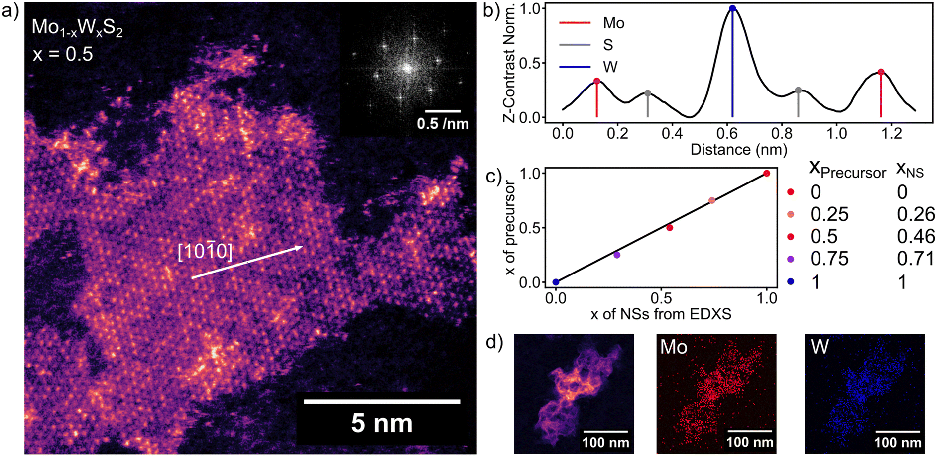 | ||
| Fig. 1 (a) HAADF-STEM image displaying a Mo1−xWxS2 NS of 50/50 composition and ML thickness. The Z-contrast is rendered as a colormap, with Mo in purple and W in orange. The FFT inset in the top-right corner shows the distinct features of the 2H semiconducting crystal phase. (b) Line profile along the [100] direction of the ML emphasizes the distinguishability of Mo and W by Z-contrast. (c) Summarized EDXS measurements comparing the precursor composition with the NS composition showing good accordance. (d) Left: HAADF-STEM image of a nanoflower consisting of an agglomerate of individual NSs, middle: EDXS maps of the same nanoflower, with coloured Mo-atoms in red and right: W-atoms in blue. | ||
Elemental composition
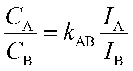
The elemental composition of colloidal Mo1−xWxS2 alloys determined by EDXS (Fig. 1d) is compared with the stoichiometry targeted by the precursor composition during the synthesis shown in Fig. 1c. The measurements show good agreement with the stoichiometry from synthesis as is indicated by a linear correlation (R2 = 0.9966) between precursor and NS composition. Fig. 1d shows a HAADF image (left) of an agglomerated nanoflower. EDXS of these clusters offers better signal to noise ratio than ML EDXS and is therefore used to determine the elemental composition of the samples. Elemental maps in Fig. 1d of Mo (middle) and W (right) were extracted by integrating EDXS peaks after background removal.For the quantification in Fig. 1c (xNs), hyperspectral images were summed up to a single spectrum. Fitted peak intensities of Mo-Kα (15.112 keV) and W-Lα (9.738 keV) were used for a Cliff–Lorimer quantification with k-factors determined using commercially obtained mechanically exfoliated samples. The Cliff–Lorimer method allows to calculate the concentration of two elements within a thin (10 nm or less) sample. Characteristic X-ray intensities IA and IB relate to the elemental compositions CA and CB as follows.34
Alloying degree
Besides the composition of Mo1−xWxS2, alloys are also described by their alloying degree. It helps to differentiate whether Mo and W share the same crystal lattice in homogenous distribution or if the NSs contain pure MoS2 and WS2 domains. While small inhomogeneities might not affect the ensemble properties, largely varying local environments may e.g. produce broadened features for vibrational or electronic transitions.35,36 The alloying degree is therefore a useful tool to quantify the dispersion of atoms in bimetallic alloys.37To determine the distribution and subsequently the alloying degree as well as eventual domain sizes, a digital model of the real lattice of the recorded HAADF-STEM images was generated. For this, areas of ML thickness with negligible or constant background were selected as shown in Fig. 2a (white outline). The metal sites of the crystal lattice were projected onto the HAADF-STEM image by inverse FFT of the lattice to eliminate the S atoms. The chalcogen sites have been omitted in our case as only sulfide alloys are investigated in this study. The resulting histogram (Fig. 2b) is fitted with two Gaussian functions, representing the population of Mo and W atoms. The intersection of the Gaussians was used as the cut off Z-contrast between Mo and W. Now every atom in the metal-lattice is identified as Mo or W atom and the coordination of each neighbouring atom with Mo or W atoms and vice versa is calculated. The measured distribution is compared with a theoretical random distribution of atoms in Fig. 2c and d. Looking at the distribution, the higher molar fraction W is following the simulation quite well. Mo however does gravitate towards higher Mo-coordination than expected by a random distribution. These qualitative findings will be quantified and summarized for all samples in the following section.
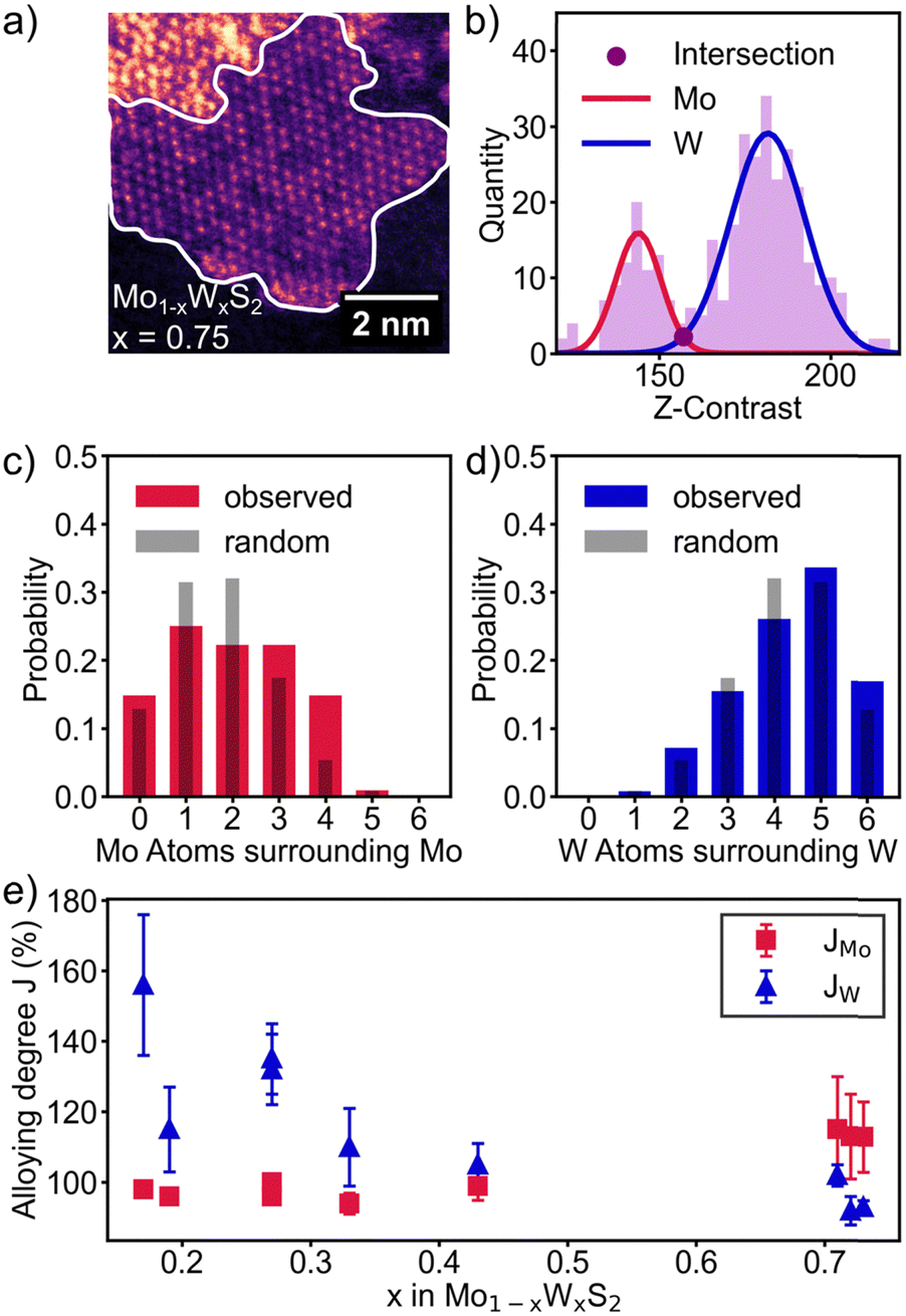 | ||
| Fig. 2 (a) HAADF-STEM image of a monolayered Mo1−xWxS2 NS (x = 0.75) with Mo island formation visible as dark patches. (b) Z-Contrast histogram of the image shown in (a) fitted with two Gaussian functions separating Mo (red) and W (blue). (c) and (d) Coordination of Mo atoms with Mo (red) and W atoms with W (blue) compared with a simulated random distribution (gray). (e) Alloying degree J as function of alloy composition, indicating homophily for both Mo and W at low concentrations. | ||
The alloying degree JMo for Mo can be defined as the fraction of the observed Mo atoms surrounding a Mo atom, divided by the expected value for a homogeneous alloy of the given composition.37JW can be calculated analogously.
| JMo = Pobserved/Pexpected × 100% |
Raman spectroscopy
To support results discussed above where the composition and distribution of Mo and W in colloidal Mo1−xWxS2 NS alloys are visualized on the atomic scale, Raman scattering spectroscopy offers structural information of the whole ensemble. Fig. 3a shows Raman spectra of the investigated colloidal samples. The WS2-like E′, MoS2-like E12g and the shared A1g modes are distinguishable, while distinct features of the 1T metallic phase (J1, J2, J3) between 150 and 350 cm−1 are absent in all samples.39 However, below 250 cm−1 acoustic phonon modes of the 2H semiconducting MoS2 and WS2 phase can be observed instead.40,41 Previous research linked the wavenumbers of the and E′ modes to the alloy composition and the broadening to reduced disorder.27 The A1g wavenumber correlates with x in Mo1−xWxS2 and shifts from 403 (MoS2) to 413 cm−1 (WS2, see Fig. 3b). The MoS2-like E12g signal is negatively correlated with x between 380 and 369 cm−1, while the WS2-like E′ mode (∼350 cm−1) seems to be less affected by the composition of the alloy. These general trends as well as the absolute position are in good accordance with previous studies.27 Remarkably, the x = 0.25 alloy is outlying in all of Fig. 3b with an upwards shifted wavenumber in relation to the trend.
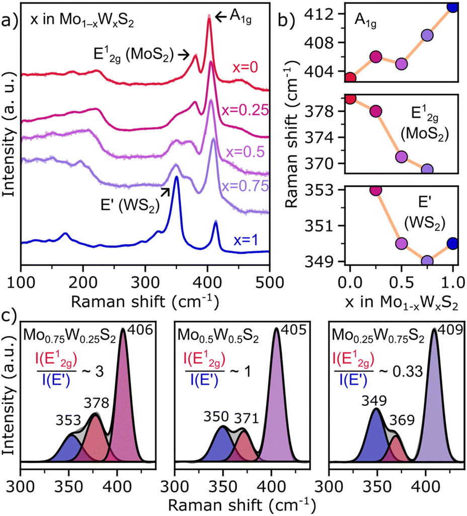 | ||
| Fig. 3 (a) Raman spectra of Mo1−xWxS2 NSs (x = 0–1) plotted with an offset and showing the gradual change from MoS2 to WS2. (b) Composition dependent Raman shifts of the (from top to bottom) A1g, MoS2-like E12g and WS2-like E′ vibrational modes. (c) Mo and W ratios calculated by integrating the intensity of the fitted A1g, E12g and E′ features of (from left to right) Mo1−xWxS2 (x = 0.25, 0.5, 0.75) aligning well with the EDXS measurements. | ||
In Fig. 3a, not only wavenumber shifts but also variations in intensity are observed. For instance, an unusually strong intensity of the signal at 350 cm−1 in pure WS2 NSs is found. This signal was found to be a combination of the WS2-like E′ feature that is also seen in the alloyed samples and a 2LA(M) acoustic mode.42 The 2LA(M) in WS2 originates from resonant excitation of the B exciton with the 532 nm Laser. Therefore, shifting of the B exciton by alloying reduces the contribution of the acoustic mode drastically, which is why the intensity of the signal at around 350 cm−1 immediately plunges when Mo is introduced to the lattice. Another factor that determines the intensity of the 2LA(M) mode is the layer number. For a ML, an intensity-ratio R = I(2LAM)/I(A1g) > 2 was found.42 For colloidal WS2 NSs shown here, this ratio R is approximately 2.5, and underpins the monolayer thickness of this sample.
Another way to quantify the alloy composition are the relative intensities of the MoS2-like E12g and the WS2-like E′ mode.27 In Fig. 3c, the Raman spectra of the alloys are background corrected and the individual modes of interest are fitted using a Gaussian function. The obtained intensity ratios are in good agreement with the EDXS measurements shown in Fig. 1c. It should be noted, however, that due to the overlapping of the E12g and E′ modes, the intensity ratio can be influenced by the specific background correction and fitting parameters, limiting this method to approximate values (see Fig. S3, ESI†).
When comparing the FWHM of the fitted peaks, again an outlier occurs for x = 0.25. The FWHM of the E′-mode in the left panel of Fig. 3c is broadened by ∼4 cm−1 compared to both other compositions. A possible explanation for this broadening could be an uneven distribution of Mo and W, as it was reported for other systems.35,43,44 Fitting to this explanation, we saw a significant homophilic behaviour among the W atoms in NSs with low W content as is discussed for Fig. 2d. Whether this phenomenon is also responsible for the deviation in shifts mentioned above will need further investigation.
Absorbance spectroscopy
UV-Vis absorbance spectroscopy was used to investigate the effect of alloying on the optical properties of Mo1−xWxS2 NSs. The raw data was acquired as described above and is shown in Fig. 4a (offset for better visibility). The spectra were then background corrected by subtracting the contribution of the wavelength dependent (nonlinear) Rayleigh scattering of the suspended NSs (see Fig. S4, ESI†). To better resolve convoluted features, the second derivative of the absorption is taken. This method is known to improve the spectral resolution and to eliminate contribution from linear backgrounds in exchange for an exaggerated noise.45 The spectra are first smoothed by a Savitzky–Golay filter before derivation. In Fig. 4b, the second derivative of the absorption spectra of all Mo1−xWxS2 samples in the range of 300 to 800 nm is shown with an offset for visibility. The excitonic transitions from low to high energy A, B, C and D are clearly separated with arrows indicating the trend for the shifting energies. By our alloying approach, it is possible to tune both, the position of the A (1.89–2.02 eV, 614–655 nm) and B exciton (2.05–2.40 eV, 517–605 nm), as well as the A–B splitting (0.15–0.38 eV) shown in Fig. 4b. These values are in good accordance with literature.20 Excitonic shifts of five series (Mo1−xWxS2, x = 0, 0.25, 0.5, 0.75, 1) of syntheses are averaged and summarized in Fig. 4c and d. The band edge transitions A and B originate both at the K point of the Brillouin zone and due to a major contribution of the transition metal d-orbitals’ SOC, the valence band is spin-split into the lower energy A and higher energy B transition.11 Between the Γ and Λ point in the Brillouin zone of MoS2, a band nesting region (C exciton) arises from parallelly running degenerate energy bands that are split in WS2 due to higher SOC and yield two discrete transitions.14 The C exciton energy seems to not correlate with the composition of the alloy, which supports the previous claim that the origins of the post band gap transitions in MoS2 (band nesting) and WS2 (hill-valley-transition) are different, leading to an inconsistent shift. The D exciton on the other hand is suspected to originate from a direct transition like A and B, but close to the Γ point.12 Here again, a rather linear correlation between the composition and the position of the excitonic transition is observed (Fig. 4d). All mole fractions in Fig. 4c and d show a deviation from a perfectly linear correlation but are consistent over all syntheses as is indicated by the error bars shown in Fig. 4c and d. DFT calculations by Tongay et al.46 explained this behavior for the A exciton by stating that the conduction band minimum (CBM) of the alloy at the K point mainly consists of lower lying dz2 orbitals of Mo even at low Mo-ratios, while the valence band maximum (VBM) is composed of uniformly distributed dxy and dx2−y2 orbitals.16 By incorporating Mo, the CBM therefore drops rapidly, while the VBM decreases linearly with the composition, which results in a bowing effect towards the W-rich composition of the alloy. Even though the B exciton originates from a lower valence band state, the nonlinearity of the CBM towards compositional changes effects the B exciton in the same way and results in a similar bowing effect. The D exciton is following the same trend and is also subject to bowing in the W-rich region, which suggests that the conduction band composition described above is true, not only at the K point but also for the rest of the Brillouin zone.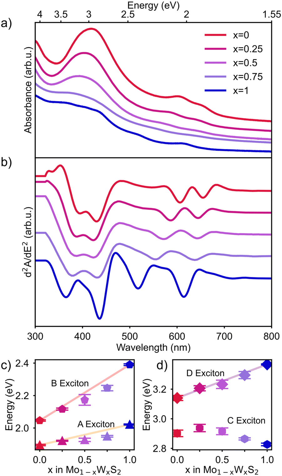 | ||
| Fig. 4 (a) Absorbance spectra (offset) of all Mo1−xWxS2 NS samples. (b) Second derivatives of absorbance spectra (offset) of Mo1−xWxS2 (x = 0–1) displaying A, B, C and D excitonic features, their composition dependent shift and the SOC related splitting of the A and B exciton. (c) Summarized positions of the A and B excitons for x = 0–1, showing a rather linear correlation with band gap bowing occurring in W-rich alloys. The error bars indicate a good reproducibility over different syntheses. (d) Shifts of the C and D exciton reveal the non-consistent behaviour of the C exciton compared to the observed trend for A, B, and D excitons. | ||
Conclusions
This study presents a wet-chemical synthesis protocol optimized for producing monolayered colloidal Mo1−xWxS2 NSs with controlled size, 2H crystal phase, and composition. The comprehensive characterization, including HAADF-STEM imaging, EDXS, Raman and absorption spectroscopy provides a thorough understanding of the structural and optical properties of the materials. Atomic-level investigation reveals tendencies for domain formation at low molar fractions in Mo1−xWxS2 alloys, especially for WS2. Further identifying the origin and parameters to control this phenomenon will enable us to suppress or encourage island formation for more complex lateral heterostructures in the future. Additionally, we have demonstrated the tunability of the band gap of colloidal Mo1−xWxS2 NSs in the range of 1.89–2.02 eV (614–655 nm), as well as the SOC related A–B exciton splitting between 0.16 and 0.38 eV. Precisely defining the absorption properties and SOC in TMDC alloys is crucial for applications, particularly in spin- and valleytronics, which have recently gained a lot of traction.Author contributions
Conceptualization: M. F. and J. L.; investigation: M. F., M. K., J. H., L. K.; data curation, visualisation, and formal analysis: M. F., M. K., J. H.; methodology: M. F., M. K.; resources: A. M., M. S., J. M., J. L. writing – original draft: M. F.; review and editing: J. H., M. S. and J. L. All authors have read and agreed to the published version of the manuscript.Conflicts of interest
There are no conflicts to declare.Acknowledgements
The authors thank André Niebur for low resolution TEM measurements. Financial support of this work has been provided by the German Research Foundation (DFG) under grant SCHE1905/9-1 (project no. 426008387), and ME3313-6 (project no. 500512256). J. L. gratefully acknowledges funding under the Excellence Strategy within the Cluster of Excellence PhoenixD (EXC 2122, Project ID 390833453) and funding by an Athene Grant of the University of Tübingen (by the Federal Ministry of Education and Research (BMBF) and the Baden-Württemberg Ministry of Science as part of the Excellence Strategy of the German Federal and State Governments).Notes and references
- M. Chhowalla, H. S. Shin, L.-J. Li, K. P. Loh and H. Zhang, Nat. Chem., 2013, 5, 263–275 CrossRef PubMed.
- S. Manzeli, D. Ovchinnikov, D. Pasquier, O. V. Yazyev and A. Kis, Nat. Rev. Mater., 2017, 2, 1–15 Search PubMed.
- K. F. Mak, C. Lee, J. Hone, J. Shan and T. F. Heinz, Phys. Rev. Lett., 2010, 105, 136805 CrossRef PubMed.
- T. Mueller and E. Malic, npj 2D Mater. Appl., 2018, 2, 1–12 CrossRef CAS.
- J. F. Gonzalez Marin, D. Unuchek, K. Watanabe, T. Taniguchi and A. Kis, npj 2D Mater. Appl., 2019, 3, 1–6 CrossRef CAS.
- J. Seo, J. H. Lee, J. Pak, K. Cho, J.-K. Kim, J. Kim, J. Jang, H. Ahn, S. C. Lim, S. Chung, K. Kang and T. Lee, Adv. Sci., 2021, 8, 2102437 CrossRef CAS PubMed.
- L. Wang, L. Huang, W. C. Tan, X. Feng, L. Chen, X. Huang and K.-W. Ang, Small Methods, 2018, 2, 1700294 CrossRef.
- T. F. Jaramillo, K. P. Jørgensen, J. Bonde, J. H. Nielsen, S. Horch and I. Chorkendorff, Science, 2007, 317, 100–102 CrossRef CAS PubMed.
- R. Kumar, W. Zheng, X. Liu, J. Zhang and M. Kumar, Adv. Mater. Technol., 2020, 5, 1901062 CrossRef CAS.
- W. Yan, O. Txoperena, R. Llopis, H. Dery, L. E. Hueso and F. Casanova, Nat. Commun., 2016, 7, 1–6 Search PubMed.
- T. Cheiwchanchamnangij and W. R. L. Lambrecht, Phys. Rev. B: Condens. Matter Mater. Phys., 2012, 85, 205302 CrossRef.
- T. Goswami, H. Bhatt, K. J. Babu, G. Kaur, N. Ghorai and H. N. Ghosh, J. Phys. Chem. Lett., 2021, 12, 6526–6534 CrossRef CAS PubMed.
- S. H. Aleithan, M. Y. Livshits, S. Khadka, J. J. Rack, M. E. Kordesch and E. Stinaff, Phys. Rev. B, 2016, 94, 035445 CrossRef.
- J. Hong, M. Koshino, R. Senga, T. Pichler, H. Xu and K. Suenaga, ACS Nano, 2021, 15, 7783–7789 CrossRef CAS PubMed.
- A. Niebur, A. Söll, P. Haizmann, O. Strolka, D. Rudolph, K. Tran, F. Renz, P. Frauendorf, J. Hübner, H. Peisert, M. Scheele and J. Lauth, Nanoscale, 2023, 15, 5679–5688 RSC.
- Y. Chen, J. Xi, D. O. Dumcenco, Z. Liu, K. Suenaga, D. Wang, Z. Shuai, Y.-S. Huang and L. Xie, ACS Nano, 2013, 7, 4610–4616 CrossRef CAS PubMed.
- D. Y. Qiu, F. H. da Jornada and S. G. Louie, Phys. Rev. Lett., 2013, 111, 216805 CrossRef PubMed.
- H. M. Hill, A. F. Rigosi, C. Roquelet, A. Chernikov, T. C. Berkelbach, D. R. Reichman, M. S. Hybertsen, L. E. Brus and T. F. Heinz, Nano Lett., 2015, 15, 2992–2997 CrossRef CAS PubMed.
- A. Chaves, J. G. Azadani, H. Alsalman, D. R. da Costa, R. Frisenda, A. J. Chaves, S. H. Song, Y. D. Kim, D. He, J. Zhou, A. Castellanos-Gomez, F. M. Peeters, Z. Liu, C. L. Hinkle, S.-H. Oh, P. D. Ye, S. J. Koester, Y. H. Lee, P. Avouris, X. Wang and T. Low, npj 2D Mater. Appl., 2020, 4, 1–21 CrossRef.
- A. F. Rigosi, H. M. Hill, K. T. Rim, G. W. Flynn and T. F. Heinz, Phys. Rev. B, 2016, 94, 75440 CrossRef.
- M. Nasilowski, B. Mahler, E. Lhuillier, S. Ithurria and B. Dubertret, Chem. Rev., 2016, 116, 10934–10982 CrossRef CAS PubMed.
- B. Mahler, V. Hoepfner, K. Liao and G. A. Ozin, J. Am. Chem. Soc., 2014, 136, 14121–14127 CrossRef CAS PubMed.
- Y. Sun, K. Fujisawa, Z. Lin, Y. Lei, J. S. Mondschein, M. Terrones and R. E. Schaak, J. Am. Chem. Soc., 2017, 139, 11096–11105 CrossRef CAS PubMed.
- Y. Sun, K. Fujisawa, M. Terrones and R. E. Schaak, J. Mater. Chem. C, 2017, 5, 11317–11323 RSC.
- G. Pippia, A. Rousaki, M. Barbone, J. Billet, R. Brescia, A. Polovitsyn, B. Martín-García, M. Prato, F. De Boni, M. M. Petrić, A. Ben Mhenni, I. Van Driessche, P. Vandenabeele, K. Müller and I. Moreels, ACS Appl. Mater. Interfaces, 2022, 5, 10311–10320 CAS.
- A. P. Frauendorf, A. Niebur, L. Harms, S. Shree, B. Urbaszek, M. Oestreich, J. Hübner and J. Lauth, J. Phys. Chem. C, 2021, 125, 18841–18848 CrossRef CAS.
- Y. Chen, D. O. Dumcenco, Y. Zhu, X. Zhang, N. Mao, Q. Feng, M. Zhang, J. Zhang, P.-H. Tan, Y.-S. Huang and L. Xie, Nanoscale, 2014, 6, 2833–2839 RSC.
- K. Premasiri and X. P. A. Gao, J. Phys.: Condens. Matter, 2019, 31, 193001 CrossRef CAS PubMed.
- P. Schiettecatte, S. Singh, P. Zhou and Z. Hens, Langmuir, 2023, 39, 6568–6579 CrossRef CAS PubMed.
- Y. Ding, Y. Wang, J. Ni, L. Shi, S. Shi and W. Tang, Phys. B, 2011, 406, 2254–2260 CrossRef CAS.
- Y. Yoo, Z. P. Degregorio and J. E. Johns, J. Am. Chem. Soc., 2015, 137, 14281–14287 CrossRef CAS PubMed.
- S. J. R. Tan, S. Sarkar, X. Zhao, X. Luo, Y. Z. Luo, S. M. Poh, I. Abdelwahab, W. Zhou, T. Venkatesan, W. Chen, S. Y. Quek and K. P. Loh, ACS Nano, 2018, 12, 5051–5058 CrossRef CAS PubMed.
- C. Ware, IEEE Comput. Graph. Appl., 1988, 8, 41–49 Search PubMed.
- M. Nacucchi, M. Alvisi, D. Altamura, V. Pfister, M. Re, M. A. Signore and M. V. Antisari, IOP Conf. Ser.: Mater. Sci. Eng., 2010, 7, 012020 Search PubMed.
- V. Y. Davydov, I. N. Goncharuk, A. N. Smirnov, A. E. Nikolaev, W. V. Lundin, A. S. Usikov, A. A. Klochikhin, J. Aderhold, J. Graul, O. Semchinova and H. Harima, Phys. Rev. B: Condens. Matter Mater. Phys., 2002, 65, 125203 CrossRef.
- E. F. Schubert, E. O. Göbel, Y. Horikoshi, K. Ploog and H. J. Queisser, Phys. Rev. B: Condens. Matter Mater. Phys., 1984, 30, 813 CrossRef CAS.
- B.-J. Hwang, L. S. Sarma, J.-M. Chen, C.-H. Chen, S.-C. Shih, G.-R. Wang, D.-G. Liu, J.-F. Lee and M.-T. Tang, J. Am. Chem. Soc., 2005, 127, 11140–11145 CrossRef CAS PubMed.
- D. O. Dumcenco, H. Kobayashi, Z. Liu, Y.-S. Huang and K. Suenaga, Nat. Commun., 2013, 4, 1–5 Search PubMed.
- S. Jiménez Sandoval, D. Yang, R. F. Frindt and J. C. Irwin, Phys. Rev. B: Condens. Matter Mater. Phys., 1991, 44, 3955 CrossRef PubMed.
- K. Gołasa, M. Grzeszczyk, R. Bożek, P. Leszczyński, A. Wysmołek, M. Potemski and A. Babiński, Solid State Commun., 2014, 197, 53–56 CrossRef.
- W. Zheng, Y. Zhu, F. Li and F. Huang, Photonics Res., 2018, 6, 11 Search PubMed.
- A. Berkdemir, H. R. Gutiérrez, A. R. Botello-Méndez, N. Perea-López, A. L. Elías, C.-I. Chia, B. Wang, V. H. Crespi, F. López-Urías, J.-C. Charlier, H. Terrones and M. Terrones, Sci. Rep., 2013, 3, 1–8 Search PubMed.
- C. Ramkumar, K. P. Jain and S. C. Abbi, Phys. Rev. B: Condens. Matter Mater. Phys., 1996, 54, 7921 CrossRef CAS PubMed.
- J. D. Ye, K. W. Teoh, X. W. Sun, G. Q. Lo, D. L. Kwong, H. Zhao, S. L. Gu, R. Zhang, Y. D. Zheng, S. A. Oh, X. H. Zhang and S. Tripathy, Appl. Phys. Lett., 2007, 91, 91901 CrossRef.
- T. C. O'Haver, A. F. Fell, G. Smith, P. Gans, J. Sneddon, L. Bezur, R. G. Michel, J. M. Ottaway, J. N. Miller, T. A. Ahmad, A. F. Fell, B. P. Chadburn and C. T. Cottrell, Anal. Proc., 1982, 19, 22–46 RSC.
- S. Tongay, D. S. Narang, J. Kang, W. Fan, C. Ko, A. V. Luce, K. X. Wang, J. Suh, K. D. Patel, V. M. Pathak, J. Li and J. Wu, Appl. Phys. Lett., 2014, 104, 12101 CrossRef.
Footnote |
| † Electronic supplementary information (ESI) available. See DOI: https://doi.org/10.1039/d4cp00530a |
| This journal is © the Owner Societies 2024 |