
 Open Access Article
 This Open Access Article is licensed under a
 Creative Commons Attribution 3.0 Unported Licence
Bismuth-oxide nanoparticles: study in a beam and as deposited†
M.-H.
Mikkelä
a,
M.
Marnauza
 b,
C. J. D.
Hetherington
b,
R.
Wallenberg
b,
E.
Mårsell
a,
Yen-Po
Liu
c,
A.
Mikkelsen
c,
O.
Björneholm
d,
G.
Öhrwall
a and
M.
Tchaplyguine
a
b,
C. J. D.
Hetherington
b,
R.
Wallenberg
b,
E.
Mårsell
a,
Yen-Po
Liu
c,
A.
Mikkelsen
c,
O.
Björneholm
d,
G.
Öhrwall
a and
M.
Tchaplyguine
a
aMAX IV Laboratory, Lund University, Box 118, 221 00 Lund, Sweden. E-mail: maxim.tchaplyguine@maxiv.lu.se
bnCHREM, Centre for Analysis and Synthesis, Lund University, 221 00 Lund, Sweden
cDepartment of Synchrotron Radiation, Lund University, Box 118, 221 00 Lund, Sweden
dDepartment of Physics, Uppsala University, Box 530, 7121 Uppsala, Sweden
First published on 5th March 2024
Abstract
Bi2O3 is a promising material for solid-oxide fuel cells (SOFC) due to the high ionic conductivity of some phases. The largest value is reached for its δ-phase, but it is normally stable at temperatures too high for SOFC operation, while nanostructured oxide is believed to have more suitable stabilization temperature. However, to manufacture such a material with a controlled chemical composition is a challenging task. In this work, we investigated the fabrication of nanostructured Bi2O3 films formed by deposition of free Bi-oxide nanoparticles created in situ. The particle-production method was based on reactive sputtering and vapour aggregation. Depending on the fabrication conditions, the nanoparticles contained either a combination of Bi–metal and Bi-oxide, or only Bi-oxide. Prior to deposition, the free particles were probed in the beam – by synchrotron-based photoelectron spectroscopy (PES), which allowed assessing their composition “on the-fly”. The nanoparticle films obtained after deposition were studied by PES, scanning electron microscopy, transmission electron microscopy, and electron diffraction. The films' chemical composition, grain dimensions, and crystal structure were probed. Our analysis suggests that our method produced Bi-oxide films in more than one polymorph of Bi2O3.
Introduction
In recent years, bismuth oxide has attracted significant attention1–4 motivated by a search for materials for the cathodes of solid-oxide fuel cells (SOFC). One of the Bi-oxide phases, its δ-polymorph, has extraordinarily high ionic conductivity, and β- and γ-phases are also ionic conductors. In general, ionic conductivity is considered high when it is ≥10−4 Ohm−1 cm−1, yet for δ-Bi2O3, it is ≈1 Ohm−1 cm−1. This value is about four orders of magnitude larger than that for the α-phase. Unfortunately, among the Bi2O3 polymorphs it is the α-phase with a monoclinic crystal structure that occurs naturally under ambient conditions. Pure δ-Bi2O3 normally exists at elevated temperature, and upon cooling it transforms into the α-phase. Moreover, while the high conductivity of δ-Bi2O3 is achieved at about 750 °C, the working temperature of SOFC is below 500 °C.5The particular feature of δ-Bi2O3 is the fcc lattice where two of eight oxygen sites are vacant in the unit cell.6 It is due to these mobile oxygen vacancies that the high ionic conductivity is realized. In general, the variety of properties of different Bi2O3 polymorphs is vast and their dependence on temperature is strong. For example, the natural α-phase exhibits p-type electronic conductivity at room temperature and becomes an n-type semiconductor between 550 °C and 650 °C. At the same time, as mentioned above, in the β- and γ- δ-phases, it is the ionic and not the electronic conductivity which prevails at room temperature.7,8
There is one more variable to consider from the point of view of SOFC: the cathodes are usually nanostructured in order to increase the surface area that can interact with oxygen, and the smaller the grain size the better it is. Moreover, it has been shown that the use of nanostructures caused a significant reduction in the temperature at which the δ-phase can be fabricated and sustained: δ-Bi2O3 nano-wires were produced at 250 °C9 and nanocrystalline δ-Bi2O3 at 200 °C.10 However, to manufacture such ananostructured material with a stable chemical composition is a challenging task: the high oxygen mobility also means the volatility of its bonding to Bi.
Wet chemistry demonstrated the ability to create nano-structured cathodes out of Bi2O3 which could be transformed to its δ-phase by high-temperature treatment.4,11 Such treatment is also needed to sinter the precipitation grains into a solid piece, providing good contact between the grains.12 The sintering, however, leads to the undesirable agglomeration of the grains into larger particles.12 Moreover, the conductivity is hindered by passivators, which envelope the grains after the growth is terminated at a planned stage. Clearly, it would be desirable to have a fabrication method not demanding passivation and sintering. In this work, we have investigated the possibility of fabricating nanostructured Bi-oxide films by depositing preformed free Bi-oxide nanoparticles created using reactive sputtering and vapour aggregation. With such a fabrication approach, only oxide-constituting ingredients were involved. As the main probing method, we used core-level photoelectron spectroscopy (PES) which is uniquely sensitive to the local environment, and, consequently, to the oxidation state and its polymorphs. Our PES results revealed the possibility of (1) creating different Bi-oxide polymorphs and (2) preserving them in the deposition. The films of deposited particles were also characterized by scanning electron microscopy (SEM), high-resolution transmission electron microscopy (HRTEM), and TEM-based selected-area electron diffraction (SAED). The microscopy and SAED revealed more details on the particle size, crystallinity, morphology of the deposited films, and the impact of the probing methods.
Experiment
A. Nanoparticle fabrication
Bismuth-oxide nanoparticles were produced using an experimental setup, which consisted of several vacuum chambers enclosing the fabrication and analysis equipment (Fig. 1). One of the chambers incorporated an in-house built nanoparticle “source” based on vapour aggregation and magnetron sputtering.13,14 For producing the parent metal vapour, a Bi target (a disc of a 50 mm diameter and 6 mm thickness) was sputtered in a magnetron DC-discharge in rarefied argon. In the “source”, the magnetron gun was placed inside a liquid–nitrogen-cooled cryostat, in which the Bi atomic vapour underwent aggregation into free nanoparticles in collisions with Ar and with the inserted from a separate inlet He. Typical input pressures for both Ar and He were from ∼5 to ∼10 mbar. Using only the Ar–He mixture, purely metallic-Bi particles were produced. For fabricating Bi-oxide particles, O2 gas was admixed into Ar, thus, reactive sputtering was realized. The O2 fraction possible to use occurred to be limited: at ∼4% O2 in Ar, a strong decrease in the sputtering rate was observed. It was assigned to the so-called poisoned state of the magnetron target.15 (See Appendix for details) As a result, O2/Ar ratios in the 1÷4% interval could be tested for the oxide-particle fabrication.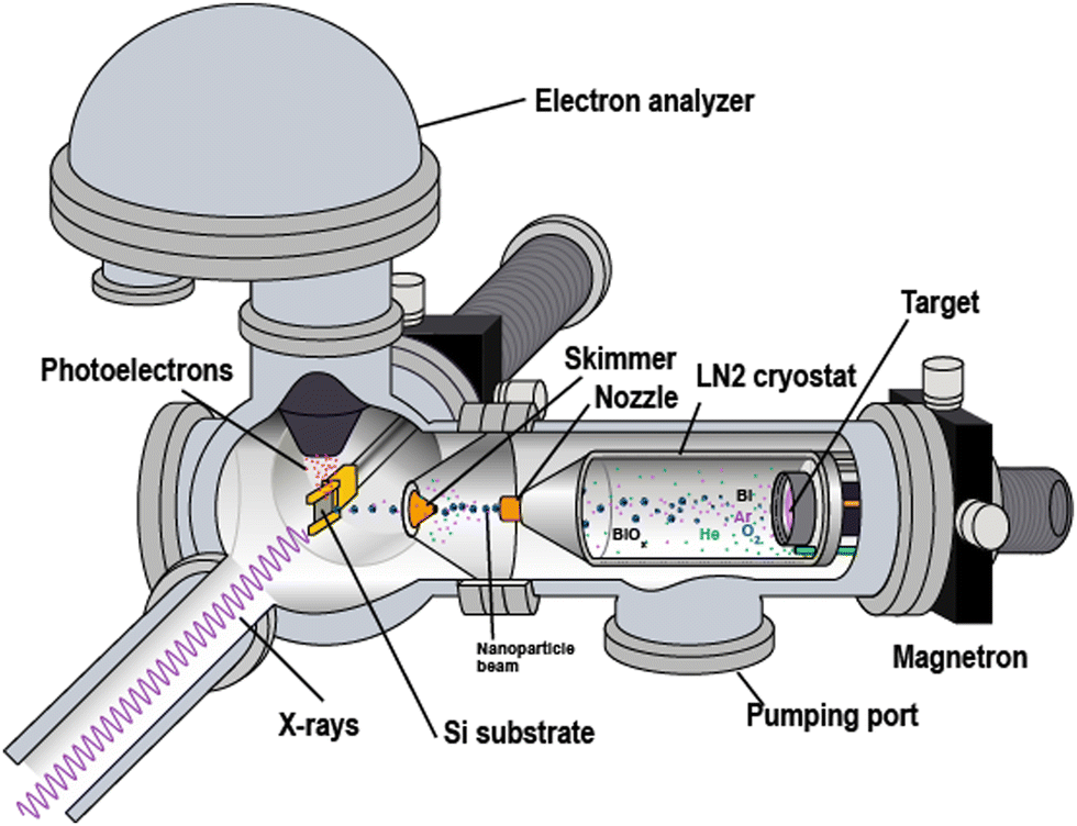 | ||
| Fig. 1 Schematic view of the experimental setup at the beamline. The particle flow out from the cryostat is directed from the right to the left. | ||
The gas flow from the cryostat into vacuum took the particles through a copper nozzlemounted at the cryostat's tip (Fig. 1). Thus a particle beam was formed. The nozzle had a 30 mm long cylindrical channel of a 2 mm diameter. Before entering the analysis vacuum chamber, the beam passed through a conical skimmer with a 2 mm orifice. This skimmer orifice was the only connection between the volumes of the source and of the analysis chamber, and 2–3 orders better vacuum could be sustained in the analysis chamber. The cryostat mounting on an XYZ manipulator facilitated the alignment of the nozzle against the skimmer, with the two typically separated by ∼5 mm. Our earlier studies on the oxide particles, created by the setup described above, showed that by changing the O2-to-Ar ratio, the method allowed producing particles of different compositions: (1) purely metallic; (2) containing both a metallic and an oxide part, or (3) fully oxidized particles. Moreover, the oxide fraction in the particles of mixed composition (type 2) could be varied. In the mixed-composition case, the metal and the oxide parts were shown to be radially segregated with the oxide forming the core and the metal – the surface shell.13,14,16,17 We assigned this segregation and structure to be driven by the relation between the cohesive energies of the metal and its oxide. Another reason for the core-shell geometry is that, in reactive sputtering, the vapour oxidation occurs mostly close to the target where the plasma is localized, and where dissociated and ionized oxygen is produced. Thus, with the distance from the target, the concentrations of metal atoms and oxide molecules change in the favour of the former, so that in the aggregation process outside the plasma volume, the particles get covered mostly by metal. (See the Appendix for details.) Under our typical fabrication conditions, the metallic shell of various meatl-oxide particles consisted of few monolayers.13,14,16,17 A similar component distribution could be expected for the Bi-oxide particles created in the present work. As shown in detail in the Results section below, the nanoparticles possessing both metallic and oxidised Bi were formed at the oxygen fraction of ≤2%. In work,10 in which conventional reactive sputtering was used for Bi-oxide film fabrication, such oxygen fraction also led to the presence of both metallic and oxidized Bi in the films. Apart from the mixed-composition possibility, our present results show that the “low” O2 fraction likely leads to Bi–O coordination that is distinctly different from that in the fully oxidized particles produced with “high” O2 values. The corresponding discussion below analyses the observed differences with respect to the various Bi-oxide phases.
B. PES, SEM, HRTEM, and SAED of nanoparticles
PES investigations for both unsupported (free) and supported (deposited) species were carried out using the X-ray light at the I41118,19 beamline, and some – at the FlexPES beamline20 at the MAX IV laboratory, Sweden. The same setup (Fig. 1) was used in both cases.The photoelectron spectra were recorded using a Scienta R4000 electrostatic electron-energy analyser mounted on the analysis chamber rotatable from 0° to 90° around the horizontally polarized X-ray beam. For the measurements on the beam of free particles, the Scienta analyser was placed at the so-called “magic” angle (54.7°) to the horizontal polarization plane. The deposited particles were studied with the analyser at either 54.7° or 90.0°.
The PES studies were performed in several binding energy regions. The Bi 5d spectra were collected in the range from 25 to 36 eV relative to vacuum. For the PES on free particles in this region, hν = 60 eV was used, leading to ≈0.15 eV total instrumental broadening. The Bi 4f spectra were recorded between 158 and 172 eV relative to vacuum. For the studies of free particles in the latter interval, hν = 215 eV was chosen, and ≈0.2 eV instrumental broadening was the result. The valence spectra of the free particles were recorded at hν = 40 eV, with ≈0.2 eV broadening. (See the Appendix for the choice of energies.) The O 1s level of the free particles could not be reliably studied because of the weak response. All spectra of the free particles were calibrated in absolute binding energy – relative to the vacuum level – using the Ar 3s line at 29.24 eV21,22 and the Ar 3p3/2 line at 15.76 eV.23 At the moment of ionization, the free particles had no contact with the analyser, so their Fermi levels were not aligned with the analyser Fermi level, in contrast to what is the case for supported samples.24 The vacuum levels of the free Ar atoms and of the nanoparticles in the beam were assumed to be the same. For the PES on the supported particles, the free ones were deposited onto a naturally oxidized Si(111)-wafer kept at T ≈ 300 K and mounted on a dedicated XYZ manipulator. The photon-beam incidence angle was ∼15° to the substrate. Then, Bi 5d and the valence spectra were collected at hν = 215 eV, with ≈0.1 eV broadening. The Bi 4f spectra for the supported particles were typically recorded at hν = 340 eV, with ≈0.1 eV broadening. (See the Appendix for the photon energy choice.) For assessing the component distribution in the particles, a limited number of the 4f spectra were recorded at 400 eV and 750 eV at the FlexPES beamline, see the Appendix for these spectra. For the deposited particles, the valence, 5d, and 4f spectra were energy-calibrated relative to the silicon Fermi edge using the Si 2p3/2 line taken at 99.45 eV (reported for a p-type doped Si(111) surface25). The O 1s region for the deposited particles was obscured by the signal from the Si-oxide formed on the substrate surface and was not used for the analysis.
All core-level spectral “lines” were fitted in Igor Pro software with the SPANCF macro package,26 using symmetric Voight profiles. It should be noted that each “line” consists of multiple subcomponents originating from a certain nanoparticle size distribution and from different local geometrical sites (e.g. surface/bulk). However, for Bi and its oxides, this substructure did not obviously manifest itself in the “line” spectral profiles. We assign it to the realized particle size (see below): the spread of the substructure “lines” occurs to be small27,28 and is convoluted into a smooth profile that is related to the life-time width and the instrumental broadening caused by the analyser and the X-ray radiation source. Thus, for simplicity, a single “line” was used in the fitting of each core-level spectral feature, and this was assumed to give an adequate description of the photoelectron spectra.
In view of the short time until a Bi-target is “sputtered through” to the backing plate and because of the relatively long time required for collecting Bi 4f spectra of the free particles, the experiments on the free and deposited species were carried out at separate occasions. The comparability of these two measurement series was ensured by using similar nanoparticle-source parameters in both cases and by assessing the nanoparticle composition prior to deposition – in the beam, on-the-fly. For that, the Bi 5d spectra were used being intense enough for a fast acquisition.
The preliminary PES investigation of the bare Si substrate plates showed them being covered by a few monolayers of Si oxide and by adsorbed carbon-containing compounds.
The deposition times, controlled either by rotation of the sample holder or by a leaf-shutter, did not exceed 3 seconds.
SEM, HRTEM, and SAED studies were carried out ex situ – on the samples produced at ≈2% and ≈4% O2 in the Ar–O2 sputtering mixture. The samples were transferred in air to the corresponding facilities. The SEM images were taken using a Hitachi SU8010 scanning electron microscope at Lund University NanoLab, Sweden. High-resolution TEM imaging and SAED were performed using a JEOL 3000F microscope at The Centre for Analysis and Synthesis, nCHREM, Lund University, Sweden.
Results and discussion
A. Nanoparticles in a beam: core-level PES spectra and oxide shifts
As stated in the Experiment section, the binding energies of the free particles were calibrated relative to the vacuum level, so they included the Fermi-energy part. Knowing binding energies of a bi-component sample relative to the vacuum level can help disclosing the component distribution, as, for example, our studies on Na–K alloys29 and oxide particles have shown. When the particles have both a metallic and an oxide part, a core-level spectrum of such particles typically contains well-separated responses of both parts.13,14,16,17 These two parts are in contact so that their Fermi levels are aligned.24 Then, with both the metal and its oxide responses in one spectrum, the oxide shift can be given a clear definition and can be accurately deduced – as the difference between the core-level energies for the metallic and the oxide parts. For the fully oxidized particles, the situation is more complex, and its peculiarities are discussed below and in detail in the Appendix. The Bi 4f and 5d core-level photoelectron spectra of the free nanoparticles, formed at four different conditions, are shown in Fig. 2. The high degree of aggregation is evidenced by the absence of the atomic-Bi spectral response well-known in its 4f and 5d energy intervals.27 The barely visible spectral features in the atomic-Bi 5d region (between 34 and 36 eV) originated from the Ar 3s satellites.22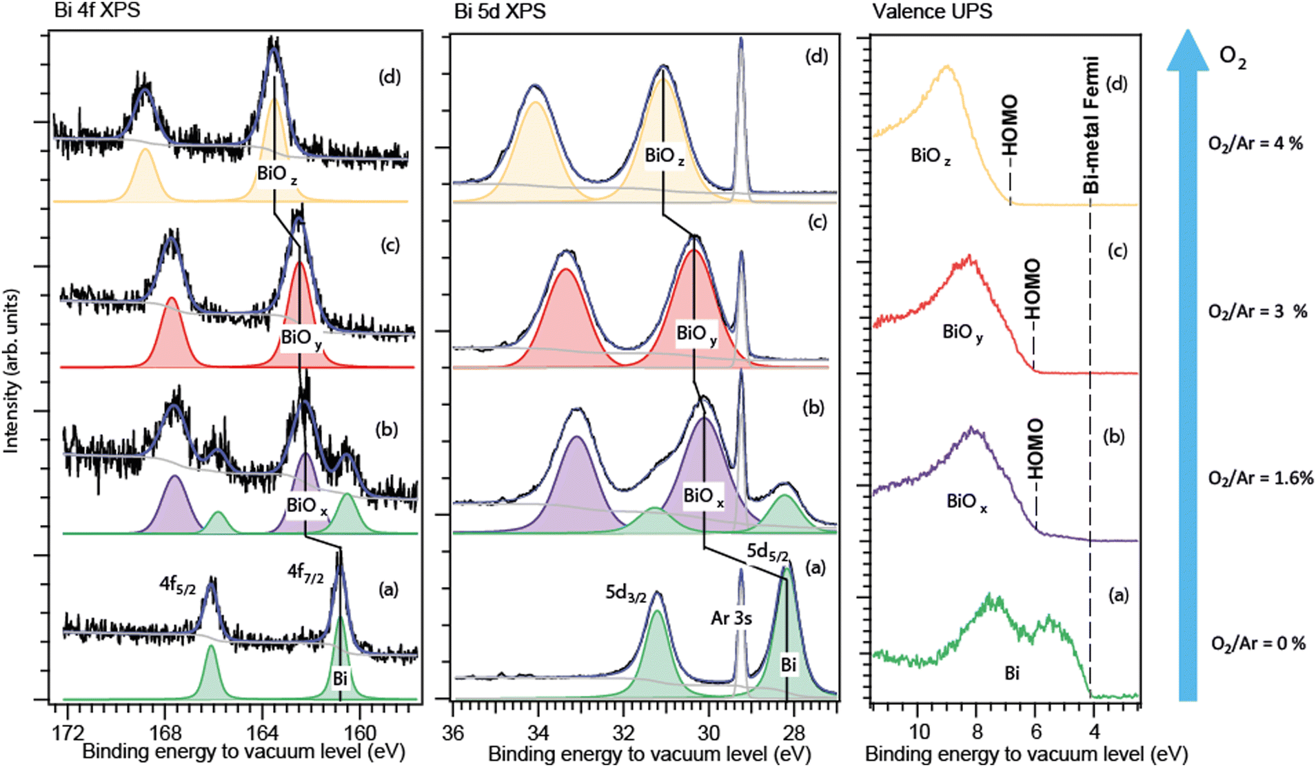 | ||
| Fig. 2 Core-level 4f (left), 5d (centre) and valence (right) PES spectra of free metallic Bi (a), Bi/Bi-oxide (b) and Bi-oxide nanoparticles (c) and (d) formed at different oxidation conditions. The sub-index “x”, “y”, or “z” denotes the varying particle composition. Energy calibration is relative to the vacuum level. | ||
The spectra of the particles produced without O2 in Ar (Fig. 2a) contain a doublet, which is characteristic of the bulk Bi–metal 4f and 5d states that are split into two spin–orbit components. The close vicinity of the measured binding energies (Fig. 2a) to those of the macroscopic Bi–metal confirmed the expectations of the Bi particles being metallic in this case. Indeed, we recorded the 4f7/2 line at ≈161 eV relative to vacuum, while for the macroscopic Bi metal, it appears at ≈157 eV30–32 relative to the Fermi edge. The metallic-Bi Fermi energy of ≈4 eV33 should be added to 157 eV to recalculate to vacuum - making it 161 eV. For the Bi 5d5/2 level of the free particles formed in the absence of oxygen, the 28.2 eV relative to vacuum was derived from our spectra (Fig. 2a). The metallic-Bi 55/2 energy relative to the Fermi level is ≈24 eV.34 Adding ≈4 eV Fermi energy to it gives 28 eV. At the conditions with the “low” O2 fraction in Ar (≤2%, Fig. 2b), a second doublet appeared in both the 5d and 4f regions – shifted towards the higher binding energies relative to the metallic doublet, the latter still intense in both the 5d and 4f spectra. Judging from its characteristically higher binding energies in each region, this second doublet was interpreted by us as due to the oxide part in the particles. For the “intermediate” (3%, Fig. 2c) and “high” (4%, Fig. 2d) O2 fractions, only the higher-energy, oxide doublet was detected in each region. The absence of metallic features under such conditions likely indicates that practically all bismuth atoms sputtered off the target were getting oxidized. Again, it is similar to what was seen in work10 on Bi-oxide films formed by deposition of Bi-oxide molecules produced by sputtering. There, the complete Bi-vapour oxidation was achieved when the O2 ratio in Ar exceeded 5%.
As can be seen from Fig. 2, for the particles fabricated under the same conditions, both types of spectra – the Bi 5d and 4f – were similar in layout: in metal-to-oxide separations (oxide shift) and in relative metal-to-oxide intensities. At the chosen photon energies, the 5d and 4f ionisation created photoelectrons in the kinetic-energy range where the PES probing depth practically changes little.
For case (b), the metallic 4f doublet's apparent position occurred to be by ≈0.3 eV lower in binding energy than in case (a). Such a difference between the corresponding cases (a) and (b) was not observed for the Bi 5d level. One should note here that the 5d spectra showed much better statistics and had an internal accurate calibration due to the Ar 3s line in the region, thus they can be trusted more than the 4f spectra. In any case, the difference is not a problem for extracting the oxide shift – since in each spectrum (4f and 5d) both the metallic and the oxide doublet are present. From the case-(b) spectra, the oxide shift was estimated to be ≈1.9 eV for the 5d level, and closer to 1.8 eV – for the 4f, but with a higher error for the latter. One can say that, judging from both the 5d and 4f levels, the 1.9 ± 0.2 eV shift was the case, thus with an acceptable total uncertainty of ≈10%.
For case (c), the choice of the reference value of the metal, whose signal was absent in the spectrum, creates some ambiguity. If starting again from the more statistically reliable and consistent 5d series, in which the metallic-doublet position was constant, the derived shift occurs to be 2.1 ± 0.1 eV. This value is practically within the uncertainty interval of case (b), thus likely meaning similar Bi–O coordination in cases (b) and (c). The small difference in the 5d oxide shift in case (c) vs. (b) (2.1 eV vs. 1.9 eV) can be explained by the metallic-shell absence in case (c). For the 4f spectrum in case (c), a shift similar to that of the 5d level can be derived when the metal position is taken as in case (b). Then, the shift is 2.0 ± 0.2 eV. Again, the matching between the 5d and 4f levels is satisfactory, which supports the choice of the reference metallic level from case (b): there is no reason why the oxide shifts for different core levels should be different in one and the same substance.
Finally, for the strongest-oxidation case (d), the oxide shift derived from the 5d series was 2.9 ± 0.1 eV and that from the 4f series −3.0 ± 0.2 eV (with the metal reference from (b)). Again, the matching of the values for the two levels is the case.
From the observations described above, the conclusion is the occurrence of a definite and large step – from ≈2 eV to ≈3 eV – in the oxide shift taking place between ≈3% and ≈4% O2 fractions.
B. Nanoparticles in a beam: valence PES spectra
The valence photoelectron spectra of the free nanoparticles (Fig. 2, right panel) were recorded under the same fabrication conditions as the corresponding core-level spectra. The analysis of the valence spectra allowed an independent from the core-levels insight into the particle composition. The calibration to vacuum was of crucial importance here. To make the analysis easier to follow, a more detailed and differently (to Fig. 2) arranged presentation of the valence spectra is given in Fig. 3. There, the upper panel shows the normalized to the maximum full-scale oxide spectra and the metallic-Bi spectrum (a) adjusted in intensity to the metallic part of spectrum (b) in the 4 to 6 eV range. The lower panel shows a close-up of the features at the feet of the bands, as well as a correspondingly scaled metallic-Bi spectrum (a). For case (b), the latter scaling allows for identifying the metallic 6p-band clearly in this oxide-dominated spectrum. Fig. 3 also visualizes the extraction of the HOMO-energies in each case: they are derived as a crossing point between the leading edges of the corresponding metallic and oxide bands and the background. The method gives the HOMO-energy uncertainty within a ±0.2 eV interval.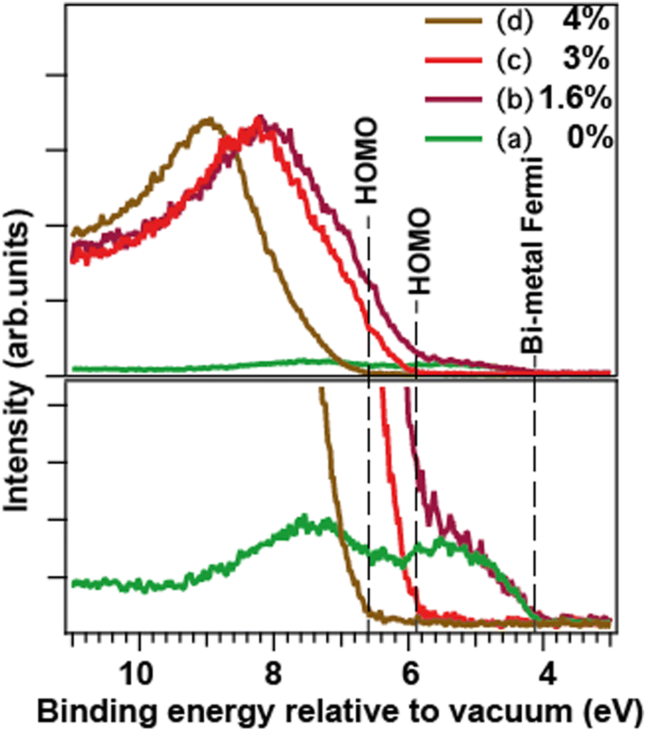 | ||
| Fig. 3 Valence spectra of the free nanoparticles formed at the same conditions as for the core-level spectra in Fig. 2. Top: Full-scale spectra, bottom: their close-up (a) metallic Bi, (b) Bi/Bi-oxide, (c) and (d) Bi-oxide nanoparticles. Spectra (b)–(d) are normalized on the maxima of the oxide features. Spectrum (a) is normalized on the maximum of Bi 6p-band in spectrum (b) at ≈5 eV. The vertical lines depict the Fermi edge of the metallic-Bi particles, and the HOMO edges for the oxides. | ||
The valence spectrum (a), recorded for the particles produced without O2 in the sputtering mixture, consisted of two main components in the 4÷10 eV interval relative to vacuum. These components had their shape and splitting (≈2 eV) similar to the valence spectra reported for various metallic-Bi solids and for supported Bi–metal nanostructures.32,35,36 This result is in accord with the understanding that the particles produced in that case were nanoscale metallic solids. The HOMO energy, which for metallic particles is also their Fermi level and work-function (WF), depends – in general – on the particle size.27,28 However, for the particles of ≈10 nm diameter, which is the case in the current work (see SEM/TEM section), the theory28 predicts that the size-related WF changes are well below the instrumental broadening. The cross-point between the leading flank in spectrum (a) and the background indicates the apparent valence-band edge, and is at ≈ 4.1 eV (Fig. 3). However, our valence spectra have ≈0.2 eV instrumental broadening, so the cross-point deconvoluted from this broadening would be correspondingly higher in binding energy. Such deconvolution makes the derived WF of the metallic particles very close to the ≈4.3 eV value for the macroscopic polycrystalline Bi WF.33
In spectra (b)–(d), the oxide creation is manifested in the presence of a feature between 6 and 11 eV binding energy relative to vacuum. As mentioned above, for the weakest oxidation condition (b), a low-intensity metallic 6p band is still visible, communicating the presence of metallic-Bi. For the stronger oxidation conditions (c) and (d), only the oxide-related features are observed. In cases (b) and (c), they are similar in shape, position, and HOMO energy (≈5.9 ± 0.2 eV for case (c)), what speaks for a similar oxide type. In case (d), the HOMO edge is by 0.7 ± 0.2 eV higher in energy than that in case (c). This can be another, independent from the core-level PES, indication of a different Bi–O coordination in cases (c) and (d). As shown further down, by combining the valence spectra for the free and for the deposited particles, the absolute Fermi energy of the two oxides (c) and (d) becomes possible to deduce.
C. Deposited particles: PES spectra and oxide shifts
The Bi 4f, 5d, and valence spectra of the deposited nanoparticles, produced initially as free with 0%, ≈2% and ≈4% O2 in Ar, are shown in Fig. 4. The spectra are calibrated to the elemental-Si Fermi level (≈2.9 eV from vacuum) which is used as zero of the energy scale. As can be seen from the comparison with Fig. 2, the spectral layouts for the deposited particles were close to those for the corresponding free ones. Indeed, for the metallic-Bi particles (Fig. 4, bottom row), a single doublet was detected in both 4f and 5d spectral regions. Furthermore, the 4f7/2 line calibrated to the Si Fermi edge gave 156.9 eV energy matching to ≈157 eV reported for the macroscopic metal.30–32 If one adds the metallic-particle Fermi energy of ≈4 eV (Fig. 2) to their 4f7/2 energy, the value becomes ≈161 eV – the same as for our free Bi particles’ spectra referenced to the vacuum level. Analogously, for the 5d level of the metallic particles, the 5d5/2 line is at 24.0 eV relative to the Fermi level, matching, for example, the value for Bi evaporated onto Ni.34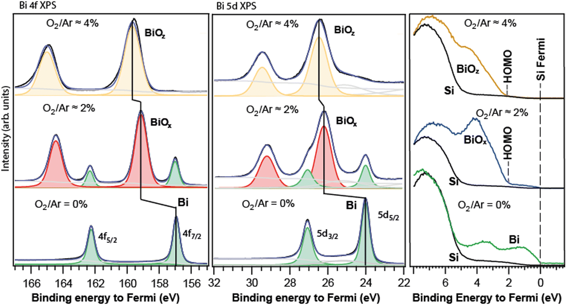 | ||
| Fig. 4 Core-level 4f (left), 5d (centre), and valence (right) PES spectra of the nanoparticle films formed by deposition of the free particles, created at similar conditions as in Fig. 2. The sub-index “x”, “y”, or “z” denotes the varying particle composition. In the valence region, the nanoparticle spectra overlap with those of the Si-substrate (black curve). The substrate's main intensity is between 5 and 8 eV relative to the Fermi level. In the 5d region, the feature between 23–25 eV is due to the O 2s response from the SiOx of the substrate. | ||
In the case with ≈2% O2, just before the deposition, the free-particles’ Bi 5d spectrum was monitored on-the-fly, and the presence of two doublets in it was established. After the deposition, the spectra of the particle film did also contain two doublets. Judging by their positions, first of all by the lower-energy doublet's energy, we assigned the doublets to the metallic Bi and Bi-oxide responses in the corresponding regions (Fig. 4, middle). Due to the presence of an internal metallic reference in the particles’ spectra, the oxide shift could be derived as the separation between the two doublets: 2.1 ± 0.1 eV for both the 4f and 5d levels. This value is practically the same as ≈2 eV for the corresponding free-particle case. One can conclude that the initial free-particle composition with the oxide shift of ≈2 eV was likely preserved in the deposition event.
In a separate experiment, under the fabrication conditions leading to two doublets in the spectra, after the deposition, we used two distinctly different photon energies −400 eV and 750 eV in PES, and the spectra showed a higher relative response of the oxide doublet for hν = 750 eV than for hν = 400 eV (see the Appendix). The 750 eV photon energy leads to a larger probing depth, so the stronger oxide response in this case is in accord with the particles having an oxide core and a metallic shell.
In the case of the strongest-oxidation conditions (≈4% O2), only one doublet was observed for the deposited particles (Fig. 4, top). The free particles were checked in the 5d region before the deposition-for showing only one high-energy doublet. As discussed earlier, the absence of metal peaks made the metal-to-oxide shift derivation not direct, and thus less certain. Taking the 4f metal at ≈157 eV and 5d at 24 eV, in the case with 4% O2 (Fig. 4, top) one gets practically the same apparent shifts for the 4f and 5d levels (within the experimental uncertainty): ≈2.6 eV for the former and ≈2.5 eV for the latter. These values are ≈0.5 eV smaller than those of the corresponding free particles. In principle, the oxide-shift decrease relative to the free-particle value could be both because of some changes in the chemical composition upon deposition, and due to the peculiarities of alignment of the Fermi level for the metallic and for the oxide particles to the Fermi level of the substrate, see below. We tend to believe that the latter reason is more likely. Indeed, for the metallic Bi-particles, the Fermi energy (≈4), which is also the HOMO energy for it, is by ≈1 eV larger than that for Si (≈2.9 eV). Upon the deposition, the absolute (vacuum-referenced) Fermi level of the Bi metal is correspondingly pulled up by this 1 eV to the Si Fermi edge, and with it, all the metallic core-levels are. The oxide-particle Fermi level is also pulled up, but by a different value – in view of a different absolute Fermi energy for the oxide. The latter can be derived via a comparison between the valence spectra of the free and deposited particles, case (d). From the valence spectra of the free particles (d), the oxide HOMO-energy is ≈6.6 ± 0.2 eV relative to vacuum (Fig. 2d, right panel). From the corresponding valence spectrum for the deposited particles (Fig. 3, top), the HOMO is ≈2 eV away from the Fermi level. The latter two facts together make the oxide Fermi energy equal to ≈4.6 eV, which is ≈0.5 eV larger than that for metallic-Bi particles. Due to that, the Fermi edge and the core-levels of the oxide particles are pulled up more than for the metallic-Bi particles – by this 0.5 eV. The ≈0.5 eV is by how much the apparent oxide shift for the deposited particles in case (d) is smaller than the shift for the corresponding free ones. Thus, the up-pulling to the substrate's Fermi level can explain the observations quantitatively and hence supports the conclusion in favour of the oxide-shift values unchanged by the deposition. Summing up the results of our PES studies on free and deposited Bi-oxide particles, one can conclude that their composition was likely preserved in the deposition. The corresponding deduced oxide shifts were then ≈2 eV and ≈3 eV with the error bars of about 10% or better.
D. Bi oxidation state, crystal phase, and the core-level PES
Since long the oxide shifts derived from photoelectron spectra were one of the main sources of information for a judgement on a metal oxidation state.37 In general, however, the oxide core-level binding energies reported in literature exhibit an often substantial spread. This introduces an uncertainty in the oxide assignment, especially if it is about fine coordination details. A common problem for extracting the oxide binding energy from a spectrum is the inaccuracy/uncertainty in the binding energy calibration. This problem is not limited to Bi oxides, but exists for PES results in general.38 In the PES on oxides, also on Bi-oxides,37,39–41 the binding energy scale was not seldom calibrated to the so-called adventitious C 1s peak, while such an approach was shown to be not particularly accurate.38 Among other factors that affect the calibration options were the peculiarities defined by the sample type: a pellet, a single crystal, a thin layer, etc. The binding energies for Bi oxides were reported for different types of samples – from single crystals and powders, to micro- and nano-structures, and for various crystal phases: α, β, δ, and γ. An overwhelming number of the works we found were on the Bi 4f state, and only a few – on the Bi 5d one, such as ref. 34 and 37. Not all of these measurements contained their own, internal reference of metallic-Bi energy, so, as discussed above, to calculate the oxide shift, we used 156.9 eV reported for the metallic-Bi 4f level most often.30–32 This value is also consistent with our own results. For the metallic-Bi 5d5/2 energy, we have used 24.0 eV from ref. 34, which value is also in accord with ours. Understandably, the studies using Al Kα (hν ≈ 1487 eV) or Mg Kα (hν = 1253.6 eV) are limited in spectral resolution: ∼1 eV instrumental broadening is not uncommon in this case.10,37,39 Moreover, in such studies, in view of the high kinetic energies of the photoelectrons, one also has to be sure that the analyser energy-scale linearity is sufficient. Indeed, the kinetic energy of the emitted Bi 4f electrons is more than 1000 eV when Mg or Al Kα are used. At such high energies, a systematic error of several tenths of eV could not be excluded. In the PES early days, however, there have not been any alternatives to Al Kα/Mg Kα, and until now instruments with such light sources are in use. One of the pioneering studies42 with Al Kα on in situ prepared Bi oxides was made on a film formed by deposition of Bi vapour thermally oxidized by O2. There, the calibration to gold 4f (84 eV binding energy) was used, which should have allowed for overcoming the energy-scale nonlinearity. The Bi 4f7/2 oxide level was reported to be at 158.8 eV, with 0.2 eV uncertainty. If one subtracts 156.9 eV for metallic Bi from it, the shift becomes ≈2 eV, which is practically the same as obtained by us for 2% O2 in the sputtering mixture. From the 5d oxide energy, also reported in work,42 a close shift value can be obtained using 24.0 eV for the metal. In that work, however, the question of the oxide crystal phase was not raised.Early studies,31 where Au 4f reference was also used, showed that “as received” commercial Bi–metal could be covered by a thin layer of oxide for which the Bi 4f shift was 1.9 eV. The metal signal, present in the spectra31 at 156.9 eV, provided an internal reference for the shift. In the same work,31 Bi-oxide powder was in situ evaporated and deposited, and the resulting films were studied by PES, with the recorded spectra again containing both the oxide and the metal responses – separated by ≈2 eV. The authors, however, did not assign the oxide to Bi2O3, but rather to a “suboxide” – BiO. Only the sample produced by exposing BiO to air at 250 °C was assigned by them to Bi2O3. For the latter, they observed the oxide binding energy corresponding to ≈3 eV shift. Although the suboxide existence cannot be excluded, the thermal treatment, which Bi-oxide underwent there – first evaporation and then annealing in air – could lead to the formation of various crystal phases, if not other substances. Their appearance was not discussed in the study.31
Another early work37 (again, with Al Kα), where now a well-defined polymorph was studied, was performed on a freshly cleaved α-Bi2O3 single crystal, thus with no internal reference. Their Bi 4f7/2 detected energy would mean ≈1.6 eV shift. This study37 reported the oxide binding energy also for Bi 5d5/2 which would give a shift of ≈1.7 eV. Although calibration on the evaporated gold was used, the uncertainties due to the resolution and charging were admitted by the authors, so the real shift values could differ somewhat from 1.6/1.7 eV calculated from their oxide energies.37
More than twenty years after the work,37 using the same spectrometer model as in ref. 37, Al Kα radiation, C 1s calibration, and an α-Bi2O3 single crystal, Bi 4f7/2 energy was measured again.39 From this, the shift of ≈1.7 eV can be derived. In view of the similar equipment, the 4f photoelectrons’ high kinetic energy, and not once mentioned sample charging, the same considerations as for work37 are valid: the uncertainty of the shift could be within some tenths of eV.
An uncommon sample preparation was used in the early work:43via α-Bi2O3 reduction by propylene. Then, 2.7 ± 0.1 eV shift towards lower energy was assigned to the transition to metal. The authors’ own metal value was by 2 eV larger than the presently accepted 156.9 eV,30–32 so was likely their oxide response: the energy calibration was probably shifted as a whole.
When a nanostructured α-Bi2O3 sample (microrods grown by thermal oxidation of Bi vapour) was studied,40 finally using synchrotron radiation with hν = 735 eV, the authors40 observed two unresolved Bi 4f doublets separated by ≈1.6 eV. The higher-energy doublet was assigned to Bi(III)-oxide, and the lower-energy one – to Bi(II)-oxide. If their Bi(III)-oxide energy is compared to that of Bi metal30–32 then the shift appears to be ≈2.3 eV. However, their lower-energy doublet was only ≈0.5 eV above the currently accepted position of the metallic-Bi doublet, which evokes doubts about their assignment. Instead, it is tempting to assign the lower-energy doublet/shoulder to the metal: the method40 could likely leave Bi partly unoxidized. The C 1s peak at 284.6 eV was used for calibration, so 0.5 eV off could be easily the case and confuse the assignment. If the lower doublet is due to the metal then their shift for α-Bi2O3 is ≈1.6 eV.
For another nanostructured-oxide – chemically grown α-Bi2O3, a relatively recent PES work44 used Mg Kα light and Au 4f for calibration. The Bi 4f energies reported give the shift of ≈1.9 eV. The oxide fabrication method in ref. 44 has been one of those typical for oxide powder production - by precipitation in wet-chemistry reactions. In one of the early works, for similarly prepared α-Bi2O3 powder samples, the reported Bi 4f oxide energy41 gives the oxide shift of ≈1.9 eV. In ref. 41, the calibration was done using the C 1s peak, then at 285 eV.
All-in-all, the analysis of a set of studies on various α-Bi2O3 (or likely α-Bi2O3) samples shows that in the majority of reliable measurements, the shift was between ≈1.6 and ≈2 eV. At the same time, in at least two early studies,31,43 the ≈3 eV shift was reported, though the sample preparation (annealing in air,31 reduction by propylene43) may have influenced the composition and calibration.
The only known to us PES study where the δ-phase was claimed and where the core-level spectra were measured is work.10 There, Mg Kα radiation was used for ionisation, and the C 1s signal at 284.6 eV – for calibration. The oxide film was prepared by RF reactive sputtering of a Bi target in the Ar–O2 mixture and deposition of the resulting vapour on a Si substrate. There, the δ-phase could be prepared only at specific conditions: at more than 5% O2 in Ar and at a substrate temperature of 200 °C. According to the X-ray diffraction (XRD) pattern, below 5% O2, the films contained metallic Bi and the β-phase oxide. When the substrate's temperature was above 200 °C only the β-phase oxide was observed. In work,10 the Bi 4f spectra were presented only for the δ-phase oxide and contained only one doublet, thus, no internal metallic reference was available. The 4f7/2 oxide binding energy in spectra10 would mean a 1.6 eV oxide shift. While the C 1s calibration used in ref. 10 is not ultimately reliable, the systematic error can hardly exceed 1 eV, so the shift value cannot be much off. If taken as it is, it occurs on the lower-limit side of the range for the α-Bi2O3 phase. One would, however, think that the α- and δ-phases should distinctly differ from each other. Indeed, the geometry and the lattice constants are very different6 for the monoclinic α-phase and for the oxygen-deficient fcc δ-phase. Chemical shifts are known to be sensitive to even such small differences in coordination as those realized for different sites in one and the same crystal. The coincidental summing up of various peculiarities in the two phases to the same shift could, in principle, happen, but would not be the first thing to expect.
Reactive sputtering of a metallic Bi target was also used for producing thin Bi2O3 films in work.45 There, however, in spite of the similarity to ref. 10, sputtering and deposition conditions (more than 10% O2 and around 200 °C of the substrate), only the β-phase oxide could be observed by XRD. The substrate was however not Si (as in ref. 10) but glass covered with indium-doped tin oxide. The conductivity of such a substrate may be not enough for photoelectron spectroscopy to avoid charging of the Bi-oxide, which is not an ideal electron conductor itself. Thus, the ≈ 1.2 eV45 shift possible to deduce from the oxide 4f spectra45 recorded with Mg Kα and 0.4 eV resolution, in the absence of internal metallic reference, may be well some tenths of eV off.
The β-phase creation was also confirmed by XRD in a work,46 where the Bi-carbonate heating to more than 600 °C in air was the first fabrication stage. After further annealing and cleaning by Ar+-sputtering, the resulting substance was probed by PES using Al Kα radiation, and C 1s peak, now at 284.8 eV, for calibration. The PES spectra of the powder pellets showed two unresolved doublets separated by ≈1 eV. The authors46 assigned the lower energy doublet to the Bi(III)-oxide in its β-phase and claimed that the binding energy for it was the same 158.1 eV as authors' value for α-Bi2O3.
The commercial pellets of the latter oxide phase were studied by them separately, without pre-treatment. Such an energy46 (158.1 eV) would mean ≈1.2 eV oxide shift for both α and β polymorphs. The higher-energy, second doublet in the spectra46 was assigned to Bi(V)-oxide. Its separation from the 157 eV metallic reference would be then just above 2 eV. It is difficult to make a judgement on the observations and assignments in work,46 not only because of the usual calibration uncertainties, but also because the doublets were not resolved, and the spectral broadening, from which the idea of the second doublet stemmed, could have been caused by many reasons, first of all by the sample charging. Additionally, the Ar-ion bombardment could have reduced the oxide to metal.46 In general, neither the work45 nor46 seem to be a source of a consistent reference for Bi2O3. However, with some assumptions and reservations, the 1.2 eV for β-Bi2O3 might be used.
The γ-phase PES study was reported in work47 where sintered and Ag+-sputtered powder pellets showed a corresponding XRD response, either as purchased or after the sputtering. The PES with Mg Kα radiation and C 1s (285.0 eV) calibration recorded two overlapping peaks for each 4f spin–orbit component. However, the values reported47 for 4f7/2 (159.4 eV) and 4f5/2 (165.0 eV) components were separated not by the typical 5.3 eV but by 5.6 eV, what evokes some doubts about the adequacy of the features’ assignment. Also, the two peaks within each spin–orbit “group” were separated by different values: ≈1.6 eV for 4f7/2 and ≈1.1 eV 4f5/2. If the 4f7/2 oxide value (159.4 eV47) were correct that would mean ≈2.5 eV for the γ-phase relative to the common 156.9 eV metallic reference. However, the metal appearance after sputtering suggests that the original signals are due to the metal and the oxide. Then, the γ-phase shift can be estimated as an average of 1.6 and 1.1: ≈1.3 ± 0.3 eV.
As described in our Experiment section, in the present work, the ≈2 eV oxide shift was derived from the spectra of the free and deposited particles formed at the low and intermediate oxidation conditions. This value is within the ≈1.6÷≈2 eV interval estimated for the α-phase from those studies, the results of which could be seen as more trustworthy. One can conclude that the probability of our such particles having the α-phase oxide composition is high.
The 1.2–1.3 eV oxide shifts, extracted by us for the β- and γ-phases from the data found in ref. 45–47 were not detected in the current work. Thus, likely, the presence of the β- and γ-phases in our samples can be excluded.
The 1.6 eV shift that was derived from the oxide binding energy reported in work,10 and assigned there to the δ-phase, was also not observed in our experiments.
If compared to the work with reactive sputtering,10,45 our case differs in the conditions of aggregation/agglomeration: it happens prior to the deposition, and, at least for the free particles, is not in any way influenced by the substrate. Moreover, in our case, during a significant part of the particle formation process, the temperature is likely high enough to provide mobility within the particle (see the Appendix). These peculiarities appear to be enough to cause the formation of phases different from work.10,45
To the best of our knowledge, the 3 eV oxide shift, derived by us for the particles formed at the strongest oxidation condition, has not been undoubtedly observed before. The two early cases considered above, one with the oxide thermal treatment in air,31 the other with the oxide reduction by propylene,43 would not stand scrutiny from the modern surface-science positions.
Among the factors which define the metal core-level shifts for different phases of an oxide is the tightness of the crystal. The core-level energy variation for a positive metal-ion in an ionic compound, such as an oxide, is defined, first of all, by the Coulombic interaction with the anion in the ionized state.48 Obviously, this interaction is strongly dependent on the separation between the ions, which in crystals is defined by the lattice constants. The smaller the constant, the larger is the change in the metal-ion core-level energy—relative to an isolate-ion case. In this respect, a comparison of the lattice constants for different phases may provide additional considerations for the shift assignment. For the δ-phase, the fcc crystal lattice constant is ≈5.6 Å.6 For all other phases, the constants are noticeably larger. Thus, for the monoclinic α-phase, the a, b, and c constants are 5.8 Å, 8,2 Å, and 7,5 Å6, correspondingly. For the bcc γ-phase, a is 10.3 Å. For the tetragonal β-phase, the a and b constants are 7.7 Å and 5.6 Å6.
Although the fine peculiarities of geometry may play an additional role in the separation between the cations and anions in a crystal, it would not be an exaggeration to say that the δ-phase fcc is by far the tightest crystal of them all. From that point of view, it is not unreasonable to expect that this phase will exhibit the largest oxide shift. In view of the difficulties in sustaining the δ-phase, it is not surprising that the larger than ≈2 eV shifts have not been as a rule observed. However, to claim the δ-phase presence in our particles without a confirmation by diffraction would be a too far going conclusion. To investigate the issue, a SAED study has been attempted in the current work, in the frames of a wider electron-microscopy characterization.
E. Deposited nanoparticles: SEM and TEM
One of the goals of the scanning electron microscopy study on the deposited particles was to obtain information on their average size and on the morphology of the films. What appeared to be possible to observe in SEM is illustrated by an image of a typical film formed by deposition of Bi-oxide particles (Fig. 5). The “parent” particles were produced at ≈4% O2 in the Ar–O2 mixture. The magnification used in the presented image allowed getting an overview of a relatively large deposition area on silicon. The image demonstrates the porosity, but, at the same time, the film's relative uniformity. These properties would be important for the design of practical devices. Higher-magnification images (not shown) allowed estimating the size to be in the range mainly between 10 and 20 nm.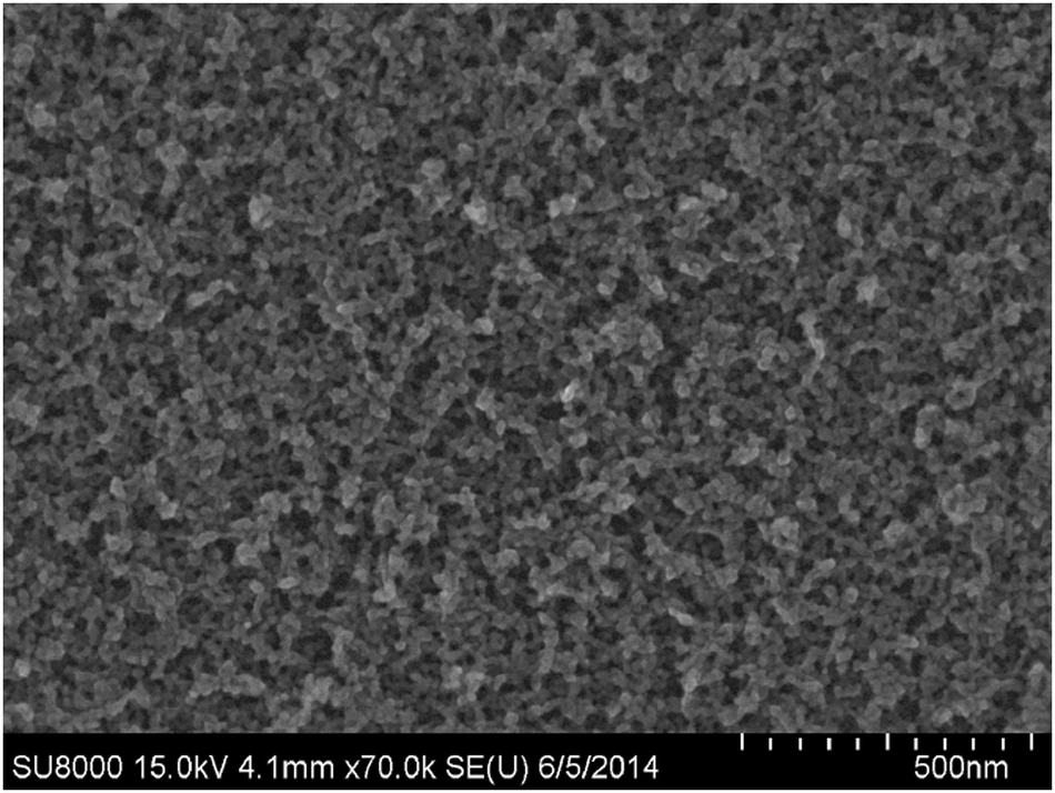 | ||
| Fig. 5 SEM image of the film formed by deposition of Bi-oxide nanoparticles. | ||
For the TEM study, the nanoparticles produced at ≈2% and ≈4% O2 in the Ar–O2 mixture were either deposited directly on a TEM grid or scraped off a silicon wafer onto a TEM grid. As can be seen from Fig. 6, exemplifying the 4% case, the dimensions of individual nanoparticles were near 10nm. Similar dimensions were observed for the particles created at other oxidation conditions. In the higher magnification images, such as the one in Fig. 6, right panel, the crystalline nature of individual nanoparticles can be observed. For the chosen small areas, which contained obviously crystalline particles, also an electron diffraction study was carried out using TEM. The analysis of diffraction patterns showed a strong presence of Bi metal. It should be mentioned, however, that at larger TEM magnifications, which implied a more energetic electron beam, the particles were seen transforming their crystal structure (but not the dimensions and positions) in real time. The presence of such a transformation raises a question of how much one can rely on the SAED results. The conclusion was that a more thorough and extensive diffraction study was necessary to be able to produce adequate and reliable sample characterization by SAED.
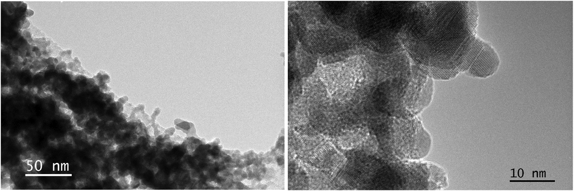 | ||
| Fig. 6 TEM of the nanoparticles produced at ≈4% O2 in the Ar–O2 sputtering mixture. Left panel: TEM image of a nanoparticle film; right panel: higher-magnification HRTEM image showing crystalline structure in individual particles. | ||
Conclusions
In the present work, an in-house-built apparatus and a method based on vapour aggregation and reactive sputtering were used to produce metallic-Bi, mixed Bi/Bi-oxide, and purely Bi-oxide free nanoparticles, as well as their films formed by the particle deposition. The sputtering-based in-vacuum fabrication allows for avoiding contaminations present in the alternative wet-chemistry methods. As a result, there is no necessity for heat treatment of the particle films, which is usually needed in wet chemistry for purification of the precipitation grains. Moreover, no sintering of such grains into interconnected structures is necessary with the method suggested.In the present work, the nanoparticles were probed by several techniques and in different environments. Free nanoparticles in a beam were characterized by PES in several binding energy regions. For that, synchrotron X-ray radiation with optimized for ionization and spectral resolution photon energies was used. The particles were also studied by PES directly after the deposition, in situ, in the form of nanoporous thin films on naturally oxidized silicon. The PES investigation allowed determining the oxide shifts and thus addressing the question of various possible oxidation states and oxide phases realized. Judging from the oxide shifts of the free particles created at lower fractions of O2 gas, they likely contained α-Bi2O3 oxide, with ≈2 eV shift. A comparison of the photoelectron spectra for the free and deposited nanoparticles supported the conclusion of the nanoparticles’ composition preservation in the deposition events. For the particles produced at a higher O2 fraction, the oxide shift of ≈3 eV could be derived. To the best of our knowledge, such a large shift has not been reliably observed before. The argument is discussed that δ-Bi2O3 can be expected to have a shift larger than the other phases, in particular larger than ≈2 eV of the α-phase. More investigation is necessary to complement the PES results with SAED.
Together, the PES and the electron microscopy results demonstrate that the nanoparticle fabrication method under discussion can be used to fabricate a nanoporous homogeneous film of crystalline ≈10 nm particles of a certain “engineered” Bi-oxide composition, likely the α-phase, but also another so far unidentified phase.
Author contributions
The manuscript was written through contributions of all authors. All authors have given approval to the final version of the manuscript. All authors contributed equally.Conflicts of interest
There is no conflict of interest.Appendix
A. Fabrication details
The method of reactive magnetron sputtering is used in industrial oxide-film production and is relatively well understood. There, the primary path of the oxide formation is via the gas-phase reactions between the individual free metal-vapour atoms and different reactive forms of oxygen (dissociated, ionised, excited). However, the metal atoms and reactive oxygen are created within the magnetron-plasma volume, which is localized to the target. Reactive sputtering allows efficiently forming oxides even of noble metals, such as silver and gold.17,49 For example, in work,49 the mass-spectroscopy detected the high abundance of AuO and AuO2 gold-oxide molecules formed in the Ar/O2 plasma. Thus formed in plasma, free oxide molecules are the precursors of either thin films (as in the conventional application of magnetron sputtering) or nanoparticles (as in our case). Not only do the free metal atoms react with oxygen, but also the metal target gets partially oxidized. As mentioned in the experimental part, this is an undesirable effect that reduces the metal sputtering rate and, as a result, the oxide-molecule production. As mentioned above, the effect is known as target “poisoning”.15For the thin-film growth, the oxide molecules are directly deposited on a substrate, while in our case, they are first let agglomerate into particles. The agglomeration is achieved by forcing the molecules to stay inside a cryostat filled with a cryogenically cold argon/helium mixture. The cryostat geometry and the Ar–He pressures in use define the so-called aggregation time. The longer the time, the larger the particles. In other words, the formation of the particles via aggregation takes place inside the cryostat, rather than due to the gas/vapour expansion into vacuum.50 The latter is the case for a supersonic jet formed at a much larger pressure difference between the gas container and the expansion volume, than in the vapour-aggregation method.
At lower concentrations of oxygen in the gas mixture, not all sputtered free metal atoms are oxidized by oxygen reactive forms. The former is then taken through the 20 cm long cryostat by the gas flow – towards the exit. At the same time, the latter are present mostly only close to the target. Thus, the oxide formation stops soon after the species leaves the dense plasma volume, which in our case ends ∼1 cm away from the target. The collisions with the cryogenically cold Ar and He atoms continue to take place along the whole path in the cryostat, thus facilitating further condensation. Towards the end of the cryostat, it is only the metal atoms which are left to participate in the aggregation. This is how a metallic shell can be formed-due to the peculiarities of the particle distribution inside the cryostat. Additionally, thermodynamics is also involved in shaping the component distribution in the particles. The latter is first formed relatively “hot”, thus with enough mobility to redistribute the components so that the particle reaches the lowest-energy state. It is then more favourable to have the substance with the higher cohesive energy in the “bulk”, and such substance is typically the oxide.
B. The choice of photon energies and related probing depth
For free nanoparticles, in view of their dilute concentration in a beam, the photon energies corresponding to the maximum of the ionization cross-section had to be used. For Bi 5d, this is ≈60 eV.51 Above it, the cross-section steeply drops by almost four orders of magnitude within the 150 eV interval.51 For Bi 4f, the maximum is near hν = 400 eV,51 however, to have photoelectron kinetic energy comparable with that of the 5d, a substantially lower photon energy had to be chosen. At the same time, the hν roughly below 200 eV would lead to the Auger features (due to Bi 5d decay) moving into the 4f spectrum. As a compromise, hν = 215 eV was used.For the deposited particles, one is forced to use hν significantly further away from the ionization threshold (than for the free particles) – to avoid the “slow” secondary electrons in the spectrum. These electrons, originating in our case not only from the ultrathin nanoparticle film but also from the massive (in comparison with the film) substrate, form a background rising towards zero kinetic energy. In the case of the Bi 5d region, again hν = 215 eV was chosen – allowing now keeping the Auger due to the 4f decay out of the spectrum: A lower hν would move the Auger features into it. A higher hν would even more change the probing depth – relative to the free-particle case. The hν = 215 eV seemed to be a reasonable compromise also in this case. To have similar kinetic energies for Bi 4f as for the 5d, hν = 340 eV was chosen for the 4f ionization. The substantially higher photon energies would increase the PES probing depth, however were not used – as the first choice, though the particle density in the films would allow it. The reason was the expected radiation damage at hν above the oxygen O 1s ionization threshold (530–540 eV). In ionic compounds, in the core-ionization process, known to be localized on individual atoms, ionization of an anion leads to a loss of its negative charge. Then, after the Auger decay, one more negative charge is unattached from the initially negative ion. In the case of Bi2O3, the oxygen atom becomes neutral after the Auger decay, so its bonding is no longer ionic and thus is weak. In turn, it can lead to a loss of the initially negatively charged ion by the sample. This phenomenon was studied for alkali-halides, in, for example, work,52 where NaCl and NaBr surfaces were “rapidly destroyed by photon-stimulated desorption of the halogen, … leading ultimately to the appearance of Na metal on the surface.” In the case of our 10 nm nanoparticles in an ultrathin film, the “surface” may mean a volume deep into a particle.
Nevertheless, in a dedicated series of measurements, using fabrication conditions that produced two 5d doublets for free particles, we deposited particles on a Si substrate and recorded their Bi 4f spectra at 400 eV and 750 eV photon energies, see Fig. 7. There, the intensity is normalized to the metallic-Bi signal (lower doublet). Comparing the spectra for hν = 400 eV, meaning 230–240 eV kinetic energies for the 4f photoelectrons, and for hν =750 eV, meaning 580–590 eV kinetic energies, one observes a definite increase of the relative oxide signal in the latter case. This is consistent with the oxide being in the particle “bulk”. The so-called “universal curve”53 for the probing depth λ (or “mean free path”) gives an approximate dependence of λ on the kinetic energy. The probing depth at 580÷590 eV kinetic energy is found to be about two times larger than for 230÷240 eV. For ≈200 eV kinetic energy, the depth is ≈8 Å, which value is close to the lattice constants in the α-phase. One should note here, that for quasi-spherical objects, by which nanoparticles can be roughly approximated, the attenuation of the photoelectron signal I depends in a more complex way54 on the depth d than for the plane layers, for which I ∼ exp(−d/λ).53 If, anyway, the universal curve is used, our probing depth occurs to be 2–3 layers at the kinetic energies in question.
 | ||
| Fig. 7 Calibrated to Fermi edge spectra of the same deposited oxide-containig particles recorded at hν = 400 eV (red) and 750 eV (black), normalized on the metallic peak. | ||
C. Energy reference and the binding energy shifts in PES
In PES on supported samples, the sample is in contact with the analyser, and ideally, the sample Fermi level is aligned to that of the support/substrate, and the Fermi level of the latter is aligned to that of the electron energy analyser. As a result, it is usual to refer/calibrate the core-level spectra to the common Fermi level, the absolute value for the substrate is typically known. For the metals, this means that the reported binding energy value usually excludes the Fermi level/work-function of the sample. For the metals, such calibration is straightforward because of two reasons. First, there are electrons at the Fermi levels of a metal, so this level is directly observable in the spectrum as a rise of the valence band. Second, the metal conductivity is so high that the electrons being continuously lost due to the ionization are “instantaneously” replaced by the substrate electrons. Both circumstances are generally not the case for semiconductors and isolators. There are no electrons at their Fermi edge, so it is not seen in the photoionization spectra and its absolute energy (relative to vacuum) is a priori unknown. As for its alignment with the Fermi energy of the substrate, it may not be the case also. The loss of electrons under ionizing radiation is compensated only at a certain rate (depending on conductivity), which may be not enough to completely avoid a permanent charge of the sample. This is analogous to a diode, in which the Fermi level alignment, existing with equal potentials on both sides, disappears when one of the sides is biased.In contrast, free nanoparticles have no contact with the experimental setup, so, as a consequence, the Fermi-levels of such particles are not aligned with the Fermi-level of the electron analyser. The remaining alternative for determining the core-level binding energy of the free particles is to measure it relative to the vacuum level, thus including the Fermi-energy part.
With the chemical state change, like oxidation, two types of binding energy changes may transform the vacuum-referenced core-level energies of free nanoparticles: (1) the core-level shift relative to the nanoparticle Fermi-level – just like for the supported samples, which shift can be referred to as the core-Fermi shift; and (2) the sample Fermi-level shift relative to the vacuum level, which can be referred to as Fermi-vacuum shift. A change similar to the latter change happens also as a result of oxide-particle deposition: the Fermi-vacuum shift changes from that being equal to the oxide Fermi energy to that equal to the substrate Fermi energy. This is what we have discussed in connection with the Bi-oxide spectra for the strongest oxidation case. In general, the issue deserves a separate detailed discussion.
Acknowledgements
This work has been financially supported by the Swedish Research Council (VR), the European Community's Seventh Framework Programme (FP7/2007-2013) under grant agreement number226716, the Knut and Alice Wallenberg Foundation (KAW), the Göran Gustafsson Foundation, and the Carl Trygger Foundation. We acknowledge the staff of MAX-lab for their assistance during the experiments. We acknowledge financial support from NanoLund and by nCHREM, Centre for Analysis and Synthesis, Lund University.References
- J. Hou, L. Bi, J. Qian, Z. Zhu, J. Zhang and W. Liu, J. Mater. Chem. A, 2015, 3, 10219 RSC.
- J. Hou, L. Bi, J. Qian, Z. Gong, Z. Zhu and W. Liu, J. Power Sources, 2016, 301, 306 CrossRef CAS.
- N. Ai, N. Li, S. He, Y. Cheng, M. Saunders, K. Chen, T. Zhang and S. P. Jiang, J. Mater. Chem. A, 2017, 5, 12149 RSC.
- Y.-L. Huang, A. M. Hussain and E. D. Wachsman, Nano Energy, 2018, 49, 186 CrossRef CAS.
- Y. Zhang, R. Knibbe, J. Sunarso, Y. Zhong, W. Zhou, Z. Shao and Z. Zhu, Adv. Mater., 2017, 29, 1700132 CrossRef PubMed.
- H. A. Harwig, Anorg. Z. Allg. Chem., 1978, 444, 151 CrossRef CAS; H. A. Harwig and A. G. Gerards, Thermochim. Acta, 1979, 28, 121 CrossRef.
- S. F. Radaev, V. I. Simonov and Yu. F. Kargin, Acta Crystallogr., Sect. B: Struct. Sci., 1992, 48, 604 CrossRef.
- F. M. A. Aguirre and R. H. Becerra, Appl. Phys. A: Mater. Sci. Process., 2015, 119, 909 CrossRef.
- C. C. Huang, I. C. Leu and K. Z. Fung, Electrochem. Solid-State Lett., 2005, 8, 204 CrossRef.
- H. T. Fan, S. S. Pan, X. M. Teng, C. Ye, G. H. Li and L. D. Zhang, Thin Solid Films, 2006, 513, 142 CrossRef CAS.
- B. Yu, C. Zhu and F. Gan, J. Appl. Phys., 1997, 82, 4532 CrossRef CAS.
- Y.-L. Huang, A. M. Hussain, I. A. Robinson and E. D. Wachsman, ACS Appl. Mater. Interfaces, 2018, 10, 28635 CrossRef CAS.
- C. Zhang, T. Andersson, S. Svensson, O. Björneholm and M. Tchaplyguine., Phys. Rev. B: Condens. Matter Mater. Phys., 2013, 87, 035402 CrossRef.
- M. Tchaplyguine, M.-H. Mikkela, C. Zhang, T. Andersson and O. Björneholm, J. Phys. Chem. C, 2015, 119, 8937 CrossRef CAS.
- S. Berg and T. Nyberg, Thin Solid Films, 2005, 476, 215 CrossRef CAS.
- C. Wright, C. Zhang, M.-H. Mikkelä, E. Mårsell, A. Mikkelsen, S. Sorensen, O. Björneholm and M. Tchaplyguine, J. Phys. Chem. C, 2017, 121, 19414 CrossRef CAS.
- M. Tchaplyguine, M.-H. Mikkela and O. Björneholm, Multi-component nanoparticles for novel technologies, in 21st Century Nanoscience—A Handbook, ed. K. Sattler, Taylor & Francis, 2020 Search PubMed.
- M. Bässler, J.-O. Forsell, O. Björneholm, R. Feifel, M. Jurvansuu, S. Aksela, S. Sundin, S. L. Sorensen, R. Nyholm, A. Ausmees and S. Svensson, J. Electr. Spectrosc., 1999, 101, 953 CrossRef.
- M. Bässler, A. Ausmees, M. Jurvansuu, R. Feifel, J.-O. Forsell, P. de Tarso Fonseca, A. Kivimäki, S. Sundin, S. L. Sorensen, R. Nyholm, O. Björneholm, S. Aksela and S. Svensson, Nucl. Instrum. Methods, 2001, 469, 382 CrossRef.
- A. Preobrajenski, A. Generalov, G. Öhrwall, M. Tchaplyguine, H. Tarawneh, S. Appelfeller, E. Frampton and N. Walsh, J. Synchrotron Rad, 2023, 30, 831 CrossRef CAS PubMed.
- Y. Ralchenko, A. E. Kramida, J. Reader and NIST ASD Team, NIST Atomic Spectra Database ver.4.1.0, National Institute of Standards and Technology, Gaithersburg, MD, 2011 Search PubMed.
- A. Kikas, S. J. Osborne, A. Ausmees, S. Svensson, O.-P. Sairanen and S. Aksela, J. Electr. Spectrosc. Rel. Phenom., 1996, 77, 241 CrossRef CAS.
- I. Velchev, W. Hogervorst and W. J. Ubachs, J. Phys. B: At. Mol. Opt. Phys., 1999, 32, L511 CrossRef CAS.
- W. F. Egelhoff, Jr., Surf. Sci. Rep., 1987, 6, 253 CrossRef.
- R. D. Bringans, M. A. Olmstead, R. I. G. Uhrberg and R. Z. Bachrach, Phys. Rev. B: Condens. Matter Mater. Phys., 1987, 36, 9569 CrossRef CAS PubMed.
- Spectrum Analysis by Curve Fitting (SPANCF) macro packages for Igor Pro software by E. Kukk (edwin.kukk@utu.fi), University of Turku, Finland.
- M.-H. Mikkelä, M. Tchaplyguine, S. Urpelainen, K. Jänkälä, O. Björneholm and M. Huttula, J. Appl. Phys., 2012, 112, 084326 CrossRef.
- M. Seidl, J. P. Perdew, M. Brajczewska and C. Fiolhais, J. Chem. Phys., 1998, 108, 8182 CrossRef CAS.
- M. Tchaplyguine, S. Legendre, A. Rosso, I. Bradeanu, G. Öhrwall, S. E. Canton, T. Andersson, N. Mårtensson, S. Svensson and O. Björneholm, Phys. Rev. B: Condens. Matter Mater. Phys., 2009, 80, 033405 CrossRef.
- J. F. Moulder, in Handbook of X-ray Photoelectron Spectroscopy, ed. J. Chastain, Physical Electronics Devision, PerkinElmer Corp., 1992 Search PubMed.
- V. S. Dharmadhikari, S. R. Sainkar, S. Badrinarayan and A. Goswami, J. Electr. Spectrosc., 1982, 25, 181 CrossRef CAS.
- P. J. Kowalczyk, O. Mahapatra, D. N. McCarthy, W. Kozlowski, Z. Klusek and S. A. Brown, Surf. Sci., 2011, 605, 659 CrossRef CAS; P. J. Kowalczyk, D. Belic, O. Mahapatra, S. A. Brown, E. S. Kadantsev, T. K. Woo, B. Ingham and W. Kozlowski, Appl. Phys. Lett., 2012, 100, 151904 CrossRef.
- in CRC Handbook of Chemistry and Physics (Internet Version 2020), ed. W. M. Haynes, CRC Press, Taylor & Francis, Boca Raton, FL, 101st edn, 2020https://www.hbcponline.com Search PubMed.
- K. Guertler, K. H. Tan, G. M. Bancroft and P. R. Norton, Phys. Rev. B: Condens. Matter Mater. Phys., 1987, 35, 6024 CrossRef PubMed.
- A. Kakizaki, M. Niwano, H. Yamakawa, K. Soda, S. Suzuki, H. Sugawara, H. Kato, T. Miyahara and T. Ishii, J. Phys. F: Met. Phys., 1988, 18, 2617 CrossRef CAS.
- Y. Baer and H. P. Myers, Solid State Commun., 1977, 21, 833 CrossRef CAS.
- T. P. Debies and J. W. Rabalais, Chem. Phys., 1977, 20, 277 CrossRef CAS.
- G. Greczynski and L. Hultman, Prog. Mater. Sci., 2020, 107, 100591 CrossRef CAS.
- Y. A. Teterin, K. E. Ivanov, A. Yu. Teterin, A. M. Lebedev, I. O. Utkin and L. Vukchevich, J. Electron Spectrosc., 1999, 101–103, 401 CrossRef CAS.
- M. Vila, C. Diaz-Guerra and J. Piqueras, J. Alloys Compd., 2013, 548, 188 CrossRef CAS.
- Y. Schuhl, H. Baussart, R. Delobel, M. Le Bras, J.-M. Leroy, L. Gengembre and J. Grimblot, J. Chem. Soc., Faraday Trans. 1, 1983, 79, 2055 RSC.
- B. Grzybowska, J. Haber, W. Marczewski and L. Ungier, J. Catal., 1976, 42, 327 CrossRef CAS.
- E. A. Mamedov, G. W. Keulks and F. A. Ruszala, J. Catal., 1981, 70, 241 CrossRef CAS.
- L. Zhang, Y. Hashimoto, T. Taishi, I. Nakamura and Q.-Q. Ni, Appl. Surf. Sci., 2011, 257, 6577 CrossRef CAS.
- J. Morasch, S. Li, J. Brötz, W. Jaegermann and A. Klein, Phys. Status Solidi A, 2014, 211, 93 CrossRef CAS.
- D. Barreca, F. Morazzoni, G. A. Rizzi, R. Scotti and E. Tondello, Phys. Chem. Chem. Phys., 2001, 3, 1743 RSC.
- K. Gurunathan, Inter. J. Hydrogen Energy, 2004, 9, 933 CrossRef.
- C. Zhang, T. Andersson, S. Svensson, O. Björneholm, M. Huttula, M.-H. Mikkelä, M. Tchaplyguine and G. Öhrwall, J. Chem. Phys., 2011, 134, 124507 CrossRef PubMed.
- C. R. Aita, J. Appl. Phys., 1987, 61, 5182 CrossRef CAS.
- C. Yin, E. Tyo, K. Kuchta, B. von Issendorff and S. Vajda, J. Chem. Phys., 2014, 140, 174201 CrossRef CAS PubMed.
- J. J. Yeh and I. Lindau, Atom. Nucl. Data Tables, 1985, 32, l Search PubMed.
- G. K. Wertheim, J. E. Rowe, D. N. E. Buchanan and P. H. Citrin, Phys. Rev. B: Condens. Matter Mater. Phys., 1995, 51, 13669 CrossRef CAS PubMed.
- A. Jablonski and C. J. Powell, J. Electr. Spectrosc. Relat. Phenom., 1999, 100, 137 CrossRef CAS.
- M. Tchaplyguine, R. R. Marinho, M. Gisselbrecht, J. Schulz, N. Mårtensson, S. Sorensen, A. Naves de Brito, R. Feifel, G. Öhrwall, M. Lundwall, S. Svensson and O. Björneholm., J. Chem. Phys., 2004, 120, 345 CrossRef CAS PubMed.
Footnote |
| † Electronic supplementary information (ESI) available. See DOI: https://doi.org/10.1039/d4cp00376d |
| This journal is © the Owner Societies 2024 |