Realization of efficient and selective NO and NO2 detection via surface functionalized h-B2S2 monolayer†
Received
24th January 2024
, Accepted 2nd April 2024
First published on 2nd April 2024
Abstract
In the ever-growing field of two-dimensional (2D) materials, the boron–sulfide (B2S2) monolayer is a promising new addition to MoS2-like 2D materials, with the boron (a lighter element) pair (B2 pair) having similar valence electrons to Mo. Herein, we have functionalized the h-phase boron sulfide monolayer by introducing oxygen atoms (Oh-B2S2) to widen its application scope as a gas sensor. The charge carrier mobilities of this system were found to be 790 × 102 cm2 V−1 s−1 and 32 × 102 cm2 V−1 s−1 for electrons and holes, respectively, which are much higher than the mobilities of the MoS2 monolayer. The potential application of the 2D Oh-B2S2 monolayer in the realm of gas sensing was evaluated using a combination of density functional theory (DFT), ab initio molecular dynamics (AIMD), and non-equilibrium Green's function (NEGF) based simulations. Our results imply that the Oh-B2S2 monolayer outperforms graphene and MoS2 in NO and NO2 selective sensing with higher adsorption energies (−0.56 and −0.16 eV) and charge transfer values (0.34 and 0.13e). Furthermore, the current–voltage characteristics show that the Oh-B2S2 monolayer may selectively detect NO and NO2 gases after bias 1.4 V, providing a greater possibility for the development of boron-based gas-sensing devices for future nanoelectronics.
1 Introduction
Air pollution is one of the most intractable issues confronting the world in the present era.1 The continuous upswing in the emission of gaseous contaminants, including carbon monoxide (CO), sulfur dioxide (SO2), nitrogen oxides (NOx), and carbon dioxide (CO2), significantly alters the atmospheric composition and damages the ecosystem as well as human health.2 NO2 has recently been discovered to be a major contributor to fine particulate pollution.3 Furthermore, NO and NO2 pollutants in the atmosphere generate acid rain, which is extremely detrimental to aquatic life, infrastructure, and vegetation. Apart from contributing to environmental issues, exposure to NO and NO2 causes respiratory illness (>50 ppm) and is harmful to the skin even at a low concentration.4 Thus, finding suitable materials for the next-generation gas sensors that exhibit desirable features such as high selectivity and sensitivity, low detection limits, and operational stability at room temperature presents a significant challenge and has developed into an actively explored research area.5,6
In recent years, 2D transition metal dichalcogenides (TMDs) have become an emerging class of materials beyond graphene.7–9 These materials are highly favorable for fundamental research on new physical properties and applications in nanoelectronics, nanophotonics, etc. Among various TMDs, molybdenum disulfide (MoS2) has drawn considerable interest within the sensing domain due to its ability to detect diverse analytes at room temperature, favorable surface-to-volume ratio, and tunable semiconducting characteristics.10 It also offered significant benefits in developing flexible and wearable sensing devices.11
Analogous to MoS2, Tang et al.12 theoretically proposed a B2S2 structure due to valence electron analogies between molybdenum (Mo) atoms and B2-pairs. This boron sulfide monolayer (B2S2) has a variety of potential uses in future nano-devices or nano-electronics,13,14 photo-electrochemical current switching,15 hydrogen storage,16etc., due to its remarkable thermoelectric properties,17 high mechanical strength, stability,13 and exceptional electronic properties.18 Experimental synthesis of this new 2D material B2S2 was carried out by Zhang et al.19 The two possible structural configurations of 2D-B2S2 are the T-phase (T-B2S2) and the H-phase (h-B2S2) (both are analogous to MoS2), having indirect band-gaps of 4.09 eV and 3.92 eV, respectively. Such wide band gaps will lead to high UV absorption and enable its possible implementation in ultra-violet optoelectronic devices.12 h-B2S2 exhibits a fairly high electron mobility of up to 1.21 × 105 cm2 V−1 s−1 along the K–Γ direction, while T-B2S2 exhibits almost two-orders of magnitude less electron mobility (2.18 × 103 cm2 V−1 s−1) than h-B2S2. The carrier mobility of h-B2S2 is comparable to other graphene-based two-dimensional materials and is much greater than h-MoS2 (200 cm2 V−1 s−1).12,20 This demonstrates that h-B2S2 monolayers are better suited for electronic devices than T-B2S2. Meanwhile, the inert surface and a large band gap of 3.92 eV limit the application of h-B2S2 in the sensing field.19
Surface atom functionalization is a viable method to modify the surface chemistry of the materials and broaden their application in various disciplines, including sensors, catalysts, transistors, and batteries.21–23 The chemical reactivity of oxygen and its allotropes makes them ideal for surface modification and engineering.24 Numerous previous studies have demonstrated that surfaces terminated with oxygen molecules substantially impact the gas sensitivity and response time of a sensor.23,25
Driven by the effect of surface functionalization in gas-sensing applications, we have functionalized the surface of h-B2S2 by introducing oxygen atoms, resulting in the formation of an oxygen-functionalized h-B2S2 monolayer, denoted as Oh-B2S2. In this study, we have investigated the gas-sensing properties of the Oh-B2S2 monolayer towards a range of potentially hazardous gases such as carbon monoxide (CO), nitrogen monoxide (NO), carbon dioxide (CO2), nitrogen dioxide (NO2), nitrous oxide (N2O), and sulfur dioxide (SO2). Additionally, we have also examined its response to common atmospheric gases such as oxygen (O2), nitrogen (N2), and hydrogen (H2). To investigate the structural characteristics, stability, most stable adsorption configurations, charge density difference, work function, and electronic properties of the Oh-B2S2 monolayer, density functional theory (DFT) was implemented. The non-equilibrium Green's function (NEGF) method was employed to analyze the current–voltage (I–V) behavior of the device both before and after gas adsorption. To understand the structural anisotropy, zero-bias transmission spectra of the Oh-B2S2 monolayer were calculated prior to its adsorption along zigzag (x-axis) and armchair (y-axis) directions. Furthermore, an ab initio molecular dynamics (AIMD) simulation was employed to assess the thermal stability of the structures before gas adsorption and their adsorption–desorption dynamics after gas adsorption.
2 Computational details
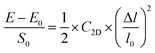
Density functional theory (DFT)26,27 calculations were performed for analysis of structural relaxation and electronic properties as implemented in the Quantum ESPRESSO software package.28 The generalized gradient approximation (GGA) based Perdew−Burke−Ernzerhof (PBE) functional29 was used for approximating the exchange–correlation term. The long-range dispersion correction was described by using the DFT-D3 method.30 A plane wave cutoff energy of 680 eV and the projector augmented-wave (PAW) pseudo-potential31 were used to treat the electron–ion core interaction. Brillouin zone sampling32 of 5 × 5 × 1 and 15 × 15 × 1 was performed for the structural optimization and density of states (DOS) computation of a 3 × 3 × 1 supercell of Oh-B2S2. In addition, spin-polarized DFT theory was adopted to deal with the unpaired electrons. A vacuum of 30 Å was considered along the z-direction to avoid inter-layer interaction. The lattice constant and the atomic position were relaxed with energy and Hellmann–Feynman force convergence criteria of 10−3 eV per atom and 0.01 eV Å−1. Phonon dispersion spectra of the monolayer were calculated using density functional perturbation theory (DFPT)33 with a grid of 6 × 6. Eqn (S1) and (S2) (ESI†) were implemented to determine the binding energy (Eb)12 and the cohesive energy (Ecoh)34 of the Oh-B2S2 monolayer. We have used deformation potential theory (DPT)12,35 to calculate the charge carrier mobility of the system, as stated in eqn (1a).12| |  | (1a) |
| |  | (1b) |
| |  | (1c) |
The parameters in eqn (1a)–(1c) are the charge of the electron (e), reduced Planck's constant  , Boltzmann's constant (kB), and temperature (T). m* and ma are the effective and average effective masses along the transport direction. C2D is the elastic modulus that can be calculated using eqn (1b), where E0 and E are the total energies of the crystal before and after deformation. S0 is the lattice volume and Δl and l0 are variations in the lattice constant and initial lattice constant. Eil is the deformation potential constant and can be obtained from eqn (1c), where ΔVi is the change in energy in the ith band under strain.
The computed adsorption energy (Eads) of the gas molecules over the Oh-B2S2 monolayer was given by eqn (2)23,36
| | | Eads = EOh-B2S2+gas − (Egas + EOh-B2S2) | (2) |
where
EOh-B2S2+gas,
Egas, and
EOh-B2S2 represent the energies of a fully relaxed gas molecule adsorbed Oh-B
2S
2 monolayer, an individual gas molecule, and an Oh-B
2S
2 monolayer, respectively. The Bader charge analysis
37 was performed to understand the charge transfer between the monolayer and the gas molecule. Furthermore, the calculation of the charge density difference (CDD) plot was done using
eqn (3)23 and visualized using the VESTA software.
38| | | ρcdd = ρOh-B2S2+gas − (ρgas + ρOh-B2S2) | (3) |
where
ρOh-B2S2+gas,
ρgas, and
ρOh-B2S2 represent the charge densities of the gas molecule adsorbed Oh-B
2S
2 monolayer, individual gas molecule, and Oh-B
2S
2 monolayer, respectively.
The thermal stability of the Oh-B2S2 monolayer and gas molecule adsorbed monolayer were investigated through ab initio molecular dynamics (AIMD) simulations using the CP2K code39 with the QUICKSTEP module. The DZVP-MOLOPT-SR-GTH basis set in conjunction with the Goedecker–Teter–Hutter (GTH) pseudopotential40,41 and a plane wave basis with a kinetic energy cutoff of 500 Ry were used to represent the Kohn–Sham orbitals and total electron density, respectively.
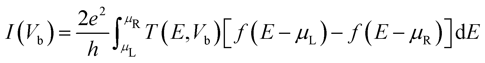
Furthermore, to evaluate the electron transport properties, we have used non-equilibrium Green's functional (NEGF) formalism42 implemented in the TranSIESTA software package.43 For the calculation, a 1 × 1 × 100 grid with the GGA-PBE functional at a cut-off of 500 Ry was used. The current through the central region was calculated based on the Landauer–Buttiker formula given as eqn (4).44,45
| |  | (4) |
Here,
T(
E,
Vb) is the transmission coefficient of electrons at energy
E and voltage
Vb,
f is the Fermi function, and
μR/L is the electrochemical potential of the right (R)/left (L) electrode.
3 Results and discussion
3.1 Structural feature analysis
Initially, the unit cell of Oh-B2S2, as depicted by the black dotted line in Fig. 1a, was optimized. The lattice constant of Oh-B2S2 was found to be a = b = 3.05 Å, and the B–S, B–B, and S–O bond lengths were 1.95, 1.72, and 1.47 Å, respectively, which are consistent with the h-B2S2 monolayer.12 The dynamic stability of the Oh-B2S2 monolayer was established by the absence of negative frequency in the phonon dispersion curve and projected density of phonon states, as shown in Fig. 1b and Fig. S1 (ESI†), respectively. The AIMD plot in Fig. 1c indicates thermal stability of the Oh-B2S2 structure at 300 K over 5 ps, and we have not observed any structural deformation during the simulations. Furthermore, the electronic properties of the monolayer were analyzed via electronic band structure and density of states plots. Fig. 1d shows that Oh-B2S2 is an indirect band gap semiconductor with a bandgap of 1.37 eV, whose valence band maximum (VBM) and conduction band minimum (CBM) are located at high symmetry k-points Γ and K, respectively. The presence of the oxygen atom significantly lowers the band gap of the Oh-B2S2 monolayer compared to that of h-B2S2.12 The band gap was calculated employing the HSE06 functional, as PBE-GGA underestimates the band gap value.46Fig. 1e displays the projected density of states (PDOS) of the monolayer, illustrating the overlapping of the s and p-orbitals of B-atoms, S-atoms, and O-atoms. To get insight into charge redistribution on the surface, we have calculated the charge density difference (CDD) plot, shown in Fig. 1f. Fig. 1f shows a charge accumulation region on the Oh-B2S2 monolayer, which is absent on the h-B2S2 monolayer [Fig. S2(a); ESI†]. This small surface charge density may be responsible for the negligible adsorption potential of the h-B2S2 monolayer, as shown in Fig. S2(b) of the ESI.† Besides, we have carried out electron localization function (ELF) analysis to examine the bonding characteristics between the sulfur (S) and oxygen (O) atoms, as depicted in Fig. S3 of the ESI.† ELF = 1.0 (red color) indicates complete localization of electrons, while ELF = 0.5 (green color) indicates delocalization.47 In Fig. S3 (ESI†), the electron localization between S and O atoms is indicated by the ELF within the range of 0.75 to 0.85.
 |
| | Fig. 1 (a) Top and side view of Oh-B2S2 monolayer (the black dotted line shows the unit cell); (b) phonon dispersion spectrum plot; (c) AIMD plot at 300 K; (d) electronic band structure (HSE06 functional); (e) projected density of states (PDOS); (f) charge density difference (CDD) plot (blue and pink colors indicate the charge accumulation and depletion regions, respectively) of the oxygen-functionalized B2S2 (Oh-B2S2) monolayer. Green, yellow, and red balls indicate the boron, sulfur, and oxygen atoms. | |
In addition, to understand the experimental feasibility, we have calculated the Eb and Ecoh of the Oh-B2S2 monolayer. The computed Eb value was determined to be −5.28 eV, which is greater as compared to the binding energy of the OT-B2S2 monolayer (Table S1; ESI†). Furthermore, the Ecoh of the Oh-B2S2 monolayer was found to be 5.54 eV per atom, slightly lower than that of the h-B2S2 monolayer.12 However, this cohesive energy is higher than those of other experimentally realized 2D materials such as blue phosphorene (3.48 eV per atom),48 silicene (4.57 eV per atom),49etc. Carrier mobility (electrons/holes) of semiconductors is a crucial parameter that impacts the efficiency of devices, including energy consumption and electrical performance.50 Since Oh-B2S2 is a p-type semiconductor with holes as the majority carrier, we have determined the mobility of both holes and electrons. The carrier mobilities of Oh-B2S2 were calculated to be 790 × 102 cm2 V−1 s−1 for electrons and 32 × 102 cm2 V−1 s−1 for holes (Fig. S4; ESI†), surpassing those of the MoS2 monolayer.51,52 The high carrier mobility of the Oh-B2S2 monolayer can be explained using the equation  .53 It has been noted that the carrier mobility of a system varies inversely with the effective masses of electrons and holes. Upon comparing the effective masses of electrons and holes in MoS2 and Oh-B2S2 from Table S2 (ESI†), we have found that these values are lower for Oh-B2S2, resulting in higher carrier mobility.53 Furthermore, the high elastic modulus and deformation potential ratio are essential parameters influencing the high carrier mobility of the Oh-B2S2 monolayer (Table S2, ESI†).54 For reference, we have also calculated the electron and hole carrier mobilities of MoS2, which were found to be 280 and 161 cm2 V−1 s−1, respectively.20,50,55 Fig. S4 (ESI†) shows the deformation potential plot for electron and hole mobilities and the elastic modulus plot of MoS2.
3.2 Adsorption properties of the Oh-B2S2 monolayer
Prior to the investigation, the sensing properties of the Oh-B2S2 monolayer were assessed by studying the adsorption of toxic gases CO, NO, CO2, NO2, N2O, and SO2. These gaseous pollutants were introduced on the Oh-B2S2 monolayer at various adsorption orientations at a 3 Å distance. The adsorption energies of the gas molecules with different orientations are shown in Fig. 2a and Fig. S5 (ESI†). Fig. 2b depicts the optimized structure of the energetically most favored adsorption configuration, in which the molecules preferentially remain parallel to the surface. The adsorption distance (d) between the gas molecule and the surface was further confirmed by the potential energy curves (PECs) shown in Fig. S6 of the ESI.† The adsorption energy can be used to quantitatively evaluate the adsorption strength between the gas molecules and the monolayer. All negative values of adsorption energies for each gas molecule indicate that adsorption was an exothermic process with thermodynamic stability, which is favorable for the sensing applications.56 The most favorable adsorption sites were identified by the highest adsorption energies from an energetically favorable viewpoint, as shown in Table 1. The positive charge transfer (CT) values (Table 1) indicate that the gas molecules behave as donors.
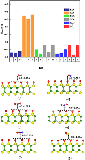 |
| | Fig. 2 (a) Adsorption energies (Eads) of the gas molecules at different orientations. (b)–(g) Top view of preferable optimized geometries of the Oh-B2S2 monolayer after adsorption of CO, NO, CO2, NO2, N2O, and SO2, respectively, on their most favorable sites. Yellow, green, red, blue, and grey balls represent S, B, O, N, and C atoms. AD = adsorption distance. | |
Table 1 Computed adsorption energies (Eads), charge transfer values (Qe), adsorption distances (d), bond lengths (l), and bond angles (Θ) of the gas molecules before and after adsorption on the Oh-B2S2 monolayer
| Gas molecule |
E
ads (eV) |
Q
e
|
d (Å) |
Before adsorption |
After adsorption |
|
l (Å) |
Θ (°) |
l (Å) |
Θ (°) |
| CO |
−0.07 |
0.006 |
3.03 |
1.13 |
— |
1.13 |
— |
| NO |
−0.56 |
0.340 |
2.45 |
1.16 |
— |
1.13 |
— |
| CO2 |
−0.10 |
0.004 |
2.87 |
1.17 |
179.89 |
1.17 |
179.89 |
| NO2 |
−0.16 |
0.133 |
2.67 |
1.21 |
133.41 |
1.20 |
136.81 |
| N2O |
−0.10 |
0.009 |
3.00 |
1.19/1.15 |
179.98 |
1.19/1.14 |
179.86 |
| SO2 |
−0.11 |
0.009 |
2.85 |
1.45 |
119.42 |
1.45 |
118.99 |
Table 1 reveals that the NO molecule interacts with the monolayer with considerable binding energy47 and charge transfer value among all other molecules. Furthermore, it was worth noting that the adsorption distance of the NO gas molecule exhibits a relatively small value of 2.45 Å compared to the other gases. Additionally, the O–N bond length experienced a reduction of 0.03 Å relative to the length of the isolated NO molecule. The adsorption energy of NO in the Oh-B2S2 monolayer is higher than those in many previously reported materials such as graphene57 (0.02 eV), WS258 (−0.25 eV), silicene59 (−0.35 eV), MoS260 (−0.19 eV), phosphorene61 (−0.32 eV), etc. Besides, as the gas sensing mechanism is essentially dependent on the charge transfer phenomenon, Table 1 indicates that the CT value of NO2 is sufficient enough to influence the properties of the Oh-B2S2 monolayer.61 This CT value of NO2 for the Oh-B2S2 monolayer is greater than those of graphene57 (−0.09e) and MoS262 (0.04e) monolayers. In addition, the adsorption of NO2 gas molecules onto an Oh-B2S2 monolayer occurs at an interfacial distance of 2.67 Å. However, the remaining four gas molecules, CO, CO2, N2O, and SO2, interact weakly due to their longer adsorption distances, resulting in small CT values.
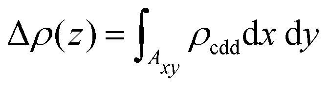
The phenomenon of charge redistribution is visually depicted in Fig. 3via a charge density difference (CDD) plot. CDD qualitatively reveals the regions of charge accumulation (blue color) and depletion (pink color) in the entire system, providing insight into the charge transfer between the gas molecules and the surface. Charge donation to the surface occurs for all six gas molecules (CO, NO, CO2, NO2, N2O, and SO2), as charge accumulates on them. As depicted in Fig. 3(a), (c), (e) and (f), negligible charge redistributions were observed between molecule–monolayer systems, resulting in relatively weak binding strength. However, in the case of NO and NO2 adsorbed systems (Fig. 3(b) and (d)), there is a noticeable redistribution of charge within the molecule and a significant increase in charge transfer between the molecule and the Oh-B2S2 monolayers. This observation highlights the greater sensitivity of the Oh-B2S2 monolayer towards NO and NO2 molecules. In order to gain a more thorough understanding of the charge redistribution within the system, we have computed the plane-averaged charge density difference Δρ(z) over the xy-plane according to eqn (5)
| |  | (5) |
Here,
Axy denotes the surface area of the supercell, and the function
ρcdd is defined by
eqn (3).
Fig. 4(b) and (d) indicate the presence of a notable region of charge accumulation on the surface, and the curves' amplitude is high compared to
Fig. 4(a), (c), (e) and (f). This finding aligns with our charge density difference and charge transfer value studies (
Fig. 3).
 |
| | Fig. 3 Charge density difference (CDD) plots of (a) CO, (b) NO, (c) CO2, (d) NO2, (e) N2O, and (f) SO2 adsorbed Oh-B2S2 monolayers, respectively. Pink and blue colors depict the charge depletion and accumulation regions, respectively, at an iso-surface value of 0.003 e Bohr−3. | |
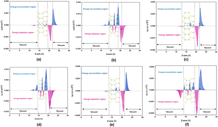 |
| | Fig. 4 Plane-average charge density difference (CDD) plots of (a) CO, (b) NO, (c) CO2, (d) NO2, (e) N2O, and (f) SO2 adsorbed Oh-B2S2 monolayers, respectively. Blue and pink colors depict the charge accumulation and depletion regions, respectively. | |
3.2.1 Electronic property analysis.
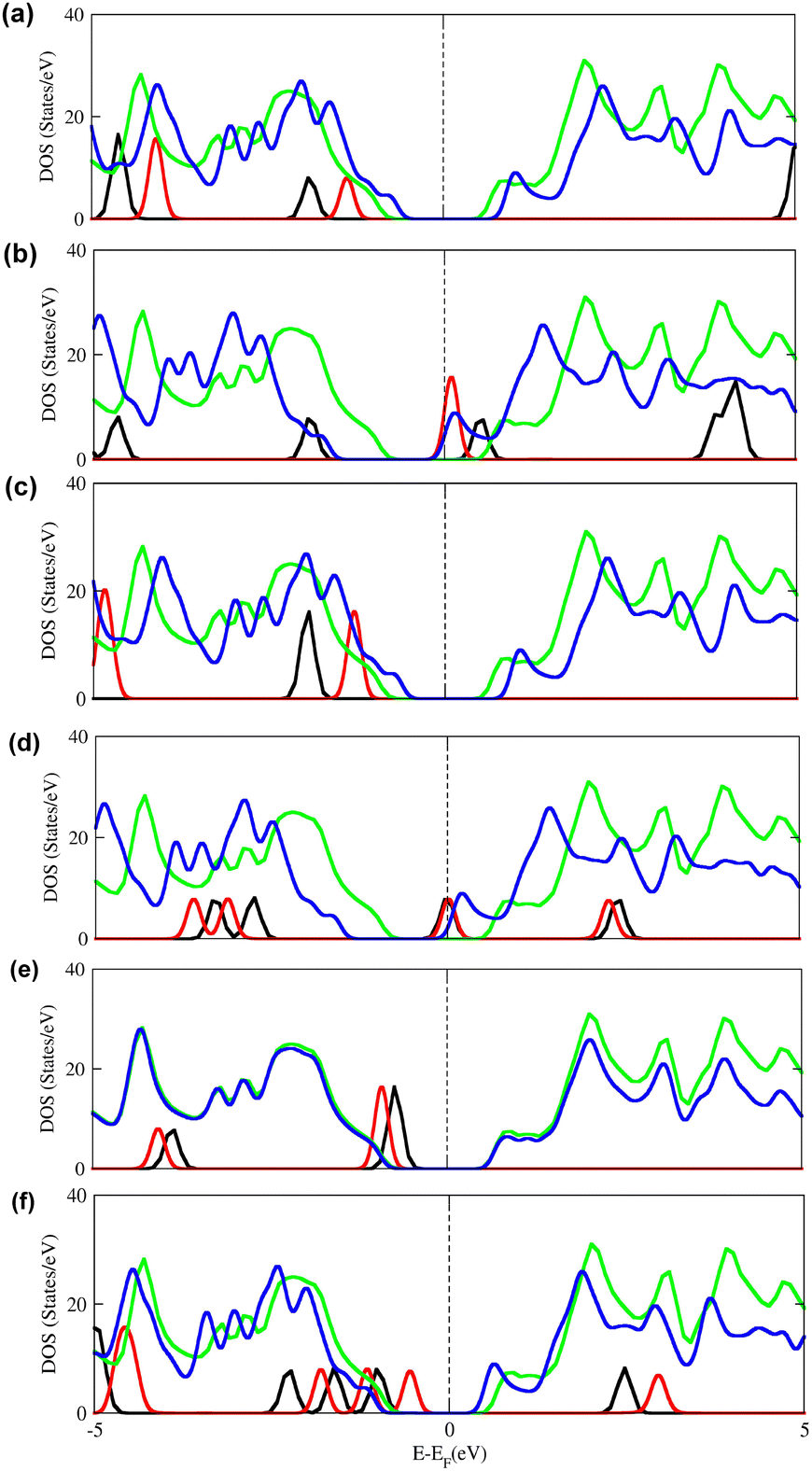
Furthermore, to obtain a reliable depiction of alterations in the electronic structure that occur subsequent to gas molecule adsorption, we have calculated the density of states (DOS) plots before and after the adsorption of each molecule, as shown in Fig. 5. The overlap of atomic orbital peaks on the DOS curves reveals the hybridization between atomic orbitals and, thus, the extent of interaction between atoms. Meanwhile, this parameter will influence the conductivity change of the system. The total density of states (TDOS) curve rises and declines around the Fermi level, influencing the conductivity change of the system. Fig. 5(b) and (d) illustrates the existence of novel peaks at the Fermi-level (EF) in the Oh-B2S2 monolayer upon adsorption of NO and NO2. The electronic structure modification through adsorption and charge transfer impacts the conductivity of the Oh-B2S2 monolayer, which can provide a response signal for the potentially hazardous molecules, as evidenced by prior studies.23 In contrast, for other gas molecules such as CO, CO2, N2O, and SO2, no such interactions are present at the Fermi level or close to the Fermi level. The above observation can be explained by the relatively low adsorption energies and negligible CT values. This finding suggests that the adsorption of these gases causes an insignificant influence on the electronic behaviour of the Oh-B2S2 monolayer, as displayed in Fig. 5(a), (c), (e) and (f).
 |
| | Fig. 5 Density of states (DOS) plots of (a) CO, (b) NO, (c) CO2, (d) NO2, (e) N2O, and (f) SO2 before and after adsorption upon Oh-B2S2 nanosheets. Green and blue colours indicate the DOS of Oh-B2S2 before and after gas adsorption, and black and red colours indicate the DOS of isolated and adsorbed gas molecules. The black dotted line represents the Fermi-level (EF). | |
Based on the calculations carried out until now, it was observed that the Oh-B2S2 monolayer exhibits remarkable charge transfer values and alteration of its electronic properties only when interacting with NO and NO2 molecules. A possible reason for considerable CT and electronic property modulation is the presence of unpaired electrons on NO and NO2. Hence, spin-polarized density functional theory was employed to examine the impact of an unpaired electron. Table S3 of the ESI† presents the adsorption energies, charge transfer values, and adsorption distances, which show minor variations from the density functional theory calculation results. The spin-polarized density of states (SPDOS) depicted in Fig. S7 of the ESI† demonstrate the existence of orbital overlap at the Fermi level, which profoundly affects the electronic properties of the Oh-B2S2 monolayer. Furthermore, to check if the 3 × 3 supercell is sufficient to describe the adsorption properties of the material towards NO and NO2, we have extended our calculation to 4 × 4 and 5 × 5 supercells, and results are shown in Table S4 of the ESI.† From Table S4 (ESI†), it can be seen that there is a very minimal difference in the Eads and CT values as the size of the supercell increases. Therefore, we can conclude that the sensing potential of the Oh-B2S2 monolayer can be well explained by the 3 × 3 supercell.
3.3 Selectivity and temperature dependence of NO and NO2 adsorption–desorption dynamics on the Oh-B2S2 monolayer
The term selectivity refers to the potential of gas sensors to distinguish particular gas molecules from various gases.23,36 Therefore, to investigate the Oh-B2S2 monolayer for its potential application as a practical gas sensor, we have determined the impact of prominent environmental gases along with some other gases (such as O2, N2, H2, H2O, O3, and CH4)63 on its surface. The H2O molecule was incorporated into our calculation to determine humidity.64 Fig. S8 of the ESI† illustrates the optimized geometries associated with the most favorable adsorption configuration for each gas molecule. All stable adsorption has a parallel configuration with a minimum distance between 2.85 and 2.99 Å. The data associated with the adsorption of gas molecules on the Oh-B2S2 monolayer are displayed in Table S5 of the ESI.† The results reveal that the interaction strength and CT value pertaining to the NO and NO2 molecules on Oh-B2S2 are higher compared to those of the other gases. The Eads for NO and NO2 were −0.56 and −0.16 eV, respectively, and the corresponding CT values were 0.34 and 0.13e. In contrast, the Eads values for the other atmospheric gases range from −0.03 to −0.12 eV, and the CT values range from 0.004 to 0.08e (Fig. S9; ESI†). This demonstrated the considerable preference for NO and NO2 gases with high selectivity in the presence of other environmental gases.
The working features of a sensor can undergo significant changes when exposed to finite temperatures. Hence, it is crucial to ascertain the fundamental dynamics, i.e., the adsorption–desorption behavior of the sensor at various temperatures, before implementation.65 The underlying dynamic behavior of NO and NO2 on the Oh-B2S2 monolayer was studied using AIMD simulations at T = 300 K, 350 K, and 400 K for 10 picoseconds (ps) based on the constant particle number–volume–temperature (NVT) canonical ensemble with the Nosé thermostat.66Fig. 6 presents the AIMD plots alongside the atomic structure of the system at various temperatures after simulation. The findings of our AIMD simulations demonstrated the room temperature stability of the NO-adsorbed Oh-B2S2 monolayer [Fig. 6a], where variations in energy over time remain stable around a given constant. However, an increase in temperature to 350 K leads to changes in the adsorption structure. Consequently, the molecule begins to desorb from the surface, demonstrating a time scale in the femtosecond (fs) range throughout the simulation. The atomic structure of the NO2-adsorbed Oh-B2S2 monolayer attains equilibrium at different temperatures, as depicted in Fig. 6(b). The observed configuration indicates that during the simulations, the NO2 molecule remains close to the surface up to a temperature of 350 K. Nevertheless, as the temperature increases to 400 K, the NO2 molecule was observed to undergo desorption from the surface within a time frame of 0.2 ps. In summary, the AIMD results indicate that the desorption temperatures for NO and NO2 over the Oh-B2S2 monolayer were between 300–350 K and 350–400 K, respectively. Therefore, it may be inferred that the Oh-B2S2 monolayer demonstrates favorable gas sensing capabilities for NO and NO2 molecules at ambient temperature. The room temperature functioning of the Oh-B2S2 nanosensor towards NO and NO2 eliminates the requirement for a heat source in high-temperature applications, streamlining device production and lowering operating costs.67
 |
| | Fig. 6
Ab initio molecular dynamics (AIMD) simulation plots of (a) NO and (b) NO2 adsorbed Oh-B2S2 monolayers for 10 ps at T = 300 K, 350 K, and 400 K with their final geometries. | |
Furthermore, we have determined the desorption time (τ) of the gas molecule at a temperature of 300 K. It refers to the minimum amount of time needed for a sensor to remove the adsorbed gases from its surface. The value of τ can be theoretically determined by using the transition state theory and van't-Hoff–Arrhenius equation36,68 as follows:
| |  | (6) |
Here
A is the attempt frequency (10
12 s
−1, for visible light),
T is the temperature, and
kB is the Boltzmann constant.
69 The
Eads examined at a temperature of 300 K corresponds to the adsorption configuration of NO and NO
2 after the simulations for 10 ps. The corresponding energies for NO and NO
2 are −0.54 and −0.13 eV. Thus, the estimated desorption times for NO and NO
2 were 0.80 milliseconds (ms) and 0.15 nanoseconds (ns) under visible light irradiation and at ambient temperature (300 K).
3.4 Work function of the sensor
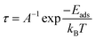
The expression for the work function (ϕ) of a 2D material can be represented as, ϕ = Evac − EF.70 Here, EF is the energy associated with the Fermi level of the material from which the electron is extracted and Evac is the energy required to overcome the surface dipole barrier, which approaches a constant at a significant distance from the surface.70 We have estimated the work functions of the Oh-B2S2 monolayer before and after NO and NO2 adsorption. An inherent polarisation electric field exists owing to the asymmetry of the Oh-B2S2 monolayer.71 Hence, a dipole correction was implemented while calculating the average electrostatic potential plot, as depicted in Fig. S10 of the ESI.† Fig. S10 (ESI†) shows that the electrostatic potential difference (U) decreases after the adsorption of gas molecules (UOh-B2S2: 4.19 eV > UOh-B2S2+NO2: 3.13 eV > UOh-B2S2+NO: 2.34 eV). This phenomenon can be ascribed to the intrinsic dipole moment of the gas molecules and the charge transfer between the two interfaces. The work functions of the Oh-B2S2 monolayer, Oh-B2S2 + NO, and Oh-B2S2 +NO2 were determined to be 6.91, 4.74, and 5.82 eV, respectively. As the gas molecules act as donors, the work function of the monolayer decreases after adsorption. Fig. 7 illustrates the pictorial depiction of alterations in the work function of the Oh-B2S2 monolayer with adsorbed NO and NO2 compared to the pristine system. Experimentally, the change in work function due to gas adsorption is estimated via a scanning Kelvin probe, which has led to the realization of gas sensors that rely on work function measurements.69
 |
| | Fig. 7 Pictorial depiction of alterations in the work function of the Oh-B2S2 nanosheets with adsorbed NO and NO2 compared to the pristine system. | |
3.5
I–V characteristic plots
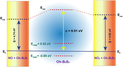
It is essential to explore the possibility of the Oh-B2S2 monolayer to be used as a gas sensing tool from a device point of view.23,72 Despite some gas molecules altering the electronic structure around the Fermi level, the charge transfer generated by the adsorption of the gas molecules on the monolayer can produce varied sensitivities for resistivity measurements.47,72 Therefore, the efficacy of the Oh-B2S2 monolayer as a potential gas sensor can be specifically assessed by applying the non-equilibrium Green's function (NEGF) method23,47 to calculate the transmission properties and current–voltage (I–V) characteristics. Two semi-infinite electrodes were considered during the investigation, which are the periodic extensions of the pristine monolayer termed “pseudo-electrodes”. A similar simplified device model has been extensively used in previous publications.72–74 Two transport models were computed for the direction of the current flow, namely the x-direction (zigzag) and the y-direction (armchair), due to the structural anisotropy of the Oh-B2S2 monolayer (Fig. 8). Because the zero-bias transmission was higher along the zigzag direction (Fig. 9a), we have considered the transport along that direction. A transmission gap around the Fermi level was observed in both directions due to the semiconductor nature of the material. To analyze the qualitative sensitivity of the Oh-B2S2 monolayer towards NO and NO2 gases, we have simulated the current–voltage relationships before and after gas adsorption using a model as shown in Fig. 8b. The I–V characteristic plots of the bare Oh-B2S2 and gas-adsorbed Oh-B2S2 monolayers are shown in Fig. 9b. From the I–V plots, it can be seen that there is no current flow up to 1.0 bias voltage in all cases (bare Oh-B2S2 surface and gas-adsorbed Oh-B2S2). Introducing a bias voltage causes the shifting of the left electrodes Fermi level in accordance with the right electrode. Thus, the current begins to flow only when the left electrode's VBM crosses over into the right electrode's CBM.75Fig. 9b demonstrates that the current through a device based on the Oh-B2S2 monolayer decreases when the device is exposed to gas molecules NO and NO2. The presence of an unpaired electron in the NO and NO2 molecules induces the localization of the wavefunction and may lead to pronounced back-scattering and the subsequent suppression of conductive pathways.72,75,76 At biases of 1.2 and 1.4 V, the NO-adsorbed Oh-B2S2 monolayer experiences a reduction in current flow to 45% and 81%, respectively. This outcome suggests that the material exhibits a favorable sensitivity towards NO in 1.2 and 1.4 V bias voltage regions. Nevertheless, with increased voltage, there was a major decrease in the magnitude of current flow within the range of 10−15 to 10−16 nA. Moreover, it has been identified that the sensitivity towards NO2 reaches its maximum at bias voltage 2 V, resulting in the corresponding decrease in the current by 91%. In contrast, the I–V characteristic plots of several environmental gases (including O2, N2, and H2) and toxic gases (such as CO, CO2, N2O, and SO2) are almost comparable to that of the Oh-B2S2 monolayer. This observation reveals the weak bonding characteristics between the gas molecules and the substrate, which we have previously discussed.
 |
| | Fig. 8 Schematic representation of the electron transport model of the Oh-B2S2 monolayer along the (a) armchair direction and (b) zigzag direction. The device setup consists of a left electrode, a right electrode, and a central scattering region. | |
 |
| | Fig. 9 (a) Zero bias transmission spectral T(E) plots along zigzag and armchair directions, (b) I–V characteristic plots of the Oh-B2S2 monolayer and gas-adsorbed Oh-B2S2 nanosheets (gases: CO, NO, CO2, NO2, N2O, SO2, H2, N2, and O2). | |
Furthermore, it was noted from the individual plots (Fig. 9b) that there is no monotonic increase in the current with respect to the voltage. In the case of bare Oh-B2S2, the current increases from 0.74 to 11 nA as the bias voltage is raised from 1.2 to 2.0 V. However, a minor reduction in the current was noticed at a bias voltage of 1.4 V. For NO-adsorbed Oh-B2S2, a marginal rise in current was observed at 1.2 V, followed by a sharp decline in current as the voltage is increased from 1.4 to 2.0 V. Similarly, the NO2-adsorbed Oh-B2S2 monolayer causes a rise in current to 2.72 nA at 1.6 V, which further reduces to 0.94 nA at 2.0 V. The decrease in the current with an increase in the voltage can be explained by the negative differential resistance (NDR) phenomenon.77,78 Such NDR behaviors in para-SiC3,79 boron–phosphorus,47 and defect-borophene monolayers80 have been reported recently. The origin of the NDR phenomenon of Oh-B2S2 and gas-adsorbed Oh-B2S2 can be explained by transmission spectra [T(E)] at different biases.81,82 In the case of Oh-B2S2, an NDR phenomenon was observed at 1.4 V bias voltage. Upon comparing the T(E) at bias voltages 1.2, 1.4, and 1.6 V, the amplitude of the transmission peak at 1.4 V was comparatively small within the bias window (Fig. S11, ESI†), and hence the current drops at that bias. Similarly, for NO and NO2 adsorbed Oh-B2S2 monolayers, the transmission spectra are shown in Fig. S12 and S13 of the ESI.† The low magnitude of the transmission peak was observed in the bias window from 1.4 V (for NO-adsorbed Oh-B2S2) and after 1.6 V (for NO2-adsorbed Oh-B2S2), leading to the suppression of current. Transmission spectra are generated as a result of the conductance channels that are accessible within different energy bands. The decrease in conductance channels at certain biases results in the corresponding decrease in the flow of electrical current,75 which is consistent with the previously proposed NDR mechanisms.81
3.6 Comparative analysis of the Oh-B2S2 monolayer and MoS2 monolayer towards NO and NO2 detection
Low carrier mobility in the MoS2 monolayer demands high bias voltage for resistance measurement.63 Similar to MoS2, but with a B2 ion pair in place of the Mo ions, we believe that the B2S2 monolayer can overcome the shortcomings of the MoS2 monolayer. It was determined that the Oh-B2S2 monolayer, which has been functionalized with oxygen atoms, exhibits charge carrier mobilities of 790 × 102 cm2 V−1 s−1 and 32 × 102 cm2 V−1 s−1 for electrons and holes. This high mobility is attributed to the fast operation of the device. On the contrary, the MoS2 monolayer demonstrates an electron mobility of 280 cm2 V−1 s−1 and a hole mobility of 161 cm2 V−1 s−1. Meanwhile, a comparison was made between the Eads and CT values of NO and NO2 adsorption on Oh-B2S2 and MoS2. Although the Eads of NO2 was found to be slightly higher in MoS2, the gas sensing mechanism primarily relies on the charge transfer value. Table 2 reveals that Oh-B2S2 monolyer exhibited a relatively higher adsorption potential towards NO and NO2 compared to the MoS2 monolayer.60,62,83,84
Table 2 Theoretical prediction of Eads and CT values of NO and NO2-adsorption on MoS2 and Oh-B2S2 (vdW: van der Waals correction)
| Material |
Gas |
E
ads (eV) |
CT (e) |
Methods |
Ref. |
| MoS2 |
NO |
−0.03 |
0.02 |
GGA-PBE |
83
|
| −0.19 |
— |
GGA-PBE |
60
|
| −0.17 |
— |
GGA-PBE (vdW) |
84
|
| NO2 |
−0.01 |
0.11 |
GGA-PBE |
83
|
| −0.20 |
0.04 |
GGA-PBE (vdW) |
62
|
| −0.17 |
−0.03 |
GGA-PBE (vdW) |
84
|
| Oh-B2S2 |
NO |
−0.56 |
0.34 |
GGA-PBE (vdW) |
This work |
| NO2 |
−0.16 |
0.13 |
GGA-PBE (vdW) |
This work |
4 Conclusions
In a nutshell, we have investigated the structure, stability, and electronic properties of an oxygen-functionalized B2S2 (Oh-B2S2) monolayer via density functional theory and ab initio molecular dynamics (AIMD) simulations. The monolayer was observed to be stable and ideal for experimental fabrication with an indirect band gap of 1.37 eV. Our findings show that the Oh-B2S2 monolayer has high sensitivity and selectivity for NO and NO2 gas molecules, even in the presence of common ambient gases like O2, N2, H2, H2O, O3, and CH4 as well as harmful pollutants, including CO, CO2, N2O, and SO2. To further confirm the adsorption behaviors of Oh-B2S2 towards gaseous molecules, charge transfer, work function, and electronic property studies were carried out. The presence and absence of gas molecules (functioning as ON and OFF states) are further demonstrated by the current–voltage (I–V) characteristic plot for device application. Our results unambiguously show negative differential resistance (NDR) in the presence of NO and NO2 molecules after 1.2 and 1.6 V bias voltages, respectively. We hope our findings presented in this study may help to explain the sensing properties of the material and subsequently aid in the development of boron-based functionalized nanosensors for the detection of hazardous gases.
Conflicts of interest
The authors declare no conflict of interest.
Acknowledgements
The authors acknowledge the Supercomputing facility ‘PARAM-Ishan’ and National Supercomputing Mission (NSM) for providing computing resources of ‘PARAM Kamrupa’ at IIT Guwahati, which is implemented by C-DAC and supported by the Ministry of Electronics and Information Technology (MeitY) and the Department of Science and Technology (DST), Government of India. UN acknowledges the support from the Department of Science and Technology (DST), India, for an INSPIRE Fellowship (No. DST/INSPIRE Fellowship/2018/IF180745).
Notes and references
- S. Srivastava, P. Pal, D. K. Sharma, S. Kumar, T. Senguttuvan and B. K. Gupta, ACS Mater., 2022, 2, 356–366 Search PubMed.
- I. Manisalidis, E. Stavropoulou, A. Stavropoulos and E. Bezirtzoglou, Front. Public Health, 2020, 8, 14–26 Search PubMed.
- S. C. Anenberg, J. Miller, R. Minjares, L. Du, D. K. Henze, F. Lacey, C. S. Malley, L. Emberson, V. Franco and Z. Klimont,
et al.
, Nature, 2017, 545, 467–471 Search PubMed.
- A. K. Singh, C.-C. Yen, C.-F. Wen, R.-H. Horng and D.-S. Wuu, ACS Appl. Electron. Mater., 2023, 2574–2582 Search PubMed.
- L. Yu and F. Li, Phys. Chem. Chem. Phys., 2022, 24, 9842–9847 Search PubMed.
- D. Qin, T. Chen, L. Xie, N. Yang, C. Luo and G. Zhou, Phys. Chem. Chem. Phys., 2023, 25, 29315–29326 Search PubMed.
- G. Fiori, F. Bonaccorso, G. Iannaccone, T. Palacios, D. Neumaier, A. Seabaugh, S. K. Banerjee and L. Colombo, Nat. Nanotechnol., 2014, 9, 768–779 Search PubMed.
- R. Li, Y. Cheng and W. Huang, Small, 2018, 14, 1802091–1802101 Search PubMed.
- B. Babariya, D. Raval, S. K. Gupta and P. Gajjar, Phys. Chem. Chem. Phys., 2022, 24, 15292–15304 Search PubMed.
- T. Pham, G. Li, E. Bekyarova, M. E. Itkis and A. Mulchandani, ACS Nano, 2019, 13, 3196–3205 Search PubMed.
- B. Cho, M. G. Hahm, M. Choi, J. Yoon, A. R. Kim, Y.-J. Lee, S.-G. Park, J.-D. Kwon, C. S. Kim and M. Song,
et al.
, Sci. Rep., 2015, 5, 8052–8057 Search PubMed.
- C. Tang, F. Ma, C. Zhang, Y. Jiao, S. K. Matta, K. Ostrikov and A. Du, J. Mater. Chem. C, 2019, 7, 1651–1658 Search PubMed.
- D. Fan, S. Lu, C. Chen, M. Jiang, X. Li and X. Hu, Appl. Phys. Lett., 2020, 117, 013103–013107 Search PubMed.
- S. Demirci, N. Avazl, E. Durgun and S. Cahangirov, Phys. Rev. B, 2017, 95, 115409–115416 Search PubMed.
- H. Kusaka, R. Ishibiki, M. Toyoda, T. Fujita, T. Tokunaga, A. Yamamoto, M. Miyakawa, K. Matsushita, K. Miyazaki and L. Li,
et al.
, J. Mater. Chem. A, 2021, 9, 24631–24640 Search PubMed.
- P. Mishra, D. Singh, Y. Sonvane and R. Ahuja, J. Appl. Phys., 2020, 127, 184305–184314 Search PubMed.
- P. Mishra, D. Singh, Y. Sonvane and R. Ahuja, Sustainable Energy Fuels, 2020, 4, 2363–2369 Search PubMed.
- B. Mortazavi and T. Rabczuk, Energies, 2018, 11, 1573–1583 Search PubMed.
- Y. Zhang, M. Zhou, M. Yang, J. Yu, W. Li, X. Li and S. Feng, ACS Appl. Mater. Interfaces, 2022, 14, 32330–32340 Search PubMed.
- B. Radisavljevic, A. Radenovic, J. Brivio, V. Giacometti and A. Kis, Nat. Nanotechnol., 2011, 6, 147–150 Search PubMed.
- H. Zhao, J. Ye, W. Song, D. Zhao, M. Kang, H. Shen and Z. Li, ACS Appl. Mater. Interfaces, 2020, 12, 6991–7000 Search PubMed.
- A. Ostadhossein, J. Guo, F. Simeski and M. Ihme, Commun. Chem., 2019, 2, 95–105 Search PubMed.
- S. Ma, D. Yuan, Z. Jiao, T. Wang and X. Dai, J. Phys. Chem. C, 2017, 121, 24077–24084 Search PubMed.
- Y. Guo and W. Guo, J. Phys. Chem. C, 2015, 119, 873–878 Search PubMed.
- S. E. Zaki, M. A. Basyooni, M. Shaban, M. Rabia, Y. R. Eker, G. F. Attia, M. Yilmaz and A. M. Ahmed, Sens. Actuators, A, 2019, 294, 17–24 Search PubMed.
- P. Hohenberg and W. Kohn, Phys. Rev. B: Condens. Matter Mater. Phys., 1964, 136, 864–871 Search PubMed.
- K. Burke, J. Chem. Phys., 2012, 136, 150901–150909 Search PubMed.
- P. Giannozzi, S. Baroni, N. Bonini, M. Calandra, R. Car, C. Cavazzoni, D. Ceresoli, G. L. Chiarotti, M. Cococcioni and I. Dabo,
et al.
, J. Phys.: Condens. Matter, 2009, 21, 395502 Search PubMed.
- J. P. Perdew, K. Burke and M. Ernzerhof, Phys. Rev. Lett., 1996, 77, 3865–3868 Search PubMed.
- J. Moellmann and S. Grimme, J. Phys. Chem. C, 2014, 118, 7615–7621 Search PubMed.
- P. E. Blöchl, Phys. Rev. B: Condens. Matter Mater. Phys., 1994, 50, 17953–19979 Search PubMed.
- H. J. Monkhorst and J. D. Pack, Phys. Rev. B: Condens. Matter Mater. Phys., 1976, 13, 5188–5191 Search PubMed.
- S. Baroni, S. De Gironcoli, A. Dal Corso and P. Giannozzi, Rev. Mod. Phys., 2001, 73, 515–562 Search PubMed.
- H. Shin, S. Kang, J. Koo, H. Lee, J. Kim and Y. Kwon, J. Chem. Phys., 2014, 140, 114702–114707 Search PubMed.
- J. Xie, Z. Zhang, D. Yang, D. Xue and M. Si, J. Phys. Chem. Lett., 2014, 5, 4073–4077 Search PubMed.
- U. Nath and M. Sarma, J. Phys. Chem. A, 2023, 127, 1112–1123 Search PubMed.
- E. Sanville, S. D. Kenny, R. Smith and G. Henkelman, J. Comput. Chem., 2007, 28, 899–908 Search PubMed.
- K. Momma and F. Izumi, J. Appl. Crystallogr., 2008, 41, 653–658 Search PubMed.
- T. D. Kuhne, M. Iannuzzi, M. Del Ben, V. V. Rybkin, P. Seewald, F. Stein, T. Laino, R. Z. Khaliullin, O. Schutt and F. Schiffmann,
et al.
, J. Chem. Phys., 2020, 152, 194103–194149 Search PubMed.
- S. Goedecker, M. Teter and J. Hutter, Phys. Rev. B: Condens. Matter Mater. Phys., 1996, 54, 1703–1710 Search PubMed.
- J. VandeVondele and J. Hutter, J. Chem. Phys., 2007, 127, 114105–114113 Search PubMed.
- V.-N. Do, Adv. Nat. Sci.: Nanosci. Nanotechnol., 2014, 5, 033001–033021 Search PubMed.
- N. Papior, N. Lorente, T. Frederiksen, A. Garca and M. Brandbyge, Comput. Phys. Commun., 2017, 212, 8–24 Search PubMed.
- P. Ou, P. Song, X. Liu and J. Song, Adv. Theory Simul., 2019, 2, 1800103–1800111 Search PubMed.
- E.-A. Haidar, S. A. Tawfik, C. Stampfl, K. Hirao, K. Yoshizawa, S. H. El-Demerdash, T. Nakajima and A. M. El-Nahas, Phys. Chem. Chem. Phys., 2019, 21, 17859–17867 Search PubMed.
- Á. Morales-Garca, R. Valero and F. Illas, J. Phys. Chem. C, 2017, 121, 18862–18866 Search PubMed.
- S. Thomas, V. Kumar, D. R. Roy and M. A. Zaeem, ACS Appl. Nano Mater., 2020, 3, 10073–10081 Search PubMed.
- C. Wang, Y. You and J.-H. Choi, Mater. Res. Express, 2019, 7, 015005–015012 Search PubMed.
- B. Peng, H. Zhang, H. Shao, Y. Xu, R. Zhang and H. Zhu, J. Mater. Chem. C, 2016, 4, 3592–3598 Search PubMed.
- L. Ji, J. Shi, Z. Zhang, J. Wang, J. Zhang, C. Tao and H. Cao, J. Chem. Phys., 2018, 148, 014704–014711 Search PubMed.
- F. Guo, Z. Liu, M. Zhu and Y. Zheng, Phys. Chem. Chem. Phys., 2019, 21, 22879–22887 Search PubMed.
- Z. Jin, X. Li, J. T. Mullen and K. W. Kim, Phys. Rev. B: Condens. Matter Mater. Phys., 2014, 90, 045422–045428 Search PubMed.
- S. H. Mir, V. K. Yadav and J. K. Singh, ACS Omega, 2020, 5, 14203–14211 Search PubMed.
- J. Xiao, M. Long, X. Li, H. Xu, H. Huang and Y. Gao, Sci. Rep., 2014, 4, 4327–4334 Search PubMed.
- L. Ju, M. Bie, J. Shang, X. Tang and L. Kou, J. Phys.: Mater., 2020, 3, 022004–022015 Search PubMed.
- M. M. Kadhim, N. Sadoon, H. A. Gheni, S. K. Hachim, A. Majdi, S. A. Abdullaha and A. M. Rheima, Comput. Theor. Chem., 2023, 1219, 113941–113947 Search PubMed.
- O. Leenaerts, B. Partoens and F. Peeters, Phys. Rev. B: Condens. Matter Mater. Phys., 2008, 77, 125416–125421 Search PubMed.
- V. Q. Bui, T. T. Pham, D. A. Le, C. M. Thi and H. M. Le, J. Phys.: Condens. Matter, 2015, 27, 305005–305015 Search PubMed.
- J. W. Feng, Y. J. Liu, H. X. Wang, J. X. Zhao, Q. H. Cai and X. Z. Wang, Comput. Mater. Sci., 2014, 87, 218–226 Search PubMed.
- Z. Wang, Y. Zhang, Y. Ren, M. Wang, Z. Zhang, W. Zhao, J. Yan, C. Zhai and J. Yun, Mater. Res. Express, 2021, 8, 015024–015032 Search PubMed.
- Y. Cai, Q. Ke, G. Zhang and Y.-W. Zhang, J. Phys. Chem. C, 2015, 119, 3102–3110 Search PubMed.
- V. Bermudez, J. Phys. Chem. C, 2020, 124, 15275–15284 Search PubMed.
- D. Chakraborty and P. Johari, ACS Appl. Nano Mater., 2020, 3, 5160–5171 Search PubMed.
- X. Fan, K. Elgammal, A. D. Smith, M. Östling, A. Delin, M. C. Lemme and F. Niklaus, Carbon, 2018, 127, 576–587 Search PubMed.
- X. Liang, S.-P. Ng, N. Ding and C.-M. L. Wu, Comput. Mater. Sci., 2018, 151, 214–221 Search PubMed.
- D. J. Evans and B. L. Holian, J. Chem. Phys., 1985, 83, 4069–4074 Search PubMed.
- J. Zhang, X. Liu, G. Neri and N. Pinna, Adv. Mater., 2016, 28, 795–831 Search PubMed.
- A. Aasi, R. Javahersaz, S. Mehdi Aghaei and B. Panchapakesan, Mol. Simul., 2022, 48, 541–550 Search PubMed.
- R. P. Reji, S. K. C. Balaji, Y. Sivalingam, Y. Kawazoe and S. Velappa Jayaraman, ACS Appl. Nano Mater., 2023, 6, 5345–5356 Search PubMed.
- G. Hu, V. Fung, J. Huang and P. Ganesh, J. Phys. Chem. Lett., 2021, 12, 2320–2326 Search PubMed.
- H. Wenna, C. Xuefeng, J. Minglei, R. Fengzhu, P. Chengxiao, Y. Haigang, G. Qinfen, W. Bing and Y. Huabing, J. Phys. D: Appl. Phys., 2022, 55, 264001–264009 Search PubMed.
- V. Shukla, J. Warna, N. K. Jena, A. Grigoriev and R. Ahuja, J. Phys. Chem. C, 2017, 121, 26869–26876 Search PubMed.
- J. Zhao, X. Huang, Y. Yin, Y. Liao, H. Mo, Q. Qian, Y. Guo, X. Chen, Z. Zhang and M. Hua, J. Phys. Chem. Lett., 2021, 12, 5813–5820 Search PubMed.
- N. Yang, T. Chen, Z. Xu, G. Liu, X. Dong, Y. Yu and X. Xiao, Langmuir, 2023, 39, 15507–15516 Search PubMed.
- L. Kou, T. Frauenheim and C. Chen, J. Phys. Chem. Lett., 2014, 5, 2675–2681 Search PubMed.
- X. Ran, P. Hou, J. Song, H. Song, X. Zhong and J. Wang, Phys. Chem. Chem. Phys., 2020, 22, 5819–5825 Search PubMed.
- H. Ren, Q.-X. Li, Y. Luo and J. Yang, Appl. Phys. Lett., 2009, 94, 173110–173112 Search PubMed.
- P. D. Nguyen, T. C. Nguyen, F. M. Hossain, D. H. Huynh, R. Evans and E. Skafidas, Nanoscale, 2015, 7, 289–293 Search PubMed.
- V. Babar, S. Sharma and U. Schwingenschlogl, J. Phys. Chem. C, 2019, 123, 13104–13109 Search PubMed.
- X. Yu, F. Chen, Z. Yu and Y. Li, ACS Appl. Nano Mater., 2020, 3, 9961–9968 Search PubMed.
- A. Shaheen, M. Ali, W. Othman and N. Tit, Sci. Rep., 2019, 9, 9914–9926 Search PubMed.
- D. L. Tiwari and K. Sivasankaran, Superlattices Microstruct., 2019, 136, 106308–106315 Search PubMed.
- Q. Yue, Z. Shao, S. Chang and J. Li, Nanoscale Res. Lett., 2013, 8, 1–7 Search PubMed.
- S. Zhao, J. Xue and W. Kang, Chem. Phys. Lett., 2014, 595, 35–42 Search PubMed.
Footnote |
| † Electronic supplementary information (ESI) available: PhDOS, charge density difference (CDD) plot of h-B2S2, equations of cohesive and binding energies, plots of deformation potential and elastic modulus, different adsorption orientations, potential energy curves (PECs), spin-polarized density of states, adsorption energy and CT values of 4 × 4 and 5 × 5 supercells, optimized geometries of H2, N2, O2, H2O, O3 and CH4 over Oh-B2S2, and transmission spectra at different bias voltages. See DOI: https://doi.org/10.1039/d4cp00332b |
|
| This journal is © the Owner Societies 2024 |
Click here to see how this site uses Cookies. View our privacy policy here. 
 and
Manabendra
Sarma
and
Manabendra
Sarma


 , Boltzmann's constant (kB), and temperature (T). m* and ma are the effective and average effective masses along the transport direction. C2D is the elastic modulus that can be calculated using eqn (1b), where E0 and E are the total energies of the crystal before and after deformation. S0 is the lattice volume and Δl and l0 are variations in the lattice constant and initial lattice constant. Eil is the deformation potential constant and can be obtained from eqn (1c), where ΔVi is the change in energy in the ith band under strain.

 .53 It has been noted that the carrier mobility of a system varies inversely with the effective masses of electrons and holes. Upon comparing the effective masses of electrons and holes in MoS2 and Oh-B2S2 from Table S2 (ESI†), we have found that these values are lower for Oh-B2S2, resulting in higher carrier mobility.53 Furthermore, the high elastic modulus and deformation potential ratio are essential parameters influencing the high carrier mobility of the Oh-B2S2 monolayer (Table S2, ESI†).54 For reference, we have also calculated the electron and hole carrier mobilities of MoS2, which were found to be 280 and 161 cm2 V−1 s−1, respectively.20,50,55 Fig. S4 (ESI†) shows the deformation potential plot for electron and hole mobilities and the elastic modulus plot of MoS2.